Embed Size (px)
Citation preview
TMS320VC5402FIXED-POINT DIGITAL SIGNAL PROCESSOR
SPRS079C – OCTOBER 1998 – REVISED SEPTEMBER 1999
1POST OFFICE BOX 1443 • HOUSTON, TEXAS 77251–1443
Advanced Multibus Architecture With ThreeSeparate 16-Bit Data Memory Buses andOne Program Memory Bus
40-Bit Arithmetic Logic Unit (ALU),Including a 40-Bit Barrel Shifter and TwoIndependent 40-Bit Accumulators
17- × 17-Bit Parallel Multiplier Coupled to a40-Bit Dedicated Adder for Non-PipelinedSingle-Cycle Multiply/Accumulate (MAC)Operation
Compare, Select, and Store Unit (CSSU) forthe Add/Compare Selection of the ViterbiOperator
Exponent Encoder to Compute anExponent Value of a 40-Bit AccumulatorValue in a Single Cycle
Two Address Generators With EightAuxiliary Registers and Two AuxiliaryRegister Arithmetic Units (ARAUs)
Data Bus With a Bus-Holder Feature
Extended Addressing Mode for 1M × 16-BitMaximum Addressable External ProgramSpace
4K x 16-Bit On-Chip ROM
16K x 16-Bit Dual-Access On-Chip RAM
Single-Instruction-Repeat andBlock-Repeat Operations for Program Code
Block-Memory-Move Instructions forEfficient Program and Data Management
Instructions With a 32-Bit Long WordOperand
Instructions With Two- or Three-OperandReads
Arithmetic Instructions With Parallel Storeand Parallel Load
Conditional Store Instructions
Fast Return From Interrupt
On-Chip Peripherals– Software-Programmable Wait-State
Generator and Programmable BankSwitching
– On-Chip Phase-Locked Loop (PLL) ClockGenerator With Internal Oscillator orExternal Clock Source
– Two Multichannel Buffered Serial Ports(McBSPs)
– Enhanced 8-Bit Parallel Host-PortInterface (HPI8)
– Two 16-Bit Timers– Six-Channel Direct Memory Access
(DMA) Controller
Power Consumption Control With IDLE1,IDLE2, and IDLE3 Instructions WithPower-Down Modes
CLKOUT Off Control to Disable CLKOUT
On-Chip Scan-Based Emulation Logic,IEEE Std 1149.1† (JTAG) Boundary ScanLogic
10-ns Single-Cycle Fixed-Point InstructionExecution Time (100 MIPS) for 3.3-V PowerSupply (1.8-V Core)
Available in a 144-Pin Plastic Thin QuadFlatpack (TQFP) (PGE Suffix) and a 144-PinBall Grid Array (BGA) (GGU Suffix)
description
The TMS320VC5402 fixed-point, digital signal processor (DSP) (hereafter referred to as the ’5402 unlessotherwise specified) is based on an advanced modified Harvard architecture that has one program memory busand three data memory buses. This processor provides an arithmetic logic unit (ALU) with a high degree ofparallelism, application-specific hardware logic, on-chip memory, and additional on-chip peripherals. The basisof the operational flexibility and speed of this DSP is a highly specialized instruction set.
Separate program and data spaces allow simultaneous access to program instructions and data, providing thehigh degree of parallelism. Two read operations and one write operation can be performed in a single cycle.Instructions with parallel store and application-specific instructions can fully utilize this architecture. In addition,
Please be aware that an important notice concerning availability, standard warranty, and use in critical applications ofTexas Instruments semiconductor products and disclaimers thereto appears at the end of this data sheet.
Copyright 1999, Texas Instruments Incorporated
† IEEE Standard 1149.1-1990 Standard-Test-Access Port and Boundary Scan Architecture.
PRODUCTION DATA information is current as of publication date.Products conform to specifications per the terms of Texas Instrumentsstandard warranty. Production processing does not necessarily includetesting of all parameters.

TMS320VC5402FIXED-POINT DIGITAL SIGNAL PROCESSOR
SPRS079C – OCTOBER 1998 – REVISED SEPTEMBER 1999
2 POST OFFICE BOX 1443 • HOUSTON, TEXAS 77251–1443
description (continued)
data can be transferred between data and program spaces. Such parallelism supports a powerful set ofarithmetic, logic, and bit-manipulation operations that can be performed in a single machine cycle. In addition,the ’5402 includes the control mechanisms to manage interrupts, repeated operations, and function calls.
For detailed information on the architecture of the ’C5000 family of DSPs, see the TMS320C5000 DSP FamilyFunctional Overview (literature number SPRU307).
CV
HD
S1
A18A17VSSA16D5D4D3D2D1D0RSX2/CLKINX1HD3CLKOUTVSSHPIENACVDDNCTMSTCKTRSTTDITDOEMU1/OFFEMU0TOUT0HD2NCCLKMD3CLKMD2CLKMD1VSSDVDDNCNC
NCNC
VSSDVDD
A10HD7A11A12A13A14A15NC
HASVSSNC
CVDDHCS
HR/WREADY
PSDSIS
R/WMSTRBIOSTRB
MSCXF
HOLDAIAQ
HOLDBIO
MP/MCDVDD
VSSNCNC
144
NC
CV
143
142
141
A8
140
A7
139
A6
138
A5
137
A4
136
HD
613
5
A3
134
A2
133
A1
132
A0
131
DV
130
129
128
127
126
125
HD
512
4
D15
123
D14
122
D13
121
HD
412
0
D12
119
D11
118
117
D9
116
D8
115
D7
114
D6
113
112
37 38 39 40 41 42 43 44 45 46 47 48 49 50 51 52 53 54 55 56 57 58 59 60 61 62 63 64 65 66 67 68 69
1
2
3
4
5
6
7
8
9
10
11
12
13
14
15
16
17
18
19
20
21
22
23
24
25
26
27
28
29
30
31
32
33
34
35
36
108
107
106
105
104
103
102
101
100
99
98
97
96
95
94
93
92
91
90
89
88
87
86
85
84
83
82
81
80
79
78
77
76
75
74
73
NC
NC
HC
NT
L0 SS
BC
LKR
0B
CLK
R1
BF
SR
0B
FS
R1
BD
R0
HC
NT
L1B
DR
1B
CLK
X0
BC
LKX
1S
S
DD
SS
HD
0B
DX
0B
DX
1IA
CK
HB
ILN
MI
INT
0IN
T1
INT
2IN
T3
DD
HD
1
SS
HR
DY
HIN
T/T
OU
T1
111
V11
0
A19
109
70 71 72
NC
NC
D10
NC
DV
DD
CV
HD
S2
SS
V
V V
DV V
CV V
DD
DD
DD DD
SS
TMS320VC5402 PGE PACKAGE †‡
(TOP VIEW)
BF
SX
0
A9
BF
SX
1
NC
NC
† NC = No internal connection‡ DVDD is the power supply for the I/O pins while CVDD is the power supply for the core CPU. VSS is the ground for both the I/O
pins and the core CPU.
The TMS320VC5402PGE (144-pin TQFP) package is footprint-compatible with the ’LC548, ’LC/VC549, and’VC5410 devices.
TMS320VC5402FIXED-POINT DIGITAL SIGNAL PROCESSOR
SPRS079C – OCTOBER 1998 – REVISED SEPTEMBER 1999
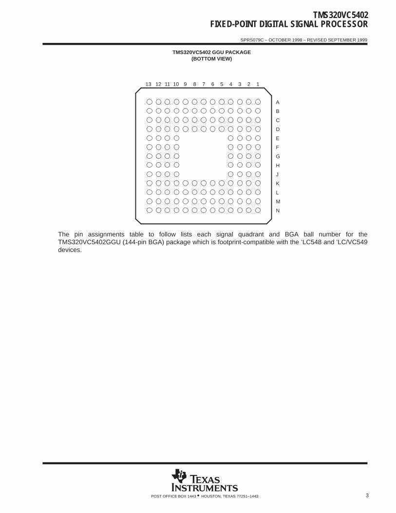
3POST OFFICE BOX 1443 • HOUSTON, TEXAS 77251–1443
TMS320VC5402 GGU PACKAGE(BOTTOM VIEW)
A
B
D
C
E
F
H
J
L
M
K
N
G
123456781012 1113 9
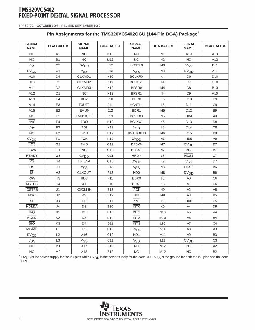
The pin assignments table to follow lists each signal quadrant and BGA ball number for theTMS320VC5402GGU (144-pin BGA) package which is footprint-compatible with the ’LC548 and ’LC/VC549devices.
TMS320VC5402FIXED-POINT DIGITAL SIGNAL PROCESSOR
SPRS079C – OCTOBER 1998 – REVISED SEPTEMBER 1999
4 POST OFFICE BOX 1443 • HOUSTON, TEXAS 77251–1443
Pin Assignments for the TMS320VC5402GGU (144-Pin BGA) Package †
SIGNALNAME BGA BALL #
SIGNALNAME BGA BALL #
SIGNALNAME BGA BALL #
SIGNALNAME BGA BALL #
NC A1 NC N13 NC N1 A19 A13
NC B1 NC M13 NC N2 NC A12
VSS C2 DVDD L12 HCNTL0 M3 VSS B11
DVDD C1 VSS L13 VSS N3 DVDD A11
A10 D4 CLKMD1 K10 BCLKR0 K4 D6 D10
HD7 D3 CLKMD2 K11 BCLKR1 L4 D7 C10
A11 D2 CLKMD3 K12 BFSR0 M4 D8 B10
A12 D1 NC K13 BFSR1 N4 D9 A10
A13 E4 HD2 J10 BDR0 K5 D10 D9
A14 E3 TOUT0 J11 HCNTL1 L5 D11 C9
A15 E2 EMU0 J12 BDR1 M5 D12 B9
NC E1 EMU1/OFF J13 BCLKX0 N5 HD4 A9
HAS F4 TDO H10 BCLKX1 K6 D13 D8
VSS F3 TDI H11 VSS L6 D14 C8
NC F2 TRST H12 HINT/TOUT1 M6 D15 B8
CVDD F1 TCK H13 CVDD N6 HD5 A8
HCS G2 TMS G12 BFSX0 M7 CVDD B7
HR/W G1 NC G13 BFSX1 N7 NC A7
READY G3 CVDD G11 HRDY L7 HDS1 C7
PS G4 HPIENA G10 DVDD K7 VSS D7
DS H1 VSS F13 VSS N8 HDS2 A6
IS H2 CLKOUT F12 HD0 M8 DVDD B6
R/W H3 HD3 F11 BDX0 L8 A0 C6
MSTRB H4 X1 F10 BDX1 K8 A1 D6
IOSTRB J1 X2/CLKIN E13 IACK N9 A2 A5
MSC J2 RS E12 HBIL M9 A3 B5
XF J3 D0 E11 NMI L9 HD6 C5
HOLDA J4 D1 E10 INT0 K9 A4 D5
IAQ K1 D2 D13 INT1 N10 A5 A4
HOLD K2 D3 D12 INT2 M10 A6 B4
BIO K3 D4 D11 INT3 L10 A7 C4
MP/MC L1 D5 C13 CVDD N11 A8 A3
DVDD L2 A16 C12 HD1 M11 A9 B3
VSS L3 VSS C11 VSS L11 CVDD C3
NC M1 A17 B13 NC N12 NC A2
NC M2 A18 B12 NC M12 NC B2† DVDD is the power supply for the I/O pins while CVDD is the power supply for the core CPU. VSS is the ground for both the I/O pins and the core
CPU.
TMS320VC5402FIXED-POINT DIGITAL SIGNAL PROCESSOR
SPRS079C – OCTOBER 1998 – REVISED SEPTEMBER 1999
5POST OFFICE BOX 1443 • HOUSTON, TEXAS 77251–1443
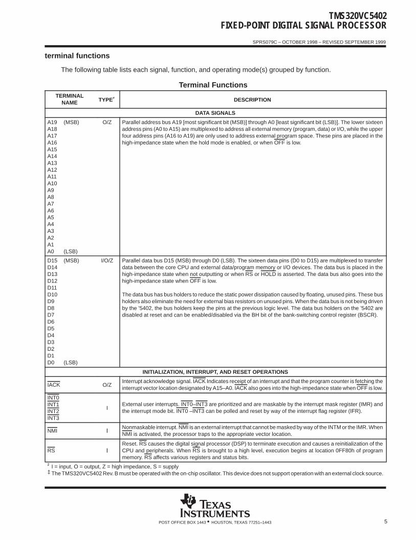
terminal functions
The following table lists each signal, function, and operating mode(s) grouped by function.
Terminal Functions TERMINAL
TYPE† DESCRIPTIONNAME TYPE† DESCRIPTION
DATA SIGNALS
A19 (MSB)A18A17A16A15A14A13A12A11A10A9A8A7A6A5A4A3A2A1A0 (LSB)
O/Z Parallel address bus A19 [most significant bit (MSB)] through A0 [least significant bit (LSB)]. The lower sixteenaddress pins (A0 to A15) are multiplexed to address all external memory (program, data) or I/O, while the upperfour address pins (A16 to A19) are only used to address external program space. These pins are placed in thehigh-impedance state when the hold mode is enabled, or when OFF is low.
D15 (MSB)D14D13D12D11D10D9D8D7D6D5D4D3D2D1D0 (LSB)
I/O/Z Parallel data bus D15 (MSB) through D0 (LSB). The sixteen data pins (D0 to D15) are multiplexed to transferdata between the core CPU and external data/program memory or I/O devices. The data bus is placed in thehigh-impedance state when not outputting or when RS or HOLD is asserted. The data bus also goes into thehigh-impedance state when OFF is low.
The data bus has bus holders to reduce the static power dissipation caused by floating, unused pins. These busholders also eliminate the need for external bias resistors on unused pins. When the data bus is not being drivenby the ’5402, the bus holders keep the pins at the previous logic level. The data bus holders on the ’5402 aredisabled at reset and can be enabled/disabled via the BH bit of the bank-switching control register (BSCR).
INITIALIZATION, INTERRUPT, AND RESET OPERATIONS
IACK O/ZInterrupt acknowledge signal. IACK Indicates receipt of an interrupt and that the program counter is fetching theinterrupt vector location designated by A15–A0. IACK also goes into the high-impedance state when OFF is low.
INT0INT1INT2INT3
IExternal user interrupts. INT0–INT3 are prioritized and are maskable by the interrupt mask register (IMR) andthe interrupt mode bit. INT0 –INT3 can be polled and reset by way of the interrupt flag register (IFR).
NMI INonmaskable interrupt. NMI is an external interrupt that cannot be masked by way of the INTM or the IMR. WhenNMI is activated, the processor traps to the appropriate vector location.
RS IReset. RS causes the digital signal processor (DSP) to terminate execution and causes a reinitialization of theCPU and peripherals. When RS is brought to a high level, execution begins at location 0FF80h of programmemory. RS affects various registers and status bits.
† I = input, O = output, Z = high impedance, S = supply‡ The TMS320VC5402 Rev. B must be operated with the on-chip oscillator. This device does not support operation with an external clock source.
TMS320VC5402FIXED-POINT DIGITAL SIGNAL PROCESSOR
SPRS079C – OCTOBER 1998 – REVISED SEPTEMBER 1999
6 POST OFFICE BOX 1443 • HOUSTON, TEXAS 77251–1443
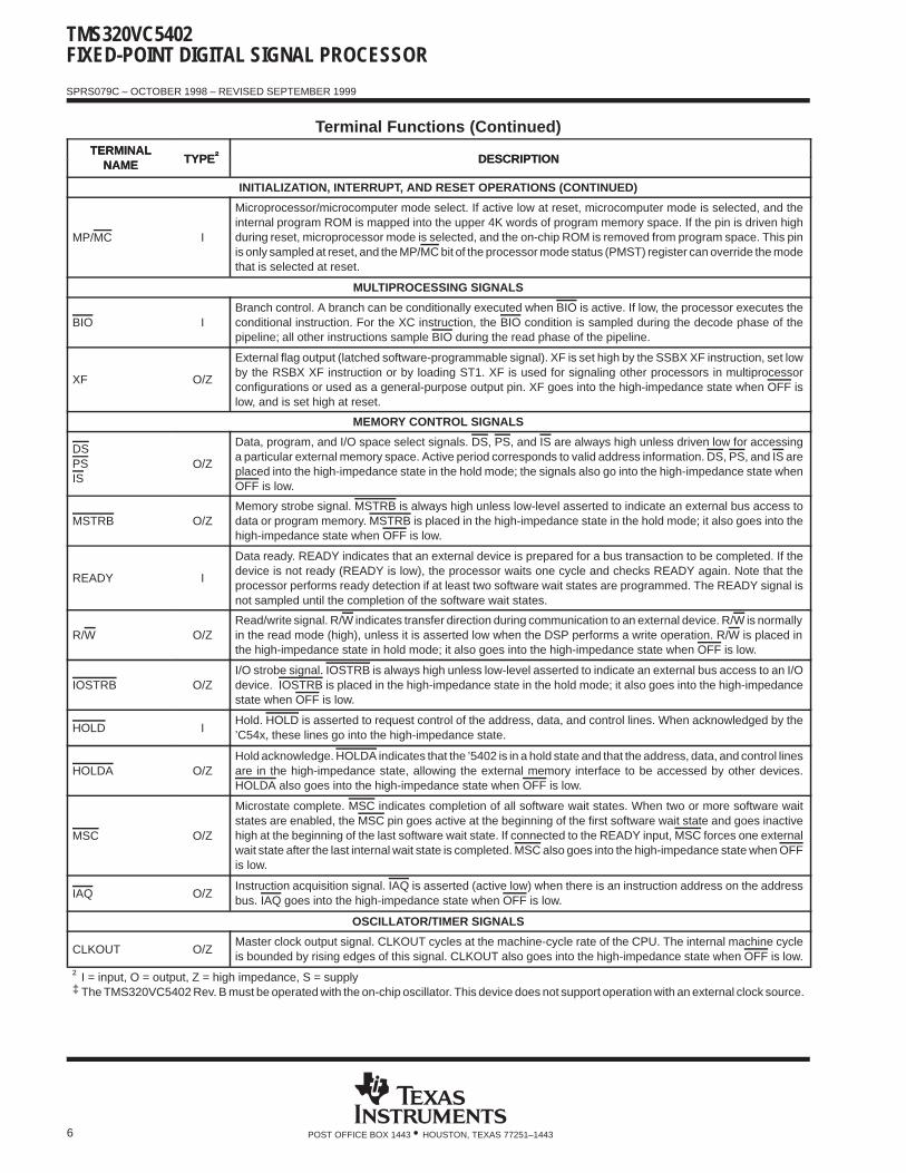
Terminal Functions (Continued)TERMINAL
NAME DESCRIPTIONTYPE†TERMINALNAME DESCRIPTIONTYPE†
INITIALIZATION, INTERRUPT, AND RESET OPERATIONS (CONTINUED)
MP/MC I
Microprocessor/microcomputer mode select. If active low at reset, microcomputer mode is selected, and theinternal program ROM is mapped into the upper 4K words of program memory space. If the pin is driven highduring reset, microprocessor mode is selected, and the on-chip ROM is removed from program space. This pinis only sampled at reset, and the MP/MC bit of the processor mode status (PMST) register can override the modethat is selected at reset.
MULTIPROCESSING SIGNALS
BIO IBranch control. A branch can be conditionally executed when BIO is active. If low, the processor executes theconditional instruction. For the XC instruction, the BIO condition is sampled during the decode phase of thepipeline; all other instructions sample BIO during the read phase of the pipeline.
XF O/Z
External flag output (latched software-programmable signal). XF is set high by the SSBX XF instruction, set lowby the RSBX XF instruction or by loading ST1. XF is used for signaling other processors in multiprocessorconfigurations or used as a general-purpose output pin. XF goes into the high-impedance state when OFF islow, and is set high at reset.
MEMORY CONTROL SIGNALS
DSPSIS
O/Z
Data, program, and I/O space select signals. DS, PS, and IS are always high unless driven low for accessinga particular external memory space. Active period corresponds to valid address information. DS, PS, and IS areplaced into the high-impedance state in the hold mode; the signals also go into the high-impedance state whenOFF is low.
MSTRB O/ZMemory strobe signal. MSTRB is always high unless low-level asserted to indicate an external bus access todata or program memory. MSTRB is placed in the high-impedance state in the hold mode; it also goes into thehigh-impedance state when OFF is low.
READY I
Data ready. READY indicates that an external device is prepared for a bus transaction to be completed. If thedevice is not ready (READY is low), the processor waits one cycle and checks READY again. Note that theprocessor performs ready detection if at least two software wait states are programmed. The READY signal isnot sampled until the completion of the software wait states.
R/W O/ZRead/write signal. R/W indicates transfer direction during communication to an external device. R/W is normallyin the read mode (high), unless it is asserted low when the DSP performs a write operation. R/W is placed inthe high-impedance state in hold mode; it also goes into the high-impedance state when OFF is low.
IOSTRB O/ZI/O strobe signal. IOSTRB is always high unless low-level asserted to indicate an external bus access to an I/Odevice. IOSTRB is placed in the high-impedance state in the hold mode; it also goes into the high-impedancestate when OFF is low.
HOLD IHold. HOLD is asserted to request control of the address, data, and control lines. When acknowledged by the’C54x, these lines go into the high-impedance state.
HOLDA O/ZHold acknowledge. HOLDA indicates that the ’5402 is in a hold state and that the address, data, and control linesare in the high-impedance state, allowing the external memory interface to be accessed by other devices.HOLDA also goes into the high-impedance state when OFF is low.
MSC O/Z
Microstate complete. MSC indicates completion of all software wait states. When two or more software waitstates are enabled, the MSC pin goes active at the beginning of the first software wait state and goes inactivehigh at the beginning of the last software wait state. If connected to the READY input, MSC forces one externalwait state after the last internal wait state is completed. MSC also goes into the high-impedance state when OFFis low.
IAQ O/ZInstruction acquisition signal. IAQ is asserted (active low) when there is an instruction address on the addressbus. IAQ goes into the high-impedance state when OFF is low.
OSCILLATOR/TIMER SIGNALS
CLKOUT O/ZMaster clock output signal. CLKOUT cycles at the machine-cycle rate of the CPU. The internal machine cycleis bounded by rising edges of this signal. CLKOUT also goes into the high-impedance state when OFF is low.
† I = input, O = output, Z = high impedance, S = supply‡ The TMS320VC5402 Rev. B must be operated with the on-chip oscillator. This device does not support operation with an external clock source.
TMS320VC5402FIXED-POINT DIGITAL SIGNAL PROCESSOR
SPRS079C – OCTOBER 1998 – REVISED SEPTEMBER 1999
7POST OFFICE BOX 1443 • HOUSTON, TEXAS 77251–1443
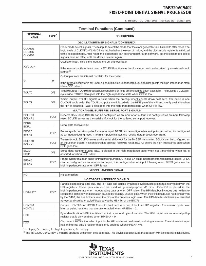
Terminal Functions (Continued)TERMINAL
NAME DESCRIPTIONTYPE†TERMINALNAME DESCRIPTIONTYPE†
OSCILLATOR/TIMER SIGNALS (CONTINUED)
CLKMD1CLKMD2CLKMD3
I
Clock mode select signals. These inputs select the mode that the clock generator is initialized to after reset. Thelogic levels of CLKMD1–CLKMD3 are latched when the reset pin is low, and the clock mode register is initializedto the selected mode. After reset, the clock mode can be changed through software, but the clock mode selectsignals have no effect until the device is reset again.
X2/CLKIN I
Oscillator input. This is the input to the on-chip oscillator.
If the internal oscillator is not used, X2/CLKIN functions as the clock input, and can be driven by an external clocksource.‡
X1 O
Output pin from the internal oscillator for the crystal.
If the internal oscillator is not used, X1 should be left unconnected. X1 does not go into the high-impedance statewhen OFF is low.‡
TOUT0 O/ZTimer0 output. TOUT0 signals a pulse when the on-chip timer 0 counts down past zero. The pulse is a CLKOUTcycle wide. TOUT0 also goes into the high-impedance state when OFF is low.
TOUT1 O/ZTimer1 output. TOUT1 signals a pulse when the on-chip timer1 counts down past zero. The pulse is oneCLKOUT cycle wide. The TOUT1 output is multiplexed with the HINT pin of the HPI and is only available whenthe HPI is disabled. TOUT1 also goes into the high-impedance state when OFF is low.
MULTICHANNEL BUFFERED SERIAL PORT SIGNALS
BCLKR0BCLKR1
I/O/ZReceive clock input. BCLKR can be configured as an input or an output; it is configured as an input followingreset. BCLKR serves as the serial shift clock for the buffered serial port receiver.
BDR0BDR1
I Serial data receive input
BFSR0BFSR1
I/O/ZFrame synchronization pulse for receive input. BFSR can be configured as an input or an output; it is configuredas an input following reset. The BFSR pulse initiates the receive data process over BDR.
BCLKX0BCLKX1
I/O/ZTransmit clock. BCLKX serves as the serial shift clock for the McBSP transmitter. BCLKX can be configured asan input or an output; it is configured as an input following reset. BCLKX enters the high-impedance state whenOFF goes low.
BDX0BDX1
O/ZSerial data transmit output. BDX is placed in the high-impedance state when not transmitting, when RS isasserted, or when OFF is low.
BFSX0BFSX1
I/O/ZFrame synchronization pulse for transmit input/output. The BFSX pulse initiates the transmit data process. BFSXcan be configured as an input or an output; it is configured as an input following reset. BFSX goes into thehigh-impedance state when OFF is low.
MISCELLANEOUS SIGNAL
NC No connection
HOST-PORT INTERFACE SIGNALS
HD0–HD7 I/O/Z
Parallel bidirectional data bus. The HPI data bus is used by a host device bus to exchange information with theHPI registers. These pins can also be used as general-purpose I/O pins. HD0–HD7 is placed in thehigh-impedance state when not outputting data or when OFF is low. The HPI data bus includes bus holders toreduce the static power dissipation caused by floating, unused pins. When the HPI data bus is not being drivenby the ’5402, the bus holders keep the pins at the previous logic level. The HPI data bus holders are disabledat reset and can be enabled/disabled via the HBH bit of the BSCR.
HCNTL0HCNTL1
IControl. HCNTL0 and HCNTL1 select a host access to one of the three HPI registers. The control inputs haveinternal pullup resistors that are only enabled when HPIENA = 0.
HBIL IByte identification. HBIL identifies the first or second byte of transfer. The HBIL input has an internal pullupresistor that is only enabled when HPIENA = 0.
HCS IChip select. HCS is the select input for the HPI and must be driven low during accesses. The chip-select inputhas an internal pullup resistor that is only enabled when HPIENA = 0.
† I = input, O = output, Z = high impedance, S = supply‡ The TMS320VC5402 Rev. B must be operated with the on-chip oscillator. This device does not support operation with an external clock source.
TMS320VC5402FIXED-POINT DIGITAL SIGNAL PROCESSOR
SPRS079C – OCTOBER 1998 – REVISED SEPTEMBER 1999
8 POST OFFICE BOX 1443 • HOUSTON, TEXAS 77251–1443
Terminal Functions (Continued)TERMINAL
NAME DESCRIPTIONTYPE†TERMINALNAME DESCRIPTIONTYPE†
HOST-PORT INTERFACE SIGNALS (CONTINUED)
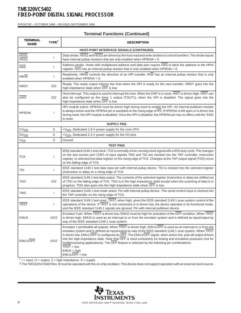
HDS1HDS2
IData strobe. HDS1 and HDS2 are driven by the host read and write strobes to control transfers. The strobe inputshave internal pullup resistors that are only enabled when HPIENA = 0.
HAS IAddress strobe. Hosts with multiplexed address and data pins require HAS to latch the address in the HPIAregister. HAS has an internal pullup resistor that is only enabled when HPIENA = 0.
HR/W IRead/write. HR/W controls the direction of an HPI transfer. R/W has an internal pullup resistor that is onlyenabled when HPIENA = 0.
HRDY O/ZReady. The ready output informs the host when the HPI is ready for the next transfer. HRDY goes into thehigh-impedance state when OFF is low.
HINT O/ZHost interrupt. This output is used to interrupt the host. When the DSP is in reset, HINT is driven high. HINT canalso be configured as the timer 1 output (TOUT1), when the HPI is disabled. The signal goes into thehigh-impedance state when OFF is low.
HPIENA I
HPI module select. HPIENA must be driven high during reset to enable the HPI. An internal pulldown resistoris always active and the HPIENA pin is sampled on the rising edge of RS. If HPIENA is left open or is driven lowduring reset, the HPI module is disabled. Once the HPI is disabled, the HPIENA pin has no effect until the ’5402is reset.
SUPPLY PNS
CVDD S +VDD. Dedicated 1.8-V power supply for the core CPU
DVDD S +VDD. Dedicated 3.3-V power supply for the I/O pins
VSS S Ground
TEST PINS
TCK I
IEEE standard 1149.1 test clock. TCK is normally a free-running clock signal with a 50% duty cycle. The changeson the test access port (TAP) of input signals TMS and TDI are clocked into the TAP controller, instructionregister, or selected test data register on the rising edge of TCK. Changes at the TAP output signal (TDO) occuron the falling edge of TCK.
TDI IIEEE standard 1149.1 test data input pin with internal pullup device. TDI is clocked into the selected register(instruction or data) on a rising edge of TCK.
TDO O/ZIEEE standard 1149.1 test data output. The contents of the selected register (instruction or data) are shifted outof TDO on the falling edge of TCK. TDO is in the high-impedance state except when the scanning of data is inprogress. TDO also goes into the high-impedance state when OFF is low.
TMS IIEEE standard 1149.1 test mode select. Pin with internal pullup device. This serial control input is clocked intothe TAP controller on the rising edge of TCK.
TRST IIEEE standard 1149.1 test reset. TRST, when high, gives the IEEE standard 1149.1 scan system control of theoperations of the device. If TRST is not connected or is driven low, the device operates in its functional mode,and the IEEE standard 1149.1 signals are ignored. Pin with internal pulldown device.
EMU0 I/O/ZEmulator 0 pin. When TRST is driven low, EMU0 must be high for activation of the OFF condition. When TRSTis driven high, EMU0 is used as an interrupt to or from the emulator system and is defined as input/output byway of the IEEE standard 1149.1 scan system.
EMU1/OFF I/O/Z
Emulator 1 pin/disable all outputs. When TRST is driven high, EMU1/OFF is used as an interrupt to or from theemulator system and is defined as input/output by way of the IEEE standard 1149.1 scan system. When TRSTis driven low, EMU1/OFF is configured as OFF. The EMU1/OFF signal, when active low, puts all output driversinto the high-impedance state. Note that OFF is used exclusively for testing and emulation purposes (not formultiprocessing applications). The OFF feature is selected by the following pin combinations:TRST = lowEMU0 = highEMU1/OFF = low
† I = input, O = output, Z = high impedance, S = supply‡ The TMS320VC5402 Rev. B must be operated with the on-chip oscillator. This device does not support operation with an external clock source.
TMS320VC5402FIXED-POINT DIGITAL SIGNAL PROCESSOR
SPRS079C – OCTOBER 1998 – REVISED SEPTEMBER 1999
9POST OFFICE BOX 1443 • HOUSTON, TEXAS 77251–1443
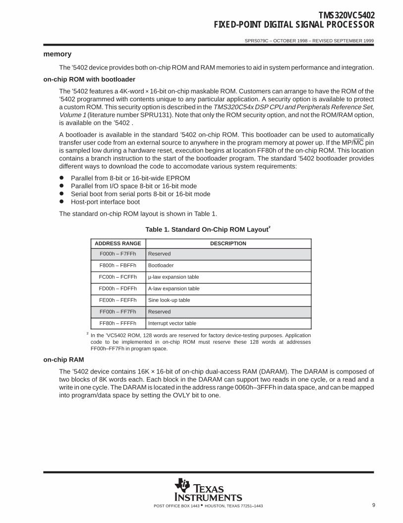
memory
The ’5402 device provides both on-chip ROM and RAM memories to aid in system performance and integration.
on-chip ROM with bootloader
The ’5402 features a 4K-word × 16-bit on-chip maskable ROM. Customers can arrange to have the ROM of the’5402 programmed with contents unique to any particular application. A security option is available to protecta custom ROM. This security option is described in the TMS320C54x DSP CPU and Peripherals Reference Set,Volume 1 (literature number SPRU131). Note that only the ROM security option, and not the ROM/RAM option,is available on the ’5402 .
A bootloader is available in the standard ’5402 on-chip ROM. This bootloader can be used to automaticallytransfer user code from an external source to anywhere in the program memory at power up. If the MP/MC pinis sampled low during a hardware reset, execution begins at location FF80h of the on-chip ROM. This locationcontains a branch instruction to the start of the bootloader program. The standard ’5402 bootloader providesdifferent ways to download the code to accomodate various system requirements:
Parallel from 8-bit or 16-bit-wide EPROM Parallel from I/O space 8-bit or 16-bit mode Serial boot from serial ports 8-bit or 16-bit mode Host-port interface boot
The standard on-chip ROM layout is shown in Table 1.
Table 1. Standard On-Chip ROM Layout †
ADDRESS RANGE DESCRIPTION
F000h – F7FFh Reserved
F800h – FBFFh Bootloader
FC00h – FCFFh µ-law expansion table
FD00h – FDFFh A-law expansion table
FE00h – FEFFh Sine look-up table
FF00h – FF7Fh Reserved
FF80h – FFFFh Interrupt vector table
† In the ’VC5402 ROM, 128 words are reserved for factory device-testing purposes. Applicationcode to be implemented in on-chip ROM must reserve these 128 words at addressesFF00h–FF7Fh in program space.
on-chip RAM
The ’5402 device contains 16K × 16-bit of on-chip dual-access RAM (DARAM). The DARAM is composed oftwo blocks of 8K words each. Each block in the DARAM can support two reads in one cycle, or a read and awrite in one cycle. The DARAM is located in the address range 0060h–3FFFh in data space, and can be mappedinto program/data space by setting the OVLY bit to one.
TMS320VC5402FIXED-POINT DIGITAL SIGNAL PROCESSOR
SPRS079C – OCTOBER 1998 – REVISED SEPTEMBER 1999
10 POST OFFICE BOX 1443 • HOUSTON, TEXAS 77251–1443
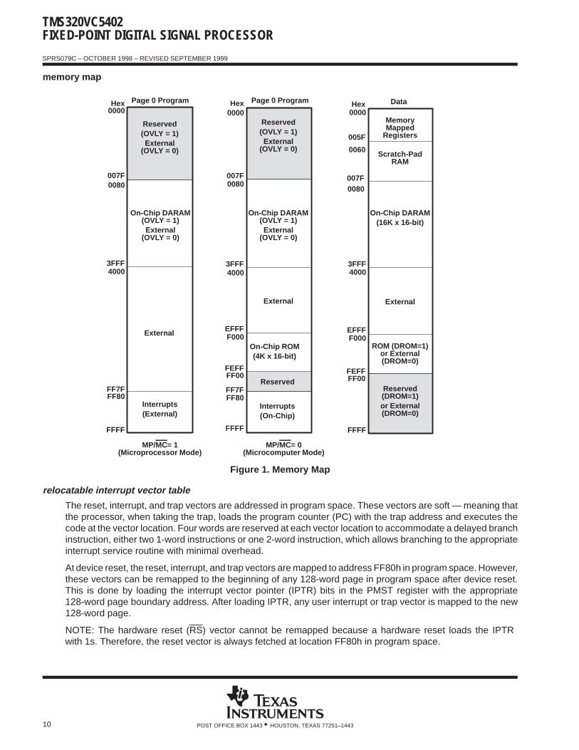
memory map
Page 0 ProgramHex Data
On-Chip DARAM(OVLY = 1)External
(OVLY = 0)
MP/MC= 0(Microcomputer Mode)
MP/MC= 1(Microprocessor Mode)
0000
007F0080
FFFF
Reserved(OVLY = 1)External
(OVLY = 0)
Interrupts(External)
FF80
MemoryMapped
Registers
On-Chip DARAM(16K x 16-bit)
ROM (DROM=1)or External(DROM=0)
0080
FFFF
Hex0000
FF7FFF00FEFF
EFFFF000
FFFF
3FFF4000
0060
007F
0000HexPage 0 Program
External
External
Scratch-PadRAM
Reserved(DROM=1)or External(DROM=0)
005F
Reserved(OVLY = 1)External
(OVLY = 0)
007F0080
3FFF4000
On-Chip DARAM(OVLY = 1)External
(OVLY = 0)
FF00FEFF
EFFFF000
External
On-Chip ROM(4K x 16-bit)
Interrupts(On-Chip)
3FFF4000
ReservedFF7FFF80
Figure 1. Memory Map
relocatable interrupt vector table
The reset, interrupt, and trap vectors are addressed in program space. These vectors are soft — meaning thatthe processor, when taking the trap, loads the program counter (PC) with the trap address and executes thecode at the vector location. Four words are reserved at each vector location to accommodate a delayed branchinstruction, either two 1-word instructions or one 2-word instruction, which allows branching to the appropriateinterrupt service routine with minimal overhead.
At device reset, the reset, interrupt, and trap vectors are mapped to address FF80h in program space. However,these vectors can be remapped to the beginning of any 128-word page in program space after device reset.This is done by loading the interrupt vector pointer (IPTR) bits in the PMST register with the appropriate128-word page boundary address. After loading IPTR, any user interrupt or trap vector is mapped to the new128-word page.
NOTE: The hardware reset (RS) vector cannot be remapped because a hardware reset loads the IPTR with 1s. Therefore, the reset vector is always fetched at location FF80h in program space.
TMS320VC5402FIXED-POINT DIGITAL SIGNAL PROCESSOR
SPRS079C – OCTOBER 1998 – REVISED SEPTEMBER 1999
11POST OFFICE BOX 1443 • HOUSTON, TEXAS 77251–1443
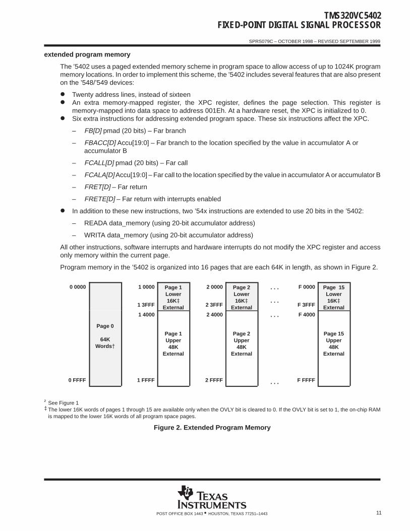
extended program memory
The ’5402 uses a paged extended memory scheme in program space to allow access of up to 1024K programmemory locations. In order to implement this scheme, the ’5402 includes several features that are also presenton the ’548/’549 devices:
Twenty address lines, instead of sixteen An extra memory-mapped register, the XPC register, defines the page selection. This register is
memory-mapped into data space to address 001Eh. At a hardware reset, the XPC is initialized to 0. Six extra instructions for addressing extended program space. These six instructions affect the XPC.
– FB[D] pmad (20 bits) – Far branch
– FBACC[D] Accu[19:0] – Far branch to the location specified by the value in accumulator A or accumulator B
– FCALL[D] pmad (20 bits) – Far call
– FCALA[D] Accu[19:0] – Far call to the location specified by the value in accumulator A or accumulator B
– FRET[D] – Far return
– FRETE[D] – Far return with interrupts enabled
In addition to these new instructions, two ’54x instructions are extended to use 20 bits in the ’5402:
– READA data_memory (using 20-bit accumulator address)
– WRITA data_memory (using 20-bit accumulator address)
All other instructions, software interrupts and hardware interrupts do not modify the XPC register and accessonly memory within the current page.
Program memory in the ’5402 is organized into 16 pages that are each 64K in length, as shown in Figure 2.
0 0000 1 0000
1 3FFF
Page 1Lower16K
External
2 0000
2 3FFF
Page 2Lower16K
External
. . .
. . .
F 0000
F 3FFF
Page 15Lower16K
External
0 FFFF
Page 0
64KWords
1 4000
1 FFFF
Page 1Upper48K
External
2 4000
2 FFFF
Page 2Upper48K
External
. . .
. . .
F 4000
F FFFF
Page 15Upper48K
External
† See Figure 1‡ The lower 16K words of pages 1 through 15 are available only when the OVLY bit is cleared to 0. If the OVLY bit is set to 1, the on-chip RAM
is mapped to the lower 16K words of all program space pages.
Figure 2. Extended Program Memory
TMS320VC5402FIXED-POINT DIGITAL SIGNAL PROCESSOR
SPRS079C – OCTOBER 1998 – REVISED SEPTEMBER 1999
12 POST OFFICE BOX 1443 • HOUSTON, TEXAS 77251–1443
on-chip peripherals
The ’5402 device has the following peripherals:
Software-programmable wait-state generator with programmable bank-switching wait states An enhanced 8-bit host-port interface (HPI8) Two multichannel buffered serial ports (McBSPs) Two hardware timers A clock generator with a phase-locked loop (PLL) A direct memory access (DMA) controller
software-programmable wait-state generator
The software wait-state generator of the ’5402 can extend external bus cycles by up to fourteen machine cycles.Devices that require more than fourteen wait states can be interfaced using the hardware READY line. Whenall external accesses are configured for zero wait states, the internal clocks to the wait-state generator areautomatically disabled. Disabling the wait-state generator clocks reduces the power comsumption of the ’5402.
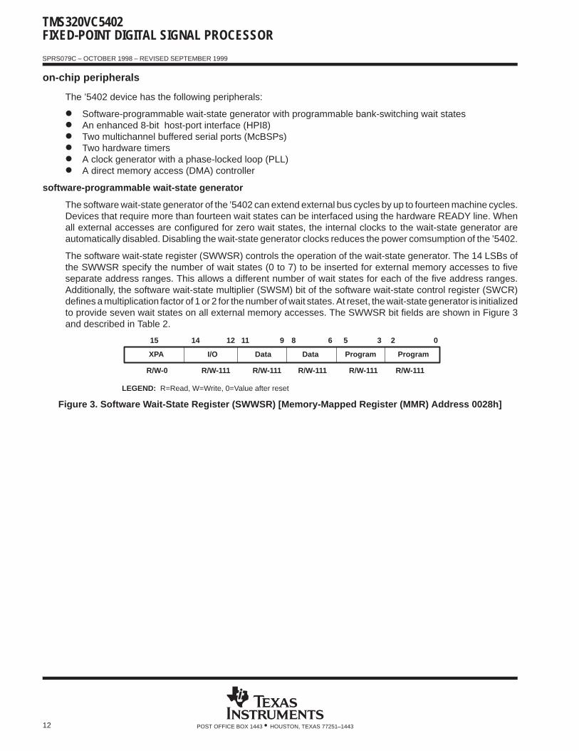
The software wait-state register (SWWSR) controls the operation of the wait-state generator. The 14 LSBs ofthe SWWSR specify the number of wait states (0 to 7) to be inserted for external memory accesses to fiveseparate address ranges. This allows a different number of wait states for each of the five address ranges.Additionally, the software wait-state multiplier (SWSM) bit of the software wait-state control register (SWCR)defines a multiplication factor of 1 or 2 for the number of wait states. At reset, the wait-state generator is initializedto provide seven wait states on all external memory accesses. The SWWSR bit fields are shown in Figure 3and described in Table 2.
XPA I/O Data Data Program Program
14 12 11 9 8 6 5 3 2 015
R/W-111R/W-0 R/W-111 R/W-111 R/W-111 R/W-111
LEGEND: R=Read, W=Write, 0=Value after reset
Figure 3. Software Wait-State Register (SWWSR) [Memory-Mapped Register (MMR) Address 0028h]
TMS320VC5402FIXED-POINT DIGITAL SIGNAL PROCESSOR
SPRS079C – OCTOBER 1998 – REVISED SEPTEMBER 1999
13POST OFFICE BOX 1443 • HOUSTON, TEXAS 77251–1443
software-programmable wait-state generator (continued)
Table 2. Software Wait-State Register (SWWSR) Bit Fields
BIT RESETFUNCTION
NO. NAME VALUEFUNCTION
15 XPA 0Extended program address control bit. XPA is used in conjunction with the program space fields(bits 0 through 5) to select the address range for program space wait states.
14–12 I/O 1I/O space. The field value (0–7) corresponds to the base number of wait states for I/O space accesseswithin addresses 0000–FFFFh. The SWSM bit of the SWCR defines a multiplication factor of 1 or 2 forthe base number of wait states.
11–9 Data 1Upper data space. The field value (0–7) corresponds to the base number of wait states for externaldata space accesses within addresses 8000–FFFFh. The SWSM bit of the SWCR defines amultiplication factor of 1 or 2 for the base number of wait states.
8–6 Data 1Lower data space. The field value (0–7) corresponds to the base number of wait states for externaldata space accesses within addresses 0000–7FFFh. The SWSM bit of the SWCR defines amultiplication factor of 1 or 2 for the base number of wait states.
5–3 Program 1
Upper program space. The field value (0–7) corresponds to the base number of wait states for externalprogram space accesses within the following addresses:
XPA = 0: x8000 – xFFFFh
XPA = 1: The upper program space bit field has no effect on wait states.
The SWSM bit of the SWCR defines a multiplication factor of 1 or 2 for the base number of waitstates.
2–0 Program 1
Program space. The field value (0–7) corresponds to the base number of wait states for externalprogram space accesses within the following addresses:
XPA = 0: x0000–x7FFFh
XPA = 1: 00000–FFFFFh
The SWSM bit of the SWCR defines a multiplication factor of 1 or 2 for the base number of waitstates.
The software wait-state multiplier bit of the software wait-state control register (SWCR) is used to extend thebase number of wait states selected by the SWWSR. The SWCR bit fields are shown in Figure 4 and describedin Table 3.
Reserved
115
R/W-0
SWSM
0
R/W-0
LEGEND: R = Read, W = Write
Figure 4. Software Wait-State Control Register (SWCR) [MMR Address 002Bh]
Table 3. Software Wait-State Control Register (SWCR) Bit Fields
PIN RESETFUNCTION
NO. NAME VALUEFUNCTION
15–1 Reserved 0 These bits are reserved and are unaffected by writes.
0 SWSM 0
Software wait-state multiplier. Used to multiply the number of wait states defined in the SWWSR by a factorof 1 or 2.
SWSM = 0: wait-state base values are unchanged (multiplied by 1).
SWSM = 1: wait-state base values are mulitplied by 2 for a maximum of 14 wait states.
TMS320VC5402FIXED-POINT DIGITAL SIGNAL PROCESSOR
SPRS079C – OCTOBER 1998 – REVISED SEPTEMBER 1999
14 POST OFFICE BOX 1443 • HOUSTON, TEXAS 77251–1443
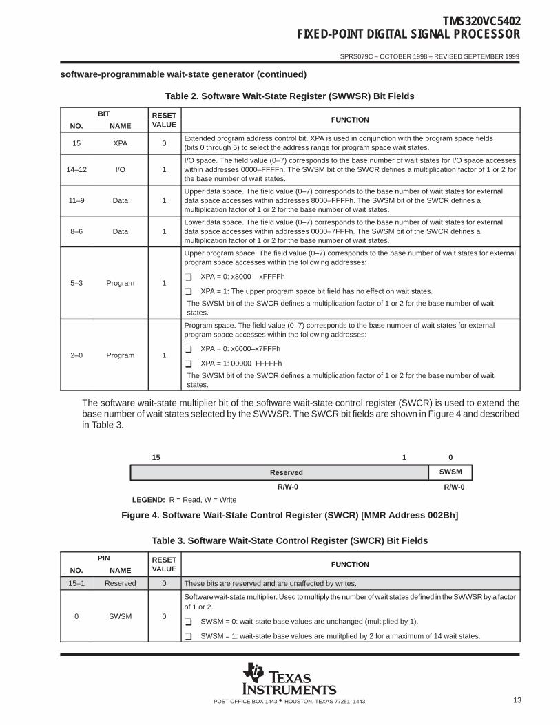
programmable bank-switching wait states
The programmable bank-switching logic of the ’5402 is functionally equivalent to that of the ’548/’549 devices.This feature automatically inserts one cycle when accesses cross memory-bank boundaries within program ordata memory space. A bank-switching wait state can also be automatically inserted when accesses cross thedata space boundary into program space.
The bank-switching control register (BSCR) defines the bank size for bank-switching wait states. Figure 5shows the BSCR and its bits are described in Table 4.
BNKCMP PS-DS Reserved HBH
12 11 3 2 115
R/W-0R-0R/W-1R/W-1111
BH EXIO
010
R/W-0R/W-0
LEGEND: R = Read, W = Write
Figure 5. Bank-Switching Control Register (BSCR), MMR Address 0029h
Table 4. Bank-Switching Control Register (BSCR) Fields
BIT RESETFUNCTION
NO. NAME VALUE FUNCTION
15–12 BNKCMP 1111Bank compare. Determines the external memory-bank size. BNKCMP is used to mask the four MSBs ofan address. For example, if BNKCMP = 1111b, the four MSBs (bits 12–15) are compared, resulting in abank size of 4K words. Bank sizes of 4K words to 64K words are allowed.
11 PS - DS 1
Program read – data read access. Inserts an extra cycle between consecutive accesses of program readand data read or data read and program read.PS-DS = 0 No extra cycles are inserted by this feature.PS-DS = 1 One extra cycle is inserted between consecutive data and program reads.
10–3 Reserved 0 These bits are reserved and are unaffected by writes.
2 HBH 0
HPI Bus holder. Controls the HPI bus holder feature. HBH is cleared to 0 at reset.HBH = 0 The bus holder is disabled.HBH = 1 The bus holder is enabled. When not driven, the HPI data bus (HD[7:0]) is held in the
previous logic level.
1 BH 0
Bus holder. Controls the data bus holder feature. BH is cleared to 0 at reset.BH = 0 The bus holder is disabled.BH = 1 The bus holder is enabled. When not driven, the data bus (D[15:0]) is held in the
previous logic level.
External bus interface off. The EXIO bit controls the external bus-off function.EXIO = 0 The external bus interface functions as usual
0 EXIO 0EXIO = 0 The external bus interface functions as usual.EXIO = 1 The address bus, data bus, and control signals become inactive after completing the
current bus cycle Note that the DROM MP/MC and OVLY bits in the PMST and the HMcurrent bus cycle. Note that the DROM, MP/MC, and OVLY bits in the PMST and the HMbit of ST1 cannot be modified when the interface is disabled.
TMS320VC5402FIXED-POINT DIGITAL SIGNAL PROCESSOR
SPRS079C – OCTOBER 1998 – REVISED SEPTEMBER 1999
15POST OFFICE BOX 1443 • HOUSTON, TEXAS 77251–1443
parallel I/O ports
The ’5402 has a total of 64K I/O ports. These ports can be addressed by the PORTR instruction or the PORTWinstruction. The IS signal indicates a read/write operation through an I/O port. The ’5402 can interface easilywith external devices through the I/O ports while requiring minimal off-chip address-decoding circuits.
enhanced 8-bit host-port interface
The ’5402 host-port interface, also referred to as the HPI8, is an enhanced version of the standard 8-bit HPIfound on earlier ’54x DSPs (’542, ’545, ’548, and ’549). The HPI8 is an 8-bit parallel port for interprocessorcommunication. The features of the HPI8 include:
Standard features:
Sequential transfers (with autoincrement) or random-access transfers Host interrupt and ’54x interrupt capability Multiple data strobes and control pins for interface flexibility
Enhanced features of the ’5402 HPI8:
Access to entire on-chip RAM through DMA bus Capability to continue transferring during emulation stop
The HPI8 functions as a slave and enables the host processor to access the on-chip memory of the ’5402. Amajor enhancement to the ’5402 HPI over previous versions is that it allows host access to the entire on-chipmemory range of the DSP. The HPI8 memory map is identical to that of the DMA controller shown in Figure 6.The host and the DSP both have access to the on-chip RAM at all times and host accesses are alwayssynchronized to the DSP clock. If the host and the DSP contend for access to the same location, the host haspriority, and the DSP waits for one HPI8 cycle. Note that since host accesses are always synchronized to the’5402 clock, an active input clock (CLKIN) is required for HPI8 accesses during IDLE states, and host accessesare not allowed while the ’5402 reset pin is asserted.
The HPI8 interface consists of an 8-bit bidirectional data bus and various control signals. Sixteen-bit transfersare accomplished in two parts with the HBIL input designating high or low byte. The host communicates withthe HPI8 through three dedicated registers — HPI address register (HPIA), HPI data register (HPID), and anHPI control register (HPIC). The HPIA and HPID registers are only accessible by the host, and the HPIC registeris accessible by both the host and the ’5402.
TMS320VC5402FIXED-POINT DIGITAL SIGNAL PROCESSOR
SPRS079C – OCTOBER 1998 – REVISED SEPTEMBER 1999
16 POST OFFICE BOX 1443 • HOUSTON, TEXAS 77251–1443
multichannel buffered serial ports
The ’5402 device includes two high-speed, full-duplex multichannel buffered serial ports (McBSPs) that allowdirect interface to other ’C54x/’LC54x devices, codecs, and other devices in a system. The McBSPs are basedon the standard serial port interface found on other ’54x devices. Like its predecessors, the McBSP provides:
Full-duplex communication Double-buffered data registers, which allow a continuous data stream Independent framing and clocking for receive and transmit
In addition, the McBSP has the following capabilities:
Direct interface to:
– T1/E1 framers
– MVIP switching compatible and ST-BUS compliant devices
– IOM-2 compliant devices
– Serial peripheral interface devices
Multichannel transmit and receive of up to 128 channels A wide selection of data sizes including 8, 12, 16, 20, 24, or 32 bits µ-law and A-law companding Programmable polarity for both frame synchronization and data clocks Programmable internal clock and frame generation
The McBSPs consist of separate transmit and receive channels that operate independently. The externalinterface of each McBSP consists of the following pins:
BCLKX Transmit reference clock BDX Transmit data BFSX Transmit frame synchronization BCLKR Receive reference clock BDR Receive data BFSR Receive frame synchronization
The six pins listed are functionally equivalent to previous serial port interface pins in the ’C5000 family of DSPs.On the transmitter, transmit frame synchronization and clocking are indicated by the BFSX and BCLKX pins,respectively. The CPU or DMA can initiate transmission of data by writing to the data transmit register (DXR).Data written to DXR is shifted out on the BDX pin through a transmit shift register (XSR). This structure allowsDXR to be loaded with the next word to be sent while the transmission of the current word is in progress.
TMS320VC5402FIXED-POINT DIGITAL SIGNAL PROCESSOR
SPRS079C – OCTOBER 1998 – REVISED SEPTEMBER 1999
17POST OFFICE BOX 1443 • HOUSTON, TEXAS 77251–1443
multichannel buffered serial ports (continued)
On the receiver, receive frame synchronization and clocking are indicated by the BFSR and BCLKR pins,respectively. The CPU or DMA can read received data from the data receive register (DRR). Data received onthe BDR pin is shifted into a receive shift register (RSR) and then buffered in the receive buffer register (RBR).If the DRR is empty, the RBR contents are copied into the DRR. If not, the RBR holds the data until the DRRis available. This structure allows storage of the two previous words while the reception of the current word isin progress.
The CPU and DMA can move data to and from the McBSPs and can synchronize transfers based on McBSPinterrupts, event signals, and status flags. The DMA is capable of handling data movement between theMcBSPs and memory with no intervention from the CPU.
In addition to the standard serial port functions, the McBSP provides programmable clock and framesynchronization signals. The programmable functions include:
Frame synchronization pulse width Frame period Frame synchronization delay Clock reference (internal vs. external) Clock division Clock and frame synchronization polarity
The on-chip companding hardware allows compression and expansion of data in either µ-law or A-law format.When companding is used, transmit data is encoded according to specified companding law and received datais decoded to 2s complement format.
The McBSP allows the multiple channels to be independently selected for the transmitter and receiver. Whenmultiple channels are selected, each frame represents a time-division multiplexed (TDM) data stream. In usingTDM data streams, the CPU may only need to process a few of them. Thus, to save memory and bus bandwidth,multichannel selection allows independent enabling of particular channels for transmission and reception. Upto 32 channels in a stream of up to 128 channels can be enabled.
The clock-stop mode (CLKSTP) in the McBSP provides compatibility with the serial peripheral interface (SPI)protocol. The word sizes supported by the McBSP are programmable for 8-, 12-, 16-, 20-, 24-, or 32-bitoperation. When the McBSP is configured to operate in SPI mode, both the transmitter and the receiver operatetogether as a master or as a slave.
The McBSP is fully static and operates at arbitrarily low clock frequencies. The maximum frequency is CPUclock frequency divided by 2.
hardware timer
The ’5402 device features two 16-bit timing circuits with 4-bit prescalers. The main counter of each timer isdecremented by one every CLKOUT cycle. Each time the counter decrements to 0, a timer interrupt isgenerated. The timers can be stopped, restarted, reset, or disabled by specific control bits.
clock generator
The clock generator provides clocks to the ’5402 device, and consists of an internal oscillator and aphase-locked loop (PLL) circuit. The clock generator requires a reference clock input, which can be providedby using a crystal resonator with the internal oscillator, or from an external clock source.
NOTE: The TMS320VC5402 Rev. B must be operated with the on-chip oscillator. This device does not supportoperation with an external clock source.
TMS320VC5402FIXED-POINT DIGITAL SIGNAL PROCESSOR
SPRS079C – OCTOBER 1998 – REVISED SEPTEMBER 1999
18 POST OFFICE BOX 1443 • HOUSTON, TEXAS 77251–1443
clock generator (continued)
The reference clock input is then divided by two (DIV mode) to generate clocks for the ’5402 device, or the PLLcircuit can be used (PLL mode) to generate the device clock by multiplying the reference clock frequency bya scale factor, allowing use of a clock source with a lower frequency than that of the CPU.The PLL is an adaptivecircuit that, once synchronized, locks onto and tracks an input clock signal.
When the PLL is initially started, it enters a transitional mode during which the PLL acquires lock with the inputsignal. Once the PLL is locked, it continues to track and maintain synchronization with the input signal. Then,other internal clock circuitry allows the synthesis of new clock frequencies for use as master clock for the ’5402device.
This clock generator allows system designers to select the clock source. The sources that drive the clockgenerator are:
A crystal resonator circuit. The crystal resonator circuit is connected across the X1 and X2/CLKIN pins ofthe ’5402 to enable the internal oscillator.
An external clock. The external clock source is directly connected to the X2/CLKIN pin, and X1 is leftunconnected.
NOTE: The TMS320VC5402 Rev. B must be operated with the on-chip oscillator. This device does not supportoperation with an external clock source.
The software-programmable PLL features a high level of flexibility, and includes a clock scaler that providesvarious clock multiplier ratios, capability to directly enable and disable the PLL, and a PLL lock timer that canbe used to delay switching to PLL clocking mode of the device until lock is achieved.Devices that have a built-insoftware-programmable PLL can be configured in one of two clock modes:
PLL mode. The input clock (X2/CLKIN) is multiplied by 1 of 31 possible ratios. These ratios are achievedusing the PLL circuitry.
DIV (divider) mode. The input clock is divided by 2 or 4. Note that when DIV mode is used, the PLL can becompletely disabled in order to minimize power dissipation.
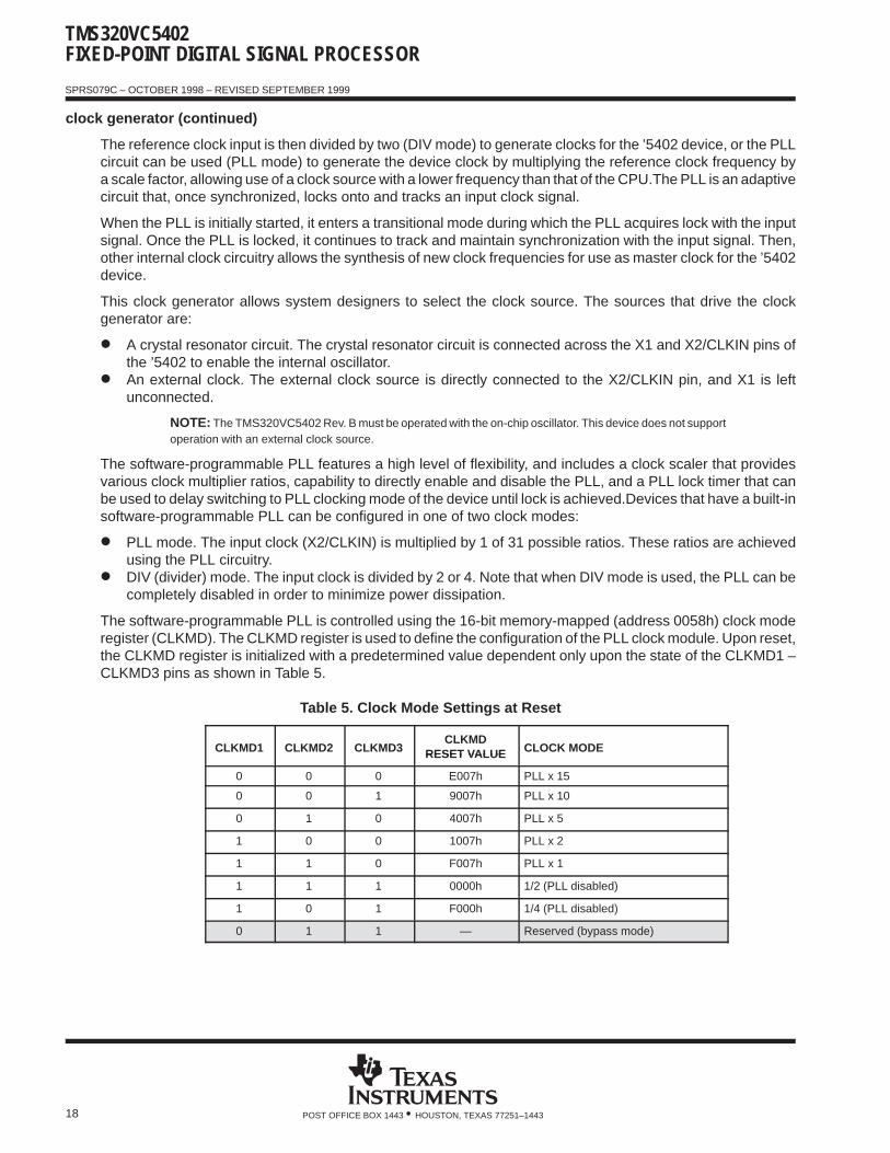
The software-programmable PLL is controlled using the 16-bit memory-mapped (address 0058h) clock moderegister (CLKMD). The CLKMD register is used to define the configuration of the PLL clock module. Upon reset,the CLKMD register is initialized with a predetermined value dependent only upon the state of the CLKMD1 –CLKMD3 pins as shown in Table 5.
Table 5. Clock Mode Settings at Reset
CLKMD1 CLKMD2 CLKMD3CLKMD
RESET VALUE CLOCK MODERESET VALUE
0 0 0 E007h PLL x 15
0 0 1 9007h PLL x 10
0 1 0 4007h PLL x 5
1 0 0 1007h PLL x 2
1 1 0 F007h PLL x 1
1 1 1 0000h 1/2 (PLL disabled)
1 0 1 F000h 1/4 (PLL disabled)
0 1 1 — Reserved (bypass mode)
TMS320VC5402FIXED-POINT DIGITAL SIGNAL PROCESSOR
SPRS079C – OCTOBER 1998 – REVISED SEPTEMBER 1999
19POST OFFICE BOX 1443 • HOUSTON, TEXAS 77251–1443
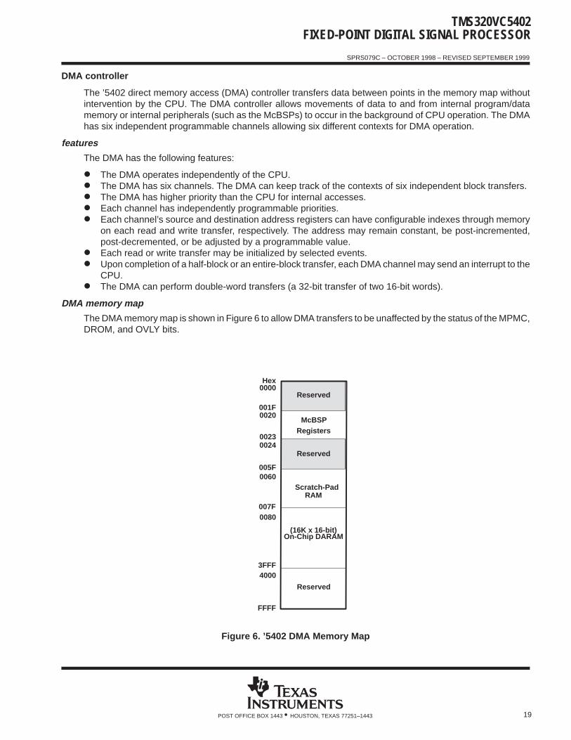
DMA controller
The ’5402 direct memory access (DMA) controller transfers data between points in the memory map withoutintervention by the CPU. The DMA controller allows movements of data to and from internal program/datamemory or internal peripherals (such as the McBSPs) to occur in the background of CPU operation. The DMAhas six independent programmable channels allowing six different contexts for DMA operation.
features
The DMA has the following features:
The DMA operates independently of the CPU. The DMA has six channels. The DMA can keep track of the contexts of six independent block transfers. The DMA has higher priority than the CPU for internal accesses. Each channel has independently programmable priorities. Each channel’s source and destination address registers can have configurable indexes through memory
on each read and write transfer, respectively. The address may remain constant, be post-incremented,post-decremented, or be adjusted by a programmable value.
Each read or write transfer may be initialized by selected events. Upon completion of a half-block or an entire-block transfer, each DMA channel may send an interrupt to the
CPU. The DMA can perform double-word transfers (a 32-bit transfer of two 16-bit words).
DMA memory map
The DMA memory map is shown in Figure 6 to allow DMA transfers to be unaffected by the status of the MPMC,DROM, and OVLY bits.
FFFF
Reserved
40003FFF
Hex0000
005F0060
On-Chip DARAM
Scratch-Pad
0080007F
(16K x 16-bit)
RAM
Reserved
McBSPRegisters
001F0020
00230024
Reserved
Figure 6. ’5402 DMA Memory Map
TMS320VC5402FIXED-POINT DIGITAL SIGNAL PROCESSOR
SPRS079C – OCTOBER 1998 – REVISED SEPTEMBER 1999
20 POST OFFICE BOX 1443 • HOUSTON, TEXAS 77251–1443
DMA priority level
Each DMA channel can be independently assigned high priority or low priority relative to each other. MultipleDMA channels that are assigned to the same priority level are handled in a round-robin manner.
DMA source/destination address modification
The DMA provides flexible address-indexing modes for easy implementation of data management schemessuch as autobuffering and circular buffers. Source and destination addresses can be indexed separately andcan be post-incremented, post-decremented, or post-incremented with a specified index offset.
DMA in autoinitialization mode
The DMA can automatically reinitialize itself after completion of a block transfer. Some of the DMA registers canbe preloaded for the next block transfer through the DMA global reload registers (DMGSA, DMGDA, andDMGCR). Autoinitialization allows:
Continuous operation: Normally, the CPU would have to reinitialize the DMA immediately after thecompletion of the current block transfer; but with the global reload registers, it can reinitialize these valuesfor the next block transfer any time after the current block transfer begins.
Repetitive operation: The CPU does not preload the global reload register with new values for each blocktransfer but only loads them on the first block transfer.
DMA transfer counting
The DMA channel element count register (DMCTRx) and the frame count register (DMSFCx) contain bit fieldsthat represent the number of frames and the number of elements per frame to be transferred.
Frame count. This 8-bit value defines the total number of frames in the block transfer. The maximum numberof frames per block transfer is 128 (FRAME COUNT= 0ffh). The counter is decremented upon the last readtransfer in a frame transfer. Once the last frame is transferred, the selected 8-bit counter is reloaded withthe DMA global frame reload register (DMGFR) if the AUTOINIT bit is set to 1. A frame count of 0 (defaultvalue) means the block transfer contains a single frame.
Element count. This 16-bit value defines the number of elements per frame. This counter is decrementedafter the read transfer of each element. The maximum number of elements per frame is 65536(DMCTRn = 0FFFFh). In autoinitialization mode, once the last frame is transferred, the counter is reloadedwith the DMA global count reload register (DMGCR).
DMA transfers in double-word mode
Double-word mode allows the DMA to transfer 32-bit words in any index mode. In double-word mode, twoconsecutive 16-bit transfers are initiated and the source and destination addresses are automatically updatedfollowing each transfer. In this mode, each 32-bit word is considered to be one element.
DMA channel index registers
The particular DMA channel index register is selected by way of the SIND and DIND field in the DMA modecontrol register (DMMCRx). Unlike basic address adjustment, in conjunction with the frame index DMFRI0 andDMFRI1, the DMA allows different adjustment amounts depending on whether or not the element transfer isthe last in the current frame. The normal adjustment value (element index) is contained in the element indexregisters DMIDX0 and DMIDX1. The adjustment value (frame index) for the end of the frame, is determined bythe selected DMA frame index register, either DMFRI0 or DMFRI1.
TMS320VC5402FIXED-POINT DIGITAL SIGNAL PROCESSOR
SPRS079C – OCTOBER 1998 – REVISED SEPTEMBER 1999
21POST OFFICE BOX 1443 • HOUSTON, TEXAS 77251–1443
DMA channel index registers (continued)
The element index and the frame index affect address adjustment as follows:
Element index: For all except the last transfer in the frame, the element index determines the amount to beadded to the DMA channel for the source/destination address register (DMSRCx/DMDSTx) as selected bythe SIND/DIND bits.
Frame index: If the transfer is the last in a frame, the frame index is used for address adjustment as selectedby the SIND/DIND bits. This occurs in both single-frame and multi-frame transfer.
DMA interrupts
The ability of the DMA to interrupt the CPU based on the status of the data transfer is configurable and isdetermined by the IMOD and DINM bits in the DMA channel mode control register (DMMCRn). The availablemodes are shown in Table 6.
Table 6. DMA Interrupts
MODE DINM IMOD INTERRUPT
ABU (non-decrement) 1 0 At full buffer only
ABU (non-decrement) 1 1 At half buffer and full buffer
Multi-Frame 1 0 At block transfer complete (DMCTRn = DMSEFCn[7:0] = 0)
Multi-Frame 1 1 At end of frame and end of block (DMCTRn = 0)
Either 0 X No interrupt generated
Either 0 X No interrupt generated
DMA controller synchronization events
The transfers associated with each DMA channel can be synchronized to one of several events. The DSYN bitfield of the DMA channel x sync select and frame count (DMSFCx) register selects the synchronization eventfor a channel. The list of possible events and the DSYN values are shown in Table 7.
Table 7. DMA Synchronization Events
DSYN VALUE DMA SYNCHRONIZATION EVENT
0000b No synchronization used
0001b McBSP0 receive event
0010b McBSP0 transmit event
0011–0100b Reserved
0101b McBSP1 receive event
0110b McBSP1 transmit event
0111b–0110b Reserved
1101b Timer0 interrupt
1110b External interrupt 3
1111b Timer1 interrupt
TMS320VC5402FIXED-POINT DIGITAL SIGNAL PROCESSOR
SPRS079C – OCTOBER 1998 – REVISED SEPTEMBER 1999
22 POST OFFICE BOX 1443 • HOUSTON, TEXAS 77251–1443
DMA channel interrupt selection
The DMA controller can generate a CPU interrupt for each of the six channels. However, channels 1, 2, and3 are multiplexed with other interrupt sources. DMA channels 2 and 3 share an interrupt line with the receiveand transmit portions of McBSP1 (IMR/IFR bits 10 and 11), and DMA channel 1 shares an interrupt line withtimer 1 (IMR/IFR bit 7). When the ’5402 is reset, the interrupts from these three DMA channels are deselected.The INTSEL bit field in the DMA channel priority and enable control (DMPREC) register can be used to selectthese interrupts, as shown in Table 8.
Table 8. DMA Channel Interrupt Selection
INTSEL Value IMR/IFR[7] IMR/IFR[10] IMR/IFR[11]
00b (reset) TINT1 BRINT1 BXINT1
01b TINT1 DMAC2 DMAC3
10b DMAC1 DMAC2 DMAC3
11b Reserved
TMS320VC5402FIXED-POINT DIGITAL SIGNAL PROCESSOR
SPRS079C – OCTOBER 1998 – REVISED SEPTEMBER 1999
23POST OFFICE BOX 1443 • HOUSTON, TEXAS 77251–1443
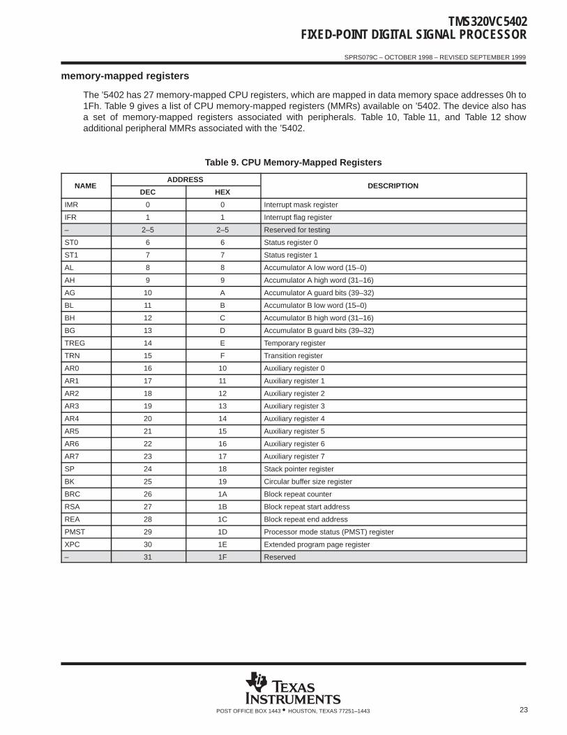
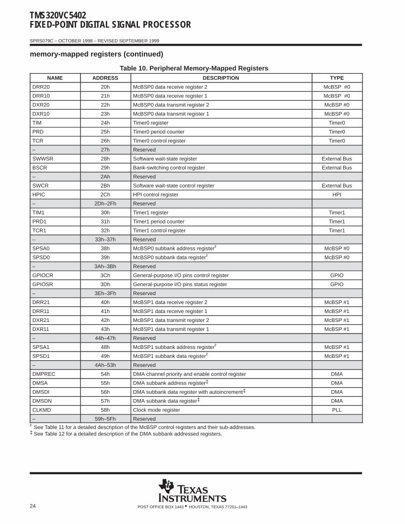
memory-mapped registers
The ’5402 has 27 memory-mapped CPU registers, which are mapped in data memory space addresses 0h to1Fh. Table 9 gives a list of CPU memory-mapped registers (MMRs) available on ’5402. The device also hasa set of memory-mapped registers associated with peripherals. Table 10, Table 11, and Table 12 showadditional peripheral MMRs associated with the ’5402.
Table 9. CPU Memory-Mapped Registers
NAMEADDRESS
DESCRIPTIONNAMEDEC HEX
DESCRIPTION
IMR 0 0 Interrupt mask register
IFR 1 1 Interrupt flag register
– 2–5 2–5 Reserved for testing
ST0 6 6 Status register 0
ST1 7 7 Status register 1
AL 8 8 Accumulator A low word (15–0)
AH 9 9 Accumulator A high word (31–16)
AG 10 A Accumulator A guard bits (39–32)
BL 11 B Accumulator B low word (15–0)
BH 12 C Accumulator B high word (31–16)
BG 13 D Accumulator B guard bits (39–32)
TREG 14 E Temporary register
TRN 15 F Transition register
AR0 16 10 Auxiliary register 0
AR1 17 11 Auxiliary register 1
AR2 18 12 Auxiliary register 2
AR3 19 13 Auxiliary register 3
AR4 20 14 Auxiliary register 4
AR5 21 15 Auxiliary register 5
AR6 22 16 Auxiliary register 6
AR7 23 17 Auxiliary register 7
SP 24 18 Stack pointer register
BK 25 19 Circular buffer size register
BRC 26 1A Block repeat counter
RSA 27 1B Block repeat start address
REA 28 1C Block repeat end address
PMST 29 1D Processor mode status (PMST) register
XPC 30 1E Extended program page register
– 31 1F Reserved
TMS320VC5402FIXED-POINT DIGITAL SIGNAL PROCESSOR
SPRS079C – OCTOBER 1998 – REVISED SEPTEMBER 1999
24 POST OFFICE BOX 1443 • HOUSTON, TEXAS 77251–1443
memory-mapped registers (continued)
Table 10. Peripheral Memory-Mapped Registers NAME ADDRESS DESCRIPTION TYPE
DRR20 20h ÁÁÁÁÁÁÁÁÁÁÁÁÁÁÁÁÁÁÁÁÁÁÁÁÁÁÁÁÁÁÁÁÁÁÁÁÁÁ
McBSP0 data receive register 2 McBSP #0
DRR10 21hÁÁÁÁÁÁÁÁÁÁÁÁÁÁÁÁÁÁÁÁÁÁÁÁÁÁÁÁÁÁÁÁÁÁÁÁÁÁMcBSP0 data receive register 1 McBSP #0
DXR20 22hÁÁÁÁÁÁÁÁÁÁÁÁÁÁÁÁÁÁÁÁÁÁÁÁÁÁÁÁÁÁÁÁÁÁÁÁÁÁMcBSP0 data transmit register 2 McBSP #0
DXR10 23hÁÁÁÁÁÁÁÁÁÁÁÁÁÁÁÁÁÁÁÁÁÁÁÁÁÁÁÁÁÁÁÁÁÁÁÁÁÁ
McBSP0 data transmit register 1 McBSP #0
TIM 24h ÁÁÁÁÁÁÁÁÁÁÁÁÁÁÁÁÁÁÁÁÁÁÁÁÁÁÁÁÁÁÁÁÁÁÁÁÁÁ
Timer0 register Timer0
PRD 25h ÁÁÁÁÁÁÁÁÁÁÁÁÁÁÁÁÁÁÁÁÁÁÁÁÁÁÁÁÁÁÁÁÁÁÁÁÁÁ
Timer0 period counter Timer0
TCR 26h ÁÁÁÁÁÁÁÁÁÁÁÁÁÁÁÁÁÁÁÁÁÁÁÁÁÁÁÁÁÁÁÁÁÁÁÁÁÁ
Timer0 control register Timer0
– 27h Reserved
SWWSR 28h ÁÁÁÁÁÁÁÁÁÁÁÁÁÁÁÁÁÁÁÁÁÁÁÁÁÁÁÁÁÁÁÁÁÁÁÁÁÁ
Software wait-state register External Bus
BSCR 29h ÁÁÁÁÁÁÁÁÁÁÁÁÁÁÁÁÁÁÁBank-switching control register External Bus
– 2Ah Reserved
SWCR 2BhÁÁÁÁÁÁÁÁÁÁÁÁÁÁÁÁÁÁÁÁÁÁÁÁÁÁÁÁÁÁÁÁÁÁÁÁÁÁ
Software wait-state control register External Bus
HPIC 2ChÁÁÁÁÁÁÁÁÁÁÁÁÁÁÁÁÁÁÁÁÁÁÁÁÁÁÁÁÁÁÁÁÁÁÁÁÁÁ
HPI control register HPI
– 2Dh–2Fh Reserved
TIM1 30h ÁÁÁÁÁÁÁÁÁÁÁÁÁÁÁÁÁÁÁÁÁÁÁÁÁÁÁÁÁÁÁÁÁÁÁÁÁÁ
Timer1 register Timer1
PRD1 31h ÁÁÁÁÁÁÁÁÁÁÁÁÁÁÁÁÁÁÁÁÁÁÁÁÁÁÁÁÁÁÁÁÁÁÁÁÁÁ
Timer1 period counter Timer1
TCR1 32h ÁÁÁÁÁÁÁÁÁÁÁÁÁÁÁÁÁÁÁÁÁÁÁÁÁÁÁÁÁÁÁÁÁÁÁÁÁÁ
Timer1 control register Timer1
– 33h–37h ReservedÁÁÁÁÁÁÁÁÁÁÁÁSPSA0
ÁÁÁÁÁÁÁÁÁÁÁÁ38h
ÁÁÁÁÁÁÁÁÁÁÁÁÁÁÁÁÁÁÁÁÁÁÁÁÁÁÁÁÁÁÁÁÁÁÁÁÁÁMcBSP0 subbank address register†
ÁÁÁÁÁÁÁÁÁÁÁÁMcBSP #0ÁÁÁÁÁÁ
ÁÁÁÁÁÁSPSD0ÁÁÁÁÁÁÁÁÁÁÁÁ39h
ÁÁÁÁÁÁÁÁÁÁÁÁÁÁÁÁÁÁÁÁÁÁÁÁÁÁÁÁÁÁÁÁÁÁÁÁÁÁMcBSP0 subbank data register†
ÁÁÁÁÁÁÁÁÁÁÁÁMcBSP #0
– 3Ah–3Bh ReservedÁÁÁÁÁÁÁÁÁÁÁÁ
GPIOCR ÁÁÁÁÁÁÁÁÁÁÁÁ
3Ch ÁÁÁÁÁÁÁÁÁÁÁÁÁÁÁÁÁÁÁÁÁÁÁÁÁÁÁÁÁÁÁÁÁÁÁÁÁÁ
General-purpose I/O pins control register ÁÁÁÁÁÁÁÁÁÁÁÁ
GPIOÁÁÁÁÁÁÁÁÁÁÁÁ
GPIOSR ÁÁÁÁÁÁÁÁÁÁÁÁ
3Dh ÁÁÁÁÁÁÁÁÁÁÁÁÁÁÁÁÁÁÁÁÁÁÁÁÁÁÁÁÁÁÁÁÁÁÁÁÁÁ
General-purpose I/O pins status register ÁÁÁÁÁÁÁÁÁÁÁÁ
GPIO
– 3Eh–3Fh Reserved
DRR21 40h ÁÁÁÁÁÁÁÁÁÁÁÁÁÁÁÁÁÁÁÁÁÁÁÁÁÁÁÁÁÁÁÁÁÁÁÁÁÁ
McBSP1 data receive register 2 McBSP #1
DRR11 41h ÁÁÁÁÁÁÁÁÁÁÁÁÁÁÁÁÁÁÁÁÁÁÁÁÁÁÁÁÁÁÁÁÁÁÁÁÁÁ
McBSP1 data receive register 1 McBSP #1
DXR21 42h ÁÁÁÁÁÁÁÁÁÁÁÁÁÁÁÁÁÁÁMcBSP1 data transmit register 2 McBSP #1
DXR11 43hÁÁÁÁÁÁÁÁÁÁÁÁÁÁÁÁÁÁÁÁÁÁÁÁÁÁÁÁÁÁÁÁÁÁÁÁÁÁMcBSP1 data transmit register 1 McBSP #1
– 44h–47h Reserved
SPSA1 48hÁÁÁÁÁÁÁÁÁÁÁÁÁÁÁÁÁÁÁÁÁÁÁÁÁÁÁÁÁÁÁÁÁÁÁÁÁÁ
McBSP1 subbank address register† McBSP #1ÁÁÁÁÁÁÁÁÁÁÁÁ
SPSD1 ÁÁÁÁÁÁÁÁÁÁÁÁ
49h ÁÁÁÁÁÁÁÁÁÁÁÁÁÁÁÁÁÁÁÁÁÁÁÁÁÁÁÁÁÁÁÁÁÁÁÁÁÁ
McBSP1 subbank data register† ÁÁÁÁÁÁÁÁÁÁÁÁ
McBSP #1
– 4Ah–53h Reserved
DMPREC 54h ÁÁÁÁÁÁÁÁÁÁÁÁÁÁÁÁÁÁÁÁÁÁÁÁÁÁÁÁÁÁÁÁÁÁÁÁÁÁ
DMA channel priority and enable control register DMA
DMSA 55h ÁÁÁÁÁÁÁÁÁÁÁÁÁÁÁÁÁÁÁÁÁÁÁÁÁÁÁÁÁÁÁÁÁÁÁÁÁÁ
DMA subbank address register‡ DMA
ÁÁÁÁÁÁÁÁÁÁÁÁ
DMSDI ÁÁÁÁÁÁÁÁÁÁÁÁ
56h ÁÁÁÁÁÁÁÁÁÁÁÁÁÁÁÁÁÁÁÁÁÁÁÁÁÁÁÁÁÁÁÁÁÁÁÁÁÁ
DMA subbank data register with autoincrement‡ ÁÁÁÁÁÁÁÁÁÁÁÁ
DMAÁÁÁÁÁÁÁÁÁÁÁÁDMSDN
ÁÁÁÁÁÁÁÁÁÁÁÁ57h
ÁÁÁÁÁÁÁÁÁÁÁÁÁÁÁÁÁÁÁÁÁÁÁÁÁÁÁÁÁÁÁÁÁÁÁÁÁÁDMA subbank data register‡
ÁÁÁÁÁÁÁÁÁÁÁÁDMAÁÁÁÁÁÁ
ÁÁÁÁÁÁCLKMDÁÁÁÁÁÁÁÁÁÁÁÁ58h
ÁÁÁÁÁÁÁÁÁÁÁÁÁÁÁÁÁÁÁÁÁÁÁÁÁÁÁÁÁÁÁÁÁÁÁÁÁÁClock mode register
ÁÁÁÁÁÁÁÁÁÁÁÁPLL
– 59h–5Fh Reserved† See Table 11 for a detailed description of the McBSP control registers and their sub-addresses.‡ See Table 12 for a detailed description of the DMA subbank addressed registers.
TMS320VC5402FIXED-POINT DIGITAL SIGNAL PROCESSOR
SPRS079C – OCTOBER 1998 – REVISED SEPTEMBER 1999
25POST OFFICE BOX 1443 • HOUSTON, TEXAS 77251–1443
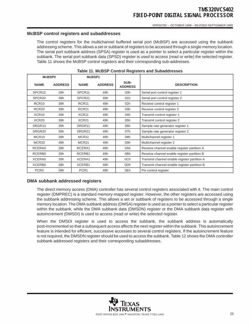
McBSP control registers and subaddresses
The control registers for the multichannel buffered serial port (McBSP) are accessed using the subbankaddressing scheme. This allows a set or subbank of registers to be accessed through a single memory location.The serial port subbank address (SPSA) register is used as a pointer to select a particular register within thesubbank. The serial port subbank data (SPSD) register is used to access (read or write) the selected register.Table 11 shows the McBSP control registers and their corresponding sub-addresses.
Table 11. McBSP Control Registers and SubaddressesMcBSP0 McBSP1
NAME ADDRESS NAME ADDRESSSUB-
ADDRESS DESCRIPTION
ÁÁÁÁÁÁÁÁÁÁ
SPCR10 ÁÁÁÁÁÁÁÁ
39h ÁÁÁÁÁÁÁÁÁÁ
SPCR11 ÁÁÁÁÁÁÁÁ
49h ÁÁÁÁÁÁÁÁÁÁ
00h ÁÁÁÁÁÁÁÁÁÁÁÁÁÁÁÁÁÁÁÁÁÁÁÁÁÁÁÁÁÁ
Serial port control register 1
ÁÁÁÁÁSPCR20 ÁÁÁÁ39h ÁÁÁÁÁSPCR21 ÁÁÁÁ49h ÁÁÁÁÁ01h ÁÁÁÁÁÁÁÁÁÁÁÁÁÁÁSerial port control register 2ÁÁÁÁÁÁÁÁÁÁRCR10
ÁÁÁÁÁÁÁÁ39h
ÁÁÁÁÁÁÁÁÁÁRCR11
ÁÁÁÁÁÁÁÁ49h
ÁÁÁÁÁÁÁÁÁÁ02h
ÁÁÁÁÁÁÁÁÁÁÁÁÁÁÁÁÁÁÁÁÁÁÁÁÁÁÁÁÁÁReceive control register 1ÁÁÁÁÁ
ÁÁÁÁÁRCR20ÁÁÁÁÁÁÁÁ39h
ÁÁÁÁÁÁÁÁÁÁRCR21
ÁÁÁÁÁÁÁÁ49h
ÁÁÁÁÁÁÁÁÁÁ03h
ÁÁÁÁÁÁÁÁÁÁÁÁÁÁÁÁÁÁÁÁÁÁÁÁÁÁÁÁÁÁReceive control register 2ÁÁÁÁÁ
ÁÁÁÁÁXCR10
ÁÁÁÁÁÁÁÁ
39hÁÁÁÁÁÁÁÁÁÁ
XCR11ÁÁÁÁÁÁÁÁ
49hÁÁÁÁÁÁÁÁÁÁ
04hÁÁÁÁÁÁÁÁÁÁÁÁÁÁÁÁÁÁÁÁÁÁÁÁÁÁÁÁÁÁ
Transmit control register 1ÁÁÁÁÁÁÁÁÁÁ
XCR20 ÁÁÁÁÁÁÁÁ
39h ÁÁÁÁÁÁÁÁÁÁ
XCR21 ÁÁÁÁÁÁÁÁ
49h ÁÁÁÁÁÁÁÁÁÁ
05h ÁÁÁÁÁÁÁÁÁÁÁÁÁÁÁÁÁÁÁÁÁÁÁÁÁÁÁÁÁÁ
Transmit control register 2ÁÁÁÁÁÁÁÁÁÁ
SRGR10 ÁÁÁÁÁÁÁÁ
39h ÁÁÁÁÁÁÁÁÁÁ
SRGR11 ÁÁÁÁÁÁÁÁ
49h ÁÁÁÁÁÁÁÁÁÁ
06h ÁÁÁÁÁÁÁÁÁÁÁÁÁÁÁÁÁÁÁÁÁÁÁÁÁÁÁÁÁÁ
Sample rate generator register 1
ÁÁÁÁÁÁÁÁÁÁ
SRGR20 ÁÁÁÁÁÁÁÁ
39h ÁÁÁÁÁÁÁÁÁÁ
SRGR21 ÁÁÁÁÁÁÁÁ
49h ÁÁÁÁÁÁÁÁÁÁ
07h ÁÁÁÁÁÁÁÁÁÁÁÁÁÁÁÁÁÁÁÁÁÁÁÁÁÁÁÁÁÁ
Sample rate generator register 2
ÁÁÁÁÁÁÁÁÁÁ
MCR10 ÁÁÁÁÁÁÁÁ
39h ÁÁÁÁÁÁÁÁÁÁ
MCR11 ÁÁÁÁÁÁÁÁ
49h ÁÁÁÁÁÁÁÁÁÁ
08h ÁÁÁÁÁÁÁÁÁÁÁÁÁÁÁÁÁÁÁÁÁÁÁÁÁÁÁÁÁÁ
Multichannel register 1
ÁÁÁÁÁÁÁÁÁÁ
MCR20 ÁÁÁÁÁÁÁÁ
39h ÁÁÁÁÁÁÁÁÁÁ
MCR21 ÁÁÁÁÁÁÁÁ
49h ÁÁÁÁÁÁÁÁÁÁ
09h ÁÁÁÁÁÁÁÁÁÁÁÁÁÁÁÁÁÁÁÁÁÁÁÁÁÁÁÁÁÁ
Multichannel register 2
ÁÁÁÁÁRCERA0 ÁÁÁÁ39h ÁÁÁÁÁRCERA1 ÁÁÁÁ49h ÁÁÁÁÁ0Ah ÁÁÁÁÁÁÁÁÁÁÁÁÁÁÁReceive channel enable register partition AÁÁÁÁÁÁÁÁÁÁRCERB0
ÁÁÁÁÁÁÁÁ39h
ÁÁÁÁÁÁÁÁÁÁRCERB1
ÁÁÁÁÁÁÁÁ49h
ÁÁÁÁÁÁÁÁÁÁ0Bh
ÁÁÁÁÁÁÁÁÁÁÁÁÁÁÁÁÁÁÁÁÁÁÁÁÁÁÁÁÁÁReceive channel enable register partition BÁÁÁÁÁ
ÁÁÁÁÁXCERA0
ÁÁÁÁÁÁÁÁ
39hÁÁÁÁÁÁÁÁÁÁ
XCERA1ÁÁÁÁÁÁÁÁ
49hÁÁÁÁÁÁÁÁÁÁ
0ChÁÁÁÁÁÁÁÁÁÁÁÁÁÁÁÁÁÁÁÁÁÁÁÁÁÁÁÁÁÁ
Transmit channel enable register partition AÁÁÁÁÁÁÁÁÁÁ
XCERB0ÁÁÁÁÁÁÁÁ
39hÁÁÁÁÁÁÁÁÁÁ
XCERB1ÁÁÁÁÁÁÁÁ
49hÁÁÁÁÁÁÁÁÁÁ
0DhÁÁÁÁÁÁÁÁÁÁÁÁÁÁÁÁÁÁÁÁÁÁÁÁÁÁÁÁÁÁ
Transmit channel enable register partition BÁÁÁÁÁÁÁÁÁÁ
PCR0 ÁÁÁÁÁÁÁÁ
39h ÁÁÁÁÁÁÁÁÁÁ
PCR1 ÁÁÁÁÁÁÁÁ
49h ÁÁÁÁÁÁÁÁÁÁ
0Eh ÁÁÁÁÁÁÁÁÁÁÁÁÁÁÁÁÁÁÁÁÁÁÁÁÁÁÁÁÁÁ
Pin control register
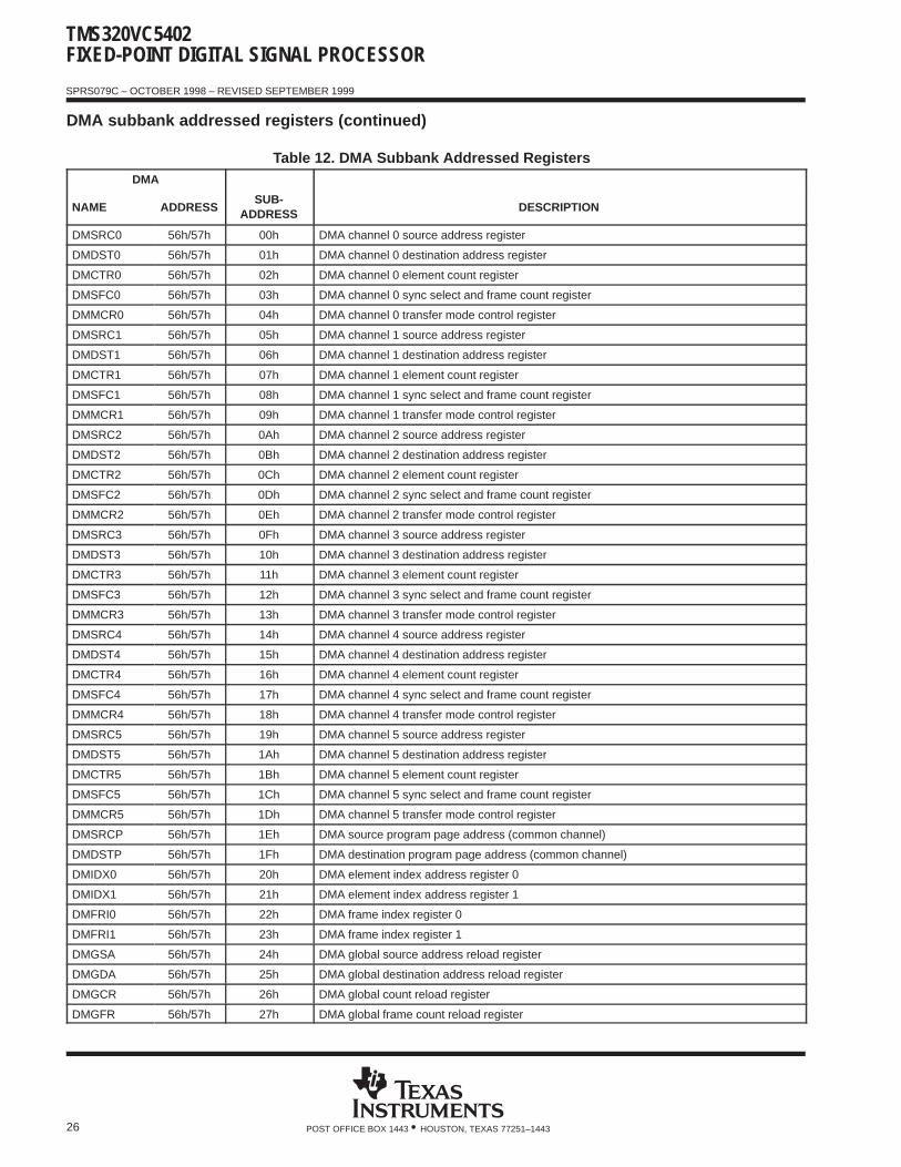
DMA subbank addressed registers
The direct memory access (DMA) controller has several control registers associated with it. The main controlregister (DMPREC) is a standard memory-mapped register. However, the other registers are accessed usingthe subbank addressing scheme. This allows a set or subbank of registers to be accessed through a singlememory location. The DMA subbank address (DMSA) register is used as a pointer to select a particular registerwithin the subbank, while the DMA subbank data (DMSDN) register or the DMA subbank data register withautoincrement (DMSDI) is used to access (read or write) the selected register.
When the DMSDI register is used to access the subbank, the subbank address is automaticallypost-incremented so that a subsequent access affects the next register within the subbank. This autoincrementfeature is intended for efficient, successive accesses to several control registers. If the autoincrement featureis not required, the DMSDN register should be used to access the subbank. Table 12 shows the DMA controllersubbank addressed registers and their corresponding subaddresses.
TMS320VC5402FIXED-POINT DIGITAL SIGNAL PROCESSOR
SPRS079C – OCTOBER 1998 – REVISED SEPTEMBER 1999
26 POST OFFICE BOX 1443 • HOUSTON, TEXAS 77251–1443
DMA subbank addressed registers (continued)
Table 12. DMA Subbank Addressed Registers DMA
NAME ADDRESSSUB-
ADDRESS DESCRIPTION
DMSRC0 56h/57hÁÁÁÁÁÁÁÁÁÁ00h DMA channel 0 source address register
DMDST0 56h/57hÁÁÁÁÁÁÁÁÁÁ
01h DMA channel 0 destination address register
DMCTR0 56h/57hÁÁÁÁÁÁÁÁÁÁ
02h DMA channel 0 element count registerÁÁÁÁÁÁÁÁÁÁ
DMSFC0 ÁÁÁÁÁÁÁÁ
56h/57hÁÁÁÁÁÁÁÁÁÁ
03h ÁÁÁÁÁÁÁÁÁÁÁÁÁÁÁÁÁÁÁÁÁÁÁÁÁÁÁÁÁÁÁÁÁÁÁÁÁÁÁÁÁÁÁÁÁÁ
DMA channel 0 sync select and frame count register
ÁÁÁÁÁÁÁÁÁÁ
DMMCR0 ÁÁÁÁÁÁÁÁ
56h/57hÁÁÁÁÁÁÁÁÁÁ
04h ÁÁÁÁÁÁÁÁÁÁÁÁÁÁÁÁÁÁÁÁÁÁÁÁÁÁÁÁÁÁÁÁÁÁÁÁÁÁÁÁÁÁÁÁÁÁ
DMA channel 0 transfer mode control register
ÁÁÁÁÁÁÁÁÁÁ
DMSRC1 ÁÁÁÁÁÁÁÁ
56h/57hÁÁÁÁÁÁÁÁÁÁ
05h ÁÁÁÁÁÁÁÁÁÁÁÁÁÁÁÁÁÁÁÁÁÁÁÁÁÁÁÁÁÁÁÁÁÁÁÁÁÁÁÁÁÁÁÁÁÁ
DMA channel 1 source address register
ÁÁÁÁÁÁÁÁÁÁ
DMDST1 ÁÁÁÁÁÁÁÁ
56h/57hÁÁÁÁÁÁÁÁÁÁ
06h ÁÁÁÁÁÁÁÁÁÁÁÁÁÁÁÁÁÁÁÁÁÁÁÁÁÁÁÁÁÁÁÁÁÁÁÁÁÁÁÁÁÁÁÁÁÁ
DMA channel 1 destination address register
ÁÁÁÁÁÁÁÁÁÁ
DMCTR1 ÁÁÁÁÁÁÁÁ
56h/57hÁÁÁÁÁÁÁÁÁÁ
07h ÁÁÁÁÁÁÁÁÁÁÁÁÁÁÁÁÁÁÁÁÁÁÁÁÁÁÁÁÁÁÁÁÁÁÁÁÁÁÁÁÁÁÁÁÁÁ
DMA channel 1 element count register
ÁÁÁÁÁDMSFC1 ÁÁÁÁ56h/57hÁÁÁÁÁ08h ÁÁÁÁÁÁÁÁÁÁÁÁÁÁÁÁÁÁÁÁÁÁÁDMA channel 1 sync select and frame count registerÁÁÁÁÁÁÁÁÁÁDMMCR1
ÁÁÁÁÁÁÁÁ56h/57h
ÁÁÁÁÁÁÁÁÁÁ09h
ÁÁÁÁÁÁÁÁÁÁÁÁÁÁÁÁÁÁÁÁÁÁÁÁÁÁÁÁÁÁÁÁÁÁÁÁÁÁÁÁÁÁÁÁÁÁDMA channel 1 transfer mode control registerÁÁÁÁÁ
ÁÁÁÁÁDMSRC2
ÁÁÁÁÁÁÁÁ
56h/57hÁÁÁÁÁÁÁÁÁÁ
0AhÁÁÁÁÁÁÁÁÁÁÁÁÁÁÁÁÁÁÁÁÁÁÁÁÁÁÁÁÁÁÁÁÁÁÁÁÁÁÁÁÁÁÁÁÁÁ
DMA channel 2 source address registerÁÁÁÁÁÁÁÁÁÁ
DMDST2ÁÁÁÁÁÁÁÁ
56h/57hÁÁÁÁÁÁÁÁÁÁ
0BhÁÁÁÁÁÁÁÁÁÁÁÁÁÁÁÁÁÁÁÁÁÁÁÁÁÁÁÁÁÁÁÁÁÁÁÁÁÁÁÁÁÁÁÁÁÁ
DMA channel 2 destination address registerÁÁÁÁÁÁÁÁÁÁ
DMCTR2 ÁÁÁÁÁÁÁÁ
56h/57hÁÁÁÁÁÁÁÁÁÁ
0Ch ÁÁÁÁÁÁÁÁÁÁÁÁÁÁÁÁÁÁÁÁÁÁÁÁÁÁÁÁÁÁÁÁÁÁÁÁÁÁÁÁÁÁÁÁÁÁ
DMA channel 2 element count register
ÁÁÁÁÁÁÁÁÁÁ
DMSFC2 ÁÁÁÁÁÁÁÁ
56h/57hÁÁÁÁÁÁÁÁÁÁ
0Dh ÁÁÁÁÁÁÁÁÁÁÁÁÁÁÁÁÁÁÁÁÁÁÁÁÁÁÁÁÁÁÁÁÁÁÁÁÁÁÁÁÁÁÁÁÁÁ
DMA channel 2 sync select and frame count register
ÁÁÁÁÁÁÁÁÁÁ
DMMCR2 ÁÁÁÁÁÁÁÁ
56h/57hÁÁÁÁÁÁÁÁÁÁ
0Eh ÁÁÁÁÁÁÁÁÁÁÁÁÁÁÁÁÁÁÁÁÁÁÁÁÁÁÁÁÁÁÁÁÁÁÁÁÁÁÁÁÁÁÁÁÁÁ
DMA channel 2 transfer mode control register
ÁÁÁÁÁÁÁÁÁÁ
DMSRC3 ÁÁÁÁÁÁÁÁ
56h/57hÁÁÁÁÁÁÁÁÁÁ
0Fh ÁÁÁÁÁÁÁÁÁÁÁÁÁÁÁÁÁÁÁÁÁÁÁÁÁÁÁÁÁÁÁÁÁÁÁÁÁÁÁÁÁÁÁÁÁÁ
DMA channel 3 source address register
ÁÁÁÁÁDMDST3 ÁÁÁÁ56h/57hÁÁÁÁÁ10h ÁÁÁÁÁÁÁÁÁÁÁÁÁÁÁÁÁÁÁÁÁÁÁDMA channel 3 destination address registerÁÁÁÁÁÁÁÁÁÁDMCTR3
ÁÁÁÁÁÁÁÁ56h/57h
ÁÁÁÁÁÁÁÁÁÁ11h
ÁÁÁÁÁÁÁÁÁÁÁÁÁÁÁÁÁÁÁÁÁÁÁÁÁÁÁÁÁÁÁÁÁÁÁÁÁÁÁÁÁÁÁÁÁÁDMA channel 3 element count registerÁÁÁÁÁ
ÁÁÁÁÁDMSFC3
ÁÁÁÁÁÁÁÁ
56h/57hÁÁÁÁÁÁÁÁÁÁ
12hÁÁÁÁÁÁÁÁÁÁÁÁÁÁÁÁÁÁÁÁÁÁÁÁÁÁÁÁÁÁÁÁÁÁÁÁÁÁÁÁÁÁÁÁÁÁ
DMA channel 3 sync select and frame count registerÁÁÁÁÁÁÁÁÁÁ
DMMCR3ÁÁÁÁÁÁÁÁ
56h/57hÁÁÁÁÁÁÁÁÁÁ
13hÁÁÁÁÁÁÁÁÁÁÁÁÁÁÁÁÁÁÁÁÁÁÁÁÁÁÁÁÁÁÁÁÁÁÁÁÁÁÁÁÁÁÁÁÁÁ
DMA channel 3 transfer mode control registerÁÁÁÁÁÁÁÁÁÁ
DMSRC4 ÁÁÁÁÁÁÁÁ
56h/57hÁÁÁÁÁÁÁÁÁÁ
14h ÁÁÁÁÁÁÁÁÁÁÁÁÁÁÁÁÁÁÁÁÁÁÁÁÁÁÁÁÁÁÁÁÁÁÁÁÁÁÁÁÁÁÁÁÁÁ
DMA channel 4 source address register
ÁÁÁÁÁÁÁÁÁÁ
DMDST4 ÁÁÁÁÁÁÁÁ
56h/57hÁÁÁÁÁÁÁÁÁÁ
15h ÁÁÁÁÁÁÁÁÁÁÁÁÁÁÁÁÁÁÁÁÁÁÁÁÁÁÁÁÁÁÁÁÁÁÁÁÁÁÁÁÁÁÁÁÁÁ
DMA channel 4 destination address register
ÁÁÁÁÁÁÁÁÁÁ
DMCTR4 ÁÁÁÁÁÁÁÁ
56h/57hÁÁÁÁÁÁÁÁÁÁ
16h ÁÁÁÁÁÁÁÁÁÁÁÁÁÁÁÁÁÁÁÁÁÁÁÁÁÁÁÁÁÁÁÁÁÁÁÁÁÁÁÁÁÁÁÁÁÁ
DMA channel 4 element count register
ÁÁÁÁÁÁÁÁÁÁ
DMSFC4 ÁÁÁÁÁÁÁÁ
56h/57hÁÁÁÁÁÁÁÁÁÁ
17h ÁÁÁÁÁÁÁÁÁÁÁÁÁÁÁÁÁÁÁÁÁÁÁÁÁÁÁÁÁÁÁÁÁÁÁÁÁÁÁÁÁÁÁÁÁÁ
DMA channel 4 sync select and frame count register
ÁÁÁÁÁÁÁÁÁÁ
DMMCR4 ÁÁÁÁÁÁÁÁ
56h/57hÁÁÁÁÁÁÁÁÁÁ
18h ÁÁÁÁÁÁÁÁÁÁÁÁÁÁÁÁÁÁÁÁÁÁÁÁÁÁÁÁÁÁÁÁÁÁÁÁÁÁÁÁÁÁÁÁÁÁ
DMA channel 4 transfer mode control register
ÁÁÁÁÁDMSRC5 ÁÁÁÁ56h/57hÁÁÁÁÁ19h ÁÁÁÁÁÁÁÁÁÁÁÁÁÁÁÁÁÁÁÁÁÁÁDMA channel 5 source address registerÁÁÁÁÁÁÁÁÁÁDMDST5
ÁÁÁÁÁÁÁÁ56h/57h
ÁÁÁÁÁÁÁÁÁÁ1Ah
ÁÁÁÁÁÁÁÁÁÁÁÁÁÁÁÁÁÁÁÁÁÁÁÁÁÁÁÁÁÁÁÁÁÁÁÁÁÁÁÁÁÁÁÁÁÁDMA channel 5 destination address registerÁÁÁÁÁ
ÁÁÁÁÁDMCTR5
ÁÁÁÁÁÁÁÁ
56h/57hÁÁÁÁÁÁÁÁÁÁ
1BhÁÁÁÁÁÁÁÁÁÁÁÁÁÁÁÁÁÁÁÁÁÁÁÁÁÁÁÁÁÁÁÁÁÁÁÁÁÁÁÁÁÁÁÁÁÁ
DMA channel 5 element count registerÁÁÁÁÁÁÁÁÁÁ
DMSFC5ÁÁÁÁÁÁÁÁ
56h/57hÁÁÁÁÁÁÁÁÁÁ
1ChÁÁÁÁÁÁÁÁÁÁÁÁÁÁÁÁÁÁÁÁÁÁÁÁÁÁÁÁÁÁÁÁÁÁÁÁÁÁÁÁÁÁÁÁÁÁ
DMA channel 5 sync select and frame count registerÁÁÁÁÁÁÁÁÁÁ
DMMCR5 ÁÁÁÁÁÁÁÁ
56h/57hÁÁÁÁÁÁÁÁÁÁ
1Dh ÁÁÁÁÁÁÁÁÁÁÁÁÁÁÁÁÁÁÁÁÁÁÁÁÁÁÁÁÁÁÁÁÁÁÁÁÁÁÁÁÁÁÁÁÁÁ
DMA channel 5 transfer mode control register
ÁÁÁÁÁÁÁÁÁÁ
DMSRCP ÁÁÁÁÁÁÁÁ
56h/57hÁÁÁÁÁÁÁÁÁÁ
1Eh ÁÁÁÁÁÁÁÁÁÁÁÁÁÁÁÁÁÁÁÁÁÁÁÁÁÁÁÁÁÁÁÁÁÁÁÁÁÁÁÁÁÁÁÁÁÁ
DMA source program page address (common channel)
ÁÁÁÁÁÁÁÁÁÁ
DMDSTP ÁÁÁÁÁÁÁÁ
56h/57hÁÁÁÁÁÁÁÁÁÁ
1Fh ÁÁÁÁÁÁÁÁÁÁÁÁÁÁÁÁÁÁÁÁÁÁÁÁÁÁÁÁÁÁÁÁÁÁÁÁÁÁÁÁÁÁÁÁÁÁ
DMA destination program page address (common channel)
ÁÁÁÁÁÁÁÁÁÁ
DMIDX0 ÁÁÁÁÁÁÁÁ
56h/57hÁÁÁÁÁÁÁÁÁÁ
20h ÁÁÁÁÁÁÁÁÁÁÁÁÁÁÁÁÁÁÁÁÁÁÁÁÁÁÁÁÁÁÁÁÁÁÁÁÁÁÁÁÁÁÁÁÁÁ
DMA element index address register 0
ÁÁÁÁÁDMIDX1 ÁÁÁÁ56h/57hÁÁÁÁÁ21h ÁÁÁÁÁÁÁÁÁÁÁÁÁÁÁÁÁÁÁÁÁÁÁDMA element index address register 1ÁÁÁÁÁÁÁÁÁÁDMFRI0
ÁÁÁÁÁÁÁÁ56h/57h
ÁÁÁÁÁÁÁÁÁÁ22h
ÁÁÁÁÁÁÁÁÁÁÁÁÁÁÁÁÁÁÁÁÁÁÁÁÁÁÁÁÁÁÁÁÁÁÁÁÁÁÁÁÁÁÁÁÁÁDMA frame index register 0ÁÁÁÁÁ
ÁÁÁÁÁDMFRI1
ÁÁÁÁÁÁÁÁ
56h/57hÁÁÁÁÁÁÁÁÁÁ
23hÁÁÁÁÁÁÁÁÁÁÁÁÁÁÁÁÁÁÁÁÁÁÁÁÁÁÁÁÁÁÁÁÁÁÁÁÁÁÁÁÁÁÁÁÁÁ
DMA frame index register 1ÁÁÁÁÁÁÁÁÁÁ
DMGSAÁÁÁÁÁÁÁÁ
56h/57hÁÁÁÁÁÁÁÁÁÁ
24hÁÁÁÁÁÁÁÁÁÁÁÁÁÁÁÁÁÁÁÁÁÁÁÁÁÁÁÁÁÁÁÁÁÁÁÁÁÁÁÁÁÁÁÁÁÁ
DMA global source address reload registerÁÁÁÁÁÁÁÁÁÁ
DMGDA ÁÁÁÁÁÁÁÁ
56h/57hÁÁÁÁÁÁÁÁÁÁ
25h ÁÁÁÁÁÁÁÁÁÁÁÁÁÁÁÁÁÁÁÁÁÁÁÁÁÁÁÁÁÁÁÁÁÁÁÁÁÁÁÁÁÁÁÁÁÁ
DMA global destination address reload register
ÁÁÁÁÁÁÁÁÁÁ
DMGCR ÁÁÁÁÁÁÁÁ
56h/57hÁÁÁÁÁÁÁÁÁÁ
26h ÁÁÁÁÁÁÁÁÁÁÁÁÁÁÁÁÁÁÁÁÁÁÁÁÁÁÁÁÁÁÁÁÁÁÁÁÁÁÁÁÁÁÁÁÁÁ
DMA global count reload register
ÁÁÁÁÁÁÁÁÁÁ
DMGFR ÁÁÁÁÁÁÁÁ
56h/57hÁÁÁÁÁÁÁÁÁÁ
27h ÁÁÁÁÁÁÁÁÁÁÁÁÁÁÁÁÁÁÁÁÁÁÁÁÁÁÁÁÁÁÁÁÁÁÁÁÁÁÁÁÁÁÁÁÁÁ
DMA global frame count reload register
TMS320VC5402FIXED-POINT DIGITAL SIGNAL PROCESSOR
SPRS079C – OCTOBER 1998 – REVISED SEPTEMBER 1999
27POST OFFICE BOX 1443 • HOUSTON, TEXAS 77251–1443
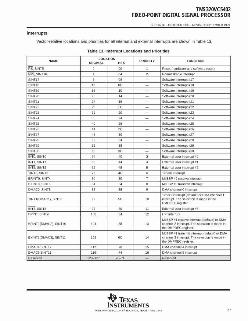
interrupts
Vector-relative locations and priorities for all internal and external interrupts are shown in Table 13.
Table 13. Interrupt Locations and Priorities
NAMELOCATION
DECIMAL HEX PRIORITY FUNCTION
RS, SINTR 0 00 1 Reset (hardware and software reset)
NMI, SINT16 4 04 2 Nonmaskable interrupt
SINT17 8 08 — Software interrupt #17
SINT18 12 0C — Software interrupt #18
SINT19 16 10 — Software interrupt #19
SINT20 20 14 — Software interrupt #20
SINT21 24 18 — Software interrupt #21
SINT22 28 1C — Software interrupt #22
SINT23 32 20 — Software interrupt #23
SINT24 36 24 — Software interrupt #24
SINT25 40 28 — Software interrupt #25
SINT26 44 2C — Software interrupt #26
SINT27 48 30 — Software interrupt #27
SINT28 52 34 — Software interrupt #28
SINT29 56 38 — Software interrupt #29
SINT30 60 3C — Software interrupt #30
INT0, SINT0 64 40 3 External user interrupt #0
INT1, SINT1 68 44 4 External user interrupt #1
INT2, SINT2 72 48 5 External user interrupt #2
TINT0, SINT3 76 4C 6 Timer0 interrupt
BRINT0, SINT4 80 50 7 McBSP #0 receive interrupt
BXINT0, SINT5 84 54 8 McBSP #0 transmit interrupt
DMAC0, SINT6 88 58 9 DMA channel 0 interrupt
TINT1(DMAC1), SINT7 92 5C 10Timer1 interrupt (default) or DMA channel 1interrupt. The selection is made in theDMPREC register.
INT3, SINT8 96 60 11 External user interrupt #3
HPINT, SINT9 100 64 12 HPI interrupt
BRINT1(DMAC2), SINT10 104 68 13McBSP #1 receive interrupt (default) or DMAchannel 2 interrupt. The selection is made inthe DMPREC register.
BXINT1(DMAC3), SINT11 108 6C 14McBSP #1 transmit interrupt (default) or DMAchannel 3 interrupt. The selection is made inthe DMPREC register.
DMAC4,SINT12 112 70 15 DMA channel 4 interrupt
DMAC5,SINT13 116 74 16 DMA channel 5 interrupt
Reserved 120–127 78–7F — Reserved
TMS320VC5402FIXED-POINT DIGITAL SIGNAL PROCESSOR
SPRS079C – OCTOBER 1998 – REVISED SEPTEMBER 1999
28 POST OFFICE BOX 1443 • HOUSTON, TEXAS 77251–1443
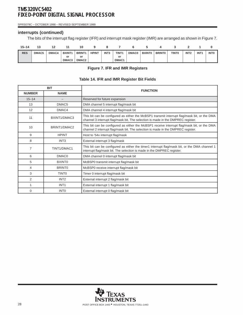
interrupts (continued)The bits of the interrupt flag register (IFR) and interrupt mask register (IMR) are arranged as shown in Figure 7.
15–14 13 12 11 10 9 8 7 6 5 4 3 2 1 0
RES DMAC5 DMAC4 BXINT1or
DMAC3
BRINT1or
DMAC2
HPINT INT3 TINT1or
DMAC1
DMAC0 BXINT0 BRINT0 TINT0 INT2 INT1 INT0
Figure 7. IFR and IMR Registers
Table 14. IFR and IMR Register Bit Fields
BITFUNCTION
NUMBER NAMEFUNCTION
15–14 – Reserved for future expansion
13 DMAC5 DMA channel 5 interrupt flag/mask bit
12 DMAC4 DMA channel 4 interrupt flag/mask bit
11 BXINT1/DMAC3 This bit can be configured as either the McBSP1 transmit interrupt flag/mask bit, or the DMAchannel 3 interrupt flag/mask bit. The selection is made in the DMPREC register.
10 BRINT1/DMAC2 This bit can be configured as either the McBSP1 receive interrupt flag/mask bit, or the DMAchannel 2 interrupt flag/mask bit. The selection is made in the DMPREC register.
9 HPINT Host to ’54x interrupt flag/mask
8 INT3 External interrupt 3 flag/mask
7 TINT1/DMAC1 This bit can be configured as either the timer1 interrupt flag/mask bit, or the DMA channel 1interrupt flag/mask bit. The selection is made in the DMPREC register.
6 DMAC0 DMA channel 0 interrupt flag/mask bit
5 BXINT0 McBSP0 transmit interrupt flag/mask bit
4 BRINT0 McBSP0 receive interrupt flag/mask bit
3 TINT0 Timer 0 interrupt flag/mask bit
2 INT2 External interrupt 2 flag/mask bit
1 INT1 External interrupt 1 flag/mask bit
0 INT0 External interrupt 0 flag/mask bit
TMS320VC5402FIXED-POINT DIGITAL SIGNAL PROCESSOR
SPRS079C – OCTOBER 1998 – REVISED SEPTEMBER 1999
29POST OFFICE BOX 1443 • HOUSTON, TEXAS 77251–1443
documentation support
Extensive documentation supports all TMS320 family generations of devices from product announcementthrough applications development. The following types of documentation are available to support the designand use of the ’C5000 family of DSPs:
TMS320C5000 DSP Family Functional Overview (literature number SPRU307) Device-specific data sheets (such as this document) Complete User Guides Development-support tools Hardware and software application reports
The five-volume TMS320C54x DSP Reference Set (literature number SPRU210) consists of:
Volume 1: CPU and Peripherals (literature number SPRU131) Volume 2: Mnemonic Instruction Set (literature number SPRU172) Volume 3: Algebraic Instruction Set (literature number SPRU179) Volume 4: Applications Guide (literature number SPRU173) Volume 5: Enhanced Peripherals (literature number SPRU302)
The reference set describes in detail the ’54x TMS320 products currently available and the hardware andsoftware applications, including algorithms, for fixed-point TMS320 devices.
For general background information on DSPs and Texas Instruments (TI) devices, see the three-volumepublication Digital Signal Processing Applications with the TMS320 Family (literature numbers SPRA012,SPRA016, and SPRA017).
A series of DSP textbooks is published by Prentice-Hall and John Wiley & Sons to support digital signalprocessing research and education. The TMS320 newsletter, Details on Signal Processing, is publishedquarterly and distributed to update TMS320 customers on product information.
Information regarding TI DSP products is also available on the Worldwide Web at http://www.ti.com uniformresource locator (URL).
TI is a trademark of Texas Instruments Incorporated.

TMS320VC5402FIXED-POINT DIGITAL SIGNAL PROCESSOR
SPRS079C – OCTOBER 1998 – REVISED SEPTEMBER 1999
30 POST OFFICE BOX 1443 • HOUSTON, TEXAS 77251–1443
absolute maximum ratings over specified temperature range (unless otherwise noted) †
Supply voltage I/O range, DVDD‡ –0.3 V to 4.0 V. . . . . . . . . . . . . . . . . . . . . . . . . . . . . . . . . . . . . . . . . . . . . . . . . . . . Supply voltage core range, CVDD‡ –0.3 V to 2.0 V. . . . . . . . . . . . . . . . . . . . . . . . . . . . . . . . . . . . . . . . . . . . . . . . . . Input voltage range, VI –0.3 V to 4.5 V. . . . . . . . . . . . . . . . . . . . . . . . . . . . . . . . . . . . . . . . . . . . . . . . . . . . . . . . . . . . . Output voltage range, VO –0.3 V to 4.5 V. . . . . . . . . . . . . . . . . . . . . . . . . . . . . . . . . . . . . . . . . . . . . . . . . . . . . . . . . . . Operating case temperature range, TC –40°C to 100°C. . . . . . . . . . . . . . . . . . . . . . . . . . . . . . . . . . . . . . . . . . . . . . Storage temperature range, Tstg –55°C to 150°C. . . . . . . . . . . . . . . . . . . . . . . . . . . . . . . . . . . . . . . . . . . . . . . . . . . .
† Stresses beyond those listed under “absolute maximum ratings” may cause permanent damage to the device. These are stress ratings only, andfunctional operation of the device at these or any other conditions beyond those indicated under “recommended operating conditions” is notimplied. Exposure to absolute-maximum-rated conditions for extended periods may affect device reliability.
‡ All voltage values are with respect to VSS.
recommended operating conditions
MIN NOM MAX UNIT
DVDD Device supply voltage, I/O 3 3.3 3.6 V
CVDD Device supply voltage, core 1.71 1.8 1.98 V
VSS Supply voltage, GND 0 V
VIHHigh-level input voltageDV 3 3 0 3 V
RS, INTn, NMI, X2/CLKIN§, BIO, BCLKR0,BCLKR1, BCLKX0, BCLKX1, HCS, HDS1,HDS2, TDI, TMS, CLKMDn
2.2 DVDD + 0.3
VVIH DVDD = 3.30.3 V TCK, TRST 2.5 DVDD + 0.3V
All other inputs 2.0 DVDD + 0.3
VILLow-level input voltageDVDD = 3.30.3 V
RS, INTn, NMI, X2/CLKIN§, BIO, BCLKR0,BCLKR1, BCLKX0, BCLKX1, HCS, HDS1,HDS2, TCK, CLKMDn
–0.3 0.6V
DDAll other inputs –0.3 0.8
IOH High-level output current –300 µA
IOL Low-level output current 1.5 mA
TC Operating case temperature –40 100 °C§ The TMS320VC5402 Rev. B must be operated with the on-chip oscillator. This device does not support operation with an external clock source.
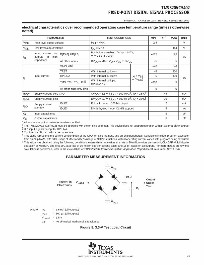
TMS320VC5402FIXED-POINT DIGITAL SIGNAL PROCESSOR
SPRS079C – OCTOBER 1998 – REVISED SEPTEMBER 1999
31POST OFFICE BOX 1443 • HOUSTON, TEXAS 77251–1443
electrical characteristics over recommended operating case temperature range (unless otherwisenoted)
PARAMETER TEST CONDITIONS MIN TYP† MAX UNIT
VOH High-level output voltage IOH = MAX 2.4 V
VOL Low-level output voltage IOL = MAX 0.4 V
IIZ
Input current foroutputs in high
D[15:0], HD[7:0]Bus holders enabled, DVDD = MAX,VI = VSS to DVDD
–175 175µAIZ
impedance All other inputs DVDD = MAX, VO = VSS to DVDD –5 5
µ
X2/CLKIN –40 40
TRST With internal pulldown –5 300
IIInput current HPIENA With internal pulldown (VI = VSS –5 300
µAIITMS, TCK, TDI, HPI
With internal pullups, HPIENA = 0
to DVDD)–300 5
µA
All other input only pins 5 5All other input-only pins –5 5
IDDC Supply current, core CPU CVDD = 1.8 V, fclock = 100 MHz¶, TC = 25°C# 45 mA
IDDP Supply current, pins DVDD = 3.3 V, fclock = 100 MHz¶, TC = 25°C|| 30 mA
IDDSupply current, IDLE2 PLL × 1 mode, 100 MHz input 2 mA
IDDy
standby IDLE3 Divide-by-two mode, CLKIN stopped 5 µA
Ci Input capacitance 5 pF
Co Output capacitance 5 pF† All values are typical unless otherwise specified.‡ The TMS320VC5402 Rev. B must be operated with the on-chip oscillator. This device does not support operation with an external clock source.§ HPI input signals except for HPIENA.¶ Clock mode: PLL × 1 with external source# This value represents the current consumption of the CPU, on-chip memory, and on-chip peripherals. Conditions include: program execution
from on-chip RAM, with 50% usage of MAC and 50% usage of NOP instructions. Actual operating current varies with program being executed.|| This value was obtained using the following conditions: external memory writes at a rate of 20 million writes per second, CLKOFF=0, full-duplex
operation of McBSP0 and McBSP1 at a rate of 10 million bits per second each, and 15-pF loads on all outputs. For more details on how thiscalculation is performed, refer to the Calculation of TMS320C54x Power Dissipation Application Report (literature number SPRA164).
PARAMETER MEASUREMENT INFORMATION
Tester PinElectronics
VLoad
IOL
CT
IOH
OutputUnderTest
50 Ω
Where: IOL = 1.5 mA (all outputs)
IOH = 300 µA (all outputs)
VLoad = 1.5 V
CT = 40 pF typical load circuit capacitance
Figure 8. 3.3-V Test Load Circuit
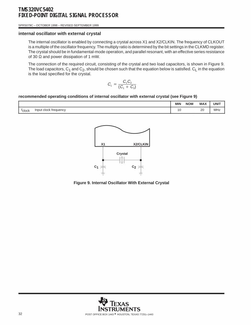
TMS320VC5402FIXED-POINT DIGITAL SIGNAL PROCESSOR
SPRS079C – OCTOBER 1998 – REVISED SEPTEMBER 1999
32 POST OFFICE BOX 1443 • HOUSTON, TEXAS 77251–1443
internal oscillator with external crystal
The internal oscillator is enabled by connecting a crystal across X1 and X2/CLKIN. The frequency of CLKOUTis a multiple of the oscillator frequency. The multiply ratio is determined by the bit settings in the CLKMD register.The crystal should be in fundamental-mode operation, and parallel resonant, with an effective series resistanceof 30 Ω and power dissipation of 1 mW.
The connection of the required circuit, consisting of the crystal and two load capacitors, is shown in Figure 9.The load capacitors, C1 and C2, should be chosen such that the equation below is satisfied. CL in the equationis the load specified for the crystal.
CLC1C2
(C1C2)
recommended operating conditions of internal oscillator with external crystal (see Figure 9)
MIN NOM MAX UNIT
fclock Input clock frequency 10 20 MHz
X1 X2/CLKIN
C1 C2
Crystal
Figure 9. Internal Oscillator With External Crystal
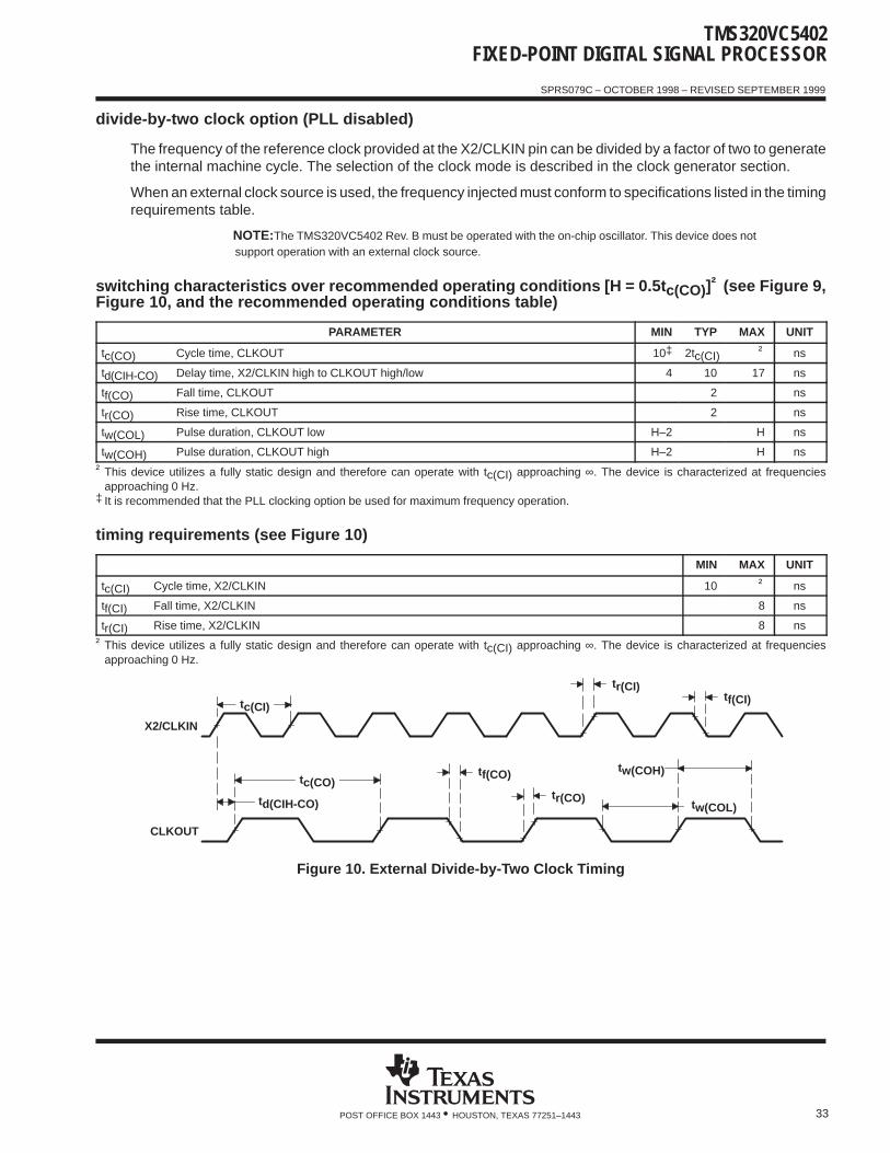
TMS320VC5402FIXED-POINT DIGITAL SIGNAL PROCESSOR
SPRS079C – OCTOBER 1998 – REVISED SEPTEMBER 1999
33POST OFFICE BOX 1443 • HOUSTON, TEXAS 77251–1443
divide-by-two clock option (PLL disabled)
The frequency of the reference clock provided at the X2/CLKIN pin can be divided by a factor of two to generatethe internal machine cycle. The selection of the clock mode is described in the clock generator section.
When an external clock source is used, the frequency injected must conform to specifications listed in the timingrequirements table.
NOTE:The TMS320VC5402 Rev. B must be operated with the on-chip oscillator. This device does notsupport operation with an external clock source.
switching characteristics over recommended operating conditions [H = 0.5t c(CO)]† (see Figure 9,Figure 10, and the recommended operating conditions table)
PARAMETER MIN TYP MAX UNIT
tc(CO) Cycle time, CLKOUT 10‡ 2tc(CI) † ns
td(CIH-CO) Delay time, X2/CLKIN high to CLKOUT high/low 4 10 17 ns
tf(CO) Fall time, CLKOUT 2 ns
tr(CO) Rise time, CLKOUT 2 ns
tw(COL) Pulse duration, CLKOUT low H–2 H ns
tw(COH) Pulse duration, CLKOUT high H–2 H ns
† This device utilizes a fully static design and therefore can operate with tc(CI) approaching ∞. The device is characterized at frequenciesapproaching 0 Hz.
‡ It is recommended that the PLL clocking option be used for maximum frequency operation.
timing requirements (see Figure 10)
MIN MAX UNIT
tc(CI) Cycle time, X2/CLKIN 10 † ns
tf(CI) Fall time, X2/CLKIN 8 ns
tr(CI) Rise time, X2/CLKIN 8 ns
† This device utilizes a fully static design and therefore can operate with tc(CI) approaching ∞. The device is characterized at frequenciesapproaching 0 Hz.
tr(CO)
tf(CO)
CLKOUT
X2/CLKIN
tw(COL)td(CIH-CO)
tf(CI)tr(CI)
tc(CO)
tc(CI)
tw(COH)
Figure 10. External Divide-by-Two Clock Timing
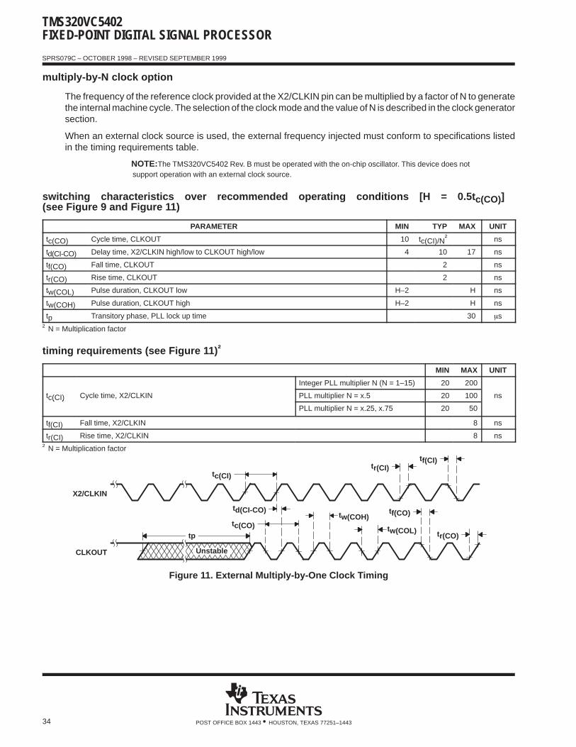
TMS320VC5402FIXED-POINT DIGITAL SIGNAL PROCESSOR
SPRS079C – OCTOBER 1998 – REVISED SEPTEMBER 1999
34 POST OFFICE BOX 1443 • HOUSTON, TEXAS 77251–1443
multiply-by-N clock option
The frequency of the reference clock provided at the X2/CLKIN pin can be multiplied by a factor of N to generatethe internal machine cycle. The selection of the clock mode and the value of N is described in the clock generatorsection.
When an external clock source is used, the external frequency injected must conform to specifications listedin the timing requirements table.
NOTE:The TMS320VC5402 Rev. B must be operated with the on-chip oscillator. This device does notsupport operation with an external clock source.
switching characteristics over recommended operating conditions [H = 0.5t c(CO)] (see Figure 9 and Figure 11)
PARAMETER MIN TYP MAX UNIT
tc(CO) Cycle time, CLKOUT 10 tc(CI)/N† ns
td(CI-CO) Delay time, X2/CLKIN high/low to CLKOUT high/low 4 10 17 ns
tf(CO) Fall time, CLKOUT 2 ns
tr(CO) Rise time, CLKOUT 2 ns
tw(COL) Pulse duration, CLKOUT low H–2 H ns
tw(COH) Pulse duration, CLKOUT high H–2 H ns
tp Transitory phase, PLL lock up time 30 s
† N = Multiplication factor
timing requirements (see Figure 11) †
MIN MAX UNIT
Integer PLL multiplier N (N = 1–15) 20 200
tc(CI) Cycle time, X2/CLKIN PLL multiplier N = x.5 20 100 ns( )PLL multiplier N = x.25, x.75 20 50
tf(CI) Fall time, X2/CLKIN 8 ns
tr(CI) Rise time, X2/CLKIN 8 ns
† N = Multiplication factor
tc(CO)
tc(CI)
tw(COH)tf(CO)
tr(CO)
tf(CI)
X2/CLKIN
CLKOUT
td(CI-CO)
tw(COL)
tr(CI)
tp
Unstable
Figure 11. External Multiply-by-One Clock Timing
TMS320VC5402FIXED-POINT DIGITAL SIGNAL PROCESSOR
SPRS079C – OCTOBER 1998 – REVISED SEPTEMBER 1999
35POST OFFICE BOX 1443 • HOUSTON, TEXAS 77251–1443
memory and parallel I/O interface timing
switching characteristics over recommended operating conditions for a memory read(MSTRB = 0)† (see Figure 12)
PARAMETER MIN MAX UNIT
td(CLKL-A) Delay time, CLKOUT low to address valid‡ –2 3 ns
td(CLKH-A) Delay time, CLKOUT high (transition) to address valid§ –2 3 ns
td(CLKL-MSL) Delay time, CLKOUT low to MSTRB low –1 3 ns
td(CLKL-MSH) Delay time, CLKOUT low to MSTRB high –1 3 ns
th(CLKL-A)R Hold time, address valid after CLKOUT low‡ –2 3 ns
th(CLKH-A)R Hold time, address valid after CLKOUT high§ –2 3 ns
† Address, PS, and DS timings are all included in timings referenced as address.‡ In the case of a memory read preceded by a memory read§ In the case of a memory read preceded by a memory write
timing requirements for a memory read (MSTRB = 0) [H = 0.5 tc(CO)]† (see Figure 12)
MIN MAX UNIT
ta(A)M Access time, read data access from address valid 2H–7 ns
ta(MSTRBL) Access time, read data access from MSTRB low 2H–8 ns
tsu(D)R Setup time, read data before CLKOUT low 6 ns
th(D)R Hold time, read data after CLKOUT low –2 ns
th(A-D)R Hold time, read data after address invalid 0 ns
th(D)MSTRBH Hold time, read data after MSTRB high 0 ns
† Address, PS, and DS timings are all included in timings referenced as address.

TMS320VC5402FIXED-POINT DIGITAL SIGNAL PROCESSOR
SPRS079C – OCTOBER 1998 – REVISED SEPTEMBER 1999
36 POST OFFICE BOX 1443 • HOUSTON, TEXAS 77251–1443
memory and parallel I/O interface timing (continued)
PS, DS
R/W
MSTRB
D[15:0]
A[19:0]
CLKOUT
th(D)R
th(CLKL-A)R
td(CLKL-MSH)
td(CLKL-A)
td(CLKL-MSL)
tsu(D)R
ta(A)M
ta(MSTRBL)
th(A-D)R
th(D)MSTRBH
NOTE A: A[19:16] are always driven low during accesses to external data space.
Figure 12. Memory Read (MSTRB = 0)
TMS320VC5402FIXED-POINT DIGITAL SIGNAL PROCESSOR
SPRS079C – OCTOBER 1998 – REVISED SEPTEMBER 1999
37POST OFFICE BOX 1443 • HOUSTON, TEXAS 77251–1443
memory and parallel I/O interface timing (continued)
switching characteristics over recommended operating conditions for a memory write(MSTRB = 0) [H = 0.5 tc(CO)]† (see Figure 13)
PARAMETER MIN MAX UNIT
td(CLKH-A) Delay time, CLKOUT high to address valid‡ –2 3 ns
td(CLKL-A) Delay time, CLKOUT low to address valid§ –2 3 ns
td(CLKL-MSL) Delay time, CLKOUT low to MSTRB low –1 3 ns
td(CLKL-D)W Delay time, CLKOUT low to data valid 0 6 ns
td(CLKL-MSH) Delay time, CLKOUT low to MSTRB high –1 3 ns
td(CLKH-RWL) Delay time, CLKOUT high to R/W low –1 3 ns
td(CLKH-RWH) Delay time, CLKOUT high to R/W high –1 3 ns
td(RWL-MSTRBL) Delay time, R/W low to MSTRB low H – 2 H + 1 ns
th(A)W Hold time, address valid after CLKOUT high‡ 1 3 ns
th(D)MSH Hold time, write data valid after MSTRB high H–3 H+6§ ns
tw(SL)MS Pulse duration, MSTRB low 2H–2 ns
tsu(A)W Setup time, address valid before MSTRB low 2H–2 ns
tsu(D)MSH Setup time, write data valid before MSTRB high 2H–6 2H+5§ ns
ten(D–RWL) Enable time, data bus driven after R/W low H–5 ns
tdis(RWH–D) Disable time, R/W high to data bus high impedance 0 ns
† Address, PS, and DS timings are all included in timings referenced as address.‡ In the case of a memory write preceded by a memory write§ In the case of a memory write preceded by an I/O cycle
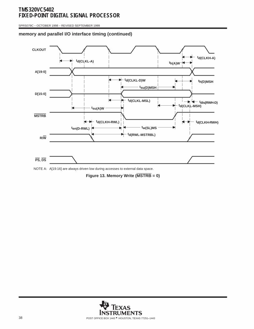
TMS320VC5402FIXED-POINT DIGITAL SIGNAL PROCESSOR
SPRS079C – OCTOBER 1998 – REVISED SEPTEMBER 1999
38 POST OFFICE BOX 1443 • HOUSTON, TEXAS 77251–1443
memory and parallel I/O interface timing (continued)
PS, DS
R/W
MSTRB
D[15:0]
A[19:0]
CLKOUT
td(CLKH-RWH)
th(A)W
td(CLKL-MSH)
tsu(D)MSH
td(CLKL-D)W
tw(SL)MS
tsu(A)W
td(CLKL-MSL)
th(D)MSH
td(CLKL-A)
td(CLKH-RWL)
td(RWL-MSTRBL)
td(CLKH-A)
ten(D-RWL)
tdis(RWH-D)
NOTE A: A[19:16] are always driven low during accesses to external data space.
Figure 13. Memory Write (MSTRB = 0)
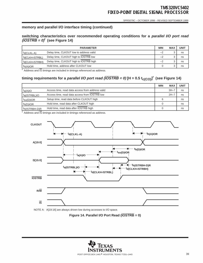
TMS320VC5402FIXED-POINT DIGITAL SIGNAL PROCESSOR
SPRS079C – OCTOBER 1998 – REVISED SEPTEMBER 1999
39POST OFFICE BOX 1443 • HOUSTON, TEXAS 77251–1443
memory and parallel I/O interface timing (continued)
switching characteristics over recommended operating conditions for a parallel I/O port read(IOSTRB = 0)† (see Figure 14)
PARAMETER MIN MAX UNIT
td(CLKL-A) Delay time, CLKOUT low to address valid –2 3 ns
td(CLKH-ISTRBL) Delay time, CLKOUT high to IOSTRB low –2 3 ns
td(CLKH-ISTRBH) Delay time, CLKOUT high to IOSTRB high –2 3 ns
th(A)IOR Hold time, address after CLKOUT low 0 3 ns
† Address and IS timings are included in timings referenced as address.
timing requirements for a parallel I/O port read (IOSTRB = 0) [H = 0.5 tc(CO)]† (see Figure 14)
MIN MAX UNIT
ta(A)IO Access time, read data access from address valid 3H–7 ns
ta(ISTRBL)IO Access time, read data access from IOSTRB low 2H–7 ns
tsu(D)IOR Setup time, read data before CLKOUT high 6 ns
th(D)IOR Hold time, read data after CLKOUT high 0 ns
th(ISTRBH-D)R Hold time, read data after IOSTRB high 0 ns
† Address and IS timings are included in timings referenced as address.
IS
R/W
IOSTRB
D[15:0]
A[19:0]
CLKOUT
th(A)IOR
td(CLKH-ISTRBH)
th(D)IORtsu(D)IOR
ta(A)IO
td(CLKH-ISTRBL)
td(CLKL-A)
ta(ISTRBL)IOth(ISTRBH-D)R
NOTE A: A[19:16] are always driven low during accesses to I/O space.
Figure 14. Parallel I/O Port Read (IOSTRB = 0)
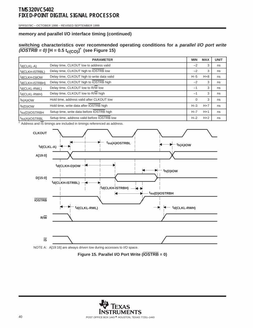
TMS320VC5402FIXED-POINT DIGITAL SIGNAL PROCESSOR
SPRS079C – OCTOBER 1998 – REVISED SEPTEMBER 1999
40 POST OFFICE BOX 1443 • HOUSTON, TEXAS 77251–1443
memory and parallel I/O interface timing (continued)
switching characteristics over recommended operating conditions for a parallel I/O port write(IOSTRB = 0) [H = 0.5 tc(CO)]† (see Figure 15)
PARAMETER MIN MAX UNIT
td(CLKL-A) Delay time, CLKOUT low to address valid –2 3 ns
td(CLKH-ISTRBL) Delay time, CLKOUT high to IOSTRB low –2 3 ns
td(CLKH-D)IOW Delay time, CLKOUT high to write data valid H–5 H+8 ns
td(CLKH-ISTRBH) Delay time, CLKOUT high to IOSTRB high –2 3 ns
td(CLKL-RWL) Delay time, CLKOUT low to R/W low –1 3 ns
td(CLKL-RWH) Delay time, CLKOUT low to R/W high –1 3 ns
th(A)IOW Hold time, address valid after CLKOUT low 0 3 ns
th(D)IOW Hold time, write data after IOSTRB high H–3 H+7 ns
tsu(D)IOSTRBH Setup time, write data before IOSTRB high H–7 H+1 ns
tsu(A)IOSTRBL Setup time, address valid before IOSTRB low H–2 H+2 ns
† Address and IS timings are included in timings referenced as address.
IS
R/W
IOSTRB
D[15:0]
A[19:0]
CLKOUT
td(CLKH-ISTRBH)
th(A)IOW
th(D)IOW
td(CLKH-D)IOW
td(CLKH-ISTRBL)
td(CLKL-A)
td(CLKL-RWL) td(CLKL-RWH)
tsu(A)IOSTRBL
tsu(D)IOSTRBH
NOTE A: A[19:16] are always driven low during accesses to I/O space.
Figure 15. Parallel I/O Port Write (IOSTRB = 0)
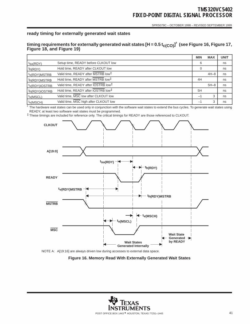
TMS320VC5402FIXED-POINT DIGITAL SIGNAL PROCESSOR
SPRS079C – OCTOBER 1998 – REVISED SEPTEMBER 1999
41POST OFFICE BOX 1443 • HOUSTON, TEXAS 77251–1443
ready timing for externally generated wait states
timing requirements for externally generated wait states [H = 0.5 t c(CO)]† (see Figure 16, Figure 17,Figure 18, and Figure 19)
MIN MAX UNIT
tsu(RDY) Setup time, READY before CLKOUT low 6 ns
th(RDY) Hold time, READY after CLKOUT low 0 ns
tv(RDY)MSTRB Valid time, READY after MSTRB low‡ 4H–8 ns
th(RDY)MSTRB Hold time, READY after MSTRB low‡ 4H ns
tv(RDY)IOSTRB Valid time, READY after IOSTRB low‡ 5H–8 ns
th(RDY)IOSTRB Hold time, READY after IOSTRB low‡ 5H ns
tv(MSCL) Valid time, MSC low after CLKOUT low –1 3 ns
tv(MSCH) Valid time, MSC high after CLKOUT low –1 3 ns
† The hardware wait states can be used only in conjunction with the software wait states to extend the bus cycles. To generate wait states usingREADY, at least two software wait states must be programmed.
‡ These timings are included for reference only. The critical timings for READY are those referenced to CLKOUT.
MSC
MSTRB
READY
A[19:0]
CLKOUT
tv(MSCH)tv(MSCL)
th(RDY)
th(RDY)MSTRB
tv(RDY)MSTRB
Wait State Generatedby READYWait States
Generated Internally
tsu(RDY)
NOTE A: A[19:16] are always driven low during accesses to external data space.
Figure 16. Memory Read With Externally Generated Wait States
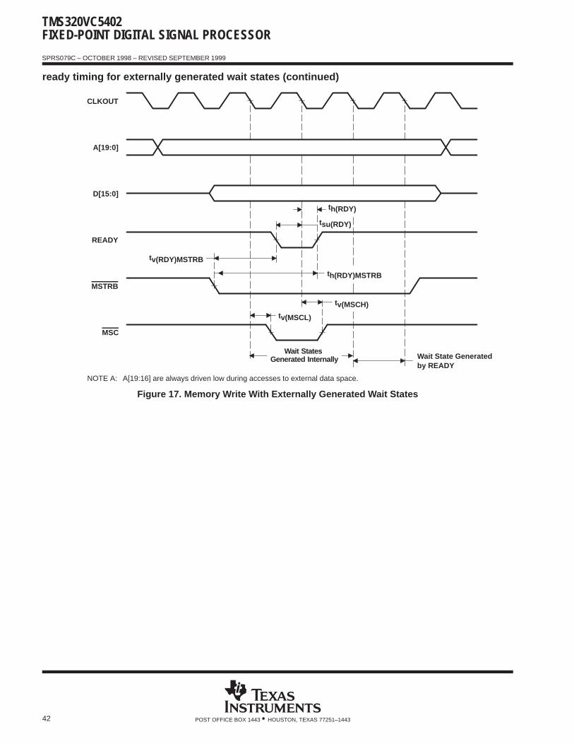
TMS320VC5402FIXED-POINT DIGITAL SIGNAL PROCESSOR
SPRS079C – OCTOBER 1998 – REVISED SEPTEMBER 1999
42 POST OFFICE BOX 1443 • HOUSTON, TEXAS 77251–1443
ready timing for externally generated wait states (continued)
MSC
MSTRB
READY
D[15:0]
A[19:0]
CLKOUT
tv(MSCH)
th(RDY)
Wait State Generatedby READY
Wait States Generated Internally
th(RDY)MSTRB
tv(RDY)MSTRB
tv(MSCL)
tsu(RDY)
NOTE A: A[19:16] are always driven low during accesses to external data space.
Figure 17. Memory Write With Externally Generated Wait States
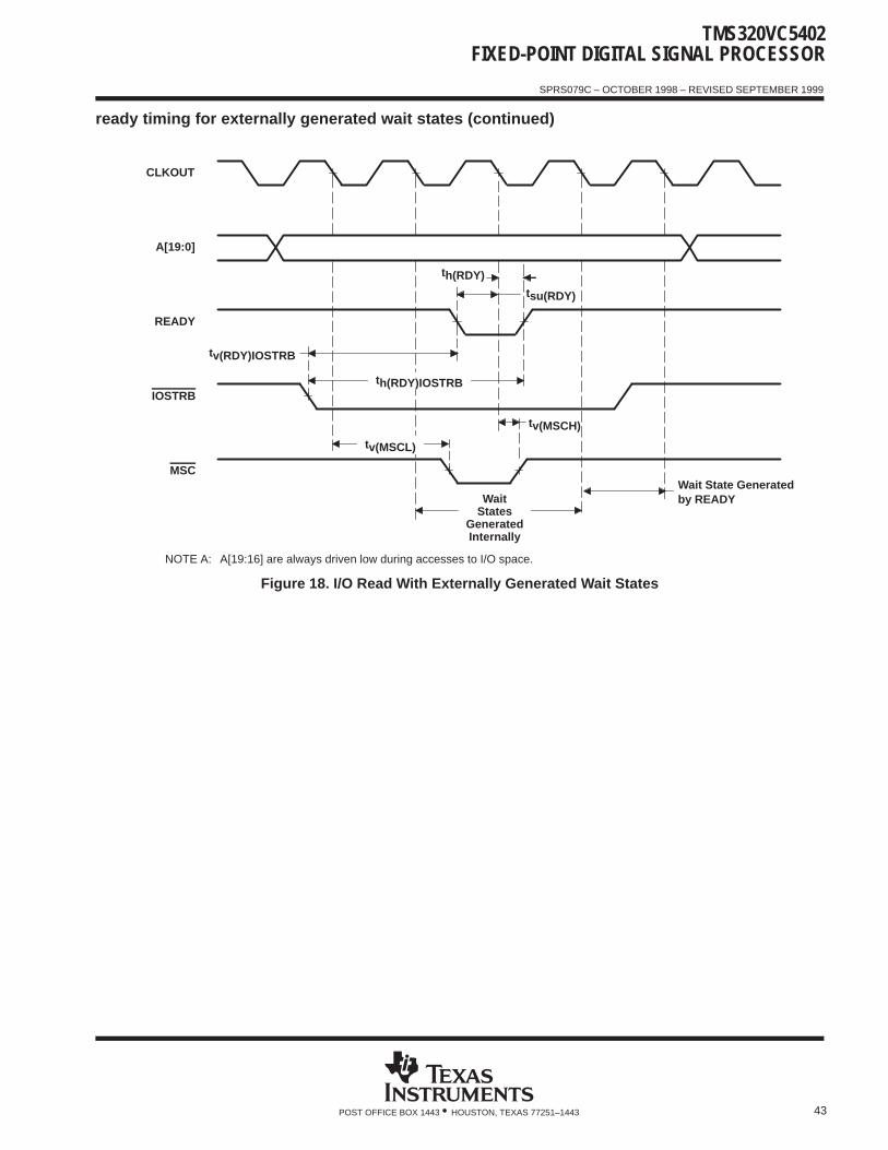
TMS320VC5402FIXED-POINT DIGITAL SIGNAL PROCESSOR
SPRS079C – OCTOBER 1998 – REVISED SEPTEMBER 1999
43POST OFFICE BOX 1443 • HOUSTON, TEXAS 77251–1443
ready timing for externally generated wait states (continued)
tsu(RDY)
MSC
IOSTRB
READY
A[19:0]
CLKOUT
tv(MSCH)
th(RDY)
Wait State Generatedby READYWait
StatesGeneratedInternally
tv(RDY)IOSTRB
tv(MSCL)
th(RDY)IOSTRB
NOTE A: A[19:16] are always driven low during accesses to I/O space.
Figure 18. I/O Read With Externally Generated Wait States
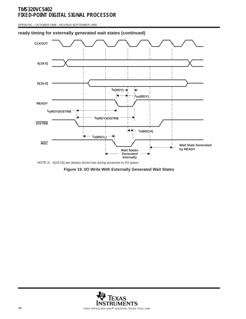
TMS320VC5402FIXED-POINT DIGITAL SIGNAL PROCESSOR
SPRS079C – OCTOBER 1998 – REVISED SEPTEMBER 1999
44 POST OFFICE BOX 1443 • HOUSTON, TEXAS 77251–1443
ready timing for externally generated wait states (continued)
IOSTRB
MSC
READY
D[15:0]
A[19:0]
CLKOUT
th(RDY)
Wait State Generatedby READYWait States
GeneratedInternally
tv(RDY)IOSTRB
tsu(RDY)
tv(MSCH)
tv(MSCL)
th(RDY)IOSTRB
NOTE A: A[19:16] are always driven low during accesses to I/O space.
Figure 19. I/O Write With Externally Generated Wait States
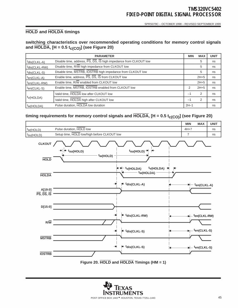
TMS320VC5402FIXED-POINT DIGITAL SIGNAL PROCESSOR
SPRS079C – OCTOBER 1998 – REVISED SEPTEMBER 1999
45POST OFFICE BOX 1443 • HOUSTON, TEXAS 77251–1443
HOLD and HOLDA timings
switching characteristics over recommended operating conditions for memory control signalsand HOLDA , [H = 0.5 tc(CO)] (see Figure 20)
PARAMETER MIN MAX UNIT
tdis(CLKL-A) Disable time, address, PS, DS, IS high impedance from CLKOUT low 5 ns
tdis(CLKL-RW) Disable time, R/W high impedance from CLKOUT low 5 ns
tdis(CLKL-S) Disable time, MSTRB, IOSTRB high impedance from CLKOUT low 5 ns
ten(CLKL-A) Enable time, address, PS, DS, IS from CLKOUT low 2H+5 ns
ten(CLKL-RW) Enable time, R/W enabled from CLKOUT low 2H+5 ns
ten(CLKL-S) Enable time, MSTRB, IOSTRB enabled from CLKOUT low 2 2H+5 ns
t (HOLDA)Valid time, HOLDA low after CLKOUT low –1 2 ns
tv(HOLDA)Valid time, HOLDA high after CLKOUT low –1 2 ns
tw(HOLDA) Pulse duration, HOLDA low duration 2H–1 ns
timing requirements for memory control signals and HOLDA , [H = 0.5 tc(CO)] (see Figure 20)
MIN MAX UNIT
tw(HOLD) Pulse duration, HOLD low 4H+7 ns
tsu(HOLD) Setup time, HOLD low/high before CLKOUT low 7 ns
IOSTRB
MSTRB
R/W
D[15:0]
PS, DS, ISA[19:0]
HOLDA
HOLD
CLKOUT
ten(CLKL-S)
ten(CLKL-S)
ten(CLKL-RW)
tdis(CLKL-S)
tdis(CLKL-S)
tdis(CLKL-RW)
tdis(CLKL-A)
tv(HOLDA) tv(HOLDA)tw(HOLDA)
tw(HOLD)
tsu(HOLD) tsu(HOLD)
ten(CLKL-A)
Figure 20. HOLD and HOLDA Timings (HM = 1)
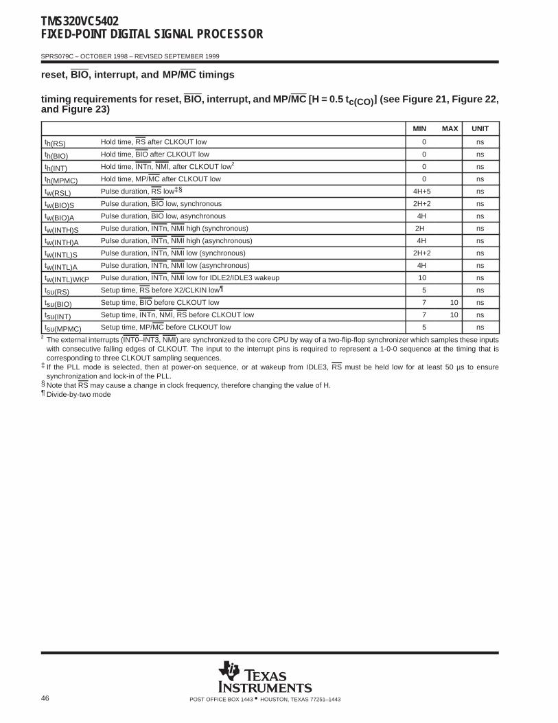
TMS320VC5402FIXED-POINT DIGITAL SIGNAL PROCESSOR
SPRS079C – OCTOBER 1998 – REVISED SEPTEMBER 1999
46 POST OFFICE BOX 1443 • HOUSTON, TEXAS 77251–1443
reset, BIO , interrupt, and MP/MC timings
timing requirements for reset, BIO , interrupt, and MP/MC [H = 0.5 tc(CO)] (see Figure 21, Figure 22,and Figure 23)
MIN MAX UNITMIN MAX UNIT
th(RS) Hold time, RS after CLKOUT low 0 ns
th(BIO) Hold time, BIO after CLKOUT low 0 ns
th(INT) Hold time, INTn, NMI, after CLKOUT low† 0 ns
th(MPMC) Hold time, MP/MC after CLKOUT low 0 ns
tw(RSL) Pulse duration, RS lowठ4H+5 ns
tw(BIO)S Pulse duration, BIO low, synchronous 2H+2 ns
tw(BIO)A Pulse duration, BIO low, asynchronous 4H ns
tw(INTH)S Pulse duration, INTn, NMI high (synchronous) 2H ns
tw(INTH)A Pulse duration, INTn, NMI high (asynchronous) 4H ns
tw(INTL)S Pulse duration, INTn, NMI low (synchronous) 2H+2 ns
tw(INTL)A Pulse duration, INTn, NMI low (asynchronous) 4H ns
tw(INTL)WKP Pulse duration, INTn, NMI low for IDLE2/IDLE3 wakeup 10 ns
tsu(RS) Setup time, RS before X2/CLKIN low¶ 5 ns
tsu(BIO) Setup time, BIO before CLKOUT low 7 10 ns
tsu(INT) Setup time, INTn, NMI, RS before CLKOUT low 7 10 ns
tsu(MPMC) Setup time, MP/MC before CLKOUT low 5 ns
† The external interrupts (INT0–INT3, NMI) are synchronized to the core CPU by way of a two-flip-flop synchronizer which samples these inputswith consecutive falling edges of CLKOUT. The input to the interrupt pins is required to represent a 1-0-0 sequence at the timing that iscorresponding to three CLKOUT sampling sequences.
‡ If the PLL mode is selected, then at power-on sequence, or at wakeup from IDLE3, RS must be held low for at least 50 µs to ensuresynchronization and lock-in of the PLL.
§ Note that RS may cause a change in clock frequency, therefore changing the value of H.¶ Divide-by-two mode
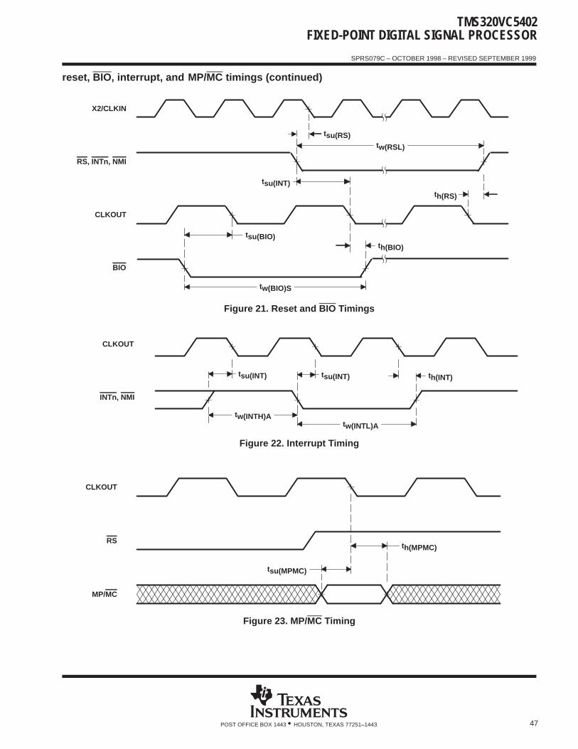
TMS320VC5402FIXED-POINT DIGITAL SIGNAL PROCESSOR
SPRS079C – OCTOBER 1998 – REVISED SEPTEMBER 1999
47POST OFFICE BOX 1443 • HOUSTON, TEXAS 77251–1443
reset, BIO , interrupt, and MP/MC timings (continued)
BIO
CLKOUT
RS, INTn, NMI
X2/CLKIN
th(BIO)
th(RS)
tsu(INT)
tw(BIO)S
tsu(BIO)
tw(RSL)
tsu(RS)
Figure 21. Reset and BIO Timings
INTn, NMI
CLKOUT
th(INT)tsu(INT)tsu(INT)
tw(INTL)A
tw(INTH)A
Figure 22. Interrupt Timing
MP/MC
RS
CLKOUT
tsu(MPMC)
th(MPMC)
Figure 23. MP/MC Timing
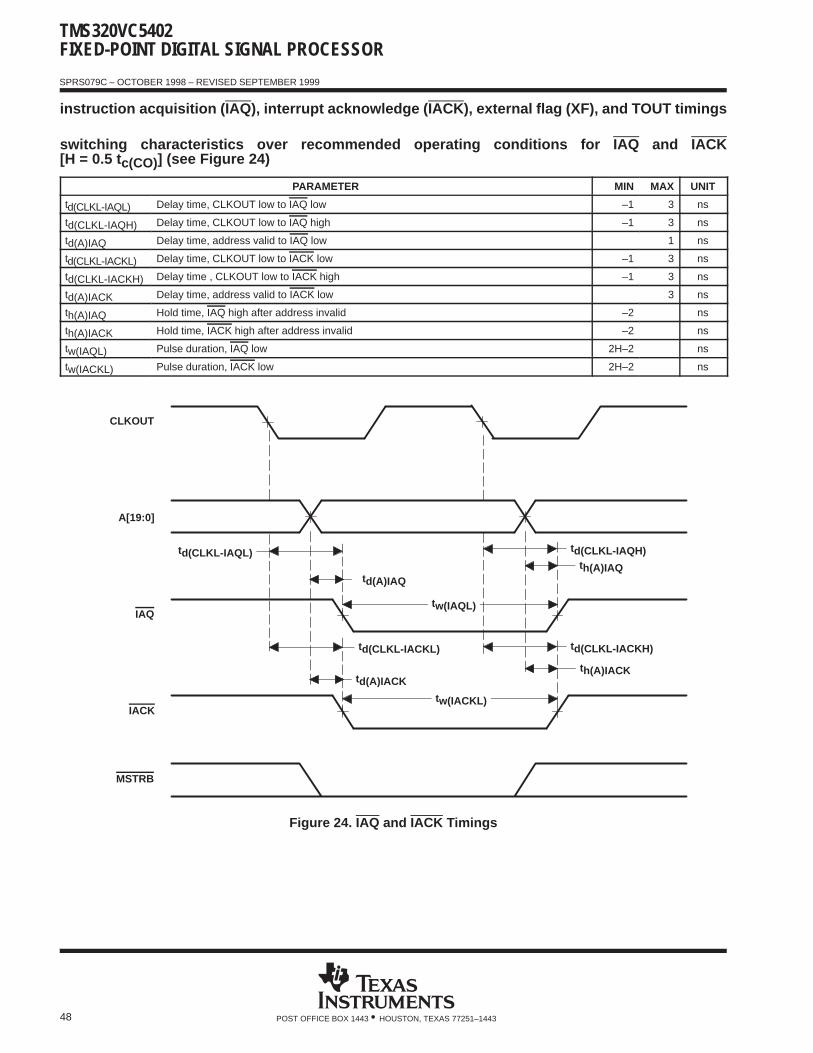
TMS320VC5402FIXED-POINT DIGITAL SIGNAL PROCESSOR
SPRS079C – OCTOBER 1998 – REVISED SEPTEMBER 1999
48 POST OFFICE BOX 1443 • HOUSTON, TEXAS 77251–1443
instruction acquisition (IAQ ), interrupt acknowledge (IACK ), external flag (XF), and TOUT timings
switching characteristics over recommended operating conditions for IAQ and IACK[H = 0.5 tc(CO)] (see Figure 24)
PARAMETER MIN MAX UNIT
td(CLKL-IAQL) Delay time, CLKOUT low to IAQ low –1 3 ns
td(CLKL-IAQH) Delay time, CLKOUT low to IAQ high –1 3 ns
td(A)IAQ Delay time, address valid to IAQ low 1 ns
td(CLKL-IACKL) Delay time, CLKOUT low to IACK low –1 3 ns
td(CLKL-IACKH) Delay time , CLKOUT low to IACK high –1 3 ns
td(A)IACK Delay time, address valid to IACK low 3 ns
th(A)IAQ Hold time, IAQ high after address invalid –2 ns
th(A)IACK Hold time, IACK high after address invalid –2 ns
tw(IAQL) Pulse duration, IAQ low 2H–2 ns
tw(IACKL) Pulse duration, IACK low 2H–2 ns
MSTRB
IACK
IAQ
A[19:0]
CLKOUT
td(A)IACK
td(A)IAQ
tw(IACKL)
th(A)IACK
td(CLKL-IACKL)
tw(IAQL)
th(A)IAQ
td(CLKL-IAQL)
td(CLKL-IACKH)
td(CLKL-IAQH)
Figure 24. IAQ and IACK Timings
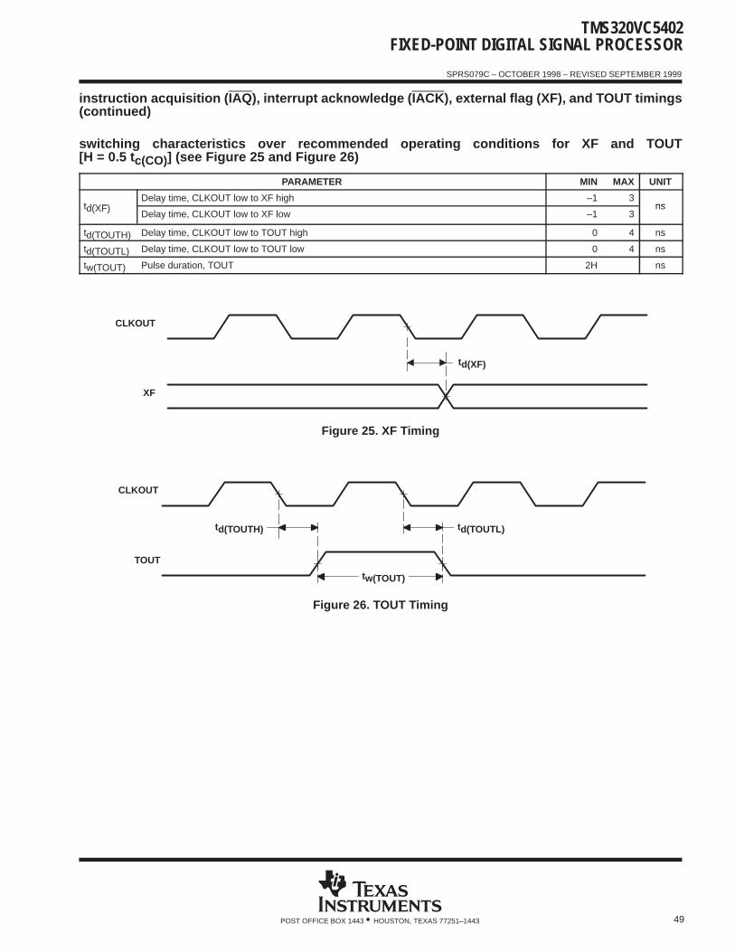
TMS320VC5402FIXED-POINT DIGITAL SIGNAL PROCESSOR
SPRS079C – OCTOBER 1998 – REVISED SEPTEMBER 1999
49POST OFFICE BOX 1443 • HOUSTON, TEXAS 77251–1443
instruction acquisition (IAQ ), interrupt acknowledge (IACK ), external flag (XF), and TOUT timings(continued)
switching characteristics over recommended operating conditions for XF and TOUT[H = 0.5 tc(CO)] (see Figure 25 and Figure 26)
PARAMETER MIN MAX UNIT
td(XF)Delay time, CLKOUT low to XF high –1 3
nstd(XF)Delay time, CLKOUT low to XF low –1 3
ns
td(TOUTH) Delay time, CLKOUT low to TOUT high 0 4 ns
td(TOUTL) Delay time, CLKOUT low to TOUT low 0 4 ns
tw(TOUT) Pulse duration, TOUT 2H ns
XF
CLKOUT
td(XF)
Figure 25. XF Timing
TOUT
CLKOUT
tw(TOUT)
td(TOUTL)td(TOUTH)
Figure 26. TOUT Timing
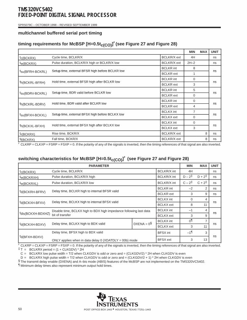
TMS320VC5402FIXED-POINT DIGITAL SIGNAL PROCESSOR
SPRS079C – OCTOBER 1998 – REVISED SEPTEMBER 1999
50 POST OFFICE BOX 1443 • HOUSTON, TEXAS 77251–1443
multichannel buffered serial port timing
timing requirements for McBSP [H=0.5t c(CO)]†(see Figure 27 and Figure 28)
MIN MAX UNIT
tc(BCKRX) Cycle time, BCLKR/X BCLKR/X ext 4H ns
tw(BCKRX) Pulse duration, BCLKR/X high or BCLKR/X low BCLKR/X ext 2H–2 ns
t (BFRH BCKRL) Setup time external BFSR high before BCLKR lowBCLKR int 8
nstsu(BFRH-BCKRL) Setup time, external BFSR high before BCLKR lowBCLKR ext 1
ns
th(BCKRL BFRH) Hold time external BFSR high after BCLKR lowBCLKR int 0
nsth(BCKRL-BFRH) Hold time, external BFSR high after BCLKR lowBCLKR ext 3
ns
t (BDRV BCKRL) Setup time BDR valid before BCLKR lowBCLKR int 5
nstsu(BDRV-BCKRL) Setup time, BDR valid before BCLKR lowBCLKR ext 0
ns
th(BCKRL BDRV) Hold time BDR valid after BCLKR lowBCLKR int 0
nsth(BCKRL-BDRV) Hold time, BDR valid after BCLKR lowBCLKR ext 4
ns
t (BFXH BCKXL) Setup time external BFSX high before BCLKX lowBCLKX int 7
nstsu(BFXH-BCKXL) Setup time, external BFSX high before BCLKX lowBCLKX ext 0
ns
th(BCKXL BFXH) Hold time external BFSX high after BCLKX lowBCLKX int 0
nsth(BCKXL-BFXH) Hold time, external BFSX high after BCLKX lowBCLKX ext 3
ns
tr(BCKRX) Rise time, BCKR/X BCLKR/X ext 8 ns
tf(BCKRX) Fall time, BCKR/X BCLKR/X ext 8 ns
† CLKRP = CLKXP = FSRP = FSXP = 0. If the polarity of any of the signals is inverted, then the timing references of that signal are also inverted.
switching characteristics for McBSP [H=0.5t c(CO)]† (see Figure 27 and Figure 28)
PARAMETER MIN MAX UNIT
tc(BCKRX) Cycle time, BCLKR/X BCLKR/X int 4H ns
tw(BCKRXH) Pulse duration, BCLKR/X high BCLKR/X int D – 2‡ D + 2‡ ns
tw(BCKRXL) Pulse duration, BCLKR/X low BCLKR/X int C – 2‡ C + 2‡ ns
td(BCKRH BFRV) Delay time BCLKR high to internal BFSR validBCLKR int –2 2 ns
td(BCKRH-BFRV) Delay time, BCLKR high to internal BFSR validBCLKR ext 3 9 ns
td(BCKXH BFXV) Delay time BCLKX high to internal BFSX validBCLKX int 0 4
nstd(BCKXH-BFXV) Delay time, BCLKX high to internal BFSX validBCLKX ext 8 11
ns
tdi (BCKXH BDXHZ)Disable time, BCLKX high to BDX high impedance following last data BCLKX int –1 4
nstdis(BCKXH-BDXHZ), g g g
bit of transfer BCLKX ext 3 9ns
td(BCKXH BDXV) Delay time BCLKX high to BDX valid DXENA 0§BCLKX int 0¶ 7
nstd(BCKXH-BDXV) Delay time, BCLKX high to BDX valid DXENA = 0§BCLKX ext 3 11
ns
td(BFXH BDXV)
Delay time, BFSX high to BDX valid BFSX int –1¶ 3nstd(BFXH-BDXV)
ONLY applies when in data delay 0 (XDATDLY = 00b) mode BFSX ext 3 13ns
† CLKRP = CLKXP = FSRP = FSXP = 0. If the polarity of any of the signals is inverted, then the timing references of that signal are also inverted.‡ T = BCLKRX period = (1 + CLKGDV) * 2H
C = BCLKRX low pulse width = T/2 when CLKGDV is odd or zero and = (CLKGDV/2) * 2H when CLKGDV is evenD = BCLKRX high pulse width = T/2 when CLKGDV is odd or zero and = (CLKGDV/2 + 1) * 2H when CLKGDV is even
§ The transmit delay enable (DXENA) and A–bis mode (ABIS) features of the McBSP are not implemented on the TMS320VC5402.¶ Minimum delay times also represent minimum output hold times.
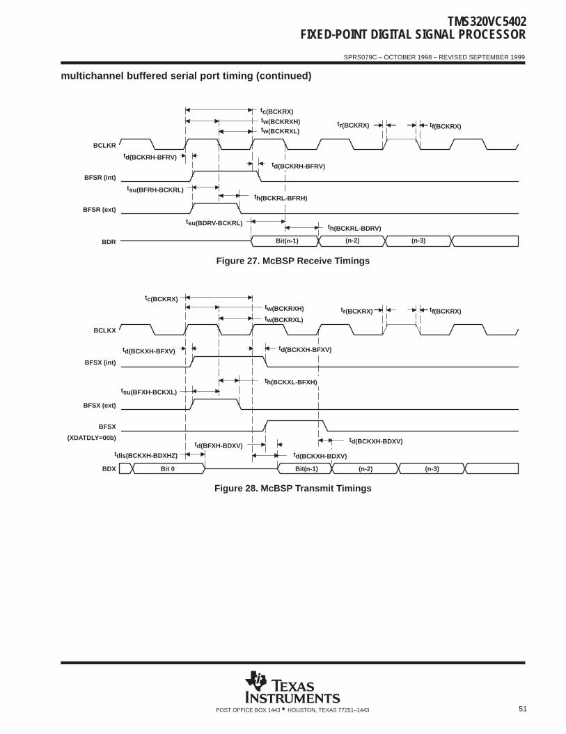
TMS320VC5402FIXED-POINT DIGITAL SIGNAL PROCESSOR
SPRS079C – OCTOBER 1998 – REVISED SEPTEMBER 1999
51POST OFFICE BOX 1443 • HOUSTON, TEXAS 77251–1443
multichannel buffered serial port timing (continued)
Bit(n-1) (n-2) (n-3)
BCLKR
BFSR (int)
BFSR (ext)
BDR
tw(BCKRXH)
tc(BCKRX)
tw(BCKRXL)
td(BCKRH-BFRV)td(BCKRH-BFRV)
tsu(BFRH-BCKRL)th(BCKRL-BFRH)
th(BCKRL-BDRV)tsu(BDRV-BCKRL)
tr(BCKRX) tf(BCKRX)
Figure 27. McBSP Receive Timings
Bit 0 Bit(n-1) (n-2) (n-3)
BCLKX
BFSX (int)
BFSX (ext)
BFSX
BDX
tc(BCKRX)tw(BCKRXH)tw(BCKRXL)
td(BCKXH-BFXV)
tsu(BFXH-BCKXL)
th(BCKXL-BFXH)
tdis(BCKXH-BDXHZ)
td(BFXH-BDXV)td(BCKXH-BDXV)
td(BCKXH-BDXV)
(XDATDLY=00b)
tr(BCKRX) tf(BCKRX)
td(BCKXH-BFXV)
Figure 28. McBSP Transmit Timings
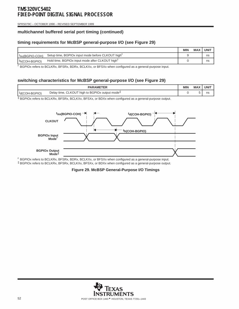
TMS320VC5402FIXED-POINT DIGITAL SIGNAL PROCESSOR
SPRS079C – OCTOBER 1998 – REVISED SEPTEMBER 1999
52 POST OFFICE BOX 1443 • HOUSTON, TEXAS 77251–1443
multichannel buffered serial port timing (continued)
timing requirements for McBSP general-purpose I/O (see Figure 29)
MIN MAX UNIT
tsu(BGPIO-COH) Setup time, BGPIOx input mode before CLKOUT high† 9 ns
th(COH-BGPIO) Hold time, BGPIOx input mode after CLKOUT high† 0 ns
† BGPIOx refers to BCLKRx, BFSRx, BDRx, BCLKXx, or BFSXx when configured as a general-purpose input.
switching characteristics for McBSP general-purpose I/O (see Figure 29)
PARAMETER MIN MAX UNIT
td(COH-BGPIO) Delay time, CLKOUT high to BGPIOx output mode‡ 0 5 ns
‡ BGPIOx refers to BCLKRx, BFSRx, BCLKXx, BFSXx, or BDXx when configured as a general-purpose output.
tsu(BGPIO-COH)
th(COH-BGPIO)
td(COH-BGPIO)
CLKOUT
BGPIOx InputMode†
BGPIOx OutputMode‡
† BGPIOx refers to BCLKRx, BFSRx, BDRx, BCLKXx, or BFSXx when configured as a general-purpose input.‡ BGPIOx refers to BCLKRx, BFSRx, BCLKXx, BFSXx, or BDXx when configured as a general-purpose output.
Figure 29. McBSP General-Purpose I/O Timings
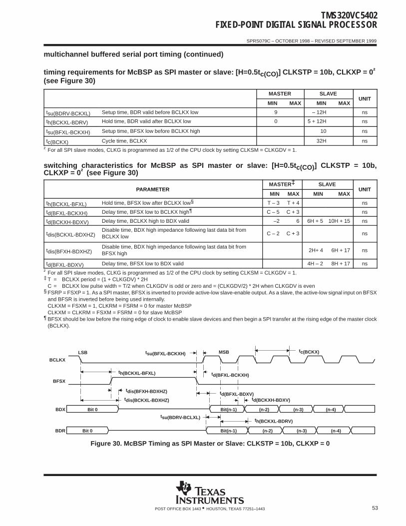
TMS320VC5402FIXED-POINT DIGITAL SIGNAL PROCESSOR
SPRS079C – OCTOBER 1998 – REVISED SEPTEMBER 1999
53POST OFFICE BOX 1443 • HOUSTON, TEXAS 77251–1443
multichannel buffered serial port timing (continued)
timing requirements for McBSP as SPI master or slave: [H=0.5t c(CO)] CLKSTP = 10b, CLKXP = 0 †
(see Figure 30)
MASTER SLAVEUNIT
MIN MAX MIN MAXUNIT
tsu(BDRV-BCKXL) Setup time, BDR valid before BCLKX low 9 – 12H ns
th(BCKXL-BDRV) Hold time, BDR valid after BCLKX low 0 5 + 12H ns
tsu(BFXL-BCKXH) Setup time, BFSX low before BCLKX high 10 ns
tc(BCKX) Cycle time, BCLKX 32H ns
† For all SPI slave modes, CLKG is programmed as 1/2 of the CPU clock by setting CLKSM = CLKGDV = 1.
switching characteristics for McBSP as SPI master or slave: [H=0.5t c(CO)] CLKSTP = 10b,CLKXP = 0† (see Figure 30)
PARAMETERMASTER‡ SLAVE
UNITPARAMETERMIN MAX MIN MAX
UNIT
th(BCKXL-BFXL) Hold time, BFSX low after BCLKX low§ T – 3 T + 4 ns
td(BFXL-BCKXH) Delay time, BFSX low to BCLKX high¶ C – 5 C + 3 ns
td(BCKXH-BDXV) Delay time, BCLKX high to BDX valid –2 6 6H + 5 10H + 15 ns
tdis(BCKXL-BDXHZ)Disable time, BDX high impedance following last data bit fromBCLKX low
C – 2 C + 3 ns
tdis(BFXH-BDXHZ)Disable time, BDX high impedance following last data bit fromBFSX high
2H+ 4 6H + 17 ns
td(BFXL-BDXV) Delay time, BFSX low to BDX valid 4H – 2 8H + 17 ns
† For all SPI slave modes, CLKG is programmed as 1/2 of the CPU clock by setting CLKSM = CLKGDV = 1.‡ T = BCLKX period = (1 + CLKGDV) * 2H
C = BCLKX low pulse width = T/2 when CLKGDV is odd or zero and = (CLKGDV/2) * 2H when CLKGDV is even§ FSRP = FSXP = 1. As a SPI master, BFSX is inverted to provide active-low slave-enable output. As a slave, the active-low signal input on BFSX
and BFSR is inverted before being used internally.CLKXM = FSXM = 1, CLKRM = FSRM = 0 for master McBSPCLKXM = CLKRM = FSXM = FSRM = 0 for slave McBSP
¶ BFSX should be low before the rising edge of clock to enable slave devices and then begin a SPI transfer at the rising edge of the master clock(BCLKX).
Bit 0 Bit(n-1) (n-2) (n-3) (n-4)
Bit 0 Bit(n-1) (n-2) (n-3) (n-4)
BCLKX
BFSX
BDX
BDR
tsu(BDRV-BCLXL)
td(BCKXH-BDXV)
th(BCKXL-BDRV)
tdis(BFXH-BDXHZ)
tdis(BCKXL-BDXHZ)
th(BCKXL-BFXL)
td(BFXL-BDXV)
td(BFXL-BCKXH)
LSB MSBtsu(BFXL-BCKXH)tc(BCKX)
Figure 30. McBSP Timing as SPI Master or Slave: CLKSTP = 10b, CLKXP = 0
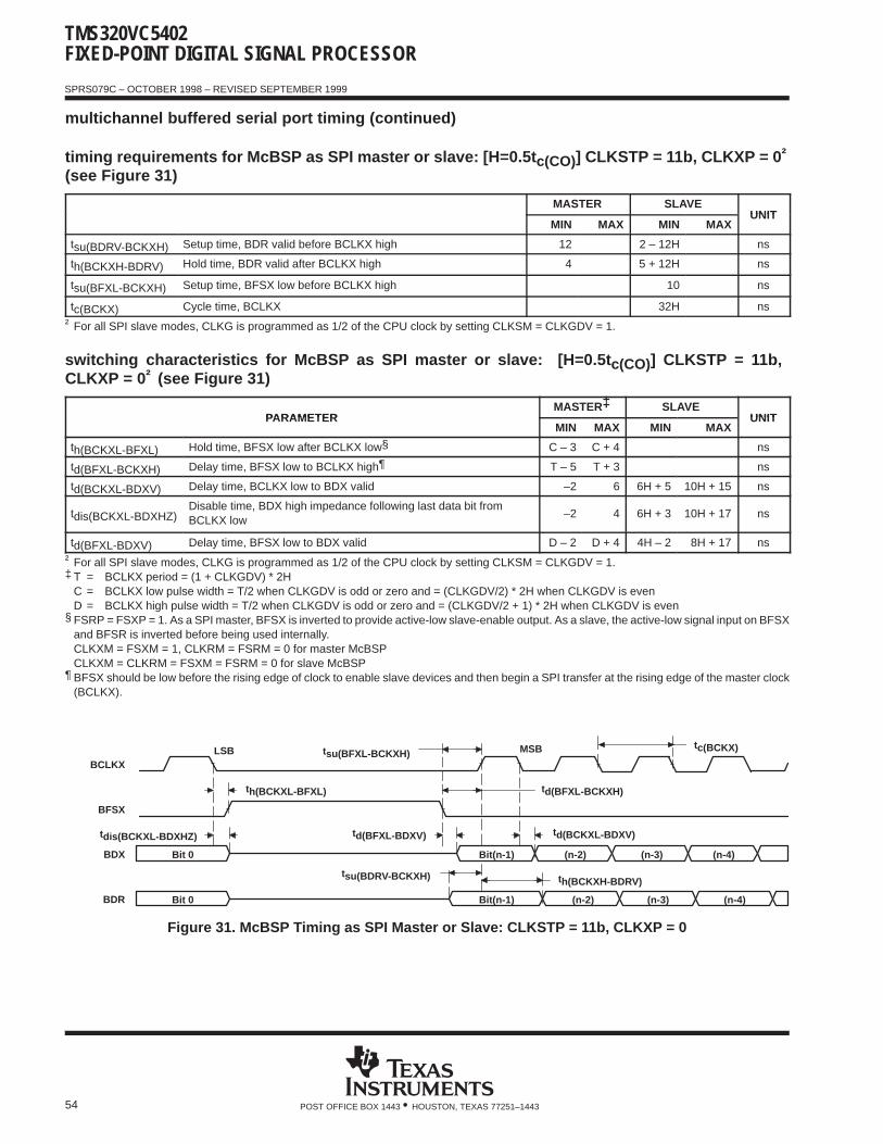
TMS320VC5402FIXED-POINT DIGITAL SIGNAL PROCESSOR
SPRS079C – OCTOBER 1998 – REVISED SEPTEMBER 1999
54 POST OFFICE BOX 1443 • HOUSTON, TEXAS 77251–1443
multichannel buffered serial port timing (continued)
timing requirements for McBSP as SPI master or slave: [H=0.5t c(CO)] CLKSTP = 11b, CLKXP = 0 †
(see Figure 31)
MASTER SLAVEUNIT
MIN MAX MIN MAXUNIT
tsu(BDRV-BCKXH) Setup time, BDR valid before BCLKX high 12 2 – 12H ns
th(BCKXH-BDRV) Hold time, BDR valid after BCLKX high 4 5 + 12H ns
tsu(BFXL-BCKXH) Setup time, BFSX low before BCLKX high 10 ns
tc(BCKX) Cycle time, BCLKX 32H ns
† For all SPI slave modes, CLKG is programmed as 1/2 of the CPU clock by setting CLKSM = CLKGDV = 1.
switching characteristics for McBSP as SPI master or slave: [H=0.5t c(CO)] CLKSTP = 11b, CLKXP = 0† (see Figure 31)
PARAMETERMASTER‡ SLAVE
UNITPARAMETERMIN MAX MIN MAX
UNIT
th(BCKXL-BFXL) Hold time, BFSX low after BCLKX low§ C – 3 C + 4 ns
td(BFXL-BCKXH) Delay time, BFSX low to BCLKX high¶ T – 5 T + 3 ns
td(BCKXL-BDXV) Delay time, BCLKX low to BDX valid –2 6 6H + 5 10H + 15 ns
tdis(BCKXL-BDXHZ)Disable time, BDX high impedance following last data bit fromBCLKX low
–2 4 6H + 3 10H + 17 ns
td(BFXL-BDXV) Delay time, BFSX low to BDX valid D – 2 D + 4 4H – 2 8H + 17 ns
† For all SPI slave modes, CLKG is programmed as 1/2 of the CPU clock by setting CLKSM = CLKGDV = 1.‡ T = BCLKX period = (1 + CLKGDV) * 2H
C = BCLKX low pulse width = T/2 when CLKGDV is odd or zero and = (CLKGDV/2) * 2H when CLKGDV is evenD = BCLKX high pulse width = T/2 when CLKGDV is odd or zero and = (CLKGDV/2 + 1) * 2H when CLKGDV is even
§ FSRP = FSXP = 1. As a SPI master, BFSX is inverted to provide active-low slave-enable output. As a slave, the active-low signal input on BFSXand BFSR is inverted before being used internally.CLKXM = FSXM = 1, CLKRM = FSRM = 0 for master McBSPCLKXM = CLKRM = FSXM = FSRM = 0 for slave McBSP
¶ BFSX should be low before the rising edge of clock to enable slave devices and then begin a SPI transfer at the rising edge of the master clock(BCLKX).
Bit 0 Bit(n-1) (n-2) (n-3) (n-4)
Bit 0 Bit(n-1) (n-2) (n-3) (n-4)
BCLKX
BFSX
BDX
BDR
td(BFXL-BCKXH)
tdis(BCKXL-BDXHZ) td(BCKXL-BDXV)
th(BCKXH-BDRV)tsu(BDRV-BCKXH)
td(BFXL-BDXV)
th(BCKXL-BFXL)
LSB MSBtsu(BFXL-BCKXH)tc(BCKX)
Figure 31. McBSP Timing as SPI Master or Slave: CLKSTP = 11b, CLKXP = 0
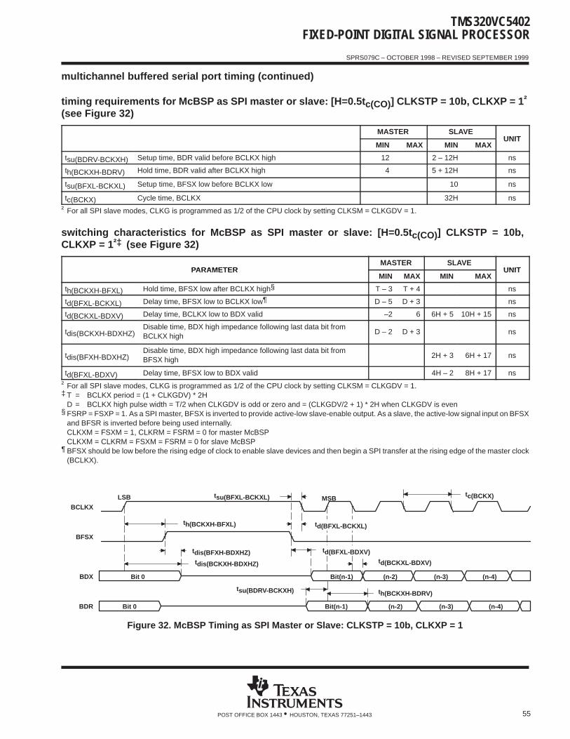
TMS320VC5402FIXED-POINT DIGITAL SIGNAL PROCESSOR
SPRS079C – OCTOBER 1998 – REVISED SEPTEMBER 1999
55POST OFFICE BOX 1443 • HOUSTON, TEXAS 77251–1443
multichannel buffered serial port timing (continued)
timing requirements for McBSP as SPI master or slave: [H=0.5t c(CO)] CLKSTP = 10b, CLKXP = 1 †
(see Figure 32)
MASTER SLAVEUNIT
MIN MAX MIN MAXUNIT
tsu(BDRV-BCKXH) Setup time, BDR valid before BCLKX high 12 2 – 12H ns
th(BCKXH-BDRV) Hold time, BDR valid after BCLKX high 4 5 + 12H ns
tsu(BFXL-BCKXL) Setup time, BFSX low before BCLKX low 10 ns
tc(BCKX) Cycle time, BCLKX 32H ns
† For all SPI slave modes, CLKG is programmed as 1/2 of the CPU clock by setting CLKSM = CLKGDV = 1.
switching characteristics for McBSP as SPI master or slave: [H=0.5t c(CO)] CLKSTP = 10b, CLKXP = 1†‡ (see Figure 32)
PARAMETERMASTER SLAVE
UNITPARAMETERMIN MAX MIN MAX
UNIT
th(BCKXH-BFXL) Hold time, BFSX low after BCLKX high§ T – 3 T + 4 ns
td(BFXL-BCKXL) Delay time, BFSX low to BCLKX low¶ D – 5 D + 3 ns
td(BCKXL-BDXV) Delay time, BCLKX low to BDX valid –2 6 6H + 5 10H + 15 ns
tdis(BCKXH-BDXHZ)Disable time, BDX high impedance following last data bit fromBCLKX high
D – 2 D + 3 ns
tdis(BFXH-BDXHZ)Disable time, BDX high impedance following last data bit fromBFSX high
2H + 3 6H + 17 ns
td(BFXL-BDXV) Delay time, BFSX low to BDX valid 4H – 2 8H + 17 ns
† For all SPI slave modes, CLKG is programmed as 1/2 of the CPU clock by setting CLKSM = CLKGDV = 1.‡ T = BCLKX period = (1 + CLKGDV) * 2H
D = BCLKX high pulse width = T/2 when CLKGDV is odd or zero and = (CLKGDV/2 + 1) * 2H when CLKGDV is even§ FSRP = FSXP = 1. As a SPI master, BFSX is inverted to provide active-low slave-enable output. As a slave, the active-low signal input on BFSX
and BFSR is inverted before being used internally.CLKXM = FSXM = 1, CLKRM = FSRM = 0 for master McBSPCLKXM = CLKRM = FSXM = FSRM = 0 for slave McBSP
¶ BFSX should be low before the rising edge of clock to enable slave devices and then begin a SPI transfer at the rising edge of the master clock(BCLKX).
tsu(BFXL-BCKXL)
th(BCKXH-BDRV)
tdis(BFXH-BDXHZ)tdis(BCKXH-BDXHZ)
Bit 0 Bit(n-1) (n-2) (n-3) (n-4)
Bit 0 Bit(n-1) (n-2) (n-3) (n-4)
BCLKX
BFSX
BDX
BDR
td(BFXL-BCKXL)
td(BFXL-BDXV)td(BCKXL-BDXV)
tsu(BDRV-BCKXH)
th(BCKXH-BFXL)
LSB MSBtc(BCKX)
Figure 32. McBSP Timing as SPI Master or Slave: CLKSTP = 10b, CLKXP = 1
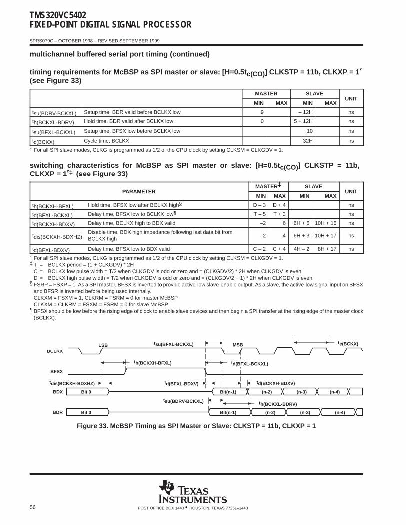
TMS320VC5402FIXED-POINT DIGITAL SIGNAL PROCESSOR
SPRS079C – OCTOBER 1998 – REVISED SEPTEMBER 1999
56 POST OFFICE BOX 1443 • HOUSTON, TEXAS 77251–1443
multichannel buffered serial port timing (continued)
timing requirements for McBSP as SPI master or slave: [H=0.5t c(CO)] CLKSTP = 11b, CLKXP = 1 †
(see Figure 33)
MASTER SLAVEUNIT
MIN MAX MIN MAXUNIT
tsu(BDRV-BCKXL) Setup time, BDR valid before BCLKX low 9 – 12H ns
th(BCKXL-BDRV) Hold time, BDR valid after BCLKX low 0 5 + 12H ns
tsu(BFXL-BCKXL) Setup time, BFSX low before BCLKX low 10 ns
tc(BCKX) Cycle time, BCLKX 32H ns
† For all SPI slave modes, CLKG is programmed as 1/2 of the CPU clock by setting CLKSM = CLKGDV = 1.
switching characteristics for McBSP as SPI master or slave: [H=0.5t c(CO)] CLKSTP = 11b, CLKXP = 1†‡ (see Figure 33)
PARAMETERMASTER‡ SLAVE
UNITPARAMETERMIN MAX MIN MAX
UNIT
th(BCKXH-BFXL) Hold time, BFSX low after BCLKX high§ D – 3 D + 4 ns
td(BFXL-BCKXL) Delay time, BFSX low to BCLKX low¶ T – 5 T + 3 ns
td(BCKXH-BDXV) Delay time, BCLKX high to BDX valid –2 6 6H + 5 10H + 15 ns
tdis(BCKXH-BDXHZ)Disable time, BDX high impedance following last data bit fromBCLKX high
–2 4 6H + 3 10H + 17 ns
td(BFXL-BDXV) Delay time, BFSX low to BDX valid C – 2 C + 4 4H – 2 8H + 17 ns
† For all SPI slave modes, CLKG is programmed as 1/2 of the CPU clock by setting CLKSM = CLKGDV = 1.‡ T = BCLKX period = (1 + CLKGDV) * 2H
C = BCLKX low pulse width = T/2 when CLKGDV is odd or zero and = (CLKGDV/2) * 2H when CLKGDV is evenD = BCLKX high pulse width = T/2 when CLKGDV is odd or zero and = (CLKGDV/2 + 1) * 2H when CLKGDV is even
§ FSRP = FSXP = 1. As a SPI master, BFSX is inverted to provide active-low slave-enable output. As a slave, the active-low signal input on BFSXand BFSR is inverted before being used internally.CLKXM = FSXM = 1, CLKRM = FSRM = 0 for master McBSPCLKXM = CLKRM = FSXM = FSRM = 0 for slave McBSP
¶ BFSX should be low before the rising edge of clock to enable slave devices and then begin a SPI transfer at the rising edge of the master clock(BCLKX).
Bit 0 Bit(n-1) (n-2) (n-3) (n-4)
Bit 0 Bit(n-1) (n-2) (n-3) (n-4)
BCLKX
BFSX
BDX
BDR
td(BFXL-BCKXL)
tsu(BDRV-BCKXL)
tdis(BCKXH-BDXHZ)
th(BCKXH-BFXL)
td(BCKXH-BDXV)
th(BCKXL-BDRV)
td(BFXL-BDXV)
LSB MSBtsu(BFXL-BCKXL) tc(BCKX)
Figure 33. McBSP Timing as SPI Master or Slave: CLKSTP = 11b, CLKXP = 1
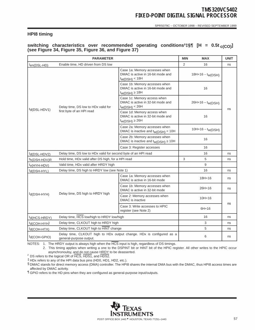
TMS320VC5402FIXED-POINT DIGITAL SIGNAL PROCESSOR
SPRS079C – OCTOBER 1998 – REVISED SEPTEMBER 1999
57POST OFFICE BOX 1443 • HOUSTON, TEXAS 77251–1443
HPI8 timing
switching characteristics over recommended operating conditions†‡§¶ [H = 0.5t c(CO)] (see Figure 34, Figure 35, Figure 36, and Figure 37)
PARAMETER MIN MAX UNIT
ten(DSL-HD) Enable time, HD driven from DS low 2 16 ns
Case 1a: Memory accesses whenDMAC is active in 16-bit mode andtw(DSH) < 18H
18H+16 – tw(DSH)
Case 1b: Memory accesses whenDMAC is active in 16-bit mode andtw(DSH) ≥ 18H
16
td(DSL HDV1)Delay time, DS low to HDx valid for
Case 1c: Memory access whenDMAC is active in 32-bit mode andtw(DSH) < 26H
26H+16 – tw(DSH)
nstd(DSL-HDV1)y
first byte of an HPI read Case 1d: Memory access whenDMAC is active in 32-bit mode andtw(DSH) ≥ 26H
16
ns
Case 2a: Memory accesses whenDMAC is inactive and tw(DSH) < 10H
10H+16 – tw(DSH)
Case 2b: Memory accesses whenDMAC is inactive and tw(DSH) ≥ 10H
16
Case 3: Register accesses 16
td(DSL-HDV2) Delay time, DS low to HDx valid for second byte of an HPI read 16 ns
th(DSH-HDV)R Hold time, HDx valid after DS high, for a HPI read 3 5 ns
tv(HYH-HDV) Valid time, HDx valid after HRDY high 9
td(DSH-HYL) Delay time, DS high to HRDY low (see Note 1) 16 ns
Case 1a: Memory accesses whenDMAC is active in 16-bit mode
18H+16 ns
t Delay time DS high to HRDY high
Case 1b: Memory accesses whenDMAC is active in 32-bit mode
26H+16 ns
td(DSH-HYH) Delay time, DS high to HRDY highCase 2: Memory accesses whenDMAC is inactive
10H+16
nsCase 3: Write accesses to HPICregister (see Note 2)
6H+16
ns
td(HCS-HRDY) Delay time, HCS low/high to HRDY low/high 16 ns
td(COH-HYH) Delay time, CLKOUT high to HRDY high 3 ns
td(COH-HTX) Delay time, CLKOUT high to HINT change 5 ns
td(COH-GPIO)Delay time, CLKOUT high to HDx output change. HDx is configured as ageneral-purpose output.
6 ns
NOTES: 1. The HRDY output is always high when the HCS input is high, regardless of DS timings.2. This timing applies when writing a one to the DSPINT bit or HINT bit of the HPIC register. All other writes to the HPIC occur
asynchronoulsy, and do not cause HRDY to be deasserted.† DS refers to the logical OR of HCS, HDS1, and HDS2.‡ HDx refers to any of the HPI data bus pins (HD0, HD1, HD2, etc.).§ DMAC stands for direct memory access (DMA) controller. The HPI8 shares the internal DMA bus with the DMAC, thus HPI8 access times are
affected by DMAC activity.¶ GPIO refers to the HD pins when they are configured as general-purpose input/outputs.

TMS320VC5402FIXED-POINT DIGITAL SIGNAL PROCESSOR
SPRS079C – OCTOBER 1998 – REVISED SEPTEMBER 1999
58 POST OFFICE BOX 1443 • HOUSTON, TEXAS 77251–1443
HPI8 timing (continued)
timing requirements†‡§ (see Figure 34, Figure 35, Figure 36, and Figure 37)
MIN MAX UNIT
tsu(HBV-DSL) Setup time, HBIL and HAD valid before DS low or before HAS low¶# 5 ns
th(DSL-HBV) Hold time, HBIL and HAD valid after DS low or after HAS low¶# 5 ns
tsu(HSL-DSL) Setup time, HAS low before DS low 10 ns
tw(DSL) Pulse duration, DS low 20 ns
tw(DSH) Pulse duration, DS high 10 ns
tsu(HDV-DSH) Setup time, HDx valid before DS high, HPI write 2 ns
th(DSH-HDV)W Hold time, HDx valid after DS high, HPI write 3 ns
tsu(GPIO-COH) Setup time, HDx input valid before CLKOUT high, HDx configured as general-purpose input 6 ns
th(GPIO-COH) Hold time, HDx input valid after CLKOUT high, HDx configured as general-purpose input 0 ns
† DS refers to the logical OR of HCS, HDS1, and HDS2.‡ HDx refers to any of the HPI data bus pins (HD0, HD1, HD2, etc.).§ GPIO refers to the HD pins when they are configured as general-purpose input/outputs.¶ HAD refers to HCNTL0, HCNTL1, and H/RW.# When the HAS signal is used to latch the control signals, this timing refers to the falling edge of the HAS signal. Otherwise, when HAS is not used
(always high), this timing refers to the falling edge of DS.
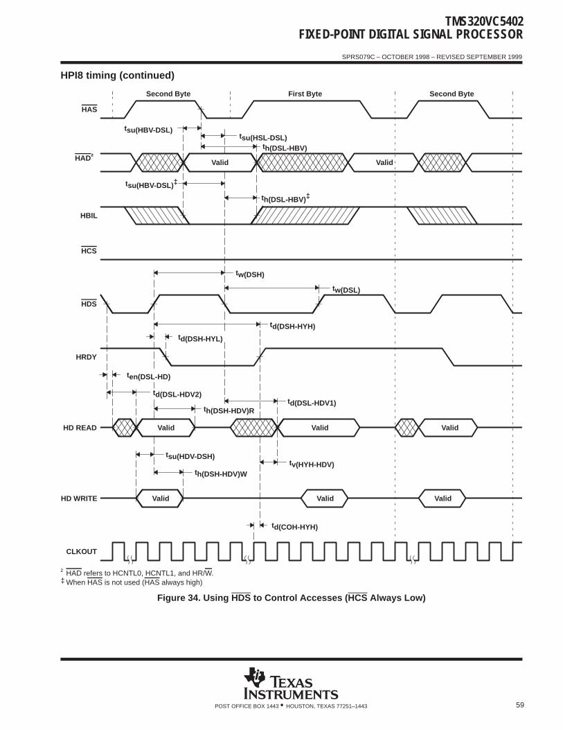
TMS320VC5402FIXED-POINT DIGITAL SIGNAL PROCESSOR
SPRS079C – OCTOBER 1998 – REVISED SEPTEMBER 1999
59POST OFFICE BOX 1443 • HOUSTON, TEXAS 77251–1443
HPI8 timing (continued)
Valid
tsu(HSL-DSL)
Valid
tsu(HBV-DSL)
tsu(HBV-DSL) ‡
HAS
HBIL
th(DSL-HBV)
th(DSL-HBV) ‡
td(DSH-HYH)
tw(DSL)
td(DSL-HDV1)
tv(HYH-HDV)
Valid Valid
Valid
td(COH-HYH)
Valid
tw(DSH)
td(DSH-HYL)
th(DSH-HDV)R
th(DSH-HDV)W
Valid
tsu(HDV-DSH)
td(DSL-HDV2)
ten(DSL-HD)
HCS
HDS
HRDY
HD READ
ValidHD WRITE
CLKOUT
Second Byte First Byte Second Byte
HAD†
† HAD refers to HCNTL0, HCNTL1, and HR/W.‡ When HAS is not used (HAS always high)
Figure 34. Using HDS to Control Accesses (HCS Always Low)
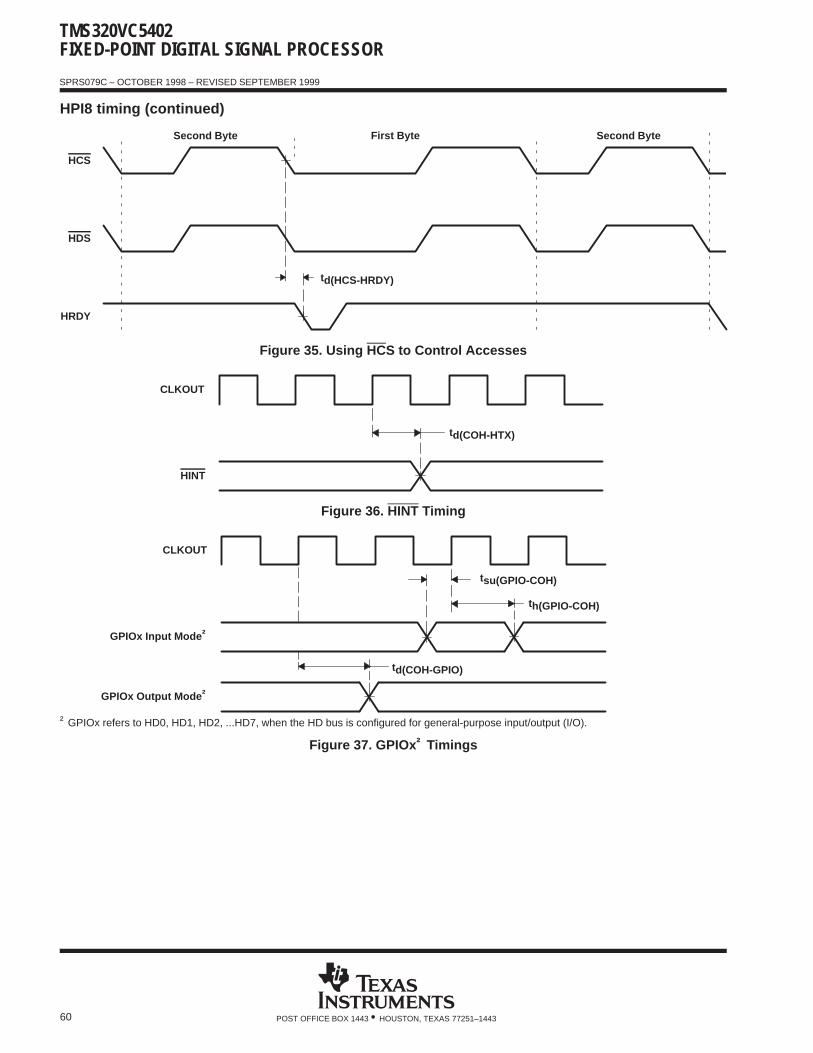
TMS320VC5402FIXED-POINT DIGITAL SIGNAL PROCESSOR
SPRS079C – OCTOBER 1998 – REVISED SEPTEMBER 1999
60 POST OFFICE BOX 1443 • HOUSTON, TEXAS 77251–1443
HPI8 timing (continued)
Second ByteFirst ByteSecond Byte
td(HCS-HRDY)
HCS
HDS
HRDY
Figure 35. Using HC S to Control Accesses
HINT
CLKOUT
td(COH-HTX)
Figure 36. HINT Timing
GPIOx Input Mode †
CLKOUT
th(GPIO-COH)
GPIOx Output Mode †
tsu(GPIO-COH)
td(COH-GPIO)
† GPIOx refers to HD0, HD1, HD2, ...HD7, when the HD bus is configured for general-purpose input/output (I/O).
Figure 37. GPIOx † Timings
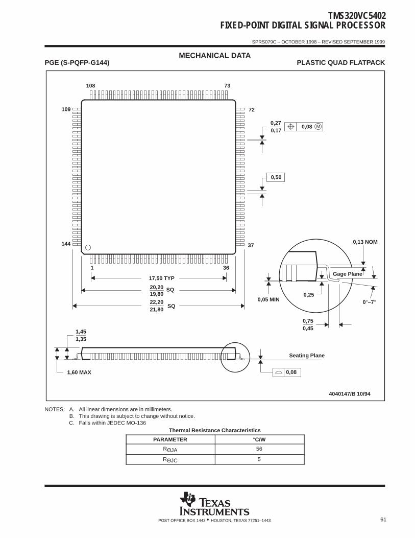
TMS320VC5402FIXED-POINT DIGITAL SIGNAL PROCESSOR
SPRS079C – OCTOBER 1998 – REVISED SEPTEMBER 1999
61POST OFFICE BOX 1443 • HOUSTON, TEXAS 77251–1443
MECHANICAL DATAPGE (S-PQFP-G144) PLASTIC QUAD FLATPACK
4040147/B 10/94
0,27
72
0,17
37
73
0,13 NOM
0,25
0,750,45
0,05 MIN
36
Seating Plane
Gage Plane
108
109
144
SQ
SQ22,2021,80
1
19,80
17,50 TYP
20,20
1,351,45
1,60 MAX
M0,08
0°–7°
0,08
0,50
NOTES: A. All linear dimensions are in millimeters.B. This drawing is subject to change without notice.C. Falls within JEDEC MO-136
Thermal Resistance Characteristics
PARAMETER °C/W
RΘJA 56
RΘJC 5
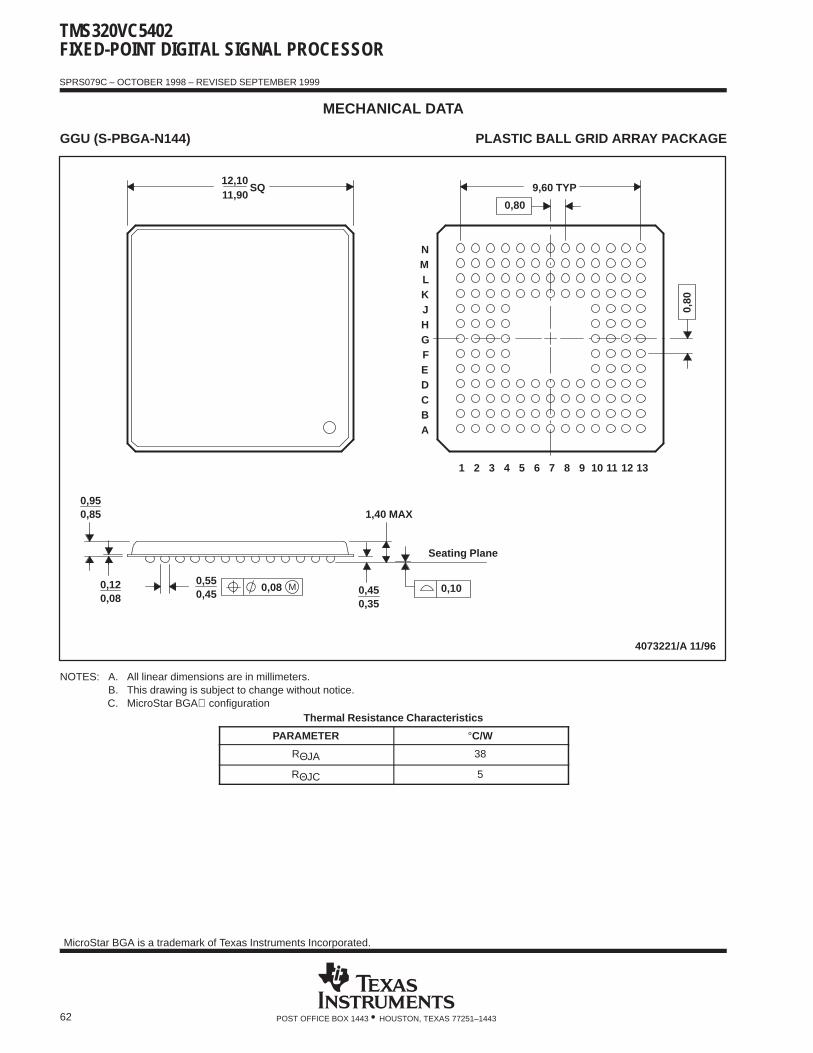
TMS320VC5402FIXED-POINT DIGITAL SIGNAL PROCESSOR
SPRS079C – OCTOBER 1998 – REVISED SEPTEMBER 1999
62 POST OFFICE BOX 1443 • HOUSTON, TEXAS 77251–1443
MECHANICAL DATA
GGU (S-PBGA-N144) PLASTIC BALL GRID ARRAY PACKAGE
0,80
0,10M0,08
0,80
9,60 TYP
12 1310 118 96 7
NM
KL
JH
42 3
FE
CB
D
A
1
G
5
Seating Plane
4073221/A 11/96
SQ11,9012,10
0,95
0,350,450,45
0,55
0,85
0,080,12
1,40 MAX
NOTES: A. All linear dimensions are in millimeters.B. This drawing is subject to change without notice.C. MicroStar BGA configuration
Thermal Resistance Characteristics
PARAMETER °C/W
RΘJA 38
RΘJC 5
MicroStar BGA is a trademark of Texas Instruments Incorporated.
IMPORTANT NOTICE
Texas Instruments and its subsidiaries (TI) reserve the right to make changes to their products or to discontinueany product or service without notice, and advise customers to obtain the latest version of relevant informationto verify, before placing orders, that information being relied on is current and complete. All products are soldsubject to the terms and conditions of sale supplied at the time of order acknowledgement, including thosepertaining to warranty, patent infringement, and limitation of liability.
TI warrants performance of its semiconductor products to the specifications applicable at the time of sale inaccordance with TI’s standard warranty. Testing and other quality control techniques are utilized to the extentTI deems necessary to support this warranty. Specific testing of all parameters of each device is not necessarilyperformed, except those mandated by government requirements.
CERTAIN APPLICATIONS USING SEMICONDUCTOR PRODUCTS MAY INVOLVE POTENTIAL RISKS OFDEATH, PERSONAL INJURY, OR SEVERE PROPERTY OR ENVIRONMENTAL DAMAGE (“CRITICALAPPLICATIONS”). TI SEMICONDUCTOR PRODUCTS ARE NOT DESIGNED, AUTHORIZED, ORWARRANTED TO BE SUITABLE FOR USE IN LIFE-SUPPORT DEVICES OR SYSTEMS OR OTHERCRITICAL APPLICATIONS. INCLUSION OF TI PRODUCTS IN SUCH APPLICATIONS IS UNDERSTOOD TOBE FULLY AT THE CUSTOMER’S RISK.
In order to minimize risks associated with the customer’s applications, adequate design and operatingsafeguards must be provided by the customer to minimize inherent or procedural hazards.
TI assumes no liability for applications assistance or customer product design. TI does not warrant or representthat any license, either express or implied, is granted under any patent right, copyright, mask work right, or otherintellectual property right of TI covering or relating to any combination, machine, or process in which suchsemiconductor products or services might be or are used. TI’s publication of information regarding any thirdparty’s products or services does not constitute TI’s approval, warranty or endorsement thereof.
Copyright 1999, Texas Instruments Incorporated