Embed Size (px)
Citation preview

Product Training Guide
6th Generation Plasma Models
Technical Training Department1925 E. Dominguez StreetLong Beach, CA 90810


Contents
Plasma Model List…………………………4 PCB Locations………………………..…29 G5 And G6 System Comparison………..5 Operation Status Panel LED’s………..30 Overall Block Diagram………………….6~7 Power Down LED (Red Flashing)….....31 HD Digital Assembly Block……………..8 Power Down Defective Points…...…32~33 Y – Drive Block………………………...….9 3 Times Power Down Flashing……....34 X – Drive Block……………………….…..10 8 Times Power Down Flashing……....35 Differences – G5 & G6 Drive…….....11~13 Shutdown Block (Blue Flashing)…....36 X & Y Board Differences – G5 & G6….14 Audio Board Caution……………….….37 Power Supply Map – X & Y Drive…..…15 Operation Without Media Receiver…..38 Scan A & B Block…………………….….16 Power On With No Panel Drive……….39 Scan IC – 43 Inch Models……………18~19 Adjustments……………………….….40~46 Scan IC – 50 Inch Models…………...20~21 How To Clear The History……………..47 Address Circuit Blocks – G6…….…22~25 Panel Factory Mode……………….….48~56 Audio Assembly …………………..…26~27 Disassembly…………………………...57~60 Power Supply Unit…………………..….28 RS232 Connection………………..……61

PLASMA MODEL LIST
Type Model # Media receiver
Plasma Display Speakers Table top
stand43" System PDP4360HD PDPR06U PDP436PU PDPS37LR PDKTS1043" System PDP4361HD PDPR06U PDP436PU PDPS37LR PDKTS1150" System PDP5060HD PDPR06U PDP506PU PDPS38LR PDKTS1050" System PDP5061HD PDPR06U PDP506PU PDPS38LR PDKTS1043" System PRO930HD PROR06U PRO436PU PDPS35LR PDK101350" System PRO1130HD PROR06U PRO506PU PDPS36LR PDK1013
Elite Model
Regular ModelG6
Consumer Models
4

L
G5 & G6 System DiagramG6 HD MODEL
SCAN Y DRIVE HD DIGITA Power Supply X DRIVEPD PD
TEMPSENSOR
PD PD
AND circuitPDDiscrimination
V RST
V OFFSET V SUS
ADRES ADRES ADRES ADRES
PD PD PD PD
HD AUDIO
LED IR
Different Assy Main Device Protection circuit line Serial communication line by models ( Power Down )
LOGIC singal Video / Audio signalCommon use Assy to all of models Video sequnce signal
G4/G5 HD MODEL
ADRES ADRES ADRES ADRESTEMP SENSOR
PD PD PD PD
SCAN Y DRIVE DIGITAL PS X DRIVEPD PD PD PD
AND
PD判別
V OFFSET V SUS
ADRES ADRES ADRES ADRES
PD PD PD PD
LED KEY IRPANEL I/F HD AUDIO
IC3753 VOLUME IC3751
AMP
IC5201
MODULE Ucom
IC3401
SEQUENCE PROCESSOR
LVDSRECEIVER
CPU
IC3001DVI Receiver
LVDSRECEIVER
LVDSRECEIVER
LVDSRECEIVER
IC3156EEPROM
IC3301
FLASH ROM
BUFF
IC3754BACK UPEEPROM
IC3157DAC
VOLUME AMP
DAC
MODULE Ucom
SEQUENCE PROCESSOR
LVDSRECEIVER
CPU
BACKUPEEPROMDVI Receiver
LVDSRECEIVER
LVDSRECEIVER
LVDSRECEIVER
LVDSRECEIVER
LVDSRECEIVER
LVDSRECEIVER
LVDSRECEIVER
EEPROM
FLASH ROM
BUFF
KEYSCAN
5
IC1555Driver IC
IC1501LVDS Receiver (PEE002A-K) (PEE002A-K)
IC1501LVDS Receiver
CN1501
U1681IR Receive unit
V+ADR5
CN1502 50 ADDRESSASSY
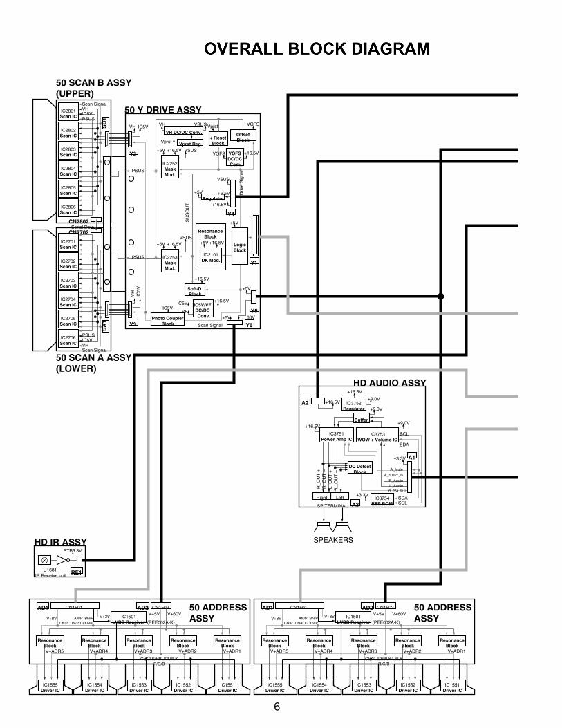
HD AUDIO ASSY
50 SCAN B ASSY(UPPER)
50 Y DRIVE ASSY
50 SCAN A ASSY(LOWER)
HD IR ASSY
ResonanceBlock
IC1554Driver IC
V+ADR4
CLK/LE/HBLK/LBLKR/G/B
V+3V
STB3.3V
RE1
V+8V AN/P BN/PCN/P DN/P CLKN/P
ResonanceBlock
IC1553Driver IC
V+ADR3
V+60V
SP TERMINAL
Right
R_O
UT
+R
_OU
T –
SPEAKERS
V+5V
ResonanceBlock
IC1552Driver IC
V+ADR2
ResonanceBlock
IC1551Driver IC
V+ADR1
ResonanceBlock
L_O
UT
+L_
OU
T –
A3
A2
Y2
Y3
SA
1
AD1 AD2
IC1555Driver IC
CN1501
V+ADR5
CN1502 50 ADDRESSASSY
ResonanceBlock
IC1554Driver IC
V+ADR4
CLK/LE/HBLK/LBLKR/G/B
V+3VV+8V AN/P BN/PCN/P DN/P CLKN/P
ResonanceBlock
IC1553Driver IC
V+ADR3
V+60VV+5V
ResonanceBlock
IC1552Driver IC
V+ADR2
ResonanceBlock
IC1551Driver IC
V+ADR1
ResonanceBlock
AD1 AD2
CN2802
CN2702
Y6
Y5
Y4
Y1
A1
Left
DC DetectBlock
IC3754EEP ROM
IC3751Power Amp IC
IC3752Regulator
Buffer
IC3753WOW + Volume IC
+3.3V
SCL
SCL
SDA
SDA
A_NG_BL_AudioR_Audio
A_STBY_B
A_Mute
+3.3V
+16.5V
IC5V
Driv
e S
igna
l
Vprst
Vprst
PSUS
PSUS
+9.0V
+9.0V
+9.0V
+16.5V
+16.5V
VH VH VSUS
+5V +16.5V+16.5V
VSUS
IC5V
VH
IC2252MaskMod.
Vprst Reg.+ ResetBlock
OffsetBlock
VOFSDC/DC Conv.
+5V
+5V
+16.5V
+5V
+5V
+16.5V+16.5V
+16.5V
Scan Signal
60V
IC5VIC5V
+5V
VOFS
VOFS
VSUS
+16.5V
SU
SO
UT
+6.5V
+5V
VF
VSUS
IC2253MaskMod.
IC2101DK Mod.
ResonanceBlock
LogicBlock
Regulator
Soft-DBlock
IC5V/VFDC/DC Conv.Photo Coupler
Block
VH DC/DC Conv.
SB
1IC2801Scan IC
IC2701Scan IC
IC2702Scan IC
IC2703Scan IC
IC2704Scan IC
IC2705Scan IC
IC2706Scan IC
IC2802Scan IC
IC2803Scan IC
IC2804Scan IC
IC2805Scan IC
IC2806Scan IC
Serial Data
PSUS
Scan SignalVHIC5V
PSUS
Scan SignalVHIC5V
6

(PEE002A-K) (PEE002A-K)IC1501
LVDS ReceiverIC1501
LVDS Receiver
50 X DRIVE ASSY
POWER SUPPLYUNIT
HD DIGITAL ASSY
SUS CLAMP 1ASSY
DVI CONNECTORMDR CONNECTOR
AC INLET
POWER SW
HD LED ASSY
IC1555Driver IC
CN1501
V+ADR5
CN1502 50 ADDRESSASSY
ResonanceBlock
IC1554Driver IC
V+ADR4
CLK/LE/HBLK/LBLKR/G/B
V+3VV+8V AN/P BN/PCN/P DN/P CLKN/P
ResonanceBlock
IC1553Driver IC
V+ADR3
V+60VV+5V
ResonanceBlock
IC1552Driver IC
V+ADR2
ResonanceBlock
IC1551Driver IC
V+ADR1
ResonanceBlock
AD1 AD2
IC1555Driver IC
CN1501
V+ADR5
CN1502 50 ADDRESSASSY
ResonanceBlock
IC1554Driver IC
V+ADR4
CLK/LE/HBLK/LBLKR/G/B
V+3VV+8V AN/P BN/PCN/P DN/P CLKN/P
ResonanceBlock
IC1553Driver IC
V+ADR3
V+60VV+5V
ResonanceBlock
IC1552Driver IC
V+ADR2
ResonanceBlock
IC1551Driver IC
V+ADR1
ResonanceBlock
AD1 AD2
P1
P2P7
P6
P5
P4
D10
D4 D11
D9
D8
D7
P3
VSUS
Switching
Switching
SECONDARY PRIMARY
+16.5V
+16.5V
+8VSTA3.3V
PS_PDEXT_PDRELAY
VSUS_ADJ
VSUS_CONT+60V IC202
+6.5V
V+3V ACT
+16.5V
+16.5V
+16.5V+16.5V VF
+16.5V
: Wire haerness
VRN+5V
+5V
+5V
+5V
+6.5V
V+3V_D
V+1V_D
V+8V
PSIZE
V+8V
DC-DC ConverterModule
(AXY1116)
DAC
Mask
PulseWidth
IC3151(M30620FCPGP)
Module Ucom
IC3401(PEG122C-K)
SequenceProcessor
IC3001
TMDS Receiver
IC3301Flash Memory
Vsus_ADJ
V+8V
V+8V
V+8V
V+8V
V+3V STB REMSTB_MT
LVDS
AUDIO LAUDIO R
PDPS_PWDNSQ_PD
PD_MUTE
XSUS
OR
OR
UARTSW
Q703
PFC Q101Q102Q103
Q704
T702
T902
T101
T502
RY102
Switching
Switching
NEUTRALLIVE
Switching
D109
+390V D103
D107, D108
Q901
Q902
IC101Switching
Switching
Q501
Q502
D5
D6
D3
D2 D1
H DET
Bus BufferBus Buffer
LED_RLED_BREM
SCAN_PDYDRIVE_PDYSUSTN_PDYDD_CNV_PDSCN5V_PD
SCANYSUS
Vofs_ADJ,VYPRST_ADJ
SCL,SCA
RELAY,PD_TRIGGERAC_DET,DRF
XSUSTN_PDXDD_CNV_PDXDRIVE_PD
ADR_PD1
LVDS
VDHDFIELD
SCL, SDASCL, SDA
A_NG
A_MUTE,A_STBY_B
DDCTMDS
DCLK, DERA, GA, BA
VSUS
CL1
SUS CLAMP 2ASSY
VSUS
CL2
L1
X1
LogicBlock
Regulator 15VDC/DC Conv.
IC1101DK Mod.
IC1202MaskMod.
VRNDC/DC Conv.
– ResetBlock
X4 X3
X2
VSUS
VSUS
VSUS
SUS OUT
PSUSDrive Signal
: FFC
7
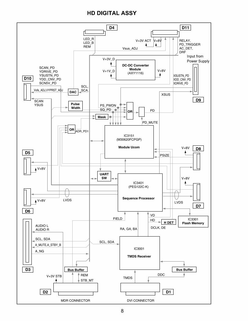
DVI CONNECTORMDR CONNECTOR
D10
D4 D11
D9
D8
D7
V+3V ACT
V+3V_D
V+1V_D
V+8V
PSIZE
V+8V
DC-DC ConverterModule
(AXY1116)
DAC
Mask
PulseWidth
IC3151(M30620FCPGP)
Module Ucom
IC3401(PEG122C-K)
Sequence Processor
IC3001
TMDS Receiver
IC3301Flash Memory
Vsus_ADJ
V+8V
V+8V
V+8V
V+8V
V+3V STB REM
STB_MT
LVDS
AUDIO LAUDIO R
PD
PS_PWDNSQ_PD
PD_MUTE
XSUS
OR
OR
UARTSW
D5
D6
D3
D2 D1
H DET
Bus BufferBus Buffer
LED_RLED_BREM
SCAN_PDYDRIVE_PDYSUSTN_PDYDD_CNV_PDSCN5V_PD
SCANYSUS
Vofs_ADJ,VYPRST_ADJSCL,SCA
RELAY,PD_TRIGGERAC_DET,DRF
XSUSTN_PDXDD_CNV_PDXDRIVE_PD
ADR_PD1
LVDS
VD
HDFIELD
SCL, SDASCL, SDA
A_NG
A_MUTE,A_STBY_B
DDCTMDS
DCLK, DERA, GA, BA
8

Y2
Y3 Y6
Y5
Y4
Y1
IC5V
Driv
e S
igna
l
Vprst
Vprst
PSUS
PSUS
VHVH VSUS
+5V +16.5V+16.5V
VSUS
IC5VVH
IC2252MaskMod.
Vprst Reg.
+ ResetBlock
OffsetBlock
VOFSDC/DC Conv.
+5V
+5V
+16.5V
+5V
+5V
+16.5V+16.5V
+16.5V
Scan Signal
60V
IC5V
IC5V
+5V
VOFS
VOFS
VSUS
+16.5V
SU
SO
UT
+6.5V
+5V
VF
VSUS
IC2253MaskMod.
IC2101DK Mod.
ResonanceBlock
LogicBlock
Regulator
Soft-DBlock
IC5V/VFDC/DC Conv.
Photo CouplerBlock
VH DC/DC Conv.
9

50 X DRIVE, SUS CLAMP 1 and SUS CLAMP 2 ASSYS
50 X DRIVE ASSY
SUS CLAMP 1ASSY
+16.5V
+16.5V
+16.5V
+16.5V VF
+16.5V
VRN+5V
+5V
+5V
+5V
+6.5V
VSUS
CL1
SUS CLAMP 2ASSY
VSUS
CL2
X1
LogicBlock
Regulator15V
DC/DC Conv.
IC1101DK Mod.
IC1202MaskMod.
VRNDC/DC Conv.
– ResetBlock
X4 X3
X2
VSUS
VSUS
VSUS
SUS OUT
PSUSDrive Signal
10

Outline of Differences between G5 and G6 Drive Circuits
1. Y Drive Reset Pulse
G5: 3 times reset pulses --> G6: 1time reset pulse
Purpose: Due to improve the black level.Because Plus Reset voltage on Y Drive Assy is larger than the VSUS voltage,a power regulator for the Plus Reset was added and Mask Circuit was changed to two ways.
Minus reset circuit was also added on Y Drive Assy
2. X & Y Drive Resonance circuit
G5: Discrete & double resonance circuit --> G6: Module IC, single resonance circuit
Purpose: Due to cost down
3. X Drive MASK Module IC
G5: Using 2 ICs --> G6 : Using 1 IC
Purpose: Due to cost down
Because Sustain pulse was slightly changed, SUS-Clamp boards were added.
4. Change of SCAN IC
Purpose: To reduce cost.
5G 6G50" Panasonic AN16021AA AN16025A43" TI SN755866PZP SN755870PZT
11

Difference of waveform between G5 and G6
Reset waveform
3 times reset → 1 time reset (Improve dark brightness)Reset voltage of Y drive (Plus voltage) UPReset voltage of X drive (Minus voltage) DOWN
Sustain waveform
2 step resonance → 1 step resonanceVsus voltage LESSSustain pulse cycle SHORTER
G5 G6
XPSUS XPSUS
SCAN out SCAN out
YPSUS YPSUS
100V/DIV 100V/DIV
100V/DIV 100V/DIV
PSUSPSUS
SUS-G
SUS-U
SUS-B
SUS-D
SUS-G
SUS-U1
SUS-B
SUS-D2
SUS-U2
SUS-D1
①
② ③
①
Pulse width of G5
12

Comparison Drive Assy between G5 and G6 (Block diagram)
SUS B
SUS U2
SUS D2
SUS G
P SUS
Vofs
Y Drive Ass'y
Y SUS MSK
-30V
~-52V
SOFT_D
MASK Module
SUS U1
SUS D1
VF
PR-U
共振2段目
共振1段目
To detecting midpoint voltage circuitPD should occur if this voltage is over or
below from specified value.
Vsus
434:215V
504:223V
Panel
P SUS
Vofs
Y Drive A ss'y SCA N A ss'y
VH130V
SC AN IC
-30V ~-52V
Plus reset voltage G5: VSUS → G6:Reserved power supplySince the value of Plus Reset Voltage became beyond the value of VSUS, Plus Reset connect to PSUS and SUSMSK became two-way.
Panel
SUS B
SUS U2
SUS D2
SUS G
Vsus
223V
X Drive Assy for G5
P SUS
X SUS MSK
MASK Module
SUS U1
SUS D1 1st Resonance
中点電位検出回路へ(既定電圧幅より上がっても下がってもPD)
Vrn
-230V
RN D
2 Step Resonance→1 Step ResonanceDiscreet Structure→DK Module
2nd Resonance
Y Drive Assy for G5
1st Resonance
2nd Resonance
Added circuitfor Minus Reset
Y Drive Assy for G6
To detecting midpoint voltage circuit
DK ModuleY Mask Module
Resonance Module ( DK Module)
X Mask Module
X Drive Assy for G6
13

Board Differences between G5 and G6
G5 X Drive Assy
G6 X Drive Assy
G5 Y Drive Assy
G6 Y Drive Assy
G5 : Two Mask Module ICsG6: One Mask Module IC
G5 :Discrete circuitG6: DK Module IC
G5 :Discrete circuitG6: DK Module IC
14

Power Supply map of X and Y Drive ASSY
to Address Ass'y
5.0V
from P Supply
VSUS 16.5V 6.5V VRN
5.0V 6.5V from P Supply
16.5VVSUS
VOFS5.0V
VFIC5V
Vprst
VH
Y Drive Assy X Drive Assy
Note: to Address Ass'yDC/DC converter, for VOFS, and regulator of VPRST arecontrolled by Electric Volume.
Scan Assy Although, basically, each DC/DC converter for VOFS and VRNis inputted 16.5V, as Vcc, they are not active if VSUS is below 100V
Logic
DKMod.
5V Reg.I
MaskMod.
VOFSDC/DC Conv.
VHDC/DC Conv.
IC5VDC/DC Conv.
Reset
Ofset
ScanLogic
Scan IC
VRNDC/DC Conv.
Logic
DKMod.
MaskMod.
5V Reg.
Reset
15VDC/DC Conv.
VPRSTReg.
15
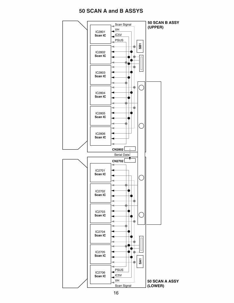
50 SCAN A and B ASSYS
50 SCAN B ASSY(UPPER)
50 SCAN A ASSY(LOWER)
SA
1
CN2802
CN2702
SB
1
IC2801Scan IC
IC2701Scan IC
IC2702Scan IC
IC2703Scan IC
IC2704Scan IC
IC2705Scan IC
IC2706Scan IC
IC2802Scan IC
IC2803Scan IC
IC2804Scan IC
IC2805Scan IC
IC2806Scan IC
Serial Data
PSUS
Scan Signal
VH
IC5V
PSUS
Scan Signal
VH
IC5V
16


SCAN IC - 43 Inch Models
List of ICSN755870PZT, TC7SH08FUS1, TC74VHC00FTS1, AXF1143, AXF1145, TC74VHC08FTS1, AXF1144, M62334FP,TC74VHC123AFTS1, PST3610UR, PEG122C, NJW1183L
SN755870PZT (43 SCAN A ASSY : IC2701 - IC2706)(43 SCAN B ASSY : IC2801 - IC2806)
• Plasma Display Panel IC
Pin Arrangement (Top view)
Block Diagram
1OUT32OUT43OUT54OUT65OUT76OUT87OUT98OUT109OUT1110OUT1211OUT1312OUT1413OUT1514OUT1615OUT1716OUT1817OUT1918OUT2019OUT2120OUT2221OUT2322OUT2423OUT2524OUT2625OUT27
OUT6275OUT6174OUT6073OUT5972OUT5871OUT5770OUT5669OUT5568OUT5467OUT5366OUT5265OUT5164OUT5063OUT4962OUT4861OUT4760OUT4659OUT4558OUT4457OUT4356OUT4255OUT4154OUT4053OUT3952OUT3851
OU
T2
100
OU
T1
99N
.C.
98V
DD
H97
VD
DH
96N
.C.
95G
ND
194
GN
D1
93C
LR92
SI
91O
C2
90O
C1
89V
DD
88LA
T87
CLK
86S
O85
DIR
84G
ND
183
GN
D1
82N
.C.
81V
DD
H80
VD
DH
79N
.C.
78O
UT
6477
OU
T63
76
26O
UT
2827
OU
T29
28O
UT
3029
OU
T31
30O
UT
3231
N.C
.32
VD
DH
33V
DD
H34
N.C
.35
GN
D1
36G
ND
137
GN
D1
38N
.C.
39G
ND
240
GN
D1
41G
ND
142
N.C
.43
VD
DH
44V
DD
H45
N.C
.46
OU
T33
47O
UT
3448
OU
T35
49O
UT
3650
OU
T37
85SO
91SI99
88
1-30,46-76,
100
77
9089
OUT1
GN
D1
GN
D1
GN
D2
OC
2
VD
D
OC
1
VD
DH
VD
DH
OUT2 - OUT63
OUT64
Out
put C
ontr
ol C
ircui
t
64-b
it La
tch
LevelShift
Circuit
DK
Data
Data
DA
LevelShift
Circuit
DK
DA
LevelShift
Circuit
DK
DA
9284
CLRDIR
86
CLK
87
LAT
64-b
it S
hift
Reg
iste
r
18

Pin Function
OC1 OC2 OUT
L L ALL Hi-Z
L H DATA
H L ALL L
H H ALL H
No. Pin Name I/O Pin Function1 - 30 OUT3 - OUT32 O High-voltage push-pull output
31 N.C. − Not connected
32 - 33 VDDH − High-voltage circuit supply
34 N.C. − Not connected
35 - 37 GND1 − Ground
38 N.C. − Not connected
39 GND2 − Ground
40 - 41 GND1 − Ground
42 N.C. − Not connected
43 - 44 VDDH − High-voltage circuit supply
45 N.C. − Not connected
46 - 77 OUT33 - OUT64 O High-voltage push-pull output
78 N.C. − Not connected
79 - 80 VDDH − High-voltage circuit supply
81 N.C. − Not connected
82 - 83 GND1 − Ground
84 DIR ISetup of shift register shift directionL = Shift into reverse (SO → SI) H = Shift forward (SI → SO)
85 SO I/O Serial data input / output
86 CLK I Serial clock input Fetch SI or SO data to shift register by CLK rise edge
87 LAT ILAT data inputL = Transfer shift register data to output latch H = Hold data to output latch
88 VDD − Logic supply
89 OC1 IOutput controlControl output according to the right truth value table
90 OC2 I
91 SI I/O Serial data input / output
92 CLR I All output reset CLR pin : L → Normal operation CLR pin : H → All output High
93 - 94 GND1 − Ground
95 N.C. − Not connected
96 - 97 VDDH − High-voltage circuit supply
98 N.C. − Not connected
99 - 100 OUT1 - OUT2 O High-voltage push-pull output
19

SCAN IC - 50 Inch Models
•
List of ICAN16025A, TC7SH08FUS1, TC74VHC00FTS1, AXF1140, AXF1142, TC74VHC08FTS1, AXF1141, M62334FP,TC74VHC123AFTS1, PST3610UR, PEG122C, NJW1183L
AN16025A (50 SCAN A ASSY : IC2701 - IC2706)(50 SCAN B ASSY : IC2801 - IC2806)
• Plasma Display Panel IC
Pin Arrangement (Top view)
Block Diagram
1OUT32OUT43OUT54OUT65OUT76OUT87OUT98OUT109OUT1110OUT1211OUT1312OUT1413OUT1514OUT1615OUT1716OUT1817OUT1918OUT2019OUT2120OUT2221OUT2322OUT2423OUT2524OUT2625OUT27
OUT6275OUT6174OUT6073OUT5972OUT5871OUT5770OUT5669OUT5568OUT5467OUT5366OUT5265OUT5164OUT5063OUT4962OUT4861OUT4760OUT4659OUT4558OUT4457OUT4356OUT4255OUT4154OUT4053OUT3952OUT3851
OU
T2
100
OU
T1
99N
.C.
98V
DD
H97
VD
DH
96N
.C.
95G
ND
194
GN
D1
93C
LR92
SI
91O
C2
90O
C1
89V
DD
88LA
T87
CLK
86S
O85
DIR
84G
ND
183
GN
D1
82N
.C.
81V
DD
H80
VD
DH
79N
.C.
78O
UT
6477
OU
T63
76
26O
UT
2827
OU
T29
28O
UT
3029
OU
T31
30O
UT
3231
N.C
.32
VD
DH
33V
DD
H34
N.C
.35
GN
D1
36G
ND
137
GN
D1
38N
.C.
39G
ND
240
GN
D1
41G
ND
142
N.C
.43
VD
DH
44V
DD
H45
N.C
.46
OU
T33
47O
UT
3448
OU
T35
49O
UT
3650
OU
T37
85SO
91SI99
88
1-30,46-76,
100
77
9089
OUT1
GN
D1
GN
D1
GN
D2
OC
2
VD
D
OC
1
VD
DH
VD
DH
OUT2 - OUT63
OUT64
Out
put C
ontr
ol C
ircui
t
64-b
it La
tch
LevelShift
Circuit
DK
Data
Data
DA
LevelShift
Circuit
DK
DA
LevelShift
Circuit
DK
DA
9284
CLRDIR
86
CLK
87
LAT
64-b
it S
hift
Reg
iste
r
20

Pin Function
OC1 OC2 OUT
L L ALL Hi-Z
L H DATA
H L ALL L
H H ALL H
No. Pin Name I/O Pin Function1 - 30 OUT3 - OUT32 O High-voltage push-pull output
31 N.C. − Not connected
32 - 33 VDDH − High-voltage circuit supply
34 N.C. − Not connected
35 - 37 GND1 − Ground
38 N.C. − Not connected
39 GND2 − Ground
40 - 41 GND1 − Ground
42 N.C. − Not connected
43 - 44 VDDH − High-voltage circuit supply
45 N.C. − Not connected
46 - 77 OUT33 - OUT64 O High-voltage push-pull output
78 N.C. − Not connected
79 - 80 VDDH − High-voltage circuit supply
81 N.C. − Not connected
82 - 83 GND1 − Ground
84 DIR ISetup of shift register shift directionL = Shift into reverse (SO → SI) H = Shift forward (SI → SO)
85 SO I/O Serial data input / output
86 CLK I Serial clock input Fetch SI or SO data to shift register by CLK rise edge
87 LAT ILAT data inputL = Transfer shift register data to output latch H = Hold data to output latch
88 VDD − Logic supply
89 OC1 IOutput controlControl output according to the right truth value table
90 OC2 I
91 SI I/O Serial data input / output
92 CLR I All output reset CLR pin : L → Normal operation CLR pin : H → All output High
93 - 94 GND1 − Ground
95 N.C. − Not connected
96 - 97 VDDH − High-voltage circuit supply
98 N.C. − Not connected
99 - 100 OUT1 - OUT2 O High-voltage push-pull output
21

<<Feature of G6 address>> <<Change from G5>>Single addressing drive Vadr 61V to 60VOld: 8 PCB (Top side and bottom side) 9V to 8VNew: 4 PCB (Bottom side) 2 connector of Power and SignalAdd TCP heat sink FFC LVDS transmission 3.3V 8V
New TCP (Address IC's) Cord 60V/5VClock frequency:102.5MHz PD circuitDouble edge clock Old: Detecting over current
New: Watching voltage
Simplified Circuit of G6 ADDRESS
Vadr
60V
ADR U
ADR D
ADR B
ADR OUT
ADR Module (TCP)
Panel
ADR PD
Detective circuit
ACTIVE HIGH
22

Digital Assy
60V 60V
5V(Power for TCP)
5V(Power for TCP)
FFC LVDS transmission 3.3V(Power for LVDS receiver) 8V(Power for FET, in address resonance)
Note: 60V(power for Address) and 5V(power for TCP) are supplied through X and Y Drive Assy. The signal of LVDS, 3.3V(power for LVDS receiver) and 8V(power for FET, address resonance) are supplied through Digital Assy.
Simplified Address System Drawing for G6
Address
X-DriveY-Drive
Address Address Address
23

50 ADDRESS ASSY
IC1555Driver IC
IC1501(PEE002A-K)
LVDS Receiver
CN1501
V+ADR5
CN1502
ResonanceBlock
IC1554Driver IC
V+ADR4
CLK/LE/HBLK/LBLKR/G/B
V+3VV+8V AN/P BN/PCN/P DN/P CLKN/P
ResonanceBlock
IC1553Driver IC
V+ADR3
V+60VV+5V
ResonanceBlock
IC1552Driver IC
V+ADR2
ResonanceBlock
IC1551Driver IC
V+ADR1
ResonanceBlock
AD1 AD2
24
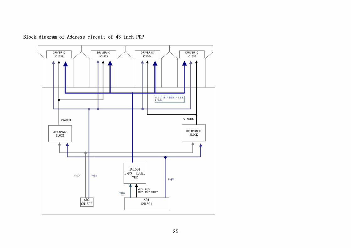
Block diagram of Address circuit of 43 inch PDP
DRIVER ICIC1552
DRIVER ICIC1553
DRIVER ICIC1554
DRIVER ICIC1555
V+ADR1
RESONANCE BLOCK
RESONANCE BLOCK
V+ADR5
AD2CN1502
AD1CN1501
V+60V
V+8V
V+5V
IC1501 LVDS RECEI
VER
V+3V
AN/P BN/P CN/P DN/P CLKN/P
CLK / LE / HBLK / LBLKR/G/B
25

HD AUDIO Assy and other Assy - Differences between G4 / G5 and G6 2005.07.28
1. Change of Surround IC and NJM2195L + BD3869AS NJW1183L SRS IC and VOL IC are changed one chip IC VOL IC (IC3753) due to cost down 2. Change of IC control NJW2195L ⇒ Port control NJW1183L ⇒ IIC Using only IIC control
BD3869AS ⇒ IIC control3. Change of SP terminal AKE1060- AKE1061- G5: Under-Angle type
G6: Straight-Angle type4. Change of AUDIO assembly AUDIO AMP ASS'Y HD AUDIO ASS'Y One board construction due to cost down construction + SP TERMINAL ASS'Y5. EEP ROM for Backup On HD PANEL IF ASS'Y On HD AUDIO ASS'Y Due to deletion of PANEL IF Assy
- Differences between 43 inch and 50 inch : None
- Audio output during Service Factory mode: None
- Other small assemblies:
* LED Assy Change of LED color during Power On ( Green --> Blue )
* IR Assy IR unit was changed to G4 IR unit( No circuit change )
* TEMP SENSOR Assy Move to DIGITAL VIDEO Assy
* KEY Assy Deleted KEY TERMINAL Assy ( Move to front panel of Media Receiver )
Content G4 /G5 AUDIO Assy G6 AUDIO Assy MEMO
26

HD AUDIO ASSY
SP TERMINAL
Right
R_O
UT
+
R_O
UT
–
SPEAKERS
L_O
UT
+
L_O
UT
–
A3
A2
A2
Left
DC DetectBlock
IC3754EEP ROM
IC3751Power Amp IC
IC3752Regulator
Buffer
IC3753WOW + Volume IC
+3.3V
SCL
SCL
SDA
SDA
A_NG_B
L_Audio
R_Audio
A_STBY_B
A_Mute
+3.3V
+16.5V+9.0V
+9.0V
+9.0V
+16.5V
+16.5V
27

POWER SUPPLY UNIT
P1
P2
P7
P6
P5
P4
P3
VSUS
Switching
Switching
SECONDARY PRIMARY
+16.5V
+16.5V
+8VSTA3.3V
PS_PDEXT_PDRELAY
VSUS_ADJ
VSUS_CONT+60V
IC202
+6.5V
Q703
PFC Q101Q102Q103
Q704
T702
T902
T101
T502
RY102
Switching
Switching
NEUTRAL
LIVE
Switching
D109
+390V D103
D107, D108
Q901
Q902
IC101
Switching
Switching
Q501
Q502
28

GENERAL INFORMATION PCB LOCATION
POWER SUPPLY Unit
SUS CLAMP 1 Assy
50 Y DRIVE Assy50 SCAN B Assy
50 SCAN A Assy
HD LEDAssy
HD AUDIO Assy HD DIGITAL Assy SUS CLAMP 2 AssyHD IR Assy
50 ADDRESS Assy50 ADDRESS Assy 50 ADDRESS Assy 50 ADDRESS Assy
50 X DRIVE Assy
29
DIAGNOSIS OF SHUTDOWN/POWER-DOWN INDICATED BY LEDS
BlueRed
Lit in Red1
Lit in Blue2
Red flashes(1000ms)
3
Red andblue flash(1000ms)
4
Red flashes(500+2500ms)
Blue flashes(500+2500ms)
5
6
Lit in Red andblue flashes(200ms)
7
BlueRed
BlueRed
BlueRed
BlueRed
BlueRed
BlueRed
: Lit in Red LED
: Lit in Blue LED
* When a jumper (J110) between the HD AUDIO Assy and the HD DIGITAL Assy is disconnected, the SD LED flashes in this manner.
Note: • When a shutdown occurs, a warning will be issued by the
Media Receiver and displayed, then the power will be shut off.• When a shutdown or power-down occurs on the Panel side,
the Media Receiver will enter Standby mode (the red LED will light).
Standby
Status LED Pattern
Power ON
AC Power OFF ofone side
System cable disconnection
Power-down
Shutdown
No backup copy
• Operation statuses as indicated by LEDs On The Panel
• PD (power-down) count
1000ms
1000ms
500ms
200ms
500ms
Once Once
Once
Twice
Once Twice
1000ms
n times
n times
2.5s
2.5s
1 Not used
2 POWER SUPPLY Unit
3 SCAN Assy
4 5V power supply for SCAN
5 Y-DRIVE
• SD (shut down) count
1 SEQUENCE PROCESSOR (SQ_IC)
2 MDU-IIC
3 RST2 abnormality
4 Panel high temperature
5 Speaker short-circuit *
6 DCDC for Y drive
7 Y-SUS
8 ADDRESS Assy
9 X-DRIVE
10 DCDC for X drive
11 X-SUS
12 Not used
13 Sequence drive stop
14 Not used
15 UNKNOWN
30

Deletion of 16.5 V detection circuit (YDRIVE_PD)
NOTE UVP: Under Voltage Protection, OCP: Over Current Protection
Y Drive PD system(6G)
Middle-point Voltage of resonance
( Sustain )
Comparison to standard
voltage
YSUS_PD
Y_DD_PD
SCAN_PD
SCN5V_PD
IC5V
Detection of SCAN Upperconnection
Voltage Detection
Detection of SCAN Lowerconnection
VOFS
VHUVP
Detection
VPrst
( 3 times PD )
( 4 times PD )
( 5 times PD )
( 6 times PD )
( 7 times PD )
UVPDetection
Voltage Detection
Voltage Detection
X Drive PD system(6G)
XSUS_PD
16.5V XDRIVE_PD
XDD_PDVRN
OCP detection
Deletion of this detection circuit
VF15V
Only detecting disconnection of FFC
( 9 times PD )
( 10 times PD )
( 11 times PD )
UVPDetection
UVPDetection
Comparison to standard
voltage
Middle-point Voltage of resonance
( Sustain )
31
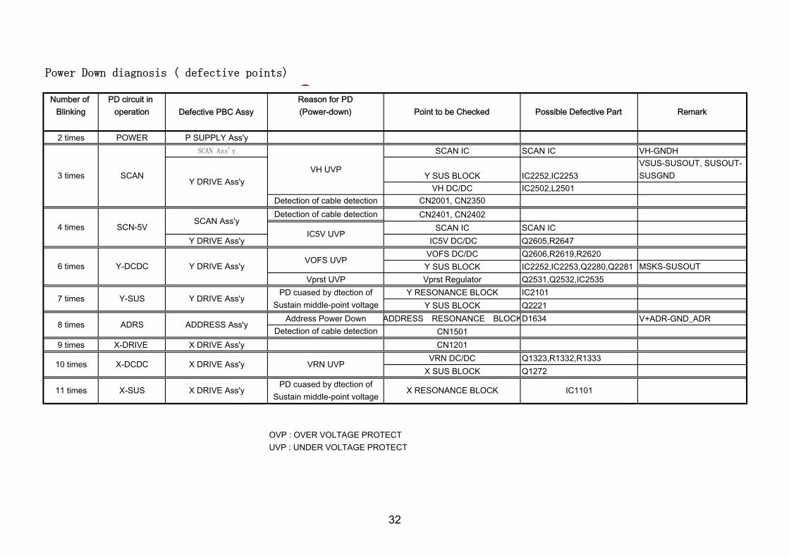
Power Down diagnosis ( defective points)
Number of PD circuit in Reason for PDBlinking operation Defective PBC Assy (Power-down) Point to be Checked Possible Defective Part Remark
2 times POWER P SUPPLY Ass'y SCAN Ass'y SCAN IC SCAN IC VH-GNDH
Y SUS BLOCK IC2252,IC2253VSUS-SUSOUT, SUSOUT-SUSGND
VH DC/DC IC2502,L2501Detection of cable detection CN2001, CN2350Detection of cable detection CN2401, CN2402
SCAN IC SCAN ICY DRIVE Ass'y IC5V DC/DC Q2605,R2647
VOFS DC/DC Q2606,R2619,R2620Y SUS BLOCK IC2252,IC2253,Q2280,Q2281 MSKS-SUSOUT
Vprst UVP Vprst Regulator Q2531,Q2532,IC2535Y RESONANCE BLOCK IC2101
Y SUS BLOCK Q2221Address Power Down ADDRESS RESONANCE BLOCKD1634 V+ADR-GND_ADR
Detection of cable detection CN15019 times X-DRIVE X DRIVE Ass'y CN1201
VRN DC/DC Q1323,R1332,R1333X SUS BLOCK Q1272
OVP : OVER VOLTAGE PROTECTUVP : UNDER VOLTAGE PROTECT
PD cuased by dtection of Sustain middle-point voltage
X RESONANCE BLOCK IC110111 times X-SUS X DRIVE Ass'y
X DRIVE Ass'y
3 times
10 times X-DCDC
6 times
8 times
4 times
ADRS ADDRESS Ass'y
SCN-5V
VRN UVP
VOFS UVP
IC5V UVP
VH UVP
7 times Y-SUS Y DRIVE Ass'yPD cuased by dtection of
Sustain middle-point voltage
SCAN Ass'y
SCAN
Y-DCDC Y DRIVE Ass'y
Y DRIVE Ass'y
32

Assumed symptom from PD mode
Blinking PD circuit Check portion Main symptom Remarks2 Power PD Power Supply
Scan Ass'y Short between VH and GNDH, Scan IC PD with panel briefly flashing Malfunction of DC/DC converter, for VH PD with panel briefly flashing Short between VSUS, SUSOUT, or SUSGND, Mask Module
PD without panel flashing
Disconnect connector between Y Drive and Power Supply, or Digital Assy.
PD without panel flashing
X Drive AssyShort between VSUS, SUSOUT, or SUSGND, Mask Module
PD without panel flashing
SCAN Ass'y Short between IC5V and GNDH, Scan ICDisconnect bridge connector, between Scan Assy and Y Drive, R2352 open (16.5V line resistor) PD without panel flashingMalfunction of DC/DC converter, for IC5V
5 Y-DRIVE PD Delete detection circuitShort between PSUS and MSKS, Mask ModuleShort between MSKS and SUSOUT, Mask Module PD with panel briefly flashing Malfunction of DC/DC converter, for VOFSMalfunction of Regulator of VprstMalfunction of DK moduleControl signal line problem
8 Address PD Address Assy
9 X-DRIVE PD X Drive AssyDisconnect Flexible cable, between Digital Assy and X DriveDisconnect connector between X Drive and Power SupplyMalfunction of DC/DC converter, for VRNR1204 open (16.5V line resistor) PD without panel flashingMalfunction of DK moduleControl signal line problem
Y Drive Assy
Y Drive Assy
6 Y DCDC PD Y Drive Assy
3 SCAN PD
4 IC5V PD
7
10
11 X SUS PD X Drive Assy
X DCDC PD X Drive Assy
Y Drive AssyY SUS PD
33

Diagnosis method for 3 times flashing PD
Diagnose 3 times flashing PD according to the steps below1. Visual check with Power off condition 2. Impedance check with power off condition3. Voltage check with power on condition
Actual diagnosis methods are as follows
1. Visual check with Power off condition
Check the all of connectors and FFC on Y Drive Assy whether completely connected
2. Impedance check with power off condition
i ) Impedance check between Vsus - SUSGND on Power Supply AssyIf the impedance is several hundreds k ohm or over -> go to step " ii "
If the impedance is short circuit -> Remove P1 and P2 connectors and check impedance between Vsus - SUSGND on X Drive and Y Drive Assy.Follow check steps below.
Vsus - SUSGND impedance check on X and Y Drive Assy with no Vsus cables If the impedance on X Drive Assy is short circuit → Replace X Drive Assy
Vsus-SUSOUT or SUSOUT-SUSGND are short circuit : Defective of X MASK module ICOther than above : defective of other devices
If the impedance on Y Drive Assy is short circuit → Replace Y Drive AssyVsus-SUSOUT or SUSOUT-SUSGND are short circuit : Defective of Y MASK module ICOther than above : defective of other devices
If the impedance on Power Supply Assy is short circuit → Replace Power Supply Assy
NOTE: Because some capacitors have voltage, it seems impedance is short just after measuring of impedance by multimeter. Actually if no short circuit , the impedance is soon going up.
ii ) Impedance check between VH - PSUS on Y DRIVE AssyIf the impedance is several M ohm or over -> go to step 3
If the impedance is short circuit -> Remove bridge connectors between Y Drive Assy and Scan A or B Assy and check it again at Y drive, Scan A and Scan B Assy.
Short circuit on Scan A Assy -> Scan IC on Scan A Assy is defective Short circuit on Scan B Assy -> Scan IC on Scan B Assy is defective Short circuit on Y Drive Assy -> Defective of Y Drive Assy
3. Voltage check with power on condition before PD is working
Vsus voltage is not going up to around 200 V -> Defective of Power Supply AssyVH voltage is not going up to around 130 V -> Defective of DC-DC converter on Y Drive Assy
4. Check of Power Down detection circuit
If there is no problem step 1, 2, and 3, both of VH voltage and VSUS voltage are normal, but PD circuit is working. Therefore PD detection circuit has problem. -> Replace Y Drive Assy : because detection circuits for 3 times PD are on Y Drive Assy
34

The list of possible defective parts
(Address PD : Red LED blinks 8 times)
Parts# and markDescription Defective mode
50 inch 43 inchHAT1110R
FETShort or Open between D(Drain) and S(Source)Q1614 etc. Q1609 etc.
UDZS15(B)Zener Diode Short or Open
D1605 etc. D1620 etc.EP05FA20
Diode Short or OpenD1634 etc. D1608 etc.ACH1405 ACH1422 φ10 Chemical
CondenserShort
C1602 etc. C1602 etc.2SA1163
Transistor Short or OpenQ1613 Q1612
RN1901Digital Transistor Short or Open
Q1612 Q1615disconnecting connector FFC disconnecting connector
35
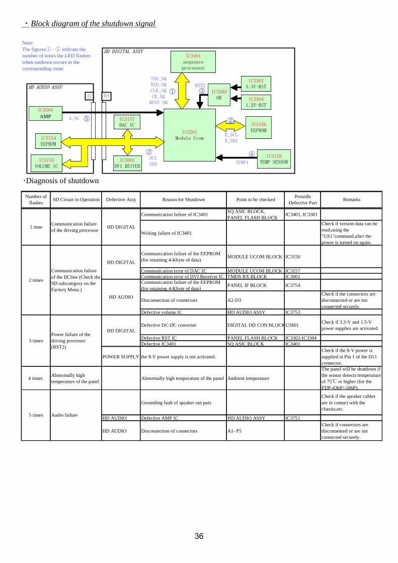
・Block diagram of the shutdown signal
HD DIGITAL ASSY
HD AUDIO ASSY
IC3401sequence processor
IC3156EEPROM
IC3753VOLUME IC
IC3504
AMP
IC3158TEMP SENSOR
IC33023.3V-RST
IC33041.2V-RST
IC3303OR
IC5201Module Ucom
D3①
②
③
④
⑤A_NG
TEMP1
A2
SCLSDA
E_SCLE_SDA
RST2
TXD_SQRXD_SQCLK_SQCE_SQ
BUSY SQ
Note:The figures ① - ⑤ indicate the number of times the LED flashes when sutdown occurs in the corresponding route.
IC3754EEPROM
②
IC3001DVI REIVER
IC3157DAC IC
・Diagnosis of shutdown
Communication failure of IC3401 SQ ASIC BLOCK,PANEL FLASH BLOCK IC3401, IC3301
Writing failure of IC3401
Check if version data can beread,using the"GS1"command,after thepower is turned on again.
Communication failure of the EEPROM(for retaining 4-Kbyte of data) MODULE UCOM BLOCK IC3156
Communication error of DAC IC MODULE UCOM BLOCK IC3157Communication error of DVI Receiver IC TMDS RX BLOCK IC3001Communication failure of the EEPROM(for retaining 4-Kbyte of data) PANEL IF BLOCK IC3754
Disconnection of connectors A2-D3Check if the connectors aredisconnected or are notconnected securely.
Defective volume IC HD AUDIO ASSY IC3753
Defective DC-DC converter DIGITAL DD CON BLOCKU3601 Check if 3.3-V and 1.5-Vpower supplies are activated.
Defective RST IC PANEL FLASH BLOCK IC3302-IC3304Defective IC3401 SQ ASIC BLOCK IC3401
POWER SUPPLY the 8-V power supply is not activated.Check if the 8-V power issupplied at Pin 1 of the D11connector.
4 times Abnormally hightemperature of the panel Abnormally high temperature of the panel Ambient temperature
The panel will be shutdown ifthe sensor detects temperatureof 75℃ or higher (for thePDP-436P/-506P).
Grounding fault of speaker out puts Check if the speaker cablesare in contact with thechassis,etc.
HD AUDIO Defective AMP IC HD AUDIO ASSY IC3751
HD AUDIO Disconnection of connectors A1- P5Check if connectors aredisconnented or are notconnected securely.
Point to be checked PossidleDefective Part RemarksNumber of
flashes SD Cirsuit in Operation Defective Assy Reason for Shutdown
HD DIGITAL
HD AUDIO
HD DIGITAL
HD DIGITAL
Power failure of thedriving processor(RST2)
Communication failureof the IICline (Check theSD subcategory on theFactory Menu.)
Communication failureof the driving processor
Audio failure
1 time
2 times
3 times
5 times
36
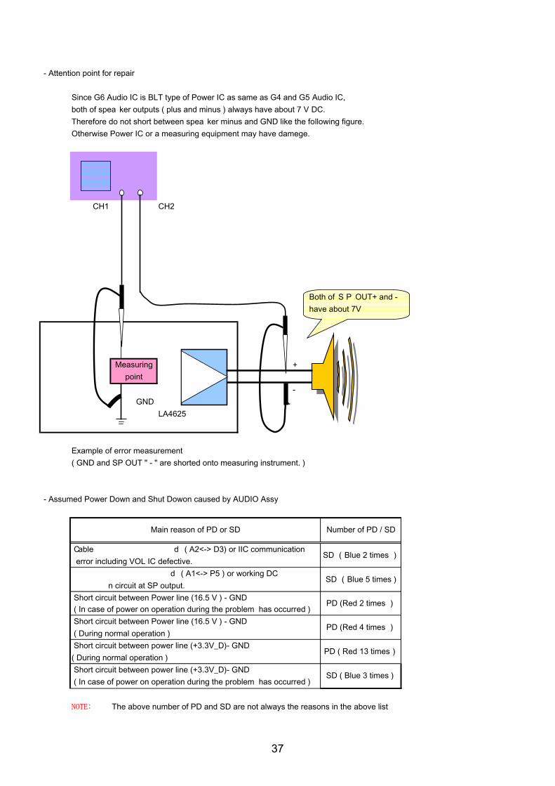
- Attention point for repair
Since G6 Audio IC is BLT type of Power IC as same as G4 and G5 Audio IC, both of speaker outputs ( plus and minus ) always have about 7 V DC. Therefore do not short between speaker minus and GND like the following figure. Otherwise Power IC or a measuring equipment may have damege.
CH1 CH2
+
- GND
LA4625
Example of error measurement( GND and SP OUT " - " are shorted onto measuring instrument. )
- Assumed Power Down and Shut Dowon caused by AUDIO Assy
Cable becomes disconnected ( A2<-> D3) or IIC communication error including VOL IC defective. Cable becomes disconneced ( A1<-> P5 ) or working DC detection circuit at SP output. Short circuit between Power line (16.5 V ) - GND
Short circuit between Power line (16.5 V ) - GND ( During normal operation ) Short circuit between power line (+3.3V_D)- GND( During normal operation ) Short circuit between power line (+3.3V_D)- GND
NOTE: The above number of PD and SD are not always the reasons in the above list
Measuring point
Number of PD / SDMain reason of PD or SD
( In case of power on operation during the problem has occurred )
SD (Blue 2 times )
SD (Blue 5 times )
PD (Red 2 times )
PD (Red 4 times )
PD ( Red 13 times)
( In case of power on operation during the problem has occurred ) SD ( Blue 3 times )
Both of SP OUT+ and -have about 7V
37

OPERATION WHEN THE MEDIA RECEIVER IS NOT CONNECTED
REDREDRED
To operate the panel without the Media Receiver, there are the following two ways:
1. Operation-without-the-Media-Receiver modeInput the "SYS S00" RS232C command. The status of the LEDs changes to that in normal operation mode.Note: Turning the AC switch to OFF then ON also maintains this mode. However, once the unit is connected with the Media Receiver using
the System cable, this mode is automatically canceled.
2. DVI modeTurn the unit on while DVI SG signals are being input with only the DVI connecter connected. After a warning is displayed for about 5 seconds, the unit is ready to display the screen of the input signal. (Blue LED lit)Notes: • Although the output from XGA (43 inch) and WXGA (50 inch) can be input to the unit, this is not a mode open to general users.
(With some signals, errors such as power-down may occur.)
As the connection conditions of the system cables (MDR cable, DVI cable) are usually detected, if no connection, such as cable disconnection, is detected, a warning indication (alternate flashing of the red and blue areas) is displayed on the mask screen, and the red and blue LEDs flash alternately. Then after about 30 seconds, the power is automatically turned off.
Alternate flashing at intervals of about 1 second
BlueBlue
38

POWER ON/OFF FUNCTION FOR THE LARGE-SIGNAL SYSTEM
Function: To prevent a power-down from being generated, operation of only the digital-signal processing and audio circuitsare enabled, and power is not supplied to the panel driving system (large-signal system).
Usages: 1. In a case where a check is required of signals' being correctly output to the driving systems during a repair, etc.2. In a case where diagnosis is required for judging whether the power to the large-signal system or small-signal system has been down when a power-down occurred3. In a case where rewriting of the microcomputer is required
Methods: 1. Short-circuit the points (see Fig. 4 below) on the face and on the reverse side of the HD DIGITAL Assy.2. Issue the "DRV S00" RS-232C command. (Command for turning the function off: DRV S01)
Notes: • When the power to the large-signal system is off, as the PD signal is muted, power-downs other than PS_PD arenot activated.
• As soon as the clips are removed while the power to the large-signal system is off, a power-down will occur. Be sure to turn the power off before removing the clips.
• While this function is activated with RS-232C commands, it is possible to issue "DRV S01" (for turning thefunction off) while the power is on. However, as it may damage the unit, turn the power off before issuing the"DRV S01" command.
• Although the "DRV S00/S01" RS-232C commands are valid during Standby mode, once the main power isturned off, the unit will return to "DRV S01."
Position of DRIVE OFF
Note: It is recommended to use clips like those shown here rather than alligator clips, because alligator clips may not reach the copper foil of the board.
Short-circuit the face and the reverse side, using clips, etc.
39

ADJUSTMENT
ADJUSTMENT REQUIRED WHEN THE SET IS REPAIRED OR REPLACED
1. At shipment, the unit is adjusted to its best conditions. Normally, it is not necessary to readjust even if an assembly is replaced. If the adjustment is shifted or if it becomes necessary to readjust because of part replacement, etc., perform the adjustment as described below.
2. Any value changed in Service/Factory mode will be stored in memory as soon as it is changed. Before readjustment, take note of the original values for reference in case you need to restore the original settings.
3. Use a stable AC power supply.
50 Y DRIVE Assy No adjustment required
POWER SUPPLY Unit No adjustment required
DIGITAL VIDEO Assy Writing of backup data is required. Refer to the "BACKUP WHEN THE MAIN UNIT IS ADJUSTED. "
50 X DRIVE Assy No adjustment required
Other assemblies No adjustment required
Service Panel Refer to the "6.3 METHOD FOR REPLACING THE SERVICE PANEL ASSY."
POWER SUPPLY Unit
DIGITAL VIDEO Assy No adjustment required
No adjustment required
No adjustment required
50 X DRIVE Assy
50 Y DRIVE Assy
Other assemblies No adjustment required
When any of the following assemblies is replaced
When any part in the following assemblies is replaced
The assembly must be replaced as a unit, and no part replacement is allowed.
40

METHOD FOR REPLACING THE SERVICE PANEL ASSY
(Rear of the Panel)
AWU∗∗∗∗Vofs = 35V Vyprst = 270VHour Meter HSpace
AWU∗∗∗∗Vofs = 35V Vyprst = 270VHour Meter H1520
Write in the value for the hourmeter when the Panel is replaced (ex. 1520H).
A .P N E L
L /1[ BT 6 0 V S ]
V –D 1 1 11 6 0 – N T V HJ– S 6F A C T
A J ( + )P N E L – 1 A D
1
5
10
15
16
1 5 10 15 20 25 30 32
A .P N E L
L /1[ BT 6 0 V S ]
V –D 1 1 11 6 0 – N T V HJ– S 6F A C T
O < = >V L R S T P
A JP N E L – 1 A D
5: 0 8
1
5
10
15
16
1 5 10 15 20 25 30 32
A .P N E L
L /1[ BT 6 0 V S ]
V –D 1 1 11 6 0 – N T V HJ– S 6F A C T
T +E C . ( )
1
5
10
15
16
1 5 10 15 20 25 30 32
A .P N E L
L /1[ BT 6 0 V S ]
V –D 1 1 11 6 0 – N T V HJ– S 6F A C T
R O . < = >H - TM R NI F
TE C .
O: N
1
5
10
15
16
1 5 10 15 20 25 30 32
When the Panel Assy is replaced with one for service, the following adjustments are required: Adjustments of Vofs voltage and Vyprst voltageEnter the reference adjustment values for the Vofs voltage and Vyprst voltage that are written on the label attached to the panel for service.Note: Enter the values, using an RS-232C command or the Factory Menu.
Using an RS-232C commandEnter a "PFY" command with Factory mode ON.Convert the adjustment voltage values written on the label attached at the rear of the Panel to an input command, referring to the conversion chart. (See the next page.)• Reference adjustment of the Vofs voltage: Ex. "Vofs = 35" → (Check the conversion chart.) Enter "VOF112."• Reference adjustment of the Vyprst voltage: Ex. 50-inch "Vyprst = 170 V" → (Check the conversion chart.) Enter "VRP055."(Note that the conversion charts for 50-inch and 43-inch Panels are different.)
Clearing data on various histories of the Panel, such as those on the hour meter • It is necessary to clear the data on the hour meter, etc. to match them to the actual driving hours of the Panel. • It is also necessary to clear the data on SD and PD, because the accumulated power-on time when a shutdown or power-
down occurred is recorded.Note: Clear the values, using an RS-232C command or the Factory Menu.
There are two types of hour meters. Do not take the MR hour meter for the hour meter.
Using an RS-232C commandTo acquire the accumulated power-on time of the product itself, use the "GS2" RS-232C command. (See "6.5 Outline of Commands.")1 To clear the data on the hour meter (for the Panel) : CHM2 To clear the data on the pulse meter : CPM3 To clear the data on the SD history : CSD4 To clear the data on the PD history : CPD
Using the Factory Menu
Using the Factory Menu
Select the main item "PANEL FACT." by pressing the MUTE key then enter Panel Factory mode by pressing the SET key. Using the 5/∞ keys, select "PANEL-1 ADJ" then press the SET key to enter the next lower nested layer. Select "VOL-OFFSET" or "VOL RST P" then enter a command value converted from the voltage value, using the 2/3 keys.
In Panel Factory mode, select "ETC" with the 5/∞ keys then press the SET key. Select "HR-MTR INFO" with the 5/∞ keys. Select "CLEAR" with the 2/3 keys then press and hold the SET key for 5 seconds. (The menu automatically returns to the item "ETC".) In the same manner, clear the data by selecting the subcategory items "PM/B1-B5," "PD INFO," and "SD INFO" under "ETC."
41

CommandVoltage value[V]
for common sizesCommon
Voltage value[V] for common sizes
CommonVoltage value[V]
for common sizesCommand
Voltage value[V] for common sizes
CommandVoltage value[V]
for common sizes
VOF000 14.09 VOF056 24.55 VOF112 35.01 VOF168 45.47 VOF224 55.93VOF001 14.28 VOF057 24.74 VOF113 35.20 VOF169 45.66 VOF225 56.12VOF002 14.46 VOF058 24.92 VOF114 35.38 VOF170 45.85 VOF226 56.31VOF003 14.65 VOF059 25.11 VOF115 35.57 VOF171 46.03 VOF227 56.49VOF004 14.84 VOF060 25.30 VOF116 35.76 VOF172 46.22 VOF228 56.68VOF005 15.02 VOF061 25.48 VOF117 35.95 VOF173 46.41 VOF229 56.87VOF006 15.21 VOF062 25.67 VOF118 36.13 VOF174 46.59 VOF230 57.05VOF007 15.40 VOF063 25.86 VOF119 36.32 VOF175 46.78 VOF231 57.24VOF008 15.58 VOF064 26.04 VOF120 36.51 VOF176 46.97 VOF232 57.43VOF009 15.77 VOF065 26.23 VOF121 36.69 VOF177 47.15 VOF233 57.61VOF010 15.96 VOF066 26.42 VOF122 36.88 VOF178 47.34 VOF234 57.80VOF011 16.14 VOF067 26.61 VOF123 37.07 VOF179 47.53 VOF235 57.99VOF012 16.33 VOF068 26.79 VOF124 37.25 VOF180 47.71 VOF236 58.17VOF013 16.52 VOF069 26.98 VOF125 37.44 VOF181 47.90 VOF237 58.36VOF014 16.70 VOF070 27.17 VOF126 37.63 VOF182 48.09 VOF238 58.55VOF015 16.89 VOF071 27.35 VOF127 37.81 VOF183 48.27 VOF239 58.73VOF016 17.08 VOF072 27.54 VOF128 38.00 VOF184 48.46 VOF240 58.92VOF017 17.27 VOF073 27.73 VOF129 38.19 VOF185 48.65 VOF241 59.11VOF018 17.45 VOF074 27.91 VOF130 38.37 VOF186 48.83 VOF242 59.30VOF019 17.64 VOF075 28.10 VOF131 38.56 VOF187 49.02 VOF243 59.48VOF020 17.83 VOF076 28.29 VOF132 38.75 VOF188 49.21 VOF244 59.67VOF021 18.01 VOF077 28.47 VOF133 38.93 VOF189 49.39 VOF245 59.86VOF022 18.20 VOF078 28.66 VOF134 39.12 VOF190 49.58 VOF246 60.04VOF023 18.39 VOF079 28.85 VOF135 39.31 VOF191 49.77 VOF247 60.23VOF024 18.57 VOF080 29.03 VOF136 39.49 VOF192 49.96 VOF248 60.42VOF025 18.76 VOF081 29.22 VOF137 39.68 VOF193 50.14 VOF249 60.60VOF026 18.95 VOF082 29.41 VOF138 39.87 VOF194 50.33 VOF250 60.79VOF027 19.13 VOF083 29.59 VOF139 40.05 VOF195 50.52 VOF251 60.98VOF028 19.32 VOF084 29.78 VOF140 40.24 VOF196 50.70 VOF252 61.16VOF029 19.51 VOF085 29.97 VOF141 40.43 VOF197 50.89 VOF253 61.35VOF030 19.69 VOF086 30.15 VOF142 40.62 VOF198 51.08 VOF254 61.54VOF031 19.88 VOF087 30.34 VOF143 40.80 VOF199 51.26 VOF255 61.72VOF032 20.07 VOF088 30.53 VOF144 40.99 VOF200 51.45VOF033 20.25 VOF089 30.71 VOF145 41.18 VOF201 51.64VOF034 20.44 VOF090 30.90 VOF146 41.36 VOF202 51.82VOF035 20.63 VOF091 31.09 VOF147 41.55 VOF203 52.01VOF036 20.81 VOF092 31.28 VOF148 41.74 VOF204 52.20VOF037 21.00 VOF093 31.46 VOF149 41.92 VOF205 52.38VOF038 21.19 VOF094 31.65 VOF150 42.11 VOF206 52.57VOF039 21.37 VOF095 31.84 VOF151 42.30 VOF207 52.76VOF040 21.56 VOF096 32.02 VOF152 42.48 VOF208 52.94VOF041 21.75 VOF097 32.21 VOF153 42.67 VOF209 53.13VOF042 21.94 VOF098 32.40 VOF154 42.86 VOF210 53.32VOF043 22.12 VOF099 32.58 VOF155 43.04 VOF211 53.50VOF044 22.31 VOF100 32.77 VOF156 43.23 VOF212 53.69VOF045 22.50 VOF101 32.96 VOF157 43.42 VOF213 53.88VOF046 22.68 VOF102 33.14 VOF158 43.60 VOF214 54.06VOF047 22.87 VOF103 33.33 VOF159 43.79 VOF215 54.25VOF048 23.06 VOF104 33.52 VOF160 43.98 VOF216 54.44VOF049 23.24 VOF105 33.70 VOF161 44.16 VOF217 54.63VOF050 23.43 VOF106 33.89 VOF162 44.35 VOF218 54.81VOF051 23.62 VOF107 34.08 VOF163 44.54 VOF219 55.00VOF052 23.80 VOF108 34.26 VOF164 44.72 VOF220 55.19VOF053 23.99 VOF109 34.45 VOF165 44.91 VOF221 55.37VOF054 24.18 VOF110 34.64 VOF166 45.10 VOF222 55.56VOF055 24.36 VOF111 34.82 VOF167 45.29 VOF223 55.75
Conversion chart for the Vofs(Commands vs. common voltage values for the 50-inch and 43-inch models)
<Conversion charts for electronic VRs:Conversion chart for the Vofs>
42

Commonvoltage[V]5
0-inch modele
voltage[V]43-inch
modele Common
voltage[V]50-inch
modele
voltage[V]43-inch
modele Common
voltage[V]50-inch modele
voltage[V]43-inch modele
VRP000 246.3 236.3 VRP056 270.6 260.6 VRP113 295.4 285.4VRP001 246.7 236.7 VRP057 271.0 261.0 VRP114 295.8 285.8VRP002 247.1 237.1 VRP058 271.5 261.5 VRP115 296.2 286.2VRP003 247.6 237.6 VRP059 271.9 261.9 VRP116 296.7 286.7VRP004 248.0 238.0 VRP060 272.3 262.3 VRP117 297.1 287.1VRP005 248.4 238.4 VRP061 272.8 262.8 VRP118 297.5 287.5VRP006 248.9 238.9 VRP062 273.2 263.2 VRP119 298.0 288.0VRP007 249.3 239.3 VRP063 273.6 263.6 VRP120 298.4 288.4VRP008 249.7 239.7 VRP064 274.1 264.1 VRP121 298.8 288.8VRP009 250.2 240.2 VRP065 274.5 264.5 VRP122 299.3 289.3VRP010 250.6 240.6 VRP066 274.9 264.9 VRP123 299.7 289.7VRP011 251.0 241.0 VRP067 275.4 265.4 VRP124 300.1 290.1VRP012 251.5 241.5 VRP068 275.8 265.8 VRP125 300.6 290.6VRP013 251.9 241.9 VRP069 276.2 266.2 VRP126 301.0 291.0VRP014 252.4 242.4 VRP070 276.7 266.7 VRP127 301.4 291.4VRP015 252.8 242.8 VRP071 277.1 267.1 VRP128 301.9 291.9VRP016 253.2 243.2 VRP072 277.5 267.5 VRP129 302.3 292.3VRP017 253.7 243.7 VRP073 278.0 268.0 VRP130 302.7 292.7VRP018 254.1 244.1 VRP074 278.4 268.4 VRP131 303.2 293.2VRP019 254.5 244.5 VRP075 278.9 268.9 VRP132 303.6 293.6VRP020 255.0 245.0 VRP076 279.3 269.3 VRP133 304.0 294.0VRP021 255.4 245.4 VRP077 279.7 269.7 VRP134 304.5 294.5VRP022 255.8 245.8 VRP078 280.2 270.2 VRP135 304.9 294.9VRP023 256.3 246.3 VRP079 280.6 270.6 VRP136 305.3 295.3VRP024 256.7 246.7 VRP080 281.0 271.0 VRP137 305.8 295.8VRP025 257.1 247.1 VRP081 281.5 271.5 VRP138 306.2 296.2VRP026 257.6 247.6 VRP082 281.9 271.9 VRP139 306.7 296.7VRP027 258.0 248.0 VRP083 282.3 272.3 VRP140 307.1 297.1VRP028 258.4 248.4 VRP084 282.8 272.8 VRP141 307.5 297.5VRP029 258.9 248.9 VRP085 283.2 273.2 VRP142 308.0 298.0VRP030 259.3 249.3 VRP087 284.1 274.1 VRP143 308.4 298.4VRP031 259.7 249.7 VRP088 284.5 274.5 VRP144 308.8 298.8VRP032 260.2 250.2 VRP089 284.9 274.9 VRP145 309.3 299.3VRP033 260.6 250.6 VRP090 285.4 275.4 VRP146 309.7 299.7VRP034 261.0 251.0 VRP091 285.8 275.8 VRP147 310.1 300.1VRP035 261.5 251.5 VRP092 286.2 276.2 VRP148 310.6 300.6VRP036 261.9 251.9 VRP093 286.7 276.7 VRP149 311.0 301.0VRP037 262.3 252.3 VRP094 287.1 277.1 VRP150 311.4 301.4VRP038 262.8 252.8 VRP095 287.5 277.5 VRP151 311.9 301.9VRP039 263.2 253.2 VRP096 288.0 278.0 VRP152 312.3 302.3VRP040 263.6 253.6 VRP097 288.4 278.4 VRP153 312.7 302.7VRP041 264.1 254.1 VRP098 288.8 278.8 VRP154 313.2 303.2VRP042 264.5 254.5 VRP099 289.3 279.3 VRP155 313.6 303.6VRP043 264.9 254.9 VRP100 289.7 279.7 VRP156 314.0 304.0VRP044 265.4 255.4 VRP101 290.1 280.1 VRP157 314.5 304.5VRP045 265.8 255.8 VRP102 290.6 280.6 VRP158 314.9 304.9VRP046 266.3 256.3 VRP103 291.0 281.0 VRP159 315.3 305.3VRP047 266.7 256.7 VRP104 291.4 281.4 VRP160 315.8 305.8VRP048 267.1 257.1 VRP105 291.9 281.9 VRP161 316.2 306.2VRP049 267.6 257.6 VRP106 292.3 282.3 VRP162 316.6 306.6VRP050 268.0 258.0 VRP107 292.8 282.8 VRP163 317.1 307.1VRP051 268.4 258.4 VRP108 293.2 283.2 VRP164 317.5 307.5VRP052 268.9 258.9 VRP109 293.6 283.6 VRP165 317.9 307.9VRP053 269.3 259.3 VRP110 294.1 284.1 VRP166 318.4 308.4VRP054 269.7 259.7 VRP111 294.5 284.5 VRP167 318.8 308.8VRP055 270.2 260.2 VRP112 294.9 284.9 VRP168 319.2 309.2
Conversion chart for the Vyprst(Commands vs. voltage values for the 50-inch and 43-inch models)1/2
<Conversion charts for electronic VRs:Conversion chart for the Vyprst>
43

Commonvoltage[V]50-inch modele
voltage[V]43-inch modele
Commonvoltage[V]50-inch modele
voltage[V]43-inch modele
VRP169 319.7 309.7 VRP225 344.0 334.0VRP170 320.1 310.1 VRP226 344.4 334.4VRP171 320.6 310.6 VRP227 344.9 334.9VRP172 321.0 311.0 VRP228 345.3 335.3VRP173 321.4 311.4 VRP229 345.7 335.7VRP174 321.9 311.9 VRP230 346.2 336.2VRP175 322.3 312.3 VRP231 346.6 336.6VRP176 322.7 312.7 VRP232 347.1 337.1VRP177 323.2 313.2 VRP233 347.5 337.5VRP178 323.6 313.6 VRP234 347.9 337.9VRP179 324.0 314.0 VRP235 348.4 338.4VRP180 324.5 314.5 VRP236 348.8 338.8VRP181 324.9 314.9 VRP237 349.2 339.2VRP182 325.3 315.3 VRP238 349.7 339.7VRP183 325.8 315.8 VRP239 350.1 340.1VRP184 326.2 316.2 VRP240 350.5 340.5VRP185 326.6 316.6 VRP241 351.0 341.0VRP186 327.1 317.1 VRP242 351.4 341.4VRP187 327.5 317.5 VRP243 351.8 341.8VRP188 327.9 317.9 VRP244 352.3 342.3VRP189 328.4 318.4 VRP245 352.7 342.7VRP190 328.8 318.8 VRP246 353.1 343.1VRP191 329.2 319.2 VRP247 353.6 343.6VRP192 329.7 319.7 VRP248 354.0 344.0VRP193 330.1 320.1 VRP249 354.4 344.4VRP194 330.5 320.5 VRP250 354.9 344.9VRP195 331.0 321.0 VRP251 355.3 345.3VRP196 331.4 321.4 VRP252 355.7 345.7VRP197 331.8 321.8 VRP253 356.2 346.2VRP198 332.3 322.3 VRP254 356.6 346.6VRP199 332.7 322.7 VRP255 357.0 347.0VRP200 333.2 323.2VRP201 333.6 323.6VRP202 334.0 324.0VRP203 334.5 324.5VRP204 334.9 324.9VRP205 335.3 325.3VRP206 335.8 325.8VRP207 336.2 326.2VRP208 336.6 326.6VRP209 337.1 327.1VRP210 337.5 327.5VRP211 337.9 327.9VRP212 338.4 328.4VRP213 338.8 328.8VRP214 339.2 329.2VRP215 339.7 329.7VRP216 340.1 330.1VRP217 340.5 330.5VRP218 341.0 331.0VRP219 341.4 331.4VRP220 341.8 331.8VRP221 342.3 332.3VRP222 342.7 332.7VRP223 343.1 333.1VRP224 343.6 333.6
Conversion chart for the Vyprst (Commands vs. voltage values for the 50-inch and 43-inch models)2/2
44
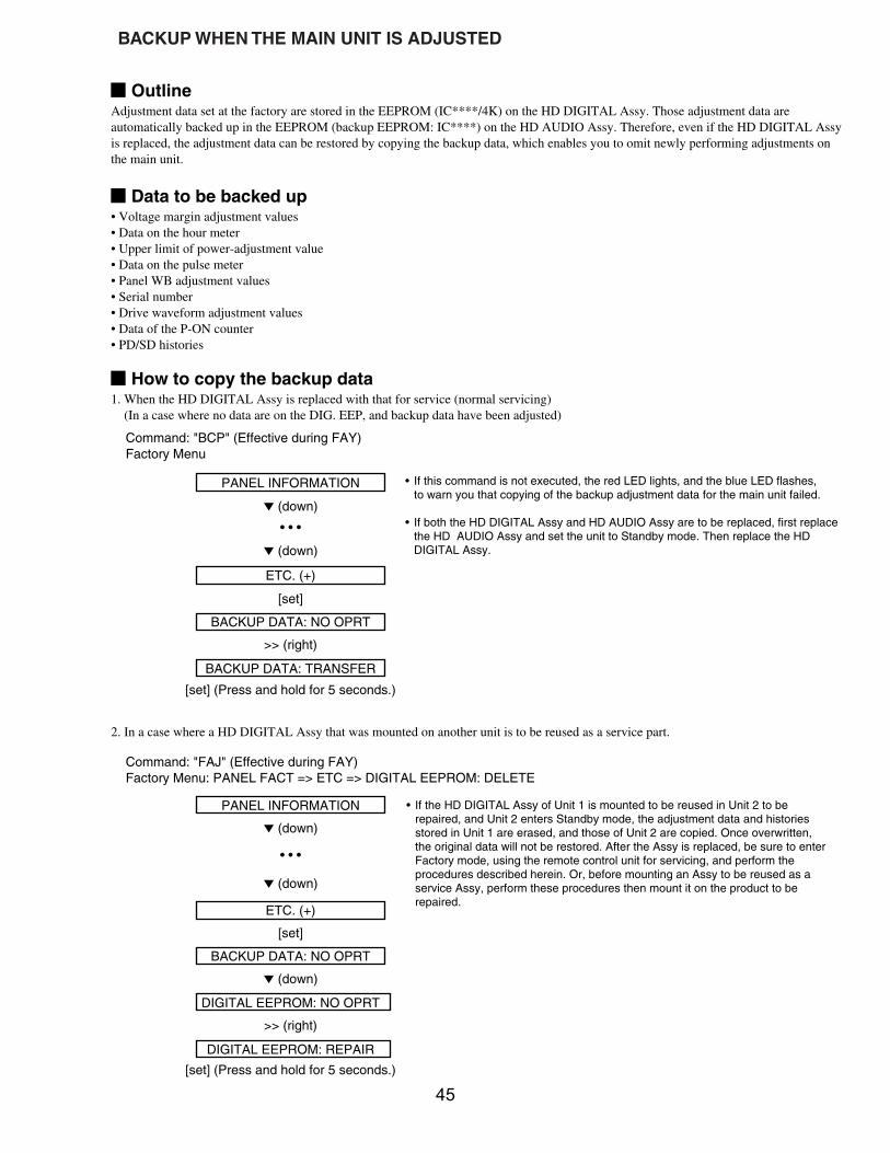
BACKUP WHEN THE MAIN UNIT IS ADJUSTED
• If this command is not executed, the red LED lights, and the blue LED flashes, to warn you that copying of the backup adjustment data for the main unit failed.
• If both the HD DIGITAL Assy and HD AUDIO Assy are to be replaced, first replace the HD AUDIO Assy and set the unit to Standby mode. Then replace the HD DIGITAL Assy.
• If the HD DIGITAL Assy of Unit 1 is mounted to be reused in Unit 2 to be repaired, and Unit 2 enters Standby mode, the adjustment data and histories stored in Unit 1 are erased, and those of Unit 2 are copied. Once overwritten, the original data will not be restored. After the Assy is replaced, be sure to enter Factory mode, using the remote control unit for servicing, and perform the procedures described herein. Or, before mounting an Assy to be reused as a service Assy, perform these procedures then mount it on the product to be repaired.
OutlineAdjustment data set at the factory are stored in the EEPROM (IC****/4K) on the HD DIGITAL Assy. Those adjustment data are automatically backed up in the EEPROM (backup EEPROM: IC****) on the HD AUDIO Assy. Therefore, even if the HD DIGITAL Assy is replaced, the adjustment data can be restored by copying the backup data, which enables you to omit newly performing adjustments on the main unit.
Data to be backed up• Voltage margin adjustment values• Data on the hour meter• Upper limit of power-adjustment value• Data on the pulse meter• Panel WB adjustment values• Serial number• Drive waveform adjustment values• Data of the P-ON counter• PD/SD histories
How to copy the backup data1. When the HD DIGITAL Assy is replaced with that for service (normal servicing) (In a case where no data are on the DIG. EEP, and backup data have been adjusted)
2. In a case where a HD DIGITAL Assy that was mounted on another unit is to be reused as a service part.
Command: "BCP" (Effective during FAY)Factory Menu
Command: "FAJ" (Effective during FAY)Factory Menu: PANEL FACT => ETC => DIGITAL EEPROM: DELETE
PANEL INFORMATION
∞ (down)
• • •
∞ (down)
ETC. (+)
[set]
BACKUP DATA: NO OPRT
>> (right)
[set] (Press and hold for 5 seconds.)
BACKUP DATA: TRANSFER
PANEL INFORMATION
∞ (down)
• • •
∞ (down)
ETC. (+)
[set]
BACKUP DATA: NO OPRT
∞ (down)
DIGITAL EEPROM: NO OPRT
>> (right)
DIGITAL EEPROM: REPAIR
[set] (Press and hold for 5 seconds.)
45

• If the HD DIGITAL Assy with which adjustment data for the main unit have been copied is mounted, the above procedures are not necessary after manual adjustment. (The indication "DIGITAL EEPROM: REPAIR" will not be displayed.)
3. In a case where the HD DIGITAL Assy is replaced with one for servicing because of a defective EEPROM on the original Assy andmanual adjustments are to be performed (in a case where no data are stored in the HD DIGITAL Assy or as backup, and inputadjustment data are to be applied as adjustment data for the main unit)
Command: "UAJ" (Effective during FAY)Factory Menu
PANEL INFORMATION
∞ (down)
• • •
∞ (down)
ETC. (+)
[set]
BACKUP DATA: NO OPRT
∞ (down)
DIGITAL EEPROM: NO OPRT
>> (right)
DIGITAL EEPROM: REPAIR
[set] (Press and hold for 5 seconds.)
46
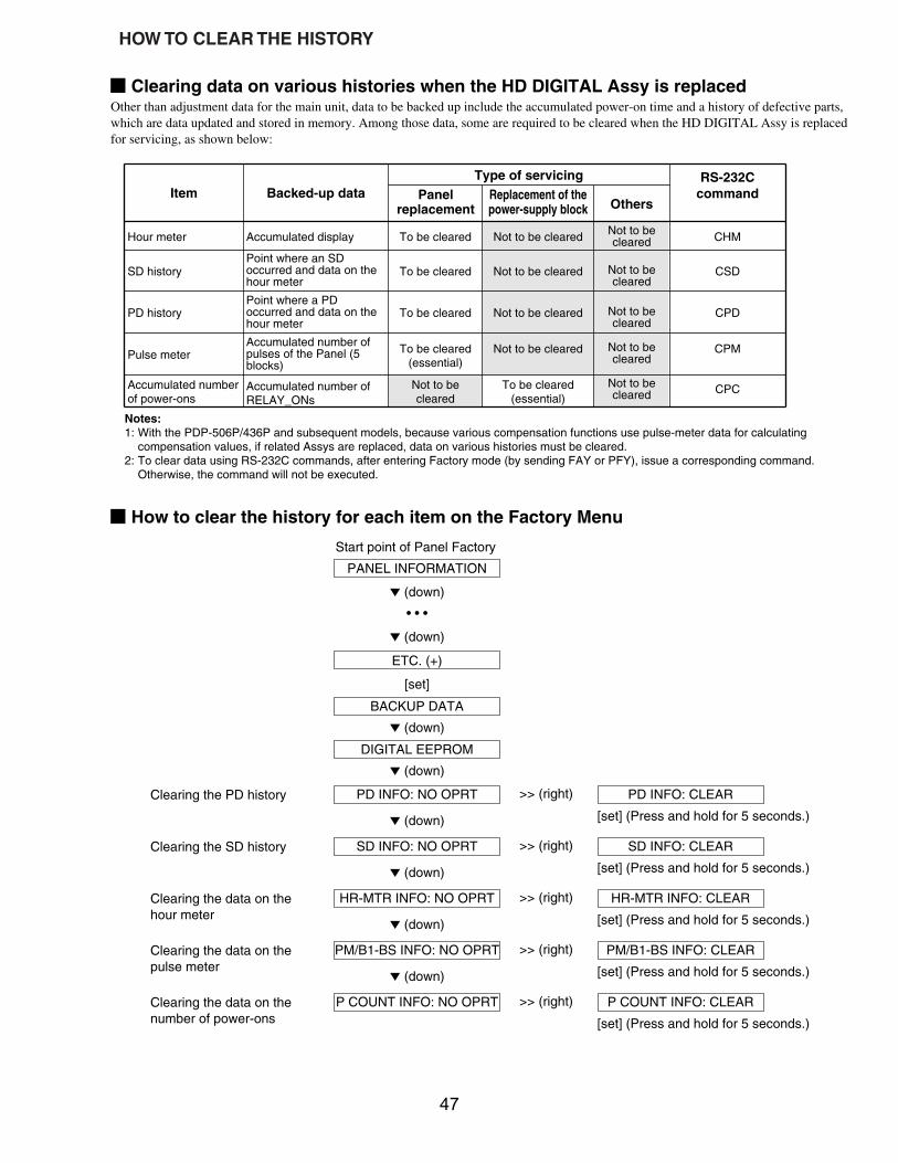
HOW TO CLEAR THE HISTORY
Clearing data on various histories when the HD DIGITAL Assy is replaced
How to clear the history for each item on the Factory Menu
Other than adjustment data for the main unit, data to be backed up include the accumulated power-on time and a history of defective parts, which are data updated and stored in memory. Among those data, some are required to be cleared when the HD DIGITAL Assy is replaced for servicing, as shown below:
Notes:1: With the PDP-506P/436P and subsequent models, because various compensation functions use pulse-meter data for calculating
compensation values, if related Assys are replaced, data on various histories must be cleared.2: To clear data using RS-232C commands, after entering Factory mode (by sending FAY or PFY), issue a corresponding command.
Otherwise, the command will not be executed.
Item Backed-up dataType of servicing RS-232C
commandPanel replacement
Replacement of the power-supply block Others
Hour meter Accumulated display To be cleared Not to be cleared Not to be cleared CHM
SD historyPoint where an SD occurred and data on the hour meter
To be cleared Not to be cleared Not to be cleared
CSD
PD historyPoint where a PD occurred and data on the hour meter
To be cleared Not to be cleared Not to be cleared
CPD
Pulse meterAccumulated number of pulses of the Panel (5 blocks)
To be cleared (essential)
Not to be cleared Not to be cleared
CPM
Accumulated number of power-ons
Accumulated number of RELAY_ONs
Not to be cleared
To be cleared (essential)
Not to be cleared CPC
Start point of Panel Factory
Clearing the PD history
PANEL INFORMATION
∞ (down)
• • •
∞ (down)
∞ (down)
ETC. (+)
[set]
BACKUP DATA
∞ (down)
DIGITAL EEPROM
∞ (down)
PD INFO: NO OPRT PD INFO: CLEAR>> (right)
[set] (Press and hold for 5 seconds.)
Clearing the SD history
∞ (down)
SD INFO: NO OPRT SD INFO: CLEAR>> (right)
[set] (Press and hold for 5 seconds.)
Clearing the data on the hour meter
∞ (down)
HR-MTR INFO: NO OPRT HR-MTR INFO: CLEAR>> (right)
[set] (Press and hold for 5 seconds.)
Clearing the data on the pulse meter
∞ (down)
PM/B1-BS INFO: NO OPRT PM/B1-BS INFO: CLEAR>> (right)
[set] (Press and hold for 5 seconds.)
Clearing the data on the number of power-ons
P COUNT INFO: NO OPRT P COUNT INFO: CLEAR>> (right)
[set] (Press and hold for 5 seconds.)
47

OVERVIEW OF PANEL FACTORY MODE
MR INFORMATION
< MUTE > key
FUNC. CHECK
< MUTE > key
COMMON ADJ.
< MUTE > key
PANEL FACTORY
< SET > key
A .P N E L
AP N E L NI F O R AM
OM D U L E – 0 1 MS 0 S1ES Q – P GR – 0 1 MAQS – D T V– 5 2 0 WQS – D T P– 5 2 0 W
ID G . E PE A D J SU T DEAB C K U P N O AD T !A
ES R I A L _ _ _ __ _ _ _ __ _ _ _ __
0 A2
T I O N
I –N 1 5 20 6 0 – R G B HE– S 6F A C T1
5
10
15
16
1 5 10 15 20 25 30 32
123456789ABCDE
AREA
Note: With this model, the structure of Factory mode has been changed, and all items related to the Panel are gathered into PANEL FACTORY mode.
If a Panel of Generation 6 is connected, "6" is indicated here.
1024 x 672
Top screen of the Factory Menu
48

No.Submode Name
Adjustable Range RemarksSubmode Items
1 PANEL INFORMATION
2 PANEL WORKS
3 POWER DOWN
4 SHUT DOWN
5 PANEL-1 ADJ (+)
5-1 X-SUS B <=> 120 to 136 Equivalent to XSB
5-2 Y-SUS B <=> 120 to 136 Equivalent to YSB
5-3 Y-SUSTAIL T <=> 120 to 136 Equivalent to YTG
5-4 Y-SUSTAIL W <=> 120 to 136 Equivalent to YTW
5-5 XY-RST W <=> 120 to 136 Equivalent to RSW
5-6 VOL SUS <=> 000 to 255 Equivalent to VSU
5-7 VOL OFFSET <=> 000 to 255 Equivalent to VOF
5-8 VOL RST P <=> 000 to 255 Equivalent to VRP
5-9 SUS FREQ. <=> MODE1 to MODE8 Equivalent to SFR
6 PANEL-2 ADJ (+)
6-1 R-HIGH <=> 000 to 511 Equivalent to PRH
6-2 G-HIGH <=> 000 to 511 Equivalent to PGH
6-3 B-HIGH <=> 000 to 511 Equivalent to PBH
6-4 R-LOW <=> 000 to 999 Equivalent to PRL
6-5 G-LOW <=> 000 to 999 Equivalent to PGL
6-6 B-LOW <=> 000 to 999 Equivalent to PBL
6-7 ABL <=> 000 to 255 Equivalent to ABL
7 PANEL REVISE
7-1 R-LEVEL <=> LV-0 to LV-7 Equivalent to RRL
7-2 G-LEVEL <=> LV-0 to LV-7 Equivalent to RGL
7-3 B-LEVEL <=> LV-0 to LV-7 Equivalent to RBL
8 ETC (+)
8-1 BACKUP DATA <=> NO OPRT<=>TRANSFER or ERR Equivalent to BCP
8-2 DIGITAL EEPROM <=> NO OPRT<=>DELETE/REPAIR Equivalent to FAJ/UAJ
8-3 PD INFO. <=> NO OPRT <=>CLEAR Equivalent to CPD
8-4 SD INFO. <=> NO OPRT <=>CLEAR Equivalent to CSD
8-5 HR-MTR INFO. <=> NO OPRT <=>CLEAR Equivalent to CHM
8-6 PM/B1-B5 <=> NO OPRT <=>CLEAR Equivalent to CPM
8-7 P-COUNT INFO. <=> NO OPRT <=>CLEAR Equivalent to CPC
9 MASK SETUP (+)
9-1 MASK OFF Equivalent to MKS+S00
9-2 SGL MASK 01 <=> Equivalent to MKS+S01
9-3 SGL MASK 02 <=>
<=>V48<=>V50<=>V60<=>P60<=>P70<=>V72<=>V75<=>
Equivalent to MKS+S02
• • • • • •
9-62 CMB MASK 08 <=> Equivalent to MKC+S08
9-63 CMB MASK 09 <=> Equivalent to MKC+S09
7 Configuration of Panel Factory mode
49
1. PANEL INFORMATION
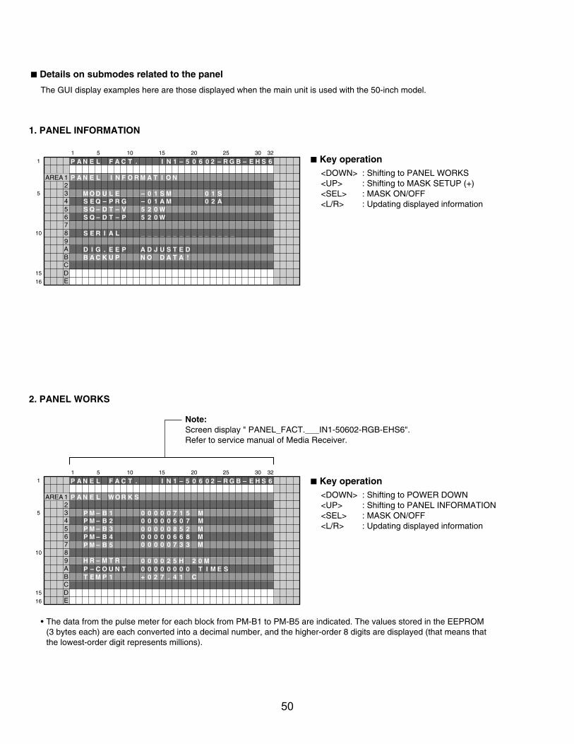
The GUI display examples here are those displayed when the main unit is used with the 50-inch model.
• The data from the pulse meter for each block from PM-B1 to PM-B5 are indicated. The values stored in the EEPROM(3 bytes each) are each converted into a decimal number, and the higher-order 8 digits are displayed (that means that the lowest-order digit represents millions).
<DOWN> : Shifting to PANEL WORKS<UP> : Shifting to MASK SETUP (+)<SEL> : MASK ON/OFF<L/R> : Updating displayed information
A .P N E L
AP N E L NI F O R AM
OM D U L E – 0 1 MS 0 S1ES Q – P GR – 0 1 MAQS – D T V– 5 2 0 WQS – D T P– 5 2 0 W
ID G . E PE A D J SU T DEAB C K U P N O AD T !A
ES R I A L _ _ _ __ _ _ _ __ _ _ _ __
0 A2
T I O N
I –N 1 5 20 6 0 – R G B HE– S 6F A C T1
5
10
15
16
1 5 10 15 20 25 30 32
123456789ABCDE
AREA
2. PANEL WORKS
A .P N E L
AP N E L OW R K S
MP – B 1 0 0 0 00MP – B 2 0 0 0 00
7 516 7
MM0
0 0 0 000 0 0 00
8 256 8
MM6
0 0 0 00 7 3 M3
0 0 0 20 5 0 M2H
MP – B 3MP – B 4MP – B 5
–P C O U TN 0 0 0 00 0 00 IT M SEET M P 1 + 0 .72 4 C1
RH – M T R
I –N 1 5 20 6 0 – R G B HE– S 6F A C T1
5
10
15
16
1 5 10 15 20 25 30 32
123456789ABCDE
AREA
7 Details on submodes related to the panel
7 Key operation
<DOWN> : Shifting to POWER DOWN<UP> : Shifting to PANEL INFORMATION<SEL> : MASK ON/OFF<L/R> : Updating displayed information
7 Key operation
Note:Screen display " PANEL_FACT.___IN1-50602-RGB-EHS6".Refer to service manual of Media Receiver.
50

3. POWER DOWN
• Basically, data acquired with the command QPD are displayed in the columns "1ST" and "2ND, with the values from thehour meter when the power-down occurred.
<Causes of power-down and corresponding OSD indications>
A .P N E L
OP W E R OD WS1 T N2 D
N 1 420 00
1 – – – ––2 Y – S SU
X – D VRS Q – O
–O
–N–N
N3 S C A N – – – –45
7
P OW RE–
S Q – N– – – –
S–
–––
–X – S U– – – –
8
6 S C N 5 VS Q – N NO
A D R S
H 2 3 M
1 420 00 H 2 1 M1 510 00 H 0 5 M1 700 00 H 5 3 M0 890 00 H 4 7 M0 150 00 H 3 0 M0 220 00 H 2 1 M0 000 00 H 5 7 M
H M
I –N 1 5 20 6 0 – R G B HE– S 6F A C T1
5
10
15
16
1 5 10 15 20 25 30 32
123456789ABCDE
AREA
Cause of power-down OSD Indication Cause of power-down OSD Indication
POWER SUPPLY Unit P-PWR ADDRESS Assy ADRS
SCAN Assy SCAN X-DRIVE Assy X-DRV
5V power for SCAN SCN5V DCDC for X drive X-DCDC
Y-DRIVE Assy Y-DRV X-SUS X-SUS
DCDC for Y drive Y-DCDC Sequence drive stopped SQ-NON
Y-SUS Y-SUS UNKNOWN UNKNOW
4. SHUT DOWN
• Basically, data acquired with the command QSD (for MDU-IIC, subcategory data are also displayed) are displayed withthe values from the hour meter when the shutdown occurred.
<Causes of shutdown and corresponding OSD indications>
A .P N E L
HS U T OD WAM I N US B
N 1 420 00
1 – – – ––2 A U D OI
T E M 1P– – – –
O–
––M–
–3 M D – I I C E E P R45
7
S Q – CI – – – –V O L I C
8
6M D – I I C
H 2 3 M
1 420 00 H 2 1 M1 510 00 H 0 5 M1 700 00 H 5 3 M0 890 00 H 4 7 M0 150 00 H 3 0 M
H MH MH M
I –N 1 5 20 6 0 – R G B HE– S 6F A C T1
5
10
15
16
1 5 10 15 20 25 30 32
123456789ABCDE
AREA
Cause of shutdown (main) OSD Indication Cause of shutdown (sub) OSD Indication
SEQUENCE PROCESSOR SQ-IC EEPROM EEPROM
MDU-IIC MDU-IIC BACKUP BACKUP
Abnormality in RST2 RST2 DAC DAC
Panel having high temperature TEMP1 Audio IC VOL-IC
Short-circuited speaker AUDIO DVI DVI
<DOWN> : Shifting to SHUTDOWN<UP> : Shifting to PANEL WORKS<SEL> : MASK ON/OFF<L/R> : Updating displayed information
7 Key operation
<DOWN> : Shifting to PANEL-2ADJ (+)<UP> : Shifting to POWER DOWN<SEL> : MASK ON/OFF<L/R> : Updating displayed information
7 Key operation
51
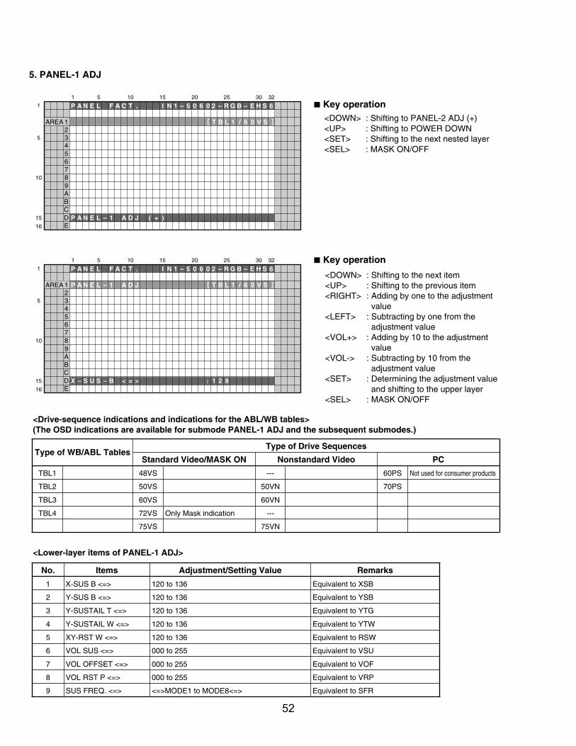
5. PANEL-1 ADJ
<Drive-sequence indications and indications for the ABL/WB tables>(The OSD indications are available for submode PANEL-1 ADJ and the subsequent submodes.)
<Lower-layer items of PANEL-1 ADJ>
A .P N E L
L /1[ BT 6 0 V S ]
I –N 1 5 20 6 0 – R G B HE– S 6F A C T
A JP N E L – 1 A D )( +
1
5
10
15
16
1 5 10 15 20 25 30 32
123456789ABCDE
AREA
<DOWN> : Shifting to the next item<UP> : Shifting to the previous item<RIGHT> : Adding by one to the adjustment
value<LEFT> : Subtracting by one from the
adjustment value<VOL+> : Adding by 10 to the adjustment
value<VOL-> : Subtracting by 10 from the
adjustment value<SET> : Determining the adjustment value
and shifting to the upper layer<SEL> : MASK ON/OFF
A .P N E L
L /1[ BT 6 0 V S ]
I –N 1 5 20 6 0 – R G B HE– S 6F A C T
– >X S U S – B < =
A JP N E L – 1 A D
2: 1 8
1
5
10
15
16
1 5 10 15 20 25 30 32
123456789ABCDE
AREA
Type of WB/ABL TablesType of Drive Sequences
Standard Video/MASK ON Nonstandard Video PC
TBL1 48VS --- 60PS Not used for consumer products
TBL2 50VS 50VN 70PS
TBL3 60VS 60VN
TBL4 72VS Only Mask indication ---
75VS 75VN
No. Items Adjustment/Setting Value Remarks
1 X-SUS B <=> 120 to 136 Equivalent to XSB
2 Y-SUS B <=> 120 to 136 Equivalent to YSB
3 Y-SUSTAIL T <=> 120 to 136 Equivalent to YTG
4 Y-SUSTAIL W <=> 120 to 136 Equivalent to YTW
5 XY-RST W <=> 120 to 136 Equivalent to RSW
6 VOL SUS <=> 000 to 255 Equivalent to VSU
7 VOL OFFSET <=> 000 to 255 Equivalent to VOF
8 VOL RST P <=> 000 to 255 Equivalent to VRP
9 SUS FREQ. <=> <=>MODE1 to MODE8<=> Equivalent to SFR
<DOWN> : Shifting to PANEL-2 ADJ (+)<UP> : Shifting to POWER DOWN<SET> : Shifting to the next nested layer<SEL> : MASK ON/OFF
7 Key operation
7 Key operation
52

6. PANEL-2 ADJ
<Lower-layer items of PANEL-2 ADJ>
A .P N E L
L /1[ BT 6 0 V S ]
I –N 1 5 20 6 0 – R G B HE– S 6F A C T
A JP N E L – 2 A D )( +
1
5
10
15
16
1 5 10 15 20 25 30 32
123456789ABCDE
AREA
A .P N E L
L /1[ BT 6 0 V S ]
I –N 1 5 20 6 0 – R G B HE– S 6F A C T
– >R H I G H < =
A JP N E L – 2 A D
5: 2 6
1
5
10
15
16
1 5 10 15 20 25 30 32
123456789ABCDE
AREA
No. Items Adjustment/Setting Value Remarks
1 R-HIGH <=> 000 to 511 Equivalent to PRH
2 G-HIGH <=> 000 to 511 Equivalent to PGH
3 B-HIGH <=> 000 to 511 Equivalent to PBH
4 R-LOW <=> 000 to 999 Equivalent to PRL
5 G-LOW <=> 000 to 999 Equivalent to PGL
6 B-LOW <=> 000 to 999 Equivalent to PBL
7 ABL <=> 000 to 255 Equivalent to ABL
<DOWN> : Shifting to the next item<UP> : Shifting to the previous item<RIGHT> : Adding by one to the adjustment
value<LEFT> : Subtracting by one from the
adjustment value<VOL+> : Adding by 10 to the adjustment
value<VOL-> : Subtracting by 10 from the
adjustment value<SET> : Determining the adjustment value
and shifting to the upper layer<SEL> : MASK ON/OFF
<DOWN> : Shifting to PANEL REVISE<UP> : Shifting to PANEL-1 ADJ (+)<SEL> : MASK ON/OFF<SET> : Shifting to the next nested layer
7 Key operation
7 Key operation
53
7. PANEL REVISE
<Lower-layer items of PANEL REVISE>
A .P N E L
L /1[ BT 6 0 V S ]
I –N 1 5 20 6 0 – R G B HE– S 6F A C T
A SP N E L E ER V I )( +
1
5
10
15
16
1 5 10 15 20 25 30 32
123456789ABCDE
AREA
A .P N E L
L /1[ BT 6 0 V S ]
I –N 1 5 20 6 0 – R G B HE– S 6F A C T
– –>R L LE V E < =
A S EP N E L ER V I
V: L 0
1
5
10
15
16
1 5 10 15 20 25 30 32
123456789ABCDE
AREA
No. Items Adjustment/Setting Value Remarks
1 R-LEVEL <=> <=>LV-0 to LV-7<=> Equivalent to RRL
2 G-LEVEL <=> <=>LV-0 to LV-7<=> Equivalent to RGL
3 B-LEVEL <=> <=>LV-0 to LV-7<=> Equivalent to RBL
<DOWN> : Shifting to ETC.(+)<UP> : Shifting to PANEL-2 ADJ (+)<SEL> : MASK ON/OFF<SET> : Shifting to the next nested layer
7 Key operation
<DOWN> : Shifting to the next item<UP> : Shifting to the previous item<RIGHT> : Adding by one to the adjustment
value<LEFT> : Subtracting by one from the
adjustment value<VOL+> : Adding by 10 to the adjustment
value<VOL-> : Subtracting by 10 from the
adjustment value<SET> : Determining the setting value
and shifting to the upper layer<SEL> : MASK ON/OFF
7 Key operation
54

8. ETC.
<Lower-layer items of ETC.>
• "NO OPRT" is selected when this submode is entered (to avoid accidental misoperation).• When each item is set, the process starts then the unit shifts to the upper layer. (When NO OPRT is determined,
the unit will shift to the upper layer without doing anything.)• When data are set to be backed up, if the digital EEPROM has not been adjusted,
do the operation of LED pattern No. 7.
A .P N E L
L /1[ BT 6 0 V S ]
I –N 1 5 20 6 0 – R G B HE– S 6F A C T
TE C . )( +
1
5
10
15
16
1 5 10 15 20 25 30 32
123456789ABCDE
AREA
A .P N E L
L /1[ BT 6 0 V S ]
I –N 1 5 20 6 0 – R G B HE– S 6F A C T
A P R O MB C K U P E E >< =
TE C .
O: N P R TO
1
5
10
15
16
1 5 10 15 20 25 30 32
123456789ABCDE
AREA
<DOWN> : Shifting to MASK SETUP (+)<UP> : Shifting to PANEL REVISE (+)<SEL> : MASK ON/OFF<SET> : Shifting to the next nested layer
7 Key operation
<DOWN> : Shifting to the next item<UP> : Shifting to the previous item<RIGHT> : Adding by one to the adjustment
value<LEFT> : Subtracting by one from the
adjustment value<SET> : Determining the setting value
and shifting to the upper layer<SEL> : MASK ON/OFF
7 Key operation
No. Items Adjustment/Setting Value Remarks
1 BACKUP DATA <=> <=>NO OPRT<=>TRANSFER<=>
"ERR" is indicated when no data are in the backup EEPROM. To activate the option to select TRANSFER, press the SET key about 5 seconds.(There is a situation resting more than 5 seconds.)
2 DIGITAL EEPROM <=> <=>NO OPRT<=>REPAIR/DELETE<=>
"DELETE" is indicated when the main unit has been already adjusted. To activate the option to select REPAIR/DELETE, press the SET key about 5 seconds.(There is a situation resting more than 5 seconds.)
3 PD INFO. <=> <=>NO OPRT<=>CLEAR<=>
To activate the option to select CLEAR, repeatedly press the SET key about 5 seconds.(There is a situation resting more than 5 seconds.)
4 SD INFO. <=> <=>NO OPRT<=>CLEAR<=>
5 HR-MTR INFO. <=> <=>NO OPRT<=>CLEAR<=>
6 PM/B1-B5 <=> <=>NO OPRT<=>CLEAR<=>
7 P-COUNT INFO. <=> <=>NO OPRT<=>CLEAR<=>
55

9. MASK SETUP
<Lower-layer items of MASK SETUP>
• With the keys <LEFT> and <RIGHT>, the MASK indication sequence is changed in the following way: <=>V48<=>V50<=>V60<=>V72<=>V75<=>P60<=>P70<=>
A .P N E L
L /1[ BT 6 0 V S ]
I N 31 – F 2 – R G E–B H SF A C T
AM S K TS E U P )( +
1
5
10
15
16
1 5 10 15 20 25 30 32
123456789ABCDE
AREA
A .P N E L
L /1[ BT 6 0 V S ]
I N 31 – F 2 – R G E–B H SF A C T
G 0S L SM A K 1
AM S K TS E U P
6: V 0
1
5
10
15
16
1 5 10 15 20 25 30 32
123456789ABCDE
AREA
No. Items Adjustment/Setting Value Remarks
1 MASK OFF Equivalent to MKS+S00
2 SGL MASK 01 <=>
<=>V48<=>V50<=>V60<=>P60<=>P70<=>V72<=>V75<=>
Equivalent to MKS+S01
3 SGL MASK 02 <=> Equivalent to MKS+S02
4 • • • • • •
5 CMB MASK 09 <=> Equivalent to MKC+S08
6 CMB MASK 10 <=> Equivalent to MKC+S09
<DOWN> : Shifting to PANEL INFORMATION<UP> : Shifting to ETC. (+)<SEL> : MASK ON/OFF<SET> : Shifting to the next nested layer
7 Key operation
<DOWN> : Shifting to the next MASK<UP> : Shifting to the previous MASK<RIGHT> : Changing MASK sequence (+)<LEFT> : Changing MASK sequence (-)<SET> : Determining the setting value
and shifting to the upper layer<SEL> : MASK ON/OFF
7 Key operation
56

DISASSEMBLY
1 Remove the two screws.
2 Remove the ten screws.
3 Remove the fourteen screws.
4 Remove the rear case (506).
Rear Case (506)1
Note : Even if the unit shown in the photos and illustrations in this manual may differ from your product, the procedures described here are common.
Rear case (506)
Control plate
HD AUDIO Assy HD DIGITAL Assy
1
1
12
1
5
6
2
4
2
2
2
3
3
3 3
3 3
33 3
3
2
23
3
3
2 2
2
2
1∗1
3
∗1
Note ∗1:When reassembling, first secure the screws for these holes to position the rear case (506) correctly.The hole of a left side, the screw tighten the hole of the right side next first.
1 Remove the three screws.
2 Remove the two screws.
3 Remove the two screws.
4 Remove the two hexagon head screws.
5 Disconnect the connector.
6 Remove the control plate.
Control Plate Section2
×2 4 ×23 ×2
57

E
1 Remove the four screw rivets.
2 Remove the front case Assy (506PE).
Front Case Assy (506PE)3
1 11 1
Front case Assy (506PE)
Front case Assy (506PE) Front case Assy (506PE)
Rear case (506)
Rear case (506) Rear case (506)
2 -1
2 -2
When only the front case assy (506PE) is to be removed
Note when the front case assy (506PE) is to be reattached
The front case assy (506PE) can be removed without removing the rear case (506) beforehand. Remove the two screws shown below:
Be sure to align the front case assy (506PE) with the plasma section so that the some projections (paws) on the front case assy go through the corresponding holes in the plasma section and they fit flush and snugly together. If not, there will be a gap.
OK NG
58

1 Remove the two screws.
2 Remove the four screws.
3 Disconnect the connector.
4 Remove the front chassis H Assy (50).
Front Chassis H Assy (50)4
1 Remove the two screws.
2 Remove the panel holder V1 (50) and V2 (50)s.(Unhook the six hooks.)
3 Release the housing wire.
4 Remove the four screws.
5 Remove the front chassis VR (50).
6 Remove the four screws.
7 Unhook the two PCB spacers.
8 Remove the SUS CLAMP 1 and 2 Assys.
SUS CLAMP 1 and 2 Assys5
2 2
1
4
2
5
3
6
8 87 7
6
66
2
22
1
1 1
Front chassisH Assy (50)
Panel holder V1 (50)
Hook ×3
Front chassis VR (50)
Hook ×3
SUS CLAMP 2 Assy SUS CLAMP 1 Assy
Panel holder V2 (50)
4 4 44
50 X DRIVE Assy
3
HD LED Assy
59

1 Remove the two screws.
2 Remove the panel holder V1 (50) and V2 (50)s.(Unhook the six hooks.)
3 Release the housing wire.
4 Remove the three screws.
5 Remove the front chassis VL (50).
6 Remove the four screws.
7 Disconnect the two pin connectors.
8 Unhook the seven PCB spacers.
9 Remove the 50 SCAN A and B Assys.
50 SCAN A and B Assys6
1 2 2
3
1
Panel holder V1 (50)
Hook ×3 Hook ×3
Panel holder V2 (50)
5Front chassis VL (50)
4 44
50 Y DRIVE Assy
50 SCAN BAssy
50 SCAN AAssy
7 78 8
8
8×2
×2
×2
×2
66
99
8
60
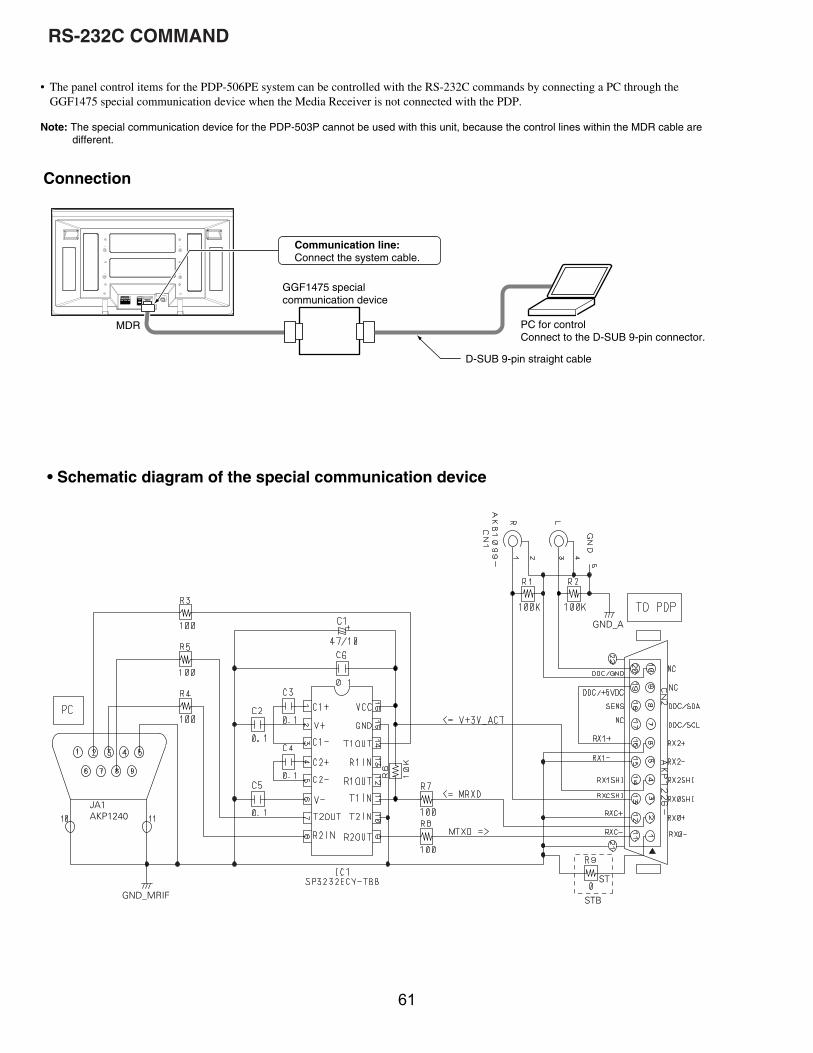
RS-232C COMMAND
SYSTEM CABLE
WHITE
BLACK
MDR
• The panel control items for the PDP-506PE system can be controlled with the RS-232C commands by connecting a PC through the GGF1475 special communication device when the Media Receiver is not connected with the PDP.
Note: The special communication device for the PDP-503P cannot be used with this unit, because the control lines within the MDR cable are different.
GGF1475 special communication device
D-SUB 9-pin straight cable
PC for controlConnect to the D-SUB 9-pin connector.
Communication line: Connect the system cable.
Connection
• Schematic diagram of the special communication device
61