Embed Size (px)
Citation preview

0
TThhee WWIINN CCaammbbrriiddggee WWoorrkksshhoopp 22001166
DDeeppaarrttmmeenntt ooff EElleeccttrriiccaall EEnnggiinneeeerriinngg
UUnniivveerrssiittyy ooff CCaammbbrriiddggee
99 JJJJ TThhoommssoonn AAvveennuuee,, CCaammbbrriiddggee,, CCBB33 00FFAA
44--55tthh JJuullyy 22001166

1
Contents
Workshop ̶ ̶ ̶ ̶ ̶ ̶ 2 Program
Participants University of Cambridge ̶ ̶ ̶ ̶ ̶ ̶ 4 University of Waterloo ̶ ̶ ̶ ̶ ̶ ̶ 15
Map & Directions ̶ ̶ ̶ ̶ ̶ ̶ 28 (with emergency contacts)

2
Workshop Program 2016
Monday, 4th July 2016
Time Topic Speaker
All Technical Presentations: 30 minutes including Q&A
9:00AM Arrivals
9:30-09:45 Welcome remarks: Professor Sir Mark Welland
9:45-10:15 Introductions: Dr.Arthur J Carty, Executive Director WIN
Start of Technical Sessions
Technical Session I: Sensors, Devices, and Imaging Technology
10:15-10:45 Manufacturing Semiconducting Tunnel Devices Dr Michael Kelly (UC)
10:45-11:15 Observing dynamics with atomic spatiotemporal resolution
Dr Germán Sciaini (WIN)
11:15-11:45 Morning Break
11:45-12:15
Transparent Semiconducting Oxides for Multifunctional Electronics : quantitative insights through semiconductor and device physics
Dr Sungsik Lee (UC)
12:15-12:45
Impurities in advanced nano-materials and theoretical and experimental approaches to miniaturization and to use of nanotechnologies for environmental and (potentially) healthcare applications
Dr Vassili Karanassios (WIN)
12:45-13:45 Lunch
Technical Session II: Printable Electronics and Flexible Display Technologies
13:45-14:15 Technologies for Nano-IT Convergence Professor Jong Min Kim (UC)
14:15-14:45
Organic Light Emitting Devices: Challenges and Research Opportunities
Dr Hany Aziz (WIN)
14:45-15:15 Functional inks of 2D materials Dr Tawfique Hasan (UC)
15:15-15:45 Afternoon Break
Technical Session II: Printable Electronics and Flexible Display Technologies (continued)
15:45-16:15
Heterogeneous integration: considerations for flexible electronics from thin-film to nano-scale devices
Dr William Wong (WIN)
16:15-16:45
Large-Area Electronics for wearable and implantable smart systems
Dr Luigi Occhipinti (UC)
16:45-17:15
Development and application of polymer semiconductors for flexible and printable electronics
Dr Yuning Li (WIN)

3
Tuesday, 5th July 2016
Time Topic Speaker
9:00AM Arrival
Technical Session III: Materials Design for Energy Harvesting and Storage
09:30-10:00
Powering the Internet of Things: Designing alternative form factors for Energy Storage Devices
Dr Pritesh Hiralal (UC)
10:00-10:30
Advanced High Energy Lithium-ion Batteries and Zinc-air Batteries
Dr Zhongwei Chen (WIN)
10:30-11:00
Nanogenerators – Small Power, Big Impact
Dr Sohini Kar-Narayan (UC)
11:00-11:30 Morning Break
Technical Session III: Materials Design for Energy Harvesting and Storage (continued)
11:30-12:00 Integrated manufacturing of nanomaterials Dr Stephan Hofmann (UC)
12:00-12:30
Controlling the assembly of exfoliated 2D nanomaterials: From blocking layers to high surface area electrodes
Dr Michael Pope (WIN)
12:30-13:00
Graphene & Carbon Nanotube-based Field Emission Devices
Dr Matthew T Cole (UC)
13:00-14:00 Lunch
Technical Session IV: Advanced Nanomaterials Technology
14:00-14:30 Catalytic DNA and Nanoparticles Dr Juewen Liu (WIN)
14:30-15:00
Semiconductor nanowires: from growth to device applications
Dr Hannah Joyce (UC)
15:00-15:30
Quantum Materials in the Two-Dimensional Limit
Dr Adam Wei Tsen (WIN)
15:30-16:00
Carbon Nanotube Transport and Exciton- Polariton Condensation
Dr Na Young Kim (WIN)
16:00 End of Workshop
19:00
Reception and Gala Dinner : Senior Combination Room (SCR) St Catharine’s College, Trumpington Street, Cambridge, CB2 1RL
Links to the venues: Meeting:
Seminar Room, Department of Electrical Engineering
University of Cambridge
9JJ Thomson Avenue, Cambridge CB3 0FA
(http://map.cam.ac.uk/West+Cambridge+Site#52.210484,0.087190,16)
Dinner:
St Catharine’s College Trumpington Street, Cambridge, CB2 1RL
Senior Combination Room (SCR). (http://www.caths.cam.ac.uk/about-us/visiting-college/maps)
4
Participants
▲Electrical Engineering Division
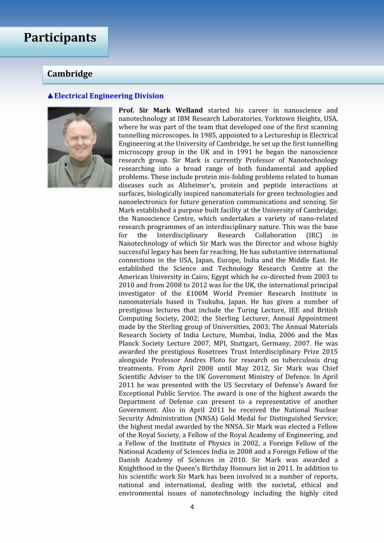
Prof. Sir Mark Welland started his career in nanoscience and nanotechnology at IBM Research Laboratories, Yorktown Heights, USA, where he was part of the team that developed one of the first scanning tunnelling microscopes. In 1985, appointed to a Lectureship in Electrical Engineering at the University of Cambridge, he set up the first tunnelling microscopy group in the UK and in 1991 he began the nanoscience research group. Sir Mark is currently Professor of Nanotechnology researching into a broad range of both fundamental and applied problems. These include protein mis-folding problems related to human diseases such as Alzheimer’s, protein and peptide interactions at surfaces, biologically inspired nanomaterials for green technologies and nanoelectronics for future generation communications and sensing. Sir Mark established a purpose built facility at the University of Cambridge, the Nanoscience Centre, which undertakes a variety of nano-related research programmes of an interdisciplinary nature. This was the base for the Interdisciplinary Research Collaboration (IRC) in Nanotechnology of which Sir Mark was the Director and whose highly successful legacy has been far reaching. He has substantive international connections in the USA, Japan, Europe, India and the Middle East. He established the Science and Technology Research Centre at the American University in Cairo, Egypt which he co-directed from 2003 to 2010 and from 2008 to 2012 was for the UK, the international principal investigator of the £100M World Premier Research Institute in nanomaterials based in Tsukuba, Japan. He has given a number of prestigious lectures that include the Turing Lecture, IEE and British Computing Society, 2002; the Sterling Lecturer, Annual Appointment made by the Sterling group of Universities, 2003; The Annual Materials Research Society of India Lecture, Mumbai, India, 2006 and the Max Planck Society Lecture 2007, MPI, Stuttgart, Germany, 2007. He was awarded the prestigious Rosetrees Trust Interdisciplinary Prize 2015 alongside Professor Andres Floto for research on tuberculosis drug treatments. From April 2008 until May 2012, Sir Mark was Chief Scientific Adviser to the UK Government Ministry of Defence. In April 2011 he was presented with the US Secretary of Defense's Award for Exceptional Public Service. The award is one of the highest awards the Department of Defense can present to a representative of another Government. Also in April 2011 he received the National Nuclear Security Administration (NNSA) Gold Medal for Distinguished Service; the highest medal awarded by the NNSA. Sir Mark was elected a Fellow of the Royal Society, a Fellow of the Royal Academy of Engineering, and a Fellow of the Institute of Physics in 2002, a Foreign Fellow of the National Academy of Sciences India in 2008 and a Foreign Fellow of the Danish Academy of Sciences in 2010. Sir Mark was awarded a Knighthood in the Queen's Birthday Honours list in 2011. In addition to his scientific work Sir Mark has been involved in a number of reports, national and international, dealing with the societal, ethical and environmental issues of nanotechnology including the highly cited
Cambridge

5
Royal Society and Royal Academy of Engineering report: “Nanoscience and nanotechnologies: opportunities and uncertainties,” that reported to the UK Government in July 2004. He has taken part in many television and radio programmes for the BBC, SKY, Open University and University of the Air, Japan and written articles for the Guardian, FT and The Times in the UK. As part of a long-term commitment to engaging with schools across Europe Sir Mark helped to design a short DVD film (narrated by Stephen Fry and translated into 12 languages) that won the Science Short Film of the Year at Scinema 2010 and is one of the most popular University of Cambridge videos (over 300,000 hits).
Prof. Arokia Nathan holds the Chair of Photonic Systems and Displays in the Department of Engineering, Cambridge University. He received his PhD in Electrical Engineering from the University of Alberta. Following post-doctoral years at LSI Logic Corp., USA and ETH Zurich, Switzerland, he joined the University of Waterloo where he held the DALSA/NSERC Industrial Research Chair in sensor technology and subsequently the Canada Research Chair in nano-scale flexible circuits. He was a recipient of the 2001 NSERC E.W.R. Steacie Fellowship. In 2006, he moved to the UK to take up the Sumitomo Chair of Nanotechnology at the London Centre for Nanotechnology, University College London, where he received the Royal Society Wolfson Research Merit Award. He has held Visiting Professor appointments at the Physical Electronics Laboratory, ETH Zürich and the Engineering Department, Cambridge University, UK. He has published over 500 papers in the field of sensor technology and CAD, and thin film transistor electronics, and is a co-author of four books. He has over 50 patents filed/awarded and has founded/co-founded four spin-off companies. He serves on technical committees and editorial boards in various capacities. He is a Chartered Engineer (UK), Fellow of the Institution of Engineering and Technology (UK), Fellow of IEEE (USA), and an IEEE/EDS Distinguished Lecturer.
Bill Milne FREng. FIET,FIMMM was Head of Electrical Engineering at Cambridge University from 1999 -2014 and was Director of the Centre for Advanced Photonics and Electronics (CAPE) from 2003-2015. In 1996 he was appointed to the ‘‘1944 Chair in Electrical Engineering’’. He obtained his BSc from St Andrews University in Scotland in 1970 and then went on to read for a PhD in Electronic Materials at Imperial College London. He was awarded his PhD and DIC in 1973 and, in 2003, a D.Eng (Honoris Causa) from University of Waterloo, Canada. He was elected a Fellow of The Royal Academy of Engineering in 2006 and awarded the J.J. Thomson medal from the IET in 2008 and the NANOSMAT prize in 2010 for excellence in nanotechnology. His research interests include large area Si and carbon based electronics, graphene, carbon nanotubes and thin film materials. Most recently he has been investigating MEMS, SAW and FBAR devices and SOI based

6
micro heaters for (bio) sensing applications. He has published/presented ~ 850 papers in these areas, of which ~ 200 were invited. He has an “h” index of 60 according to Web of Science. In 2006 he co-founded Cambridge Nanoinstruments with 3 colleagues from the Department and this was bought out by Aixtron in 2008 and in 2008 co-founded Cambridge CMOS Sensors with Julian Gardner from Warwick Univ. and Florin Udrea from Cambridge Univ. This was recently acquired by AMS, Austria. More recently, in 2013, he co-founded Cambridge X-ray Systems with Richard Parmee, Jonathan Cameron and Matt Cole.
Professor Jong Min Kim was formerly Senior Vice President and Vice President in Samsung Electronics Corporate R&D Centre, Korea for 13 years. Now, he is Professor of Electrical Engineering of Department of Engineering at University of Cambridge. He was Chair of Electrical Engineering at University of Oxford from 2012-2015. Professor Kim had previously held a variety of senior technology positions at the Samsung Group including Display, Materials, Energy and Electronics research/developments. Professor Kim had managed several tens of millions of dollars per annum for major projects in Samsung for 17 years. His research is described in more than 300 journal papers (including 8 Nature/Science, and Nature family journals), 250 publications on the Technical Digest and proceedings with around 100 keynote/invited speech at major international conference, and 253 patents (153 international patents). He received a number of awards: Best Paper Award, the Gold Prize Award by Samsung Group Chair, Prime Minister Awards (2001), Awards by Minister of Science (2000), and recently Awards by Minister of Knowledge/Economy (2012) from the Korean government. He was responsible for a number of world first inventions: carbon nanotube (reported variously in Science, Nature, etc. One paper is with more than 1,000 citation); transparent and flexible graphene electrodes (Nature 2009, with more than 3,000 citations) and quantum dot based LEDs and displays (Nature Photonics, Cover Article, 2009 and 2011, Nature Comm’13), LED on glass (Nature Photonics, Cover Article, 2011), CNT network Transistors ( Science 2008 and Nature Communications 2011), and many others. Amongst his professional achievements Professor Kim was Chair, Samsung Group Technology Conference (>1,000 papers, 2004-06, 2010-11); Member, Evaluation Committee for R&D Centres of Seoul National University (2008-9); Int. Advisory Board Member, Rus Nano Prize in Russia (2007-present), and technical committee of IEEE Int. Conference (IVNC, MTT), LOPE-C, ICFPE, etc. He had managed many high technology trans-national projects including the EU project-Takoff (FP 6 project-IST2000-28519, €10.5 m), 8 million dollars project on Creative Research by Korean Government, and more outside of Samsung: Stanford University (2003-2011), Dupont R&D Centre (2001-2006), 3M R&D Centre (2004-2010), Toray (2004-2011), Russian Academy of Science( 1995~2011), the Chinese Academy of Sciences (2003-2010) and many academia. He has been leading EC ERC Advanced Grant since 2014 and many other projects.
He had organised his selected publications in three groups. 1.Quantum Dots and Nano Materials for display/lighting, image sensors His work on Quantum Dot materials and devices began in around 2002

7
when he turned the research subject from development of CL and/or PL phosphors to research on EL devices and various convergence technologies related to solar cells and batteries. Based on nano-phosphor technology, he had found various new QD materials, structures and devices. 2. Nano Carbon and Electronics for flexible electrode, TFT, photonics, and sensors His interests in nano carbon such as CNTs and Graphene and their applications go back to 1998. As an ideal electron emitter, CNTs have been studied at the early stage of my nanocarbon related work from 1998 to 2004 then he had published more than 100 papers on nanocarbons and their applications. Nano carbon has been one of key subjects over his research career and it is still one of major focus of his group’s work. 3. Display, New Energy, and Medical Imaging System Display is one of another research bases. From early 1990’s, he had developed a number of display devices and systems such as FED, LCD, Laser TV, 3D TV, LED, PDP, OLEDs, flexible displays. He also had initiated various energy devices such as LIB, flexible battery and various types of solar cells (OPV, CIGS, DSSC and quantum dot PVs) at Samsung Electronics and it has been the framework of display and energy business of Samsung. He also has been leading research on the multi dose X-ray, and Tera Herz imaging system for future Samsung business, as well.
Talk Title Technologies for Nano-IT Convergence
Sungsik Lee received the PhD from University College London (UCL) in August 2013. He is currently working as a research associate at Cambridge University. During his PhD, he intensively investigated on device physics (e.g. carrier transport and instability mechanisms) and compact modeling of transparent semiconducting oxide-based thin film transistors (TFTs) for transparent electronic applications including optical sensors and interactive displays. His research has also enabled a design and simulation of fully TFT-based circuits and systems in a CAD environment. Previously, he worked at the Korean national lab - ETRI, where he developed a CMOS-based high performance readout integrated circuit (ROIC) for a capacitive touch sensor, which was sold in 2011. So far, he has published over 60 articles including invited/contributed journal papers, talks at flagship conferences (e.g. 2 IEDMs, SID), and 6 US patents (all awarded). Dr. Lee won the prestigious IEEE EDS PhD Fellowship and the ABTA Doctoral Researcher Award in 2011 and 2013, respectively. He won both overseas research scholarship and graduate research scholarship from UCL for his PhD study. Regarding his professional activities, he has been being a member and referee of IEEE EDS and AIP, and a guest editor of IEEE Journal of Display Technology.
Talk Title Transparent Semiconducting Oxides for Multifunctional Electronics : quantitative insights through semiconductor and device physics

8
Abstract In this talk, a transparent semiconducting oxide technology, which becomes one of the promising candidates for futuristic electronic applications besides displays, is discussed for its multi-functionality deduced from quantitative analysis through semiconductor and device physics, where its intrinsic functionality, associated with its unique material properties, as well as a macroscopic functionality, given with functional circuits, such as analog and digital circuitries to be designed and integrated in its thin film transistors, are mainly addressed in physical device modelling and relevant experimental investigations."
Research Interests - Advanced Semiconductors, e.g transparent oxides, 2-D materials - Computational analysis and modeling for electron devices. - Verilog-A coding for circuit and system design in CAD environments - Multifunctional systems with multifunctional materials.
Dr Matt Cole is an Oppenheimer Research Fellow investigating the heterogeneous integration of chemical vapour deposited aligned nanomaterials in nanoscale vacuum electronics devices. He is a Director of Cambridge Xray Systems, a spin out developing nanoengineered field emission Xray source. He is a member of the Founders of the Future Foruum and a named Forbes 30 under 30 (2016). His awards include the Sir MacFarlane Medal from the Royal Academy of Engineering, and the Silver Medal from the Institue of Materials, Minerals, and Mining, and the Sir Royce Medal from the Institute of Engineering and Technology. Dr Cole is a Fellow, College Teaching Officer, Admissions Tutor, and Director of Studies in Engineering at St Edmund's College, Cambridge University.
Talk Title Graphene & Carbon Nanotube-based Field Emission Devices
Abstract Electron emission is a ubiquitous technology. Found in travelling wave tubes, electron beam lithography systems, microwave amplifiers, thin film displays, advanced lighting units, and X-ray sources; the field of nano-vacuum electronics is returning to the fore during the present carbon renaissance. The graphitic nano-carbons out-perform conventional metallic Spindt-like electron emitters across virtually all standardised metrics. Carbon nanotubes (CNT) and graphene offer high-aspect ratios, chemical inertness, near instantaneous temporal response, with low sputter cross-sections; all of which contribute to their use as a unique platform for enhanced electron emitters. Their low turn-on fields, negligible hysteresis, and high temporal stability have resulted in significant strides towards new electron emission platforms and devices. Nevertheless, the efficient use of these emerging nanomaterials in various electron emission applications has yet to gain any significant commercial traction, largely due to temporal instabilities and challenges associated with yield and device-to-device reproducibility. Indeed, the devices that have successfully achieved high technology-readiness levels are based on poorly functioning, coarsely deposited, post-growth techniques with little to no spatial registration or controlled material alignment, using techniques often based on simplistic and material-damaging wet chemistry. Enhanced functionality, including resistance toward electromigration and beam

9
shaping, requires the ability to define, with high fidelity and reproducibility, sub-micron-scale periodic features. Here I will present our continuing, and largely pragmatic work on the development of nano-carbon based electron guns including details on the growth, characterisation and integration of chemical vapour deposited carbon nanotubes and graphene towards realising nanoscale fin electron sources, low-cost electron emitters on catalytically activated metal mesh, silicon-on-insulator ballasted CNT arrays, high electron transparent graphene triodes, and the first large-area graphene-based electron emission display.
Research Interests Carbon nanotubes, graphene, chemical vapour deposition, aligned growth, field electron emission, X-ray sources, transparent flexible electronics, nanoscale vacuum electronics (http://www3.eng.cam.ac.uk/~mtc35/index.html)
Dr Stephan Hofmann is a Reader in Nanotechnology at the Engineering Department at Cambridge University and is an internationally leading expert with 15 years of experience in the growth and device integration of nanomaterials, in particular the chemical vapour deposition (CVD) of carbon nanotubes, semiconductor nanowires and 2D materials such as graphene and hexagonal boron nitride. He leads a large EPSRC programme grant and industry consortium on CVD enabled Graphene Technology and Devices (GRAPHTED, EP/K016636/1) and is the recipient of an ERC Starting Independent Researcher Grant (InSituNANO, 279342) which focuses on novel in-situ metrology. He also is co-director of the EPSRC Centre for Doctoral Training in Sustainable and Functional Nano at Cambridge (EP/L015978/1). Among his numerous awards is the 2014 ACS Journal of Physical Chemistry C Lectureship for his outstanding contributions to the understanding of the growth and device integration of novel nanomaterials.
Talk Title Integrated manufacturing of nanomaterials
Abstract The commercial potential of nanomaterials hinges on the development of growth and integration techniques that are scalable and allow an adequate level of structural control. With a focus on diverse applications in the electronics and display industry, we aim at developing integrated process technology for nanomaterials, like 2D materials, carbon nanotubes and semiconducting nanowires. In order to go beyond empirical process calibrations, we systematically use in-situ metrology to reveal the mechanisms that govern the growth, interfaces and device behaviour of these nanomaterials in realistic process environments. The talk will focus on chemical vapor deposition (CVD), which now dominates the carbon nanotube market and rapid progress is being made to develop it also for the manufacture of graphene and other 2D materials.

10
Dr Tawfique Hasan is a University Lecturer in Electronic Materials and Devices at the Cambridge Graphene Centre, Engineering Department. He is also a Title A Fellow and a Director of Studies in Engineering in Churchill College. Dr Hasan has held several research positions in the University since his PhD, including a Junior Research Fellowship in King's College, Cambridge, a National Natural Science Foundation of China (NSFC) Foreign Young Scientist Research Fellowship and a Royal Academy of Engineering (RAEng) Research Fellowship. Dr Hasan’s current research focuses on formulation of functional 1- and 2-dimensional nanomaterial and hybrid material ink systems for low-cost, printable and flexible photonic, (opto) electronic, sensing, energy and interactive touch surface applications. He is an Associate Editor of ‘Electronics Letters’ and the new Springer-Nature journal ‘Graphene Technology’. He has published >70 articles with >8,200 citations and an h-index of 30. Research group: Hybrid Nanomaterials Engineering web: http://www-g.eng.cam.ac.uk/hasan/ twitter: @hnecam
Talk Title Functional inks of 2D materials
Abstract One of the key focus areas of my group at the Cambridge Graphene Centre is the formulation of 2D materials ink systems and their applications in photonics and electronics. I will introduce their composites and inks for ultrafast lasers in the first half of my talk. In the second half of my talk, I will discuss on applications of conductive graphene inks, including CMOS integrated inkjet printed humidity sensors, hybrid nanomaterial transparent conductors and high speed printable graphene flexo-ink systems.
Research Interests 2d materials, metal oxides, functional inks, inkjet-, flexo-, screen-printing, ultrafast lasers, batteries, large area electronics, printed touch sensors.

11
Since April 2014 Dr. Luigi G. Occhipinti holds a position at the University of Cambridge, Electrical Engineering Division, as National Outreach Manager of the EPSRC Centre for Innovative Manufacturing in Large-Area Electronics (www.largeareaelectronics.org). He is also Founder and Director of Engineering at CITC Ltd (www.citc-ltd.co.uk), a start-up company built to innovate the healthcare and medical sector. Prior to that, Luigi was R&D Programs Director and Senior Group Manager at STMicroelectronics (www.st.com), leading research teams and new business development based on Heterogeneous Integrated Smart Systems, Flexible and Disposable Electronics and New Sensors technologies. He has an Electronic Engineering degree and a PhD in Electrical Engineering. Authored and co-authored over 90 scientific publications, 2 book chapters and 37 patent families (Google Scholar H-index =18, citations 1100). Member of 2 IEEE and 3 IEC standardization committees and co-editor of the series “Cambridge Elements of Flexible and Large-Area Electronics”, by Cambridge University Press.
Talk Title Large-Area Electronics for wearable and implantable smart systems
Abstract This contribution will give an overview of state of the art Large-Area Electronics (LAE) technologies, with focus on manufacturing aspects of printed, flexible and organic electronics. Research highlights include recent and past achievements in printed sensors, hybrid integration of thinned and ultrathinned dice on flexible foils, RF energy harvesting, and emerging technologies for bio-electronics.
Research Interests Printed sensors, bio-Electronics, Large-Area Electronics
Dr Sohini Kar-Narayan is a University Lecturer (Assistant Professor) in the Department of Materials Science, leading an interdisciplinary research group in the field of energy harvesting materials and technologies. She is the recipient of a Royal Society Dorothy Hodgkin Fellowship (2011) and an ERC Starting Grant (2014), and was recognised by the World Economic Forum through a Young Scientist award (2015). She received a BSc in Physics (Honours) in 2001 from the University of Calcutta, India, and MS (2004) and PhD (2009) in Physics from the Indian Institute of Science, Bangalore. She has been a Fellow of Clare Hall College, Cambridge since 2009, and a Bye-Fellow and Director of Studies at Homerton College, Cambridge since 2014.
Talk Title Nanogenerators – Small Power, Big Impact
Abstract Harvesting energy from ambient sources in our environment has generated tremendous interest as it offers a fundamental energy solution for ‘small power’ applications, including, but not limited to, ubiquitous wireless sensor nodes; portable, flexible and wearable electronics; biomedical implants and structural/environmental monitoring devices. Energy harvesting from ambient vibrations is particularly attractive as these are ever present and easily accessible, originating from sources such as moving parts of machines, fluid flow and even body movements. In this context, piezoelectric materials offer the simplest means of directly converting mechanical vibrations into

12
electrical power and are well suited for microscale device applications, thus offering a means of superseding traditional power sources such as batteries that require constant replacing/recharging and that do not scale easily with size. In particular, nanoscale piezoelectric energy harvesters, or nanogenerators, are capable of converting small ambient vibrations into electrical energy, thus paving the way for the realisation of the next generation of self-powered devices. A recent review article from our group [1] highlighted the fact that nanogenerator research to date has mainly focused on traditional piezoelectric materials in the form of ceramics, but these are stiff and prone to mechanical failure. On the other hand, piezoelectric polymers [1-3], although less well studied, have several advantages over ceramics such as being flexible, robust, lightweight, easy and cheap to fabricate, lead free and bio compatible. However, they do suffer from inferior piezoelectric properties in comparison to ceramics. The field thus faces orthogonal difficulties associated with these two classes of materials. In order to move forward, our group aims to develop novel hybrid polymer-ceramic nanocomposites combining the best of both materials, while developing scalable nanofabrication techniques for flexible, low-cost and highly efficient polymer-based nanogenerators and sensors. [1] S. Crossley, R.A. Whiter & S. Kar-Narayan, Materials Science and Technology 30, 1613 (2014). [2] R.A. Whiter, V. Narayan & S. Kar-Narayan, Advanced Energy Materials DOI: 10.1002/aenm.201400519 (2014) [3] S. Crossley & S. Kar-Narayan, Nanotechnology 26, 344001 (2015).
Research Interests Functional nanomaterials for energy applications, with particular focus on piezoelectric, ferroelectric and thermoelectric materials and devices for energy harvesting, sensing and cooling applications.
Michael Kelly has been the Prince Philip Professor of Technology at Cambridge since 2002. Before that he was head of Electronic Engineering at Surrey and in the 1980s he worked at the GEC Hirst Research Centre on multilayer semiconductor devices. His interests are in (i) manufacturable tunnel devices and (ii) manufacturability at the nanoscale. He is a Fellow of the Royal Society of London and of New Zealand and of the Royal Academy of Engineering.
Talk Title Manufacturing Semiconducting Tunnel Devices
Abstract I demonstrate recent progress on the achievement of high uniformity within a wafer and high reproducibility between wafers of the DC and RF performance of microwave detector diodes that relies for its operation on quantum mechanical tunnelling through a 10-monolayer thick barrier of AlAs in GaAs
Research Interests Semiconductor multilayers – material, physics, technology, devices

13
Dr Hannah Joyce completed her PhD at the Australian National University in 2009 under the supervision of Prof. C. Jagadish and Prof. Hoe Tan. After her PhD, she joined the Department of Physics, University of Oxford, as a postdoctoral research fellow. In 2013 she was awarded a research fellowship from the Royal Commission for the Exhibition of 1851, and joined the University of Cambridge as a university lecturer. Her primary research interest is the development of semiconductor nanostructures as nano-components in novel nanoelectronic and nanophotonic devices, for future use in electronics, solar energy, communication systems and medicine.
Talk Title Semiconductor nanowires: from growth to device applications
Abstract III–V semiconductor nanowires exhibit outstanding potential as nano-building blocks for the next generation of electronic devices, ranging from solar cells to nanoscale lasers. We use a variety of fabrication techniques to grow these nanowires with tight control over the nanowire geometry and crystallographic properties. Electrical characterisation of these nanowires can be achieved with high accuracy and high throughput without requiring any electrical contacts, using terahertz conductivity spectroscopy. This talk will discuss how detailed nanowire growth studies together with terahertz conductivity spectroscopy are guiding the development of novel nanowire-based devices.
Research Interests Nanowire growth, metalorganic vapour phase epitaxy, molecular beam epitaxy, terahertz spectroscopy, photoluminescence spectroscopy, photovoltaics, light emitting diodes.
Dr. Pritesh Hiralal received the MPhys (Hons) degree in Physics from the University of Manchester, UK, in 2003. After spending time in business in Spain, and setting up Zendal Backup, he went on to complete a Ph.D. from the Department of Engineering at Cambridge University. He has spent time in industry at the Nokia Research Centre working on high power energy storage where he holds several patents under his name. He has been Research Associate as well as an adjunct lecturer at the University of Cambridge, with research interests including the understanding of the growth of nanomaterials and the combination of these into different architectures for photovoltaics and energy storage devices including batteries and supercapacitors. He has now founded Zinergy, to develop and commercialise printed battery technology.
Talk Title Powering the Internet of Things: Designing alternative form factors for Energy Storage Devices

14
Abstract The advent of the Internet of Things brings about many interesting possibilities. The ubiquitous placement of sensors is able to provide a wealth of data that can be used to enhance our daily lives. However, the issue of powering these devices still remains; the batteries or capacitors used are the bulkiest part of the device and often provide limited lifetimes. A shift from the traditional coin cell or can structures would provide the flexibility required to design truly embedded and independent sensors. I will summarise a vision of research around designing energy storage devices of different form factors, and look into a little more detail into two examples: flexible/stretchable devices suitable for printed electronics or wearable applications and microchip embedded energy storage suitable for on-chip applications such as sensors. In order to accomplish this, a combination of tailoring material properties and device structure is required. For instance, microsupercapacitors and microbatteries have gained particular interest as potential integrated power sources for microelectromechanical systesms (MEMS). These devices typically consist of patterned interdigitated electrodes which remove the necessity for the use of electronically insulating separators. However, many integration challenges exist. Further, given the limited physical space available in microdevices, it is of utmost importance to maximise the power/energy density attainable per area. Ideas for research include both the materials aspect (e.g. high density electrode growth) as well architecture (e.g. using fractal patterns to increase power density). Illustrative examples will be provided around carbon, which, with its numerous forms and allotropes, is a very versatile material, and has been used in batteries and capacitors for a number of functions, including current collection, conductive additive and ion intercalation material. I will explain how it is possible to tailor the morphology of carbon for instance to adapt its mechanical (e.g. flexibility) and electrical (e.g. low resistance) properties to the required function, and ultimately achieve the required objectives.
Research Interests Energy storage, batteries, supercapacitors, nanomaterials, photovoltaics

15
▲University of Waterloo
Dr. Arthur Carty is the Executive Director of the Waterloo Institute for Nanotechnology at the University of Waterloo, Special Advisor to the President on international science and technology collaboration and Research Professor in the Department of Chemistry. From 2004-2008, he served as Canada’s first National Science Advisor to the Prime Minister and to the Government of Canada. Prior to his appointment as National Science Advisor, he was President of the National Research Council Canada (NRC), Canada’s National Laboratory, for ten years (1994-2004). Dr. Carty has a PhD in inorganic chemistry from the University of Nottingham. Before joining NRC in 1994, he spent two years at Memorial University and then 27 years at the University of Waterloo where he was successively Professor of Chemistry, Director of the Guelph-Waterloo Centre for Graduate Work in Chemistry, a pioneering joint graduate program, Chair of the Department of Chemistry for two terms and Dean of Research. Dr. Carty still maintains an active interest in research in organometallic chemistry and new materials. He has 318 publications in peer reviewed journals, 9025 citations to his work and five patents to his credit. He is a former President of the Canadian Society for Chemistry, an honorary fellow of the Chemical Institute of Canada, a Fellow of the Fields Institute for Research in the Mathematical Sciences, a Fellow of the Royal Society of Canada and a Fellow of the American Association for the Advancement of Science. Amongst his many awards are the Alcan Award and the Montreal Medal of the Chemical Institute of Canada, the E.W.R. Steacie Award of the Canadian Society of Chemistry, the Purvis Award of the Society of Chemical Industry, the Queen Elizabeth II Golden Jubilee (2002) and Diamond Jubilee (2012) Medals and the Taiwan National Science Council Professional Medal. He has been accorded 14 honorary degrees from foreign and Canadian universities as well as honorary professorships at three other institutions outside Canada. Dr. Carty has received Canada’s highest civilian award as an Officer of the Order of Canada (OC) and has also been honoured by France as Officier de l’Ordre National du Mérite. He is Honorary Dean of the College of Nano Science and Technology at Soochow University, China. He has served as chair/member of many Boards of Directors including the Atomic Energy Control Board (AECB) and its successor Canadian Nuclear Safety Commission (CNSC), the Council of the Canadian Space Agency, the Boards of Genome Canada, of MITACs and the Stroke Network, both Networks of Centre of Excellence (NCE) and of Environment Canada and National Defence's Research & Development Advisory Board. He was the founding Chairman of the Board of the Canadian Light Source (CLS), serving from 1999 to 2008. He is a member of the Council of Japan’s Science and Technology in Society Forum (STS) and has served on the International Advisory Boards of the Asia-Pacific Economic Cooperation (APEC) Centre for Technology Foresight and the Euroscience Open Forum (ESOF). Dr. Carty currently serves on the Boards of Directors of Ecosynthetix Inc. Dr. Carty was inaugural Canadian co-Chair of the Joint Science and Technology Cooperation Committee for the Canada-India science and technology agreement and has contributed to the growth of R&D collaboration

16
between the two countries. As National Science Advisor, he also represented Canada from 2004-2008 on behalf of the minister at the semi-annual Carnegie Group G-8 meetings of science ministers and science advisors. In September 2008, Dr. Carty was appointed as a Science Advisor to the Premier of Taiwan and Member of the Board of Taiwan’s Executive Yuan Science and Technology Advisory Group (STAG). He has also served as a member of the Advisory Board of the National Science Council (Taiwan).
Dr Lisa Pokrajac is a UW graduate, first earning her BSc at UW in Honour’s Applied Chemistry, Co-operative Program, and then completing her MSc at the University of Toronto in surface analysis. She returned to Waterloo for doctoral studies, investigating the oligomerization properties of the cholesterol-dependent toxin, pyolysin. As Assistant Director of Research Programs at WIN, Lisa provides high-level coordination and management of WIN’s scientific and engineering programs. These include academic and corporate partnerships, international collaborations, faculty awards, and outreach programs. She is also responsible for technical writing and communications for WIN, including marketing and funding applications. Lisa has a strong interest in education, and holds a Certificate of University Teaching from UW’s Centre for Teaching Excellence.
Hany Aziz is a Professor in the Department of Electrical & Computer Engineering, University of Waterloo and the Waterloo Institute for Nanotechnology, and is the Associate Director of the Nanotechnology Engineering program. He conducts research in the area of organic electronic and optoelectronic materials and devices, with a focus on material and device physics. He has published more than 130 research papers in this area and was awarded 53 US patents. In the period 2009-2013 he held the appointment of NSERC-DALSA Industrial Research Chair. Prior to joining the University of Waterloo in 2007, he was a research scientist at Xerox Research Centre of Canada. Hany obtained a B.Sc. in Mechanical Engineering from the American University in Cairo in 1989, and a Ph.D. in Materials Science and Engineering from McMaster University, Canada in 1999.
Talk Title Organic Light Emitting Devices: Challenges and Research Opportunities
Abstract Almost 30 years after their invention, Organic Light Emitting Devices (OLEDs) are now used in flat panel displays. As the technology moves from the lab to the market place, certain fundamental and technological issues related to OLED reliability, efficiency and manufacturing become increasingly more important and create new opportunities for research. In this talk a number of those issues will be highlighted and some of our research activities to address them will be briefly reviewed. In this context, some recent results from our investigations of degradation mechanisms in wide band-gap OLEDs, the development of novel RGB color patterning techniques for flexible OLED displays and approaches
17
for realizing high brightness quantum-dot LEDs will be presented.
Research Interests Organic optoelectronic materials and devices (OLEDs, organic solar cells, sensors)
Charge and energy transfer processes in organic optoelectronic materials
Device reliability and material aging phenomena; devide degradation mechanisms
Quantum-dot LEDs
Novel fabrication processes for flat panel displays
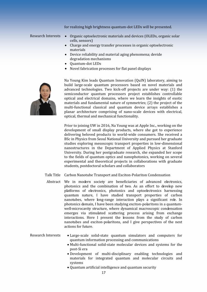
Na Young Kim leads Quantum Innovation (QuIN) laboratory, aiming to build large-scale quantum processors based on novel materials and advanced technologies. Two kick-off projects are under way: (1) the semiconductor quantum processors project establishes controllable optical and electrical domains, where we learn the insights of exotic materials and fundamental nature of symmetries; (2) the project of the multi-functional classical and quantum device arrays establishes a planar architecture comprising of nano-scale devices with electrical, optical, thermal and mechanical functionality.
Prior to joining UW in 2016, Na Young was at Apple Inc., working on the development of small display products, where she got to experience delivering beloved products to world-wide consumers. She received a BSc in Physics from Seoul National University and pursued her graduate studies exploring mesoscopic transport properties in low-dimensional nanostructures in the Department of Applied Physics at Stanford University. During her postgraduate research, she expanded her scope to the fields of quantum optics and nanophotonics, working on several experimental and theoretical projects in collaborations with graduate students, postdoctoral scholars and collaborators
Talk Title Carbon Nanotube Transport and Exciton-Polariton Condensation
Abstract We in modern society are beneficiaries of advanced electronics, photonics and the combination of two. As an effort to develop new platforms of electronics, photonics and optoelectronics harnessing quantum nature, I have studied transport properties of carbon nanotubes, where long-range interaction plays a significant role. In photonics domain, I have been studying exciton-polaritons in a quantum-well-microcavity structure, where dynamical macroscopic condensation emerges via stimulated scattering process arising from exchange interactions. Here I present the lessons from the study of carbon nanotubes and exciton-polaritons, and I give perspectives of the next actions for future.
Research Interests Large-scale solid-state quantum simulators and computers for quantum information processing and communications Multi-functional solid-state molecular devices and systems for the
post-Si era Development of multi-disciplinary enabling technologies and
materials for integrated quantum and molecular circuits and systems Quantum artificial intelligence and quantum security

18
After receiving a BS in Electrical Engineering and Computer Sciences, as well as a BS in Engineering Physics at the University of California, Berkeley, he completed his PhD in Applied Physics at Cornell University under the guidance of Jiwoong Park. Tsen then joined the Department of Physics at Columbia University as a postdoctoral associate with Abhay Pasupathy and Philip Kim, where he studied atomically thin quantum materials and incorporated them in nanoscale electronic devices. Professor Adam Wei Tsen joined the Waterloo Institute for Nanotechnology (WIN), the Institute for Quantum Computing (IQC) and the Department of Chemistry as an assistant professor in 2016. The Tsen group employs a combination of experimental techniques for materials characterization at the nanoscale (transmission electron microscopy, micro-optical spectroscopy, magnetotransport measurements, etc.) as well as state-of-the-art nanofabrication processes for device engineering.
Talk Title Quantum Materials in the Two-Dimensional Limit
Abstract The layered metallic dichalcogenides host rich quantum phases such as charge density waves, spin density waves, and superconductivity. In the past, studies on graphene and various semiconducting dichalcogenides have shown that taking layered materials to their physical two-dimensional (2D) limit leads to fundamental changes in band structure, allowing for a powerful experimental knob to tune for electronic functionality. In contrast, due to their instability in the ambient environment, the effect of thickness control over such quantum phases has been largely unexplored. We have recently demonstrated an experimental platform to isolate environmentally sensitive 2D quantum materials. I will discuss our studies of the charge density wave compound 1T-TaS2 and superconducting 2H-NbSe2 in the atomically thin limit, made possible using this technique. In TaS2, we uncover a new surface charge density wave transition that is distinct from that in the bulk layers, as well as demonstrate continuous electrical control over this phase transition. In NbSe2, a small perpendicular magnetic field induces a transition to a quantum metallic phase, the resistivity of which obeys a unique field-scaling consistent with that predicted for a Bose metal. These methods and experiments open new doors for the study of other correlated 2D systems in the immediate future.
Research Interests Low-dimensional quantum materials Novel microscopy techniques and characterization Manipulation and fabrication of mesoscopic (opto)electronic
devices

19
Juewen Liu received his BSc from the University of Science and Technology of China in 2000, and PhD in Chemistry from the University of Illinois at Urbana-Champaign in 2005. After postdoctoral research at the University of New Mexico and Sandia National Laboratories, he joined the Department of Chemistry of University of Waterloo in Canada in 2009. He is interested in the adsorption of biomolecules such as DNA and lipids by nanomaterials both for fundamental understandings and for analytical and biomedical applications. His group also develops DNA-based biosensors for environmental and biomedical analysis. He received an Early Researcher Award from the Ontario Ministry of Research and Innovation (2011) and the Fred Beamish Award from the Canadian Society for Chemistry (2014). He has authored over 150 papers, receiving nearly ten thousand citations. More information can be found in his webpage: http://www.science.uwaterloo.ca/~liujw/index.html
Talk Title Catalytic DNA and Nanoparticles
Abstract Abstract: In this talk, recent developments in my lab on catalytically active DNA (DNAzymes) and nanoparticles (nanozymes) will be discussed. DNAzymes are DNA-based catalysts and we focus on RNA-cleaving DNAzymes. Using lanthanide ions as cofactors, we isolated a suite of new DNAzymes that can selectively detect rare-earth metals. By using phosphorothioate modified DNAzymes, we developed new probes for a few toxic heavy metal ions. Biochemical characterization and analytical applications of these DNAzymes will be discussed. The adsorption of DNA by various metal oxides were studied, where the phosphate backbone of DNA is shown to be critical for the adsorption reaction. Using fluorescently labeled DNA, highly sensitive detection of arsenate and hydrogen peroxide was achieved. Finally, nanozymes activity can be adjusted by adding DNA or other molecules. Efforts in exploring the mechanistic aspects will be reported.
Research Interests Bio-inspired self-assembly and bionanotechnology DNA aptamers Targeted drug delivery/nanomedicine Bioinorganic/bioanalytical chemistry
Michael Pope is an Assistant Professor in the Department of Chemical Engineering who recently began his research program at Waterloo in September 2014. He obtained his PhD from Princeton University where he studied the production and processing of graphene-based materials into advanced batteries and supercapacitors. During his post-doctoral work at Vorbeck Materials Corp., a large-scale graphene producer, he was the technical lead on a developmental program to commercialized Li-S batteries, he built and operated a pilot-scale fiber spinning line for producing high strength graphene-filled polyesters and contributed to Vorbeck’s graphene ink development. His group focuses on developing processing strategies and nanocomposites from a variety of 2D materials and polymers for applications including energy storage, electrocatalysis, electronics, and

20
membranes separations. Concepts in interfacial engineering are used to design films and composites with improved properties and by methods amenable to scalable production and manufacturing. His prior research has resulted in 15 publications and 6 patents.
Talk Title Controlling the assembly of exfoliated 2D nanomaterials: From blocking layers to high surface area electrodes
Abstract Graphene and related 2D nanomaterials are expected to revolutionize many applications due to their unique optical, electronic and mechanical properties. These atomically thin sheets are typically micron to submicron-sized in lateral extent when exfoliated from bulk precursors and must be controllably assembled into large area films or coatings to form functional nanocomposites. Graphene-based materials hold significant promise for applications requiring electrodes with high surface area and porosity while, on the other hand, they can also be processed into non-porous, gas impermeable films. Engineering materials which traverse these seemingly conflicting abilities depend largely on how we manipulate their colloidal assembly and aggregation behavior. In this talk, I will give an overview of the research being carried out in my lab which has the general theme of creating improved materials and processing strategies to create well-defined films and nanocomposites from exfoliated 2D materials such as graphene and molybdenum disulfide. I will discuss a promising strategy we are developing to manipulate these 2D materials at the air-water interface using a modified Langmuir-Blodgett method. Using this approach we engineer well-defined monolayers and multilayers for applications in electronics, as blocking layers and selective membranes. I will also discuss our recent efforts to create improved electrode materials and processing strategies for high voltage supercapacitors as well as Li-S batteries. We investigate these energy storage systems as both traditional sandwich-type cells as well as flexible, interdigitated cells created by laser patterning.
Research Interests Directed assembly of 2D nanomaterials at the air-water interface
Bottom-up assembly approaches for energy storage, sensing and electrocatalysis
Nanocomposite anode/cathode designs for advanced batteries Metal anode protection strategies
Laser-scribed supercapacitor/batteries

21
Professor Vassili Karanassios is a faculty member in the Department of Chemistry of the University of Waterloo (UW), a member of the Waterloo Institute for Nanotechnology and a co-founder of a degree program in Nanotechnology Engineering at UW. He received his PhD degree in Chemistry from the University of Alberta (Edmonton, Alberta, Canada). After that, he was a Post Doctoral Fellow in the Department of Chemistry, McGill University (Montreal, Quebec, Canada). Since 2000, he holds the rank of Professor. For his 2009 sabbatical in the UK, he was a visiting Professor in Cambridge University (in the Center of Advanced Photonics and Electronics or CAPE, under the direction of Professor William Milne) and was also a visiting Professor in the Department of Chemistry, Sheffield University (in a chemistry laboratory under the direction of Professor Cameron McLeod). At that time, he held a Leverhulme award.
Talk Title Impurities in advanced nano-materials and theoretical and experimental approaches to miniaturization and to use of nanotechnologies for environmental and (potentially) healthcare applications
Abstract The research theme of my research group focusses on three inter-related areas:
1. In nano, it is widely accepted that “size defines properties”. But
then, so do impurities (a fact mostly neglected). For example, many
years ago, numerous early claims on the capabilities of carbon
nano-tubes where due to impurities. A unique method to
determine impurities in nano-materials (providing about 100-times
improvement in sensitivity over conventional methods will be
disused in some detail),
2. Micro- and nano-instruments for taking the lab to the sample types
of appkications. We have been working on development of
instrumentation (e.g., shoe box size, shirt pocket size and eventually
wearable) that will alter the traditional chemical analysis paradigm
(i.e., of bringing a sample to a lab), by developing instrumentation
that will allow practitioners to bring (part of) the lab to the sample.
The sample can be part of the environment (e.g., the water we
drink) or a patient.
a. We fabricated (using semiconductor fabrication technology) and
more recently 3D printed, sugar-cube size, battery-operated
microplasmas (e.g., the types of plasmas used for semiconductor
fabrication, but unlike them, they operate at atmospheric
pressure).
b. We are exploring energy scavenging and energy harvesting
approaches to make microplasma-based systems energy
autonomous
c. We are developing wireless communications approaches, so that
miniaturized instruments can acquire and process data (e.g.,
FFTs) using a smart phone.
d. We are characterizing, self-powered (i.e., an external power
source is not required), light-weight, inexpensive detectors for

22
wavelengths in the visible part pf the spectrum on flexible
substrates. The approach can be used for healthcare
applications.
e. We are examining the effect of scaling laws on miniaturized
micro- and nano-instruments.
3. Use of (functionalized) graphene oxide to selectively extract Cr
species in environmental samples (e.g., water). More specifically, Cr
in waters can exist in two oxidation states: Cr(III) and Cr(VI). But
while Cr(III) is an essential micronutrient, Cr(VI) is reported to be
carcinogenic. We developing approaches to use functionalized
graphene oxide to selectively extract either Cr(III) or Cr(VI) from
water. This is important because over 30% of deaths worldwide
are reported to be due to poor water quality.
In this, breadth rather than depth presentation, the research themes described above will be discussed in some detail.
Research Interests The vision of my research is to cause a paradigm shift in classical chemical analysis by allowing practitioners to bring the lab to the sample. This will be accomplished by using miniaturization approaches and nanoscience and nanotechnologies. Research in this area is aimed at making chemical analysis
instruments smaller, cheaper, faster and smarter via integration of chip-based, battery-operated, shoe box size (and eventually shirt-pocket size) micro- and nano-instruments that can be used for chemical analysis in the field (where analytical results are needed the most).
Selected research projects include: o Development of battery-operated photon and ion sources (e.g.,
microplasmas on chips using MEMS and 3D printing technologies)
o Development of miniaturized optical and mass spectrometers
o Development of flexible, light-weight, inexpensive, self-powering (i.e., no external power is required) detectors for the visible part of the spectrum
o Energy harvesting and energy scavenging approaches for micro- and nano-instruments (to used for unattended in the field)
o Wireless data acquisition (and signal processing) for field use
o Spectral interference correction via use of Artificial Neural Networks (ANNs)-to address interferences due to poor resolution of miniaturized spectrometers
o Development of functionalized graphene oxide sorbents for measurement of inorganic pollutants in the environment, for example, for Cr3+ (an essential micronutrient) and for Cr6+ (a carcinogen). DFT approaches will be useful.

23
Professor William S. Wong is a Professor at the University of Waterloo in the Department of Electrical and Computer Engineering. Wong received his PhD in materials science from the University of California, Berkeley in 1999. Following 10 years as senior member of research staff at the Palo Alto Research Center (formerly Xerox PARC) he joined the faculty at University of Waterloo in 2010. While at PARC, Wong’s research focused on large area electronics where he began programs in printed and flexible electronics. His current research include transition-metal oxide thin-films for flexible electronics, hybrid nanowire/thin-film radial junction solar cells, ink-jet printing of polymeric circuits for image sensor and display applications, and integrated ultraviolet light emitters in fabric for water purification.
Talk Title Heterogeneous integration: considerations for flexible electronics from thin-film to nano-scale devices
Abstract Conventional monolithic integration methods are reaching a practical limit for large-area electronics where miniaturization is not the major constraint for scaling the technology. This platform may benefit more from heterogeneous integration as a means to enhance micro- and nano-system functionality. Examples of enhanced micro-system functionality will be given using novel approaches to materials and device integration employing ink-jet printing of thin-film transistors (TFTs) to “paste-and-cut” approaches for high-brightness solid-state lighting. As a demonstration of enhancing nano-system functionality, the fabrication of flexible 3-D nanowire solar cells will be described to create self-cleaning photovoltaics. The optical and electrical characteristics of these radial-junction devices can be optimized through mechanical bending while the nanostructure surface may be manipulated to create a self-cleaning surface, maintaining a pristine exterior for the nanowire solar cell to maximize light capture. Finally, a discussion of the effect on mechanical strain on the electrical and optical characteristics of flexible electronics will be reviewed.
Research Interests Flexible and Printed Electronics Solid-state Lighting Nanofabrication for Energy Conversion and Storage Large-area electronics Laser Processing of Materials
Professor Yuning Li in the Department of Chemical Engineering is working on nanomaterials/electronic materials for organic electronic applications. Professor Li earned his BSc and MSc degrees in polymer materials design at Dalian University of Technology in China, and went on to obtain his doctorate at the Japan Institute of Science and Technology (JAIST). After graduation, Professor Li worked at the National Research Council Canada, the Xerox Research Centre of Canada (XRCC), and the Institute of Materials Research and Engineering (IMRE) in Singapore. In 2010, Professor Li joined the Department of Chemical Engineering at the University of Waterloo.
Talk Title Development and application of polymer semiconductors for flexible and printable electronics

24
Abstract Polymer semiconductors are enabling materials for a range of printed electronics including organic thin film transistors (OTFTs), organic photovoltaics (OPVs), and organic light emitting diodes (OLEDs). As channel semiconductors in OTFTs, charge carrier mobility on par with that of amorphous silicon (~0.1-1 cm2V-1s-1) or higher is required for many applications. The development of polymer semiconductors with such high mobility has been a great challenge. In the past few years we have developed more than 10 novel chemical building blocks for polymer semiconductors. These new polymers show promising optoelectronic properties and /or excellent air stability, which are suitable for logic circuits, phototransistors, chemical sensors, OPVs, and other emerging flexible/printable optoelectronics. One particular class of such polymers are based on a diketopyrrolopyrrole (DPP) acceptor building block. By carefully choosing the electron donor blocks, we have successfully developed p-type polymers with high mobility up to 6.9 cm2V-1s-1 and amibipolar polymers with balanced electron and hole mobility of 6.30 cm2V-1s-1 and 2.78 cm2V-1s-1, respectively. By using polyethylenimine (PEI) as an electrode modification layer or an n-dopant, we were able to block the hole injection or trap the injected holes and successfully transform ambipolar and even p-type transistors unipolar n-type transistors. These are rather general approaches to obtaining unipolar n-type polymer semiconductors that are highly demanded in printed CMOS logic circuits and thermoelectrics. References Li, Y.; Singh, S. P.; Sonar, P. Adv. Mater. 2010, 22, 4862.
Li, Y.; Sonar, P.; Singh, S. P.; Soh, M. S.; van Meurs, M.; Tan, J. J. Am. Chem. Soc.
2011, 133, 2198.
Sun, B.; Hong, W.; Yan, Z.; Aziz, H.; Li, Y. Adv. Mater. 2014, 26, 2636.
Sun, B.; Hong, W.; Thibau, E.; Aziz, H.; Lu, Z.H.; Li, Y. Organic Electronics
2014, 15, 3787.
Sun, B.; Hong, W.; Aziz, H.; Li, Y. ACS Appl. Mater. Inter., 2015, 7, 18662.
Deng, Y.; Sun, B.; He, Y.; Quinn, J.; Guo, C.; Li, Y. Angew. Chem. Int. Ed. Engl.,
2016, 55, 3459. Research Interests Professor Li’s research involves molecular engineering of polymer
semiconductors and low temp-process conductive inks for printed electronics with the following emphases:
1. Design and molecular engineering of organic/polymer semiconductors for organic electronics
Organic Thin Film Transistors (OTFTs) Polymer bulk-heterojunction photovoltaics (OPV) Small molecule-based OPV Dye-sensitized Solar Cells (DSSC) Organic Light-Emitting Diodes (OLEDs) Chemical/biosensors and photo-detectors
2. Low temperature-processable conductive inks Metal nanoparticle inks for printing highly conductive features
on plastic substrates Solution processable transparent conductors to replace expensive Indium-Tin-Oxide (ITO)

25
Dr. Zhongwei Chen is Canada Research Chair Professor in Advanced Materials for Clean Energy at University of Waterloo. His research interests are in the development of advanced energy materials for metal-air batteries, lithium-ion batteries and fuel cells. He has published 1 book, 7 book chapters and more than 150 peer reviewed journal articles with over 10,000 citations with H-index 45 (GoogleScholar). He is also listed as inventor on 15 US/international patents, with several licensed to companies in USA and Canada. He was recipient of the 2016 E.W.R Steacie Memorial Fellowship, which followed shortly upon several other prestigious honors, including the Ontario Early Researcher Award, an NSERC Discovery Accelerator Supplements Award, the Faculty Distinguished Performance Awards and the Research Excellence Awards from the University of Waterloo, the Finalists for the 2015 R&D 100 Awards.
Talk Title Advanced High Energy Lithium-ion Batteries and Zinc-air Batteries
Abstract Development of low cost, high energy, safe and long-life rechargeable battery technology is critical for widespread commercialization of smart grid and electric vehicle. Rechargeable lithium-ion batteries and rechargeable zinc-air batteries have been considered as most promising candidates as energy storage system for transportation, smart grids and stationary power. In this presentation, I will present our recent work on advanced energy materials development for next generation rechargeable lithium-ion batteries and rechargeable zinc-air batteries by focusing on the following two topics: (1) The latest achievements and some ongoing work in silicon anode based high energy Li-ion battery through the collaboration with General Motors. More specifically, advanced Si electrodes have been developed by a simple flash heat treatment and sulfur-doped graphene wrapping technique which can efficiently accommodate Si volume expansion and demonstrate excellent electrochemical reversibility and cycling. (2) Novel nano-engineered core-corona structured bi-functional catalysts and electrodes for rechargeable zinc-air batteries. We will also discuss how nanoengineered materials can enhance the catalytic activity and durability of oxygen electrocatalysts, how the 3-D air electrode could improve the performance of the zinc-air batteries and how the novel flow system solve the zinc dendrite problem in the zinc-air batteries.

26
Professor Germán Sciaini is a world expert in the field of ultrafast structural dynamics. He received his degree of Licentiate in Chemistry and PhD with distinction from the University of Buenos in 2001 and 2006, respectively. Since 2006, as a postdoctoral fellow at the University of Toronto and later on as a Group Leader at the Max Planck for Structure and Dynamics of Matter, Sciaini has been developing state-of-art instrumentation for the study of dynamical phenomena with prerequisite spatial (10-10 m) and temporal (10-13 s) resolutions to capture atoms in motion.
Sciaini joined the University of Waterloo as an Associate Professor in January 2014. He has co-authored more than 30 publications in total; including 1 Science report, 3 Nature reports, and 3 extensive review articles.
Sciaini is a Canada Research Chair (Tier 2) in “atomically resolved dynamics and ultrafast high-resolution imaging”, he is heading the Ultrafast electron Imaging Laboratory (UeIL), at the Department of Chemistry, which is home of a time-resolved electron diffraction setup and an ultrafast high-resolution electron microscope.
Talk Title Observing dynamics with atomic spatiotemporal resolution
Abstract The progress in the development of ultrafast structural probes during the last twenty years has been tremendous. Current ultrafast imaging techniques provide the temporal and spatial resolutions required for the stroboscopic observation of atoms in motion. With an effective brightness only one hundredfold below that of the brightest femtosecond X-ray source on earth (LCLS, Stanford), ultrabright femtosecond electron diffraction has revealed atomic level views of photo-induced reactions and phase transformations [1] to culminate with the first “molecular movie” in a labile organic system [2]. This latter study illustrates the potential of ultrashort electron bursts for capturing, with atomic resolution, the key structural changes governing chemical reactivity and biological function. I will present a brief overview of the growing field of ultrafast structural dynamics along with some recent advances done in the design of ultrafast electron guns, which will soon enable monitoring dynamical processes with sub-30 femtosecond temporal resolution [3].
[1} G. Sciaini and R. J. Dwayne Miller. “Femtosecond electron diffraction: heralding the era of atomically resolved dynamics” Rep. Prog. Phys. 74, 096101 (2011). [2] M. Gao, C. Lu, H. Jean-Ruel, L. C. Liu, A. Marx, K. Onda, S-y. Koshihara, Y. Nakano, X. Shao, T. Hiramatsu, G. Saito, H. Yamochi, R. R. Cooney, G. Moriena, G. Sciaini and R.J.D. Miller. “Mapping molecular motions leading to charge delocalization with ultrabright electrons”. Nature 496, 343 (2013). [3] A. Petruk, K. Pichugin and G. Sciaini. Shaped cathodes for the generation of sub-30 fs electron bunches. In preparation.

27
Research Interests Ultrafast lasers provided the “first light” in sufficiently short pulses to monitor atomic motion on the relevant timescales; below a millionth of a millionth of a second, to literally catch atoms on the fly as in stop-motion photography. However, the spatial resolution in optical microscopy is limited to about the size of a big virus. This is about ten thousand times too coarse to observe the molecular structure at its finest detail, down to its fundamental building blocks – atoms.
The UeIL team designs and implement ultrafast electron imaging tools and electron microscopy accessories to study nanomaterials and chemical reactions with atomic spatio-temporal resolution. The main developments in Sciaini's group involve:
Femtosecond electron diffraction for the investigation ultrafast structural dynamics. This research line brings to the lab bench experiments that otherwise require the use of large-scale hard X-ray free electron laser facilities such as LCLS (SLAC, USA) and SACLA (Spring8, Japan).
Ultrafast electron microscopy for the determination of 3D structures of labile molecular systems (i.e. organic materials and proteins).
Nanofluidics for investigation of liquid samples by in-situ high-resolution electron microscopy.

28
Maps & Directions
█ Emergency Contacts:
Ms Tara Thorneycroft (Tel. +44-7765315674 or 1223-748380)
Main Reception at Dept of Electrical Engineering (Tel: +44-1223 748300)
▲Electrical Engineering Seminar Room, CAPE, Department of Engineering, University of Cambridge 9JJ Thomson Avenue, Cambridge CB3 0FA http://map.cam.ac.uk/West+Cambridge+Site#52.210484,0.087190,16
▲Tuesday, 5th July, 7PM St Catharine’s College, The Senior Combination Room (SCR). Trumington Street, Cambridge CB2 1RL http://www.caths.cam.ac.uk/about-us/visiting-college/maps
West Cambridge Site
Dinner

29

30
WWeesstt CCaammbbrriiddggee SSiittee