Embed Size (px)
Citation preview
Tunnel conductivity switching in a singlenanoparticle-based nano floating gatememoryAlessandro Gambardella1, Mirko Prezioso2 & Massimiliano Cavallini1
1Consiglio Nazionale delle Ricerche-Istituto per lo studio dei Materiali Nanostrutturati (CNR- ISMN), via P. Gobetti 101, 40129Bologna, Italy, 2University of California, Santa Barbara Electrical & Computer Engineering Harold Frank Hall.
Nanoparticles (NPs) embedded in a conductive or insulating matrix play a key role in memristors and inflash memory devices. However, the role of proximity to the interface of isolated NPs has never been directlyobserved nor fully understood. Here we show that a reversible local switching in tunnel conductivity can beachieved by applying an appropriate voltage pulse using the tip of a scanning tunnelling microscope on NPsembedded in a TiO2 matrix. The resistive switching occurs in the TiO2 matrix in correlation to the NPs thatare in proximity of the surface and it is spatially confined to the single NP size. The tunnel conductivity isincreased by more than one order of magnitude. The results are rationalized by a model that include thecharge of NPs that work as a nano floating gate inducing local band bending that facilitates charge tunnellingand by the formation and redistribution of oxygen vacancies that concentrate in proximity of the chargedNPs. Our study demonstrates the switching in tunnel conductivity in single NP and provides usefulinformation for the understanding mechanism or resistive switching.
In the last decade existing CMOS technology has approached its physical limits1 resulting in a great deal ofresearch toward novel devices and concepts. Non-volatile flash memories are one of the pivotal needs forknowledge–based development and a prime challenge for science and technology. Technology demands
nanometric size (viz. high density), high speed, low power consumption, high retention time, chemical andthermal stability in memory elements whose nanofabrication technology must also be compatible with thepresent processes2.
Flash memory devices based on floating gate memories3 and memristors4,5 are recognised as the most likelycandidates for the post-CMOS technology in nanoscale memory-bit cells and computation devices6. Both systemsare quickly approaching the stage of industrial application; however, some important problems remain unsolvedsuch as the limits of spatial resolution, where the switching occurs and the implication of the single NP at theinterfaces.
Flash memory devices are based on single transistors with a floating gate. This consists of a conductive structureembedded in an insulating matrix that acts as a charge storage layer (floating gate electrode). The charge of thefloating gate shifts the threshold voltage of the transistor, which can be set in a programmed state or in an erasedstate depending on the charging of the floating gate. The use of nanoparticles7 (NPs) or nanocrystals8 as novelarchitectures, named nano-floating gate memories9, are of enormous interest due to advantages in tunability ofcharge trapping sites, which can be controlled by the size and nature of the NPs. Furthermore, the ability toprocess them at room temperature using simple wet processes, their compatibility with flexible substrates andeventually the ease of integration with the current technology make them ideal candidates for new flash memorydevices compatible with plastic electronics7.
Embedded NPs also have been proven to be very important in reversible resistive switching, whose corres-ponding devices, called memristors4,5, have received an enormous amount of interest in recent years, because oftheir versatility and simple architecture. In the basic configuration a memristor consists of an insulating/semi-conducting thin film sandwiched between two electrodes, forming a Metal-Insulator-Metal (MIM) device. Theresistive switching occurs after the application of a high electric field/high current pulse10. It has been proven thatNPs greatly improve key parameters of memristors such as stability, on/off ratio, switching speed and in reductionof the current level11,12.
In this context, the investigation of the NPs in close proximity to the surface using scanning probe microscopyoffers a unique opportunity to gain new information in the system, including, the possibility to reach the limit of
OPEN
SUBJECT AREAS:ELECTRONIC DEVICES
NANOPARTICLES
Received12 December 2013
Accepted31 January 2014
Published26 February 2014
Correspondence andrequests for materials
should be addressed toM.C. (massimiliano.
SCIENTIFIC REPORTS | 4 : 4196 | DOI: 10.1038/srep04196 1
spatial resolution and the possibility to investigate the sample inter-face after switching. Resistive switching by scanning probe micro-scopy has been proven at the sub-micrometric13–17 and nanometricscale18–20 in several systems but the role of single NP at interfaces hasnever been directly observed.
Here we show that a local reversible switching in tunnel conduc-tivity can be performed at the level of a single NP by applying avoltage pulse using a scanning tunnelling microscopy (STM) tip onsingle NPs embedded in a TiO2 matrix. The switching in tunnelconductivity occurs in the TiO2 around the NP in proximity of thesurface due to NP charge trapping and is spatially confined by the NPsize. We performed our experiments at room temperature usingprototypical materials which are commercially available and whoseprocessing is well established. In particular we used TiO2 because itcan be a good matrix in named nano-floating gate memories due toits high band-gap (,3.2 eV) and it is largely studied in memristors.Furthermore, the protocol for thin film preparation is very simpleand largely reported in literature21. Cobalt NPs are commerciallyavailable by the major chemical suppliers or can be easily synthe-tized22. They consist of a Co spheres with a diameter range between50 and 100 nm, covered by a thin layer of cobalt oxide and thesurfactant, which allows for solubilisation in water. We used NPswith a diameter .50 nm in order to demonstrate that although theSTM junction occurs in a few Angstroms, the resistive switchinginvolves and is limited to the whole NP region.
Samples were characterized by scanning tunnelling microscopy(STM), scanning tunnelling spectroscopy (STS), atomic force micro-scopy (AFM) and by scanning kelvin probe microscopy (SKPM)23.
ResultsThin films 120 6 15 nm thick of Co NPs embedded in TiO2 wereobtained by spin coating a water solution of Bis(ammonium lacta-te)titanium dihydroxide and of cobalt NPs on a Au substrate, the filmwas then calcined at high temperature (see detail in methods). As ablank, a thin film of pure TiO2 was prepared following the sameprocedure.
Besides the occasional formation of large aggregates of NPs, AFMconfirms the presence of Co NPs at the solid/air (vacuum) interface.The TiO2 matrix appears to be formed by a homogeneous distri-bution of clusters whose mean diameter is ,15 nm with an r.m.s.roughness of about 1 nm. NPs appear as randomly distributed largerclusters whose size range from 50 to 100 nm (Fig. 1a) with a densityat the surface ranging from ,1 to 10 NPs mm2. NPs can be fullyembedded in the matrix appearing as larger clusters, or partiallyembedded, appearing as outgrowths a few nm thick. The evidencethat the outgrowths and larger clusters are not formed by differentaggregations of TiO2 is established by SKPM that shows an evidentcontrast between aggregations of TiO2 and NPs (Fig. 1b). NPs exhibita typical metallic behaviour24,25. Outgrowths were rarely observed inblank samples nor do they show contrast at SKPM. Figure 1 shows a
typical morphology of NPs embedded in the matrix and the corres-ponding surface potential maps.
The electronic structure of the samples were characterized bySTM/STS, which features sensitivity to the local electronic structure.In particular we used current imaging tunneling spectroscopy(CITS), in which the tip is scanned in the constant current modeto maintain a constant distance to the sample. At each point thefeedback loop is disabled and a defined number of I/V curve arerecorded.
Since the NPs can locally affect the film morphology, NPs used forour experiment were selected making a large scale image at the max-imum scan range of the piezo system of STM (3 3 3 mm2 in our set-up) selecting only the well-embedded NPs (e.g. NPs that emergefrom the surface ,10 nm).
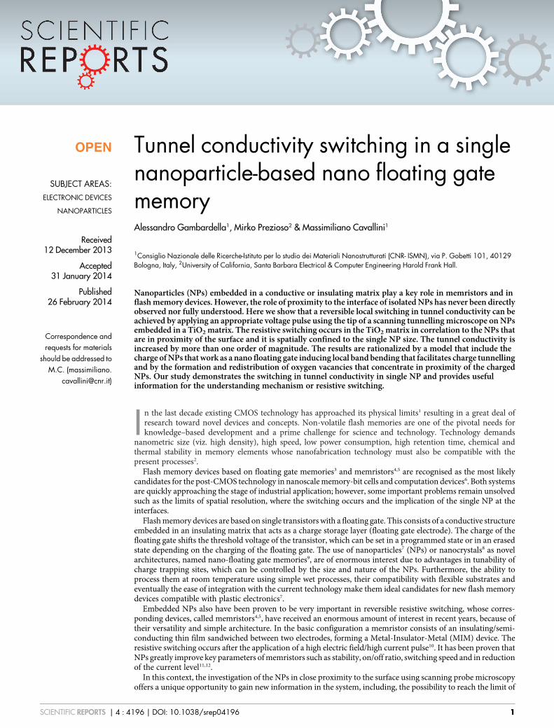
Although, occasionally, some outgrowths exhibit a higher TunnelConductivity (TC) than the matrix, most likely due to the localformation of defects26 or to two-dimensional phases with reducedbandgap27; the CITS map appear generally homogeneous with a TCof about 10 pA/V recorded at 21 V bias (Fig. 2a), which is almostequal to the TC of the blank samples.
The TC can be locally switched in correlation to the particular NPsby applying an appropriate voltage pulse (tip conditioning). When apositive pulse, higher than 15 V and longer than 10 ms, was appliedin correspondence to the NP (Note: these parameters depend on thecurrent of the set-point used before the pulse), we observed a dra-matic change of TC that switches in a conductive state more than oneorder of magnitude higher than the matrix (HCS). The effect is notobserved applying pulses in between the NPs and in blank samples.When applying pulses shorter than 100 ms the morphology remainsunaltered, on the other hand, upon applying a longer and/or higherbias we observed a progressive damaging of the surface associated tothe increase of TC. Figure 2 shows the effect of conditioning onisolated NPs after applying a pulse of 15 V for 50 ms.
It must be noted that while the STM junction occurs in a fewAngstroms (= than 1 pixel in the TC map), the resistive switchinginvolves and is limited to the whole NP region. The change of TC is
Figure 1 | (a) AFM morphology recorded in intermittent contact mode of
cobalt nanoparticles embedded in TiO2 matrix (Z scale 0–15 nm) and (b)
the corresponding scanning kelvin probe microscopy.
Figure 2 | STM and tunnel conductivity map of a Co NP embedded inTiO2 matrix. Topographic images were recorded at 21.5 V and levelled by
2nd order line. (a) Topography before conditioning, the regular
distribution of small spikes is generated by the acquisition of the
corresponding CITS map (Z scale 0–5 nm). (b) Corresponding tunnel
conductivity (TC) map of ‘‘a’’ recorded at 21 V. The spectroscopic points
are recorded with a resolution 5 times less than the topography. Z scale 0–
250 pA/V, Bright zones correspond to lower TC. (c) Topography after
conditioning applying a single pulse of 15 V for 50 ms in the position
indicated by the red cross in ‘‘a’’ (Z scale 0–5 nm). (d) TC map after the
conditioning (switching) recorded at 21 V. While the topography
remains unaltered, the NP at the centre of the image switches from a low
conductive state to a high conductive state; the process is reversible.
www.nature.com/scientificreports
SCIENTIFIC REPORTS | 4 : 4196 | DOI: 10.1038/srep04196 2
reversible upon applying a negative pulse bias. However, whileswitching a NP to HCS can be easily performed by a single pulse,the inverse process is more difficult and several scans or pulses atlarge negative bias are necessary to reset the system which shows aprogressive decreasing of TC instead of a single switching event. Wewere not able to switch the system in high HCS by applying negativebias. Upon increasing the time of conditioning up to 300 ms thesurface of blank TiO2 can also be modified. In this last case bothpositive and negative bias have the same effect producing a moderateincrease of the TC. In this last case the conditioning dramaticallydamages the surface in an area of a few hundred nanometers and it isnot reversible. We propose that in this case the electric field andcurrent density are high enough to cause a thermal recrystallizationforming the so called filaments. This phenomenon is well known andit is believed to be responsible for the so called ‘‘forming’’ step inconventional memristor based on TiO2 in MIM structures5,28.
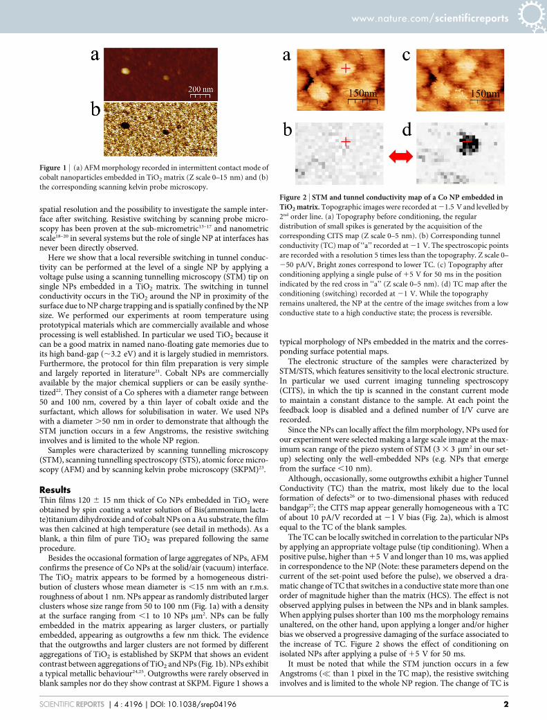
A detailed study of the I-V curves (Fig. 3), helps us to identify thenature the resistive switching on single NP. The I-V curves recordedin a clean sample, before the resistive switching, show the normalbehaviour of freshly prepared TiO2
26,29, both in the matrix and inrelation to the NPs (Blue curve). The typical trend of a n-type semi-conductor with an asymmetric band-gap of ,3.2 eV is expressed bythe zero conductance region around 0 V bias (Curve bleu in fig. 3).This behaviour indicates that a thin layer of TiO2 also covers thepartially embedded NPs. Very rarly, exposed NPs exhibiting metallicbehaviour in I-V curves were observed by STM, we excluded thesezones from our experiments. Figure 3 shows the I-V curves recordedcorresponding to the NP during the application of 15 V pulse biasfor 50 ms and the corresponding dI/dV curve.
Since the pulse bias does not alter the matrix, the I-V curvesobserved before the resistive switching are the typical curves ofTiO2. After resistive switching, the curves recorded in correspond-ence to the NPs narrows the zero conduction region from ,3.2 to,2 eV (Fig. 3b). Noticeably this reduction occurs only in the nega-tive branch of the curve (i.e. when the electrons move from the tip tothe surface) while the positive branch remains almost unaltered. Thisindicates that some empty surface states are formed in the zonecorresponding the NPs, with energy ,1 eV below the conductionband of TiO2. The I-V curve comes back in the original state as thetransition is reset by applying negative pulses.
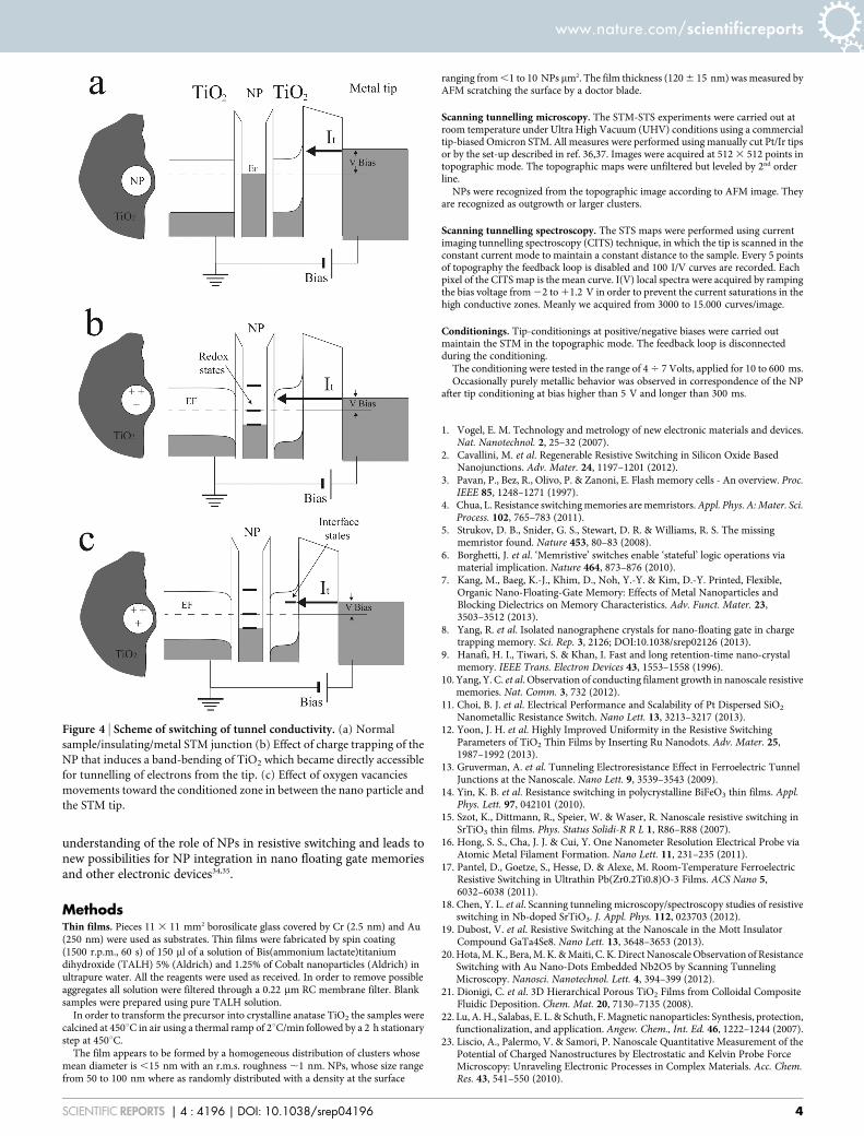
DiscussionAbout the resistive switching that occurs only in correspondence tothe NPs we speculate on the contribution of two effects:
i. The charge injection inside a NP8,30, which occurs at a high biasby direct tunnelling in the NP. This is confirmed by the TCchanges upon conditioning over the entire NP region, not onlyunder the tip during the switching pulse. The switching in TC isnot observed in blank samples, unless the dramatic damage ofthe surface (TiO2 recrystallization).
i. As observed in previous literature31, the positive pulse injectsholes into the NP, which become positively charged. Thecharged NPs in proximity of the surface, work as a floating gate,inducing a band bending towards a lower energy state due to theelectrons in the TiO2 being attracted by the charged NPs. Thesestates are present in the thin layer in between the STM tip and thesurface become accessible as empty states for tunnelling from theSTM tip (Fig. 4b) at energy below the conduction band of TiO2.
i. The injection of electrons in a positively charged NP dischargesthe NP, thereby resetting the system.
ii. A further contribution to resistive switching can be provided bythe formation and redistribution of oxygen vacancies that areintrinsically present TiO2 matrix. By applying pulse bias, theoxygen vacancies form and move toward tip/TiO2/NP interfaceforming undefined TiOx chemical species, which in turn maycreate interface state and/or reduce barrier height. Such areduced barrier effect is well known in Pt/TiO2/Pt memristorsystem32 (Fig. 4c). In addition, NPs may enhance the effect asrecently observed for ruthenium nano-dots embedded in TiO2
12.Figure 4 shows a scheme of the proposed switching mechanismsin TC.
For both models the possible origin of the asymmetry in theswitching behaviour (i.e. the fact that the switching only occurs byinjecting holes but does not work when injecting electrons) can beattributed to the redox states in the NPs related to the oxidation ofsome Co atoms, which form Co ions positively charged, as previouslyobserved in Co NPs deposited on graphite33. The injection of elec-trons should include an improbable chemical reduction of Co atoms.
In summary, we used STM to study the effect of NPs embedded ina TiO2 matrix on the switching of tunnel conductivity. We haveshown how resistive switching occurs in the surface state of the thinlayer of TiO2, in proximity of the NPs and is spatially confined in theregion between the NPs and the surface. The formation of emptysurface states locally enhances the tunnel conductivity reducing theapparent band-gap of the TiO2. Using STM we measured the NPs onthe surface, however we expect that the similar mechanism of TCswitching occurs also inside the matrix, in this case the processinvolve two NPs instead a NPs and the STM tip. Here we proposedtwo possible contributions to TC switching, however we do notexclude that other effects could contribute to the observed switching.In forthcoming work, details of TC switching mechanism will befurther investigated. In addition, the size of NPs can be significantlyreduced to a few nanometres. This ongoing work will lead a better
Figure 3 | Scanning tunnelling spectroscopy. (a) I-V curves extracted
from current imaging tunnelling spectroscopy (CITS) map, before (blue
curve), and after (red curve) the conditioning of the nanoparticle. The
process is reversible. The curve after conditioning was limited in the range
22.5 V–11 V in order to prevent out of range of the STM current.
(b) Corresponding dI/dV curve local density of the surface states.
www.nature.com/scientificreports
SCIENTIFIC REPORTS | 4 : 4196 | DOI: 10.1038/srep04196 3
understanding of the role of NPs in resistive switching and leads tonew possibilities for NP integration in nano floating gate memoriesand other electronic devices34,35.
MethodsThin films. Pieces 11 3 11 mm2 borosilicate glass covered by Cr (2.5 nm) and Au(250 nm) were used as substrates. Thin films were fabricated by spin coating(1500 r.p.m., 60 s) of 150 ml of a solution of Bis(ammonium lactate)titaniumdihydroxide (TALH) 5% (Aldrich) and 1.25% of Cobalt nanoparticles (Aldrich) inultrapure water. All the reagents were used as received. In order to remove possibleaggregates all solution were filtered through a 0.22 mm RC membrane filter. Blanksamples were prepared using pure TALH solution.
In order to transform the precursor into crystalline anatase TiO2 the samples werecalcined at 450uC in air using a thermal ramp of 2uC/min followed by a 2 h stationarystep at 450uC.
The film appears to be formed by a homogeneous distribution of clusters whosemean diameter is ,15 nm with an r.m.s. roughness ,1 nm. NPs, whose size rangefrom 50 to 100 nm where as randomly distributed with a density at the surface
ranging from ,1 to 10 NPs mm2. The film thickness (120 6 15 nm) was measured byAFM scratching the surface by a doctor blade.
Scanning tunnelling microscopy. The STM-STS experiments were carried out atroom temperature under Ultra High Vacuum (UHV) conditions using a commercialtip-biased Omicron STM. All measures were performed using manually cut Pt/Ir tipsor by the set-up described in ref. 36,37. Images were acquired at 512 3 512 points intopographic mode. The topographic maps were unfiltered but leveled by 2nd orderline.
NPs were recognized from the topographic image according to AFM image. Theyare recognized as outgrowth or larger clusters.
Scanning tunnelling spectroscopy. The STS maps were performed using currentimaging tunnelling spectroscopy (CITS) technique, in which the tip is scanned in theconstant current mode to maintain a constant distance to the sample. Every 5 pointsof topography the feedback loop is disabled and 100 I/V curves are recorded. Eachpixel of the CITS map is the mean curve. I(V) local spectra were acquired by rampingthe bias voltage from 22 to 11.2 V in order to prevent the current saturations in thehigh conductive zones. Meanly we acquired from 3000 to 15.000 curves/image.
Conditionings. Tip-conditionings at positive/negative biases were carried outmaintain the STM in the topographic mode. The feedback loop is disconnectedduring the conditioning.
The conditioning were tested in the range of 4 4 7 Volts, applied for 10 to 600 ms.Occasionally purely metallic behavior was observed in correspondence of the NP
after tip conditioning at bias higher than 5 V and longer than 300 ms.
1. Vogel, E. M. Technology and metrology of new electronic materials and devices.Nat. Nanotechnol. 2, 25–32 (2007).
2. Cavallini, M. et al. Regenerable Resistive Switching in Silicon Oxide BasedNanojunctions. Adv. Mater. 24, 1197–1201 (2012).
3. Pavan, P., Bez, R., Olivo, P. & Zanoni, E. Flash memory cells - An overview. Proc.IEEE 85, 1248–1271 (1997).
4. Chua, L. Resistance switching memories are memristors. Appl. Phys. A: Mater. Sci.Process. 102, 765–783 (2011).
5. Strukov, D. B., Snider, G. S., Stewart, D. R. & Williams, R. S. The missingmemristor found. Nature 453, 80–83 (2008).
6. Borghetti, J. et al. ‘Memristive’ switches enable ‘stateful’ logic operations viamaterial implication. Nature 464, 873–876 (2010).
7. Kang, M., Baeg, K.-J., Khim, D., Noh, Y.-Y. & Kim, D.-Y. Printed, Flexible,Organic Nano-Floating-Gate Memory: Effects of Metal Nanoparticles andBlocking Dielectrics on Memory Characteristics. Adv. Funct. Mater. 23,3503–3512 (2013).
8. Yang, R. et al. Isolated nanographene crystals for nano-floating gate in chargetrapping memory. Sci. Rep. 3, 2126; DOI:10.1038/srep02126 (2013).
9. Hanafi, H. I., Tiwari, S. & Khan, I. Fast and long retention-time nano-crystalmemory. IEEE Trans. Electron Devices 43, 1553–1558 (1996).
10. Yang, Y. C. et al. Observation of conducting filament growth in nanoscale resistivememories. Nat. Comm. 3, 732 (2012).
11. Choi, B. J. et al. Electrical Performance and Scalability of Pt Dispersed SiO2
Nanometallic Resistance Switch. Nano Lett. 13, 3213–3217 (2013).12. Yoon, J. H. et al. Highly Improved Uniformity in the Resistive Switching
Parameters of TiO2 Thin Films by Inserting Ru Nanodots. Adv. Mater. 25,1987–1992 (2013).
13. Gruverman, A. et al. Tunneling Electroresistance Effect in Ferroelectric TunnelJunctions at the Nanoscale. Nano Lett. 9, 3539–3543 (2009).
14. Yin, K. B. et al. Resistance switching in polycrystalline BiFeO3 thin films. Appl.Phys. Lett. 97, 042101 (2010).
15. Szot, K., Dittmann, R., Speier, W. & Waser, R. Nanoscale resistive switching inSrTiO3 thin films. Phys. Status Solidi-R R L 1, R86–R88 (2007).
16. Hong, S. S., Cha, J. J. & Cui, Y. One Nanometer Resolution Electrical Probe viaAtomic Metal Filament Formation. Nano Lett. 11, 231–235 (2011).
17. Pantel, D., Goetze, S., Hesse, D. & Alexe, M. Room-Temperature FerroelectricResistive Switching in Ultrathin Pb(Zr0.2Ti0.8)O-3 Films. ACS Nano 5,6032–6038 (2011).
18. Chen, Y. L. et al. Scanning tunneling microscopy/spectroscopy studies of resistiveswitching in Nb-doped SrTiO3. J. Appl. Phys. 112, 023703 (2012).
19. Dubost, V. et al. Resistive Switching at the Nanoscale in the Mott InsulatorCompound GaTa4Se8. Nano Lett. 13, 3648–3653 (2013).
20. Hota, M. K., Bera, M. K. & Maiti, C. K. Direct Nanoscale Observation of ResistanceSwitching with Au Nano-Dots Embedded Nb2O5 by Scanning TunnelingMicroscopy. Nanosci. Nanotechnol. Lett. 4, 394–399 (2012).
21. Dionigi, C. et al. 3D Hierarchical Porous TiO2 Films from Colloidal CompositeFluidic Deposition. Chem. Mat. 20, 7130–7135 (2008).
22. Lu, A. H., Salabas, E. L. & Schuth, F. Magnetic nanoparticles: Synthesis, protection,functionalization, and application. Angew. Chem., Int. Ed. 46, 1222–1244 (2007).
23. Liscio, A., Palermo, V. & Samori, P. Nanoscale Quantitative Measurement of thePotential of Charged Nanostructures by Electrostatic and Kelvin Probe ForceMicroscopy: Unraveling Electronic Processes in Complex Materials. Acc. Chem.Res. 43, 541–550 (2010).
Figure 4 | Scheme of switching of tunnel conductivity. (a) Normal
sample/insulating/metal STM junction (b) Effect of charge trapping of the
NP that induces a band-bending of TiO2 which became directly accessible
for tunnelling of electrons from the tip. (c) Effect of oxygen vacancies
movements toward the conditioned zone in between the nano particle and
the STM tip.
www.nature.com/scientificreports
SCIENTIFIC REPORTS | 4 : 4196 | DOI: 10.1038/srep04196 4

24. Nonnenmacher, M., O’Boyle, M. P. & Wickramasinghe, H. K. Kelvin probe forcemicroscopy. Appl. Phys. Lett. 58, 2921–2923 (1991).
25. Liscio, A., Palermo, V., Mullen, K. & Samori, P. Tip-Sample Interactions in KelvinProbe Force Microscopy: Quantitative Measurement of the Local SurfacePotential. J. Phys. Chem. C 112, 17368–17377 (2008).
26. Lin, Y., Lin, R., Wang, W. & Xiao, X. Characterization of TiO2 nanocrystallinethin film by scanning tunneling microscopy and scanning tunnelingspectroscopy. Appl. Surf. Sci. 143, 169–173 (1999).
27. Tao, J. G., Luttrell, T. & Batzill, M. A two-dimensional phase of TiO2 with areduced bandgap. Nature Chem. 3, 296–300 (2011).
28. Kwon, D. H. et al. Atomic structure of conducting nanofilaments in TiO2 resistiveswitching memory. Nat. Nanotechnol. 5, 148–153 (2010).
29. Berko, A. & Solymosi, F. Study of Clean TiO2(110) Surface by Scanning TunnelingMicroscopy and Spectroscopy. Langmuir 12, 1257–1261 (1996).
30. Lee, C., Kim, I., Shin, H., Kim, S. & Cho, J. Nonvolatile memory properties of Ptnanoparticle-embedded TiO2 nanocomposite multilayers via electrostatic layer-by-layer assembly. Nanotechnology 21, 185704 (2010).
31. Yang, J. et al. Electrostatic force microscopy measurements of charge trappingbehavior of Au nanoparticles embedded in metal-insulator-semiconductorstructure. Ultramicroscopy 108, 1215–1219 (2008).
32. Yang, J. J. et al. Memristive switching mechanism for metal/oxide/metalnanodevices. Nat. Nanotechnol. 3, 429–433 (2008).
33. Fetting, J. et al. I-V characteristics of single and clustered ligand stabilized cobaltnanoparticles on highly oriented pyrolytic graphite obtained with conductingatomic force microscopy under ambient conditions. J. Appl. Phys. 112, 104327(2012).
34. Cavallini, M. et al. Additive nanoscale embedding of functional nanoparticles onsilicon surface. Nanoscale 2, 2069–2072 (2010).
35. Simeone, F. C., Albonetti, C. & Cavallini, M. Progress in Micro- andNanopatterning via Electrochemical Lithography. J. Phys. Chem. C 113,18987–18994 (2009).
36. Cavallini, M. & Biscarini, F. Electrochemically etched nickel tips for spin polarizedscanning tunneling microscopy. Rev. Sci. Instrum. 71, 4457–4460 (2000).
37. Cavallini, M., Aloisi, G., Bracali, M. & Guidelli, R. An in situ STM investigation ofuracil on Ag(111). J. Electroanal. Chem. 444, 75–81 (1998).
AcknowledgmentsWe thank Zhara Hemmatian Denis Gentili and Vittorio Morandi for sample preparationand SEM measurements and Tobias Cramer for the useful discussion and the help to modelthe process and Laurel L. McClure for editing the manuscript. A.G. was supported byEU-FP7 project NMP3-LA-2010-246102 (IFOX), the work was partially supported by‘‘Progetto bandiera NANOMAX-N-CHEM’’.
Author contributionsA.G. was responsible for all the experiments described in this article; M.P. was partiallyresponsible for preparation of the paper and modeling; M.C. was responsible for designingand providing guidance for the experiments and for editing and proofreading the paper. Allthe authors contributed to write the manuscript.
Additional informationCompeting financial interests: The authors declare no competing financial interests.
How to cite this article: Gambardella, A., Prezioso, M. & Cavallini, M. Tunnel conductivityswitching in a single nanoparticle-based nano floating gate memory. Sci. Rep. 4, 4196;DOI:10.1038/srep04196 (2014).
This work is licensed under a Creative Commons Attribution-NonCommercial-NoDerivs 3.0 Unported license. To view a copy of this license,
visit http://creativecommons.org/licenses/by-nc-nd/3.0
www.nature.com/scientificreports
SCIENTIFIC REPORTS | 4 : 4196 | DOI: 10.1038/srep04196 5