Embed Size (px)
Citation preview
Unites" a r 1. States tent 1191 Wakamatsu et a1.
1541
1751
1731
122] [21]
130]
1521 1511 [531
1561
3,564,280 3,634.826
TIME MULTIPLEXED ELECTRIC WIRING SYSTEM FOR CONTROL AND MONITORING OF FIELD POINTS
Inventors: Hisato Wakamatsu; Hiroshi Arai, both of Toyota; Akira Kuno, Nagoya; Shigeyuki Akita, Okazaki, all of Japan
Assignees: Nippon Soken, Inc., Nishio; Toyota Jidosha Kogyo Kabushiki Kaisha, Toyota, both of Japan
Filed: July 26, 1974
Appl. No.: 492,204
Foreign Application Priority Data July 28, 1973 Japan .............................. .. 48-85130
US. Cl. .............................................. .. 340/163
Int. Cl.2 ......................................... .. H04Q 9/00
Field of Search ......... .. 340/147 LP, 163, 167 R
References Cited UNITED STATES PATENTS
2/1971 Sognefest ...................... .. 340/163 X
l/l972 Biederman ................... .. 340/167 R
B‘! _L_____
B2 , DETECTING I SECTION
ACTUATING SECTION
1g.
[11] 3,952,26 145] Apr. 20, 1976
3,701,101 10/1972 Hei7. . . . . . . . . . . t . . . t . . . . . . . . .. 340/163
3,818,447 6/1974 ' Craft ....................... .. 340/147 LP
3,821,706 6/1974 Bennett et a1. . . . . . . . . t . . . . I . . .. 340/163
3,828,313 8/1974 Schull et all ................... .. 340/163
3,854,122 12/1974 Cross ............................ .. 340/163 X
vPrimary Examiner—Donald J. Yusko Attorney, Agent, or Firm—Cushman, Darby & Cushman
[57] ABSTRACT There is provided an electric wiring system in which a plurality of'electric components, a plurality of com mand switches for actuating the electric components and a plurality of sensors, etc., are provided at various points of an automotive vehicle, transmitting and re ceiving units of time-shared pulse transmission type which are arranged at the various points of the vehicle are interconnected through a plurality of electric wires or lines, the electric components or loads are divided into a plurality of locals each thereof including a group of the loads, and the transmission and reception of information between the respective locals and a command section is effected by a time-shared pulse transmission method, whereby reducing the hazard of short‘circuit fault.
9 Claims, 7 Drawing Figures
US. Patent April 20, 1976 ‘ Sheet 1 Of6 3,952,286
51 F l G . I _ I _
~82 DETECTING > Ax. SECTION v.
Bl __ __ I
B4 g ' l A‘) A2 I I j I
RECEWER RECEIVER ACTUATING SECTION “'SECT ION SECTION
I_—"'_ ML‘ : LOADSECTION I 'ggérfl’oN I NI-Z ACTuATTNC j
+0 WJLB SECTION I —§___ __ \‘A4 _ A3
. -C _\ x
83 H/ L5, 6 _ D , L r]
__ ET] __ 4 Y ‘ 9| I
IE2 El? I T ' I = ' = "'S ' DETECTING
TRANSMI'ITER SECTION - SECTION
A : : I C4~ SECCTHO‘NWG TING ACTUATING . v SECTION SECTION N ' :
E4 C3~LOAO SECTION __ L92
LOAD XE -— F 3 SECTION 3 __ . __
r F' ~l-F6 OSCILLATOR I
- - I TRANSNIIIIER " RECEIVER SECT'ON SECTION
I
, DETECTING 2 ' LOGICAL SECTION I
PROCESSING SECTION
64) |——j TRANSMITTER , RECEIVER
I ACTUATING SECmN ""6 SECTION —] LGI
_~_'§ " L_‘— DETECTING :
62 N SECTION
Sheet 2 of 6 3,952,286 US. Patent April 20, 1976
N
V6016 QZFZDOO
U.S. Patent April 20, 1976 Sheet 3 of6 3,952,286
ICEMHEEREEEEEEQJLEEhVEEEEE? q a = c a a d
o mmwi--- m: i--- N _ 0 8m vmw lllll I m: lllll i m N _ 0 8y
: I = z I = I
NNVF: wmvsv mwv AZ“ vmv. =>: MN? “I: WNW 3: 5v 2; En *3 m5 2.: m5 28 EM T: Em m: R: m5 8“ In “my 0513
US. Patent April 20, 1976 Sheet 5 of6 3,952,286
?gbgbé Fmmkmp H
\INE. @NE. mNEr VNE. MNE. NNE. _ MEI
US. Patent April 20, 1976 Sheet 6 of6 3,952,286
ETRZ
3,952,286 1
TIME MULTIPLEXED ELECTRIC WIRING SYSTEM FOR CONTROL AND MONITORING OF
FIELD POINTS
BACKGROUND OF THE INVENTION
1. Field of the Invention The present invention relates to an electric wiring
system in which a plurality of electric components 10 (such as head lamps), a plurality of command switches for actuating the electric components and a plurality of sensors are arranged at various points of a vehicle, particularly an automotive vehicle, and the actuation of the electric components is effected by means of a plu rality of time-shared pulse transmission type transmit ting and receiving units which are suitably arranged at various points of the vehicle and which are intercon< nected by means of a plurality of lines.
2. Description of the Prior Art In known electric wiring systems, it has been custom
ary to use as many electric wires or cables as there are independent electric components to carry electricity between a group of such electric components and a group of command switches. Consequently, this con ventional electric wiring system requires a large num ber of heavy wires for carrying electricity, thus not only increasing the costs required for the electric wiring of the vehicle, but also increasing the volume and weight of the wires with resultant wiring difficulties. In addi tion, the probability of occurrence of a short~circuit between the vehicle body and the individual electric components is correspondingly high.
SUMMARY OF THE INVENTION
It is an object of the present invention to provide an electric wiring system in which groups of electric com ponents or loads are divided into separate locals, and the transmission and reception of information between the individual locals and a command section is accom plished by a time-sharing pulse method, whereby re ducing the cost, volume and weight of the wires used and decreasing the probability of occurrence of short circuit fault.
It is another object of the present invention to pro vide such electric wiring system which can be satisfac— torily handled by those mechanics who engage in ordi nary servicing of automobiles and who do not possess any specialized knowledge required for handling the conventional time-sharing pulse systems. The principle of the invention, together with addi
tional objects and advantages thereof will be best un derstood from the following detailed description of a speci?c embodiment taken in conjunction with the accompanying drawing.
BRIEF DESCRIPTION OF THE DRAWING
FIG. 1 is a block diagram showing the general con struction of an electric wiring system according to the present invention. FIG. 2 is a block diagram showing the internal con
struction of a transmitter and receiver unit used in the system of this invention. FIG. 3 is a diagram showing the waveforms generated
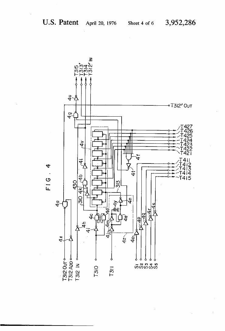
at various points in the system of the invention. FIG. 4 is a wiring diagram showing the detailed cir
cuit construction of the counting block used in the transmitting and receiving unit shown in FIG. 2.
15
25
35
45
50
55
60
65
2 FIG. 5 is a wiring diagram showing the detailed cir
cuit construction of a transmitting and receiving block forming part of the transmitter and receiver unit shown in FIG. 2. FIGS. 6a and 6b are block diagrams showing the
interconnections of the transmitter and receiver units of the form shown in FIG. 2.
DESCRIPTION OF THE PREFERRED EMBODIMENT
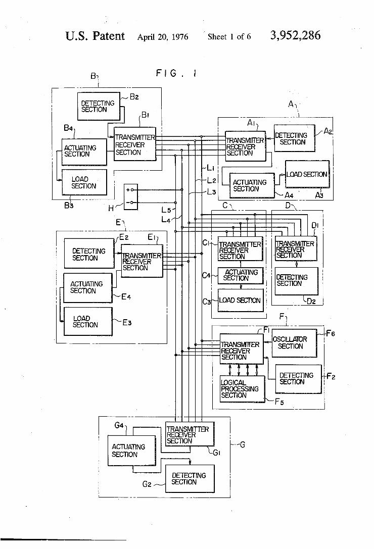
Referring ?rst to the block diagram of FIG. 1 show ing the general construction of the entire automobile electric wiring system of the invention, a total of 7 blocks are provided, i.e., blocks A and B (hereinafter referred to as locals A and B) which respectively detect and control the condition and operation of left and right groups of devices installed in the engine room, a block C (hereinafter referred to as a local C) for con trolling a group of instruments mounted on an instru ment panel, a block D (hereinafter referred to as a local D) for detecting the condition of a group of de vices mounted on a steering wheel column, a block E (hereinafter referred to as a local E) for detecting and controlling the condition and operation of a group of devices installed in a console box assembly, a block G (hereinafter referred to as a local G) for controlling a rear combination lamp, and a block F (hereinafter referredto as a local F) which serves as a logical pro cessing section for the whole automobile. The respec tive locals A, B, C, D, E, F and G are interconnected only with three signal lines L, , L2 and L3 and two sup ply lines L4 and L5 (positive and negative lines) con nected to a battery H.
In the local A, symbol A, designates a transmitter and receiver section, A2 a detecting section comprising a plurality of detecting means composed of switches and sensors for detecting the condition of a group of de vices, A3 a group of devices such as lamps and motors (hereinafter referred to as a load section), A,4 an actu ating section for actuating the loads in the load section in response to the output of the transmitter and re ceiver section A,. Similarly, in the local B, symbol B, designates a transmitter and receiver section, B, a de tecting section, B3 a load section, B4 an actuating sec tion. In the local C, symbol C, designates a transmitter and receiver section, C3 is a load section, C,, an actuat ing section; in the local D, D, a transmitter and receiver section, D2 a detecting section; in the local E, E, a transmitter and receiver section, E2 a detecting section, B, a load section, B,, an actuating section; in the local G, G, a transmitter and receiver section, G2 a load section, G4 an actuating section; in the local F, F, a transmitter and receiver section, F2 a detecting section, F5 a logical processing section, F6 an oscillator section for generating reference and synchronizing signals.
In FIG. 1, detecting sections A,, B2, D2, E2 and F2, and load sections A,,, B3, C3 and E3, form terminating means.
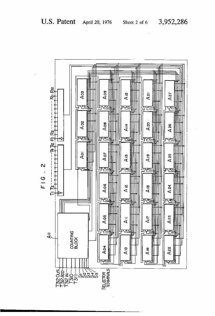
FIG. 2 is a block diagram showing one form of the transmitter and receiver units used in the respective local blocks. In FIG. 2, symbol A,, designates a count ing block, A0,, A02, . . . , A27 transmitting and receiving blocks which serve the double function of transmitting and receiving signals, i.e., the transmitting and receiv ing blocks of the same type each thereof having both a transmitting circuit and a receiving circuit. Each of the transmitter and receiver sections A,, B,, C,, D,, E,, G, and F, of the locals A, B, C, D, E, G and F includes a
3,952,286 3
plurality of the transmitter and receiver units shown in FIG. 2. This transmitter and receiver unit is usually. fabri
cated in the form of a large scale integration (LSI) device, and the single counting block A“ is selectively connected to the plurality of transmitting and receiving blocks A0,, A02, . . . , A27 in accordance with the combi
nation of signals applied to selector terminals 8,, S2, S3, S4 and S5 which may be either 0 or 1. Consequently, if the number of the selector terminals used is ?ve, the number of the transmitting and receiving blocks is not limited to 27 as in the case of FIG. 2, but it may be increased to the maximum number of 32. In case the number of the selector terminals used is 6, then as many as 64 transmitting and receiving blocks may be used. Terminals T1, T2, . . . , T12 are connected to sen
sors which detect the condition of the respective elec tric devices assigned to the same local block, while terminals R1, R2, . . . , R2 are connected to actuating means which control the operation of the respective electric devices assigned to the same local block. A plurality of signal lines each respectively connected from each of said terminals T1, T2, . . . T12 and R1, R2 . . . R12 to each of said receiving blocks A01, A02 . . . A27, are indicated, for convenience of illustration, by one line in FIG. 2. Designated T3120“, and T312add are connecting terminals to other transmitter and receiver units in the same block, and T312,,,, T310 and T311 designate connecting terminals to other local blocks. The selection of the transmitting and receiving blocks is accomplished in the following manner. When it is desired to bring the transmitting and receiving blocks A04 and A05 into operation so that the signals from the switches or sensors in the same local are transmitted to
the locals and signals are received from the other local to drive the loads such as the lamps or motors in the same local, the selector terminals S1‘, S2, S3, S, and S5 in one transmitter and receiver unit of the type shown in FIG. 2 are respectively set to 0, 0, 1, O and 0 signals to select and allow only the transmitting and receiving block A0,, to perform the transmitting and receiving functions, while the selector terminals 8,, S2, S3, S4 and S5 in another transmitter and receiver unit are respec tively set to 1, 0, l, 0 and 0 signals to select and allow only the transmitting and receiving block A05 to per form the transmitting ‘and receiving functions. In this way, the local A of FIG. 1 can serve the function of transmitting and receiving the necessary signals. On the other hand, if it is desired to bring, in the local B, the transmitting and receiving blocks A01, A02 and A03 into operation to send the signals from the switches or sen sors in the local B to the other locals and receive signals therefrom to actuate the loads such as the lamps or motors in the local B, the local B of FIG. 1 can serve all the necessary functions of transmitting and receiving the necessary signals by means of a total of three trans mitter and receiver units, i.e., the ?rst transmitter and receiver unit in which the selector terminals 8,, S2, S3, S4 and S5 (FIG. 2) are set to l, O, 0, 0 and 0 to select and allow only the transmitting and receiving block A01 to perform its transmitting and receiving functions, the second transmitter and receiver unit in which the selec tor terminals 8,, S2, S3, S4 and 8,, are set to 0, 1, O, O and 0 to select and allow only the transmitting and receiv— ing block A02 to perform its transmitting and receiving functions and the third transmitter and receiver unit in which the selector terminals 5,, S2, S3, S, and S5 are set to l, 1, 0, 0 and O to select and allow only the transmit
25
45
55
60
65
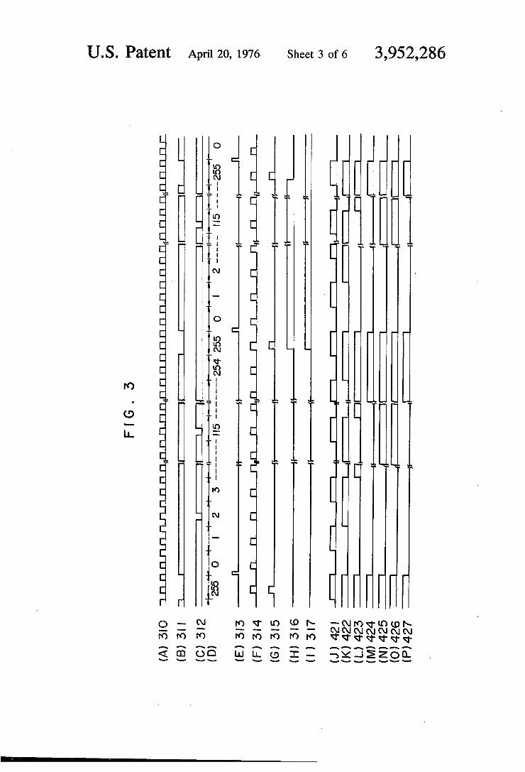
4 ting and receiving block A03 to perform its transmitting and receiving functions. This applies equally to other locals C, D, E, F and G, and the transmitter and re ceiver section of each local performs its desired func tions by setting the selector terminals 8, to S5 of the necessary transmitter and receiver units of the same construction as shown in FIG. 2 to either 1 or O in the above-described manner. Referring now to the signal waveforms of FIG. 3
which are generated at various points of the circuitry, the principle of the time-sharing pulse transmission method used with the embodiment shown in FIG. 1 will be outlined. Here, the time-sharing means a process in which the time base is divided as shown in FIG. 3(D) into equal periods, that is, smaller intervals 000, O01, O02, . . . , 255 (hereinafter referred to as addresses),
and the transmission and reception of signals among the transmitter and receiver sections of the respective locals are effected during the corresponding addresses. The above-described time-shared addresses are pro~
vided by the counting blocks in the transmitter and receiver units of the respective locals on the basis of the synchronous signal 311 shown in FIG. 3(B) and the timing signal 310 shown in FIG. 3(A) which are deliv ered from the local F of FIG. 1, and these counting blocks generate address signals corresponding to these time-shared intervals. The signals to be transmitted from the transmitting side of the transmitter and re ceiver section in each local are combined and transmit ted in the form of the level signal 312 shown in FIG. 3(C). Therefore, the transmission of signals among the respective locals are effected through three lines, i.e., lines L1, L2 and L3 which respectively deliver the syn chronous signal 311, the timing signal 310 and the level
,signal 312, while two additional lines L4 and L5 are provided for the purpose of power feeding. The syn chronous signal 311 in which the address 255 of the time-shared addresses 000, 001, 002, . . . , 255 has a low level is distributed to the counting block in each transmitter and receiver unit to produce from this sig nal 311 the reset signal 313 shown in FIG. 3(E) and this reset signal 313 is used to reset the frequency dividing circuit in the counting block. Each time-shared interval is superseded by the succeeding one every second pe riod of the timing signal 310. Thus, the frequency divid ing circuits provided in the transmitter and receiver units in the transmitter and receiver sections of the respective locals operate all in synchronism. The trans mission of signals from the local A to any other local on the level signal 312 is effected as follows. One of the transmitting and receiving blocks Am through A27 is preliminarily selected through the selector terminals 8,, S2, S3, S4 and S5 in each of the plurality of the transmit ter and receiver units of FIG. 2, and then three input signals, i.e., a predetermined input signal to be trans mitted, an address signal from the frequency dividing circuit corresponding to the time-shared address (such as the address 002 or 1 15) to which the input signal is allotted, and the strobe signal 314 shown in FIG. 4(F) are applied to an AND gate and the resultant level signal 312 is transmitted to any of other locals B, C, D, E, G and F. Similarly, the transmission of signals from each of the locals B, C, D, E, G and F to any other local is accomplished by means of the level signal 312 pro duced through the same process of operation just de~ scribed. For example, the level signal 312 shown in FIG. -3(C) shows the case in which the signals to be transmitted ‘are superposed respectively on the time
3,952,286 5
shared addresses-002 and 115. In accordance with ‘the thus transmitted level signal 312 having ‘the signal su~ perposed on the address 002 or 115, only the speci?ed transmitting and receiving block (e-.g.-,the'block'Amor A02) in the transmitter and receiver unit (FIG..2) of the particular local of the locals A,.B, C‘, D, E, FKandG ,of FIG. 1 is brought 'into- operation through the prese lected selector terminals S1,. S2, S3, S4 and S510 actuate the load in that particular local. In other words,~~.the initial stateis established by applying to the reset input of a ?rst memory circuit the .reset signalr3l3 shown in FIG. 3(E) and producedbythe low level time-shared address 255.. Then, the outputrsignal of an AND gate which performs the ANDop'eration on the address signal appearing in the predetermined time-shared ad dress and the level signal 312 is applied to the setinput of the ?rst memory circuit.- Consequently, the applica tion of this AND-signal clears the previously- estab lished initial state; while. the initial state=is=maintained when no signal is'applied to .the set input. Namely,‘ the state of the‘?rstmemory circuit is determined. depend ing upon whetherthere'is a- level signal in the respective time-shared intervals. This state'isagain cleared by the following reset signal 313 and; the. initial stateis-re stored. To transfer. thecontent of the ?rst memory circuit to a second memory circuit before the former is cleared, a gateis provided between the ?rst and‘seco'nd memory circuits to control the transmission of signals thereb'etwe'en, and the transfer .:'signal .315 {which is shown in FIG.I3(-G)Yan‘d which is the logical-product of the address 255.and the :strobe signal 314~shown in FIG. 3(F) is applied to-this gate; For instance, if the level signal312 of FIG~.:3(C) has the .transmittingvsignal on the address 022 (or it has a low-level;therein)=, the content of the'r?rst-memoryrcircuit’ is continuouslyfed to and stored in the secondrmemory circuit during‘ the duration of thesignal 316 shown in FIG.» 3(1I-I) from the transfer signal 315 of FIG, 3(G) in the period to the transfer signal 315 in the next period, whereas when the transmitting signal is on the address 115, the con tent of the ?rst memory circuit is continuously stored in the second memory circuit in the similar manner, but during the duration of the signal 317 shown in FIG. 3(I). Therefore, if vthe signal remains on the'address 115 of the level signal 312, the signal 317 also remains
we 5
20
25
40
v6 ‘the frequency dividing circuit 4viin the initial state. The timing signal 310 shown in FIG. 3(A) is applied to the terminal T 310. of FIG. 4 and it is then applied to the inputo? the frequency dividing circuit 4v by way of the .reshaping- circuit constituted ,. by. the NAND gates 40 and 4d and theinverter .gate4i. The NAND gate 412 performsthe logical operation on the timing signal 310 from; the reshaping .circuit and the inverted output signaliof the ?rst :istate ?ip-flop in thefrequency divid ingcircuit 4v, and its output signalis then inverted to . generate thestrobe signal 314 shown in FIG.>3(F). The Eztiming signalq310 is successively frequency divided by -the frequency dividing circuit 4v so that the output signals 421, 422, 423, 424, 425,426‘and 427.respec tively shown.in,FIGS. 3(J),,3(K)', 3(L), 3(M),,3(N), 3(0) and 3(P) are generated from the respective ?ip ?ops. A plurality of signal lines for carrying these out put signals are indicated, for convenience of illustra tion, by one line in the .block diagram of FIG; 2. When ,all of the outputsiof. the frequency, dividing circuit 4v have-a 1 signaLithat is, when the time-‘shared, address 3255 has been“ reached, .the output signal of the NAND gate ‘4f goesvto O. This .Osignal is inverted by the in verter gate 4t and it is then applied to the NAND gate 4g which in turn performs'the logical operation on this invertedsignal and the strobe signal 314 to produce the transfer signal 315 shownin FIG. 3(G.). The ?ve termi nals 8,, 82,83, 8., and S5,,are terminals for selectively operating the transmitting and receivingblocks in the transmitter and receiverjunit. Thus, by settingeach of ,these terminals to either a l or 0 signal, it is possible .to makel5 kinds or 32-kinds of selection.-These signals whichv are eachr-setto either l‘or O. are respectively
‘ inverted by the] inverter gates 40, 4p, 4q, 4r and 4s to produce signals 411, 412,413, 414 and 415. A plurality of signal lines for carrying these output signals are indicated ,' for convenience of illustration, by» one line in ithe block diagram of FIG.~2.=The vsignals described so ‘far are applied to, the respectiveelements of the trans mitting and receivingblocks,Am,.A02,~. A2, in ,the transmitter and receiver unit shown in FIG. 2.
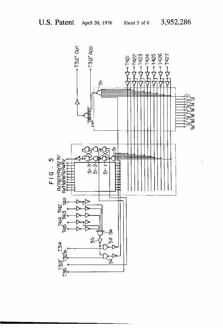
. FIG. 5 illustrates the internal circuit construction of the transmitting and receiving block. The transmitting
' and receiving block of FIG. 5 is composed of NAND
on even after vthe‘transf'er signal 315 in the second _ period. In response to this signal 316 or 3 17, the actuat~ ing means in the actuating section (FIG. 1) which cor responds to the speci?ed address actuates the asso ciated load. ' ‘
The signal transmission according to the above described time-sharing system will now be described with reference to the detailed circuit construction of the component elements in each local. Referring to FIG. 4 illustrating the internal wiring diagram of a counting block, A, in the transmitter and receiver unit shown in FIG. 2, numerals 4a, 4b, 4c, 4d, 4e, 4f and 4g designate NAND gates, 4h, 4i, 4]’, 4k, 4], 4m, 4n, 40, 4p, 4q, 4r, 4s, 413, 4a and 4x inverter gates, 4v a frequency dividing circuit, 4y a capacitor. The inverter gates 4i, 4m and 4n and the NAND gate 4e and the capacitor 4y constitute a reset circuit 4z for the frequency dividing
50
60
circuit 4v. In operation, when the synchronous signal 311 shown inFIG. 3(8) is applied to the terminals T311 in FIG. .4, the NAND gate 4e performs the logical operation on'this signal and the one delayed by the capacitor 4y, and‘ the inverter gate 4n generates at its output the reset signal 313 shown in FIG. 3(E) to place
65
gates and inverter gates, and it is assumed that this block comes into operation only when there are a 1 signal at the terminal 8,, a 0 signal at S2, a 0 signal at S3, a 1 signal at S4 ‘and a 0 signal at S5. In this case, by setting the inputs to the terminals 8,, S2, S3, S4 and S5 shown in FIG. 4 in the manner described above, the output of a NAND gate 5a has a 0 signal and this signal is inverted by an inverter gate 5b. Consequently, the inverted 1 signal opens NAND gates 5c and 5d, and the transmitting and receiving circuits shown in FIG. 5 come into operation. For example, if it is assumed that of the terminals T1, T2, . . . , T12 which are connected to
switches, sensors, etc., the switch terminal T1 corre sponds to the time-shared address 002, the signal 422 of FIG. 3(K), the inverted signals of the signals 421, 423, 424, 425, 426 and 427 respectively shown in FIGS. 3(J), 3(L), 3(M), 3(N), 3(0) and 3(P) and the strobe signal 314 are applied to a NAND gate 5t,. When the switch terminal T, has a 0 signal, it is in verted by an inverter gate and applied to a terminal T,’ so ‘that a terminal T3l2',,,,, in FIG. 5 receives the level
~ signal 312 shown in FIG. 3(C) in which the time-shared ‘ address 002 has a 0 level. This applied equally to other terminals T2, T3, . . . , T2, for the switches, etc., and the
3,952,286 7
address signals 421, 422, 423, 424, 425, 426 and 427 are connected so that the address corresponding to the respective switches and so on can be obtained. On the other hand, assume that of the terminals R1,
R2, . . . , Rm connected to the actuating section for actuating the loads such as wipers and head lamps, the load terminal Rl corresponds to the time-shared ad dress 115. In this case, in the similar manner as de scribed above, the address signals 421, 422, 425 and 426 and the inverted signals of the address signals 423, 424 and 427 are applied to the inputs of a NAND gate Sr, and the level signal 312 shown in FIG. 3(C) and inverted by the inverter gate 4h of FIG. 4 is applied to a terminal T312',-,,. Consequently, the NAND gate 5r produces a 0 output signal only when the time-shared address 115 is reached, and this changes the output of the ?rst memory circuit which has previously been placed in the initial state by the reset signal 313' of FIG. 4 which was applied to a terminal T313’ of FIG. 5. In other words, the output of a NAND gate 5r-l has a 1 signal. The transfer signal 315 of FIG. 4 is applied to the terminal T315 of FIG. 5 so that a NAND gate 5r-2 opens and the content of the ?rst memory circuit is transferred to the second memory circuit. This transfer signal causes a NAND gate 5r-3 to produce a 1 signal at its output and a 0 signal appears at a terminal R1’. Consequently, the 1 signal which was inverted by an inverter gate is applied to the load terminal R, of FIG. 2 and the actuating section is controlled to actuate the corresponding load. To simplify the illustration, cir cuitry, corresponding to that just described, by which signals may be produced at terminals R2’ — R12’, has been replaced by the solid line block in FIG. 5. Further, by connecting a terminal T3l2'add of FIG. 5 to the terminal T312’ou, of other transmitting and receiving blocks, the signals transmitted from the plurality of the transmitting and receiving blocks in the transmitter and receiver unit of FIG. 2 are combined at a terminal T3l2’ou, of the transmitting and receiving block A0, of FIG. 2, and it appears at the terminal T3l2’ou, shown in
20
25
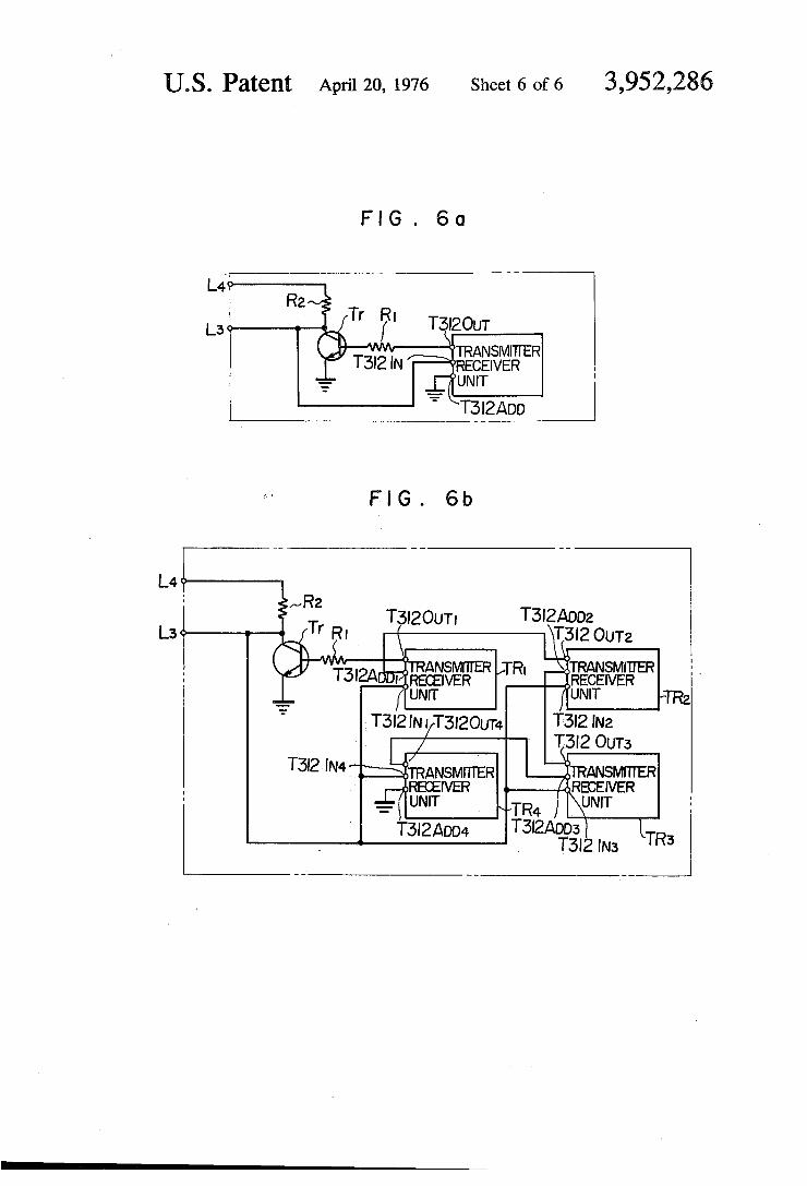
30
FIG. 4 from which it is applied to the NAND gate 4a and this combined signal appears at the output terminal T312,” As shown in FIG. 6a, the signal appeared at the output terminal T3120“, is applied through a resis tor R, to the base of a transistor Tr and its inverted signal appears at the collector thereof. The collector of the transistor Tr is connected to the terminal T312," and it is also connected to the level signal line L3 to transmit and receive signals from any other locals. In the case that a plurality of the transmitter and receiver units are employed to effect the transmission and re ception of signals, as shown in FIG. 6b, a terminal T3120,“ of a ?rst transmitter and receiver and receiver unit TR, is connected to a terminal T312001,” of a sec— ond transmitter and receiver unit TR3 whose terminal T3l2mm, is in turn connected to a terminal T312add2 of a third transmitter and receiver unit TRZ, and a termi nal T312m2 of the transmitter and receiver unit TR2 is in turn connected to a terminal T312add, of a fourth transmitter unit TRl. In this way, the signals to be trans mitted are combined at the terminal T3120," of the transmitting and receiving unit TRl and it is delivered as the level signal 312 to the level signal line L3 through the transistor Tr. In this case, the input signals from the level signal line L3 are applied to the respective termi nals T312,“ of the transmitter and receiver units TR” TR2, TR3 and TR4, thus permitting the transmission and reception of signals with other locals. The method of selecting the desired transmitter and
receiver units will be described more speci?cally with reference to the illustrated embodiment. The following Table l is a list of the addresses assigned to the actuat ing means such as switches, sensors, etc., and the loads such as lamps, motors, etc., mounted in an automotive vehicle. In the Table l, a symbol T designates the trans mitting areas and R designates the destinations for the transmitted signals. Symbols (T) and (R) indicate re spectively that the transmission and reception are pos sible.
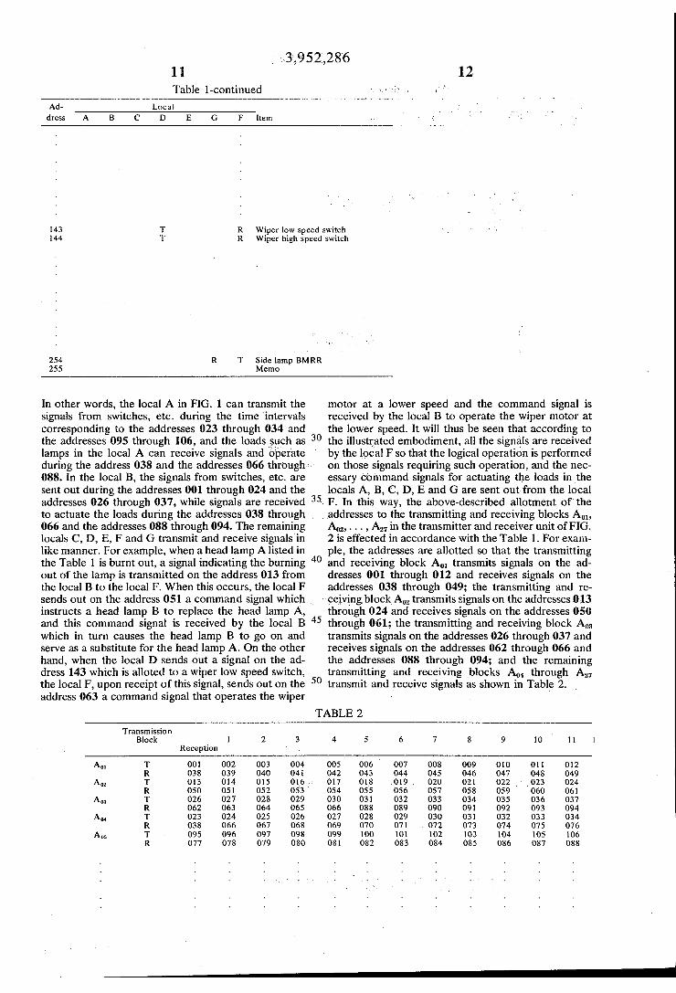
Table 1
Ad- Local dress A B C D E G F Item
000 001 T R Throttle position 2 002 T R Throttle position 4 003 T R Throttle position 6
012 T R 0l3 T R Headlamp A burnt out 014 T R Headlamp B burnt out
022 T R Faulty air bag 5 023 (T) T R Faulty air bag 6 024 T (T) R Front brake oil level 025 T R Rear brake oil level 026 T (T) R Front brake oil pressure 027 T (T) R‘ Rear brake oil pressure
3,952,286
Table l-continued Ad- Local dress B C D E G F Item
034 (T) (T) (T) (T) (T) R Faulty relays K,, L, 035 T (T) R Faulty relay K, 036 T T R R 037 T (T) (R) R 038 R (R) (R) (R) (R) T 039 R (R) T
049 R T 050 R T Actuate headlamp A 05] R T Actuate headlamp B 052 R T Actuate headlamp BM
061 R T 062 R T Actuate wiper motor at high
speed 063 R T Actuate wiper motor at low
’ speed 064 R T 065 R T 066 R T Actuate starter & ignition
coil 067 T Actuate solenoid AC
076 T Actuate headlamp F
088 R T R 089 R T R
094 (R) T R Failure to turn off key switch 095 R
106 (T) (R) (T) (T) R Front and rear tire pressures 107 (T) T (T) (T) R Headlamp dimmer
._ I 3,952,286
12 Table l-continued
Ad- Local dress A B C D E G F Item
143 T R Wiper low speed switch 144 T R Wiper high speed switch
254 R T Side lamp BMRR 255 Memo
In other words, the local A in FIG. 1 can transmit the signals from switches, etc. during the time 'intervals corresponding to the addresses 023 through 034 and the addresses 095 through 106, and the loads v‘such as lamps in the local A can receive signals and operate during the address 038 and the addresses 066 throughv 088. In the local B, the signals from switches, etc. are sent out during the addresses 001 through 024 and the addresses 026 through 037, while signals are received
30
to actuate the loads during the addresses 038 through‘ ; 066 and the addresses 088 through 094. The remaining locals C, D, E, F and G transmit and receive signals'in like manner. For example, when a head lamp A listed in the Table l is burnt out, a signal indicating the burning out of the lamp is transmitted on the address 013 from the local B to the local F. When this occurs, the local F sends out on the address 051 a command signal which instructs a head lamp B to replace the head lamp A, and this command signal is received by the local B which in turn causes the head lamp B to go on and serve as a substitute for the head lamp A. On the other hand, when the local D sends out a signal on the ad dress 143 which is alloted to a wiper low speed switch, the local F, upon receipt of this signal, sends out on the address 063 a command signal that operates the wiper
45
50
motor at a lower speed and the command signal is received by the local B to operate the wiper motor at the lower speed. It will thus be seen that according to the illustrated embodiment, all the signals are received by the local F so that the logical operation is performed on those signals requiring such operation, and the nec essary command signals for actuating the loads in the locals A, B, C, D, E and G are sent out from the local
= F. In this way, the above-described allotment of‘ the addressesto the transmitting and receiving blocks A01, A02, . . . , A27 in the transmitter and receiver unit of FIG. 2 is effected in accordance with the Table 1. For exam ple, the addresses are allotted so that the transmitting and receiving block Am transmits signals on the ad dresses 001 through 012 and receives signals on the addresses 038 through 049; the transmitting and re ceisvi'ngx block A02 transmits signals on the addresses0l3 through 024 and receives signals on the addresses 050 through 061; the transmitting and receiving block Ao3 transmits signals on the addresses 026 through 037 and receives signals on the addresses 062 through 066 and the addresses 088 through 094; and the remaining transmitting and receiving blocks A04 through A27 transmit and receive signals as shown in Table 2.
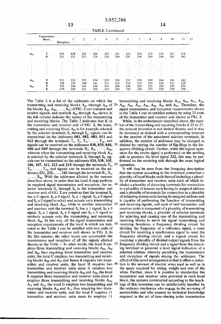
TABLE 2
Transmission Block 1 2 3 4 5 6 7 8 9 10 11
Reception '
A0, T 001 002 003 004 005 006 007 008 009 010 011 012 R 038 039 040 04 l 042 043 044 045 046 047 048 049
A0, T 013 014 015 01,6 017 018 .019 _ 020 021 022 023 024 R 050 051 052 '053 054 055 056 057 058 059 060 061
A03 T 026 027 028 029 030 031 032 033 034 035 036 037 R 062 063 064 065 066 088 089 090 091 092 093 094
AM T 023 024 025 026 027 028 029 030 031 032 O33 034 R 038 066 067 068 069 ()70 071 4 072 073 074 075 076
A05 T 095 096 097 O98 099 100 lot 102 KB 104 105 106 R 077 078 079 080 081 082 083 084 085 086 O87 O88
3,952,286
TABLE 2-continued
Transmission ‘ , ‘I \
Block 1’ 2 3v ' 4 5 6 7 8 9 10 l l 12 - l ' Reception - i -
A", T 034 038 f 1105 106 107 161 213 214 215 216 217 218 . R 231 232 233 234 . 235 . 236 237 238 239 240 241 242
A“ T‘ 231 232 ' '2'33 234' "235 236 237 3 232; 239 240 241 242 R 158 159 3160‘ \ 161 211V -212 "213 214 215 216 217 218
A25 T 243 244 , 245 246 247 248 249 250 ' 251 252 253 .254 R 219 220 221 222 224 225 22,6 227 228 229 230' 223
The Table 2 is a list of the addresses on which the transmitting and receiving blocks A0, through A25 of the blocks'Am, A02, . . ., A2‘, v‘0f_I~"IG'.'2 can transmitand receive signals, and symbols AQ1 through A25 shown, in the left column indicate the names of the transmitting and receiving blocks. The Table 2 indicates that if, in the transmitter and receiver unit of FIG. 2, the trans mitting and receiving block A01 is for example selected by the selector‘ terminals SLthrough S5,‘ signals can be transmitted onthe addresses 001,002, 003,011 and 012 through the terminals T1, T2, T3,", . . , Tu,‘ and signals can be received on the addresses 038,039, 040, 048' and 04'9Qthrough'the' terminals Rf, R2, . ,' Rl'z, whereas when the transmitting and receiving block A13 is selected by the selector‘ terminals S1 ‘through S5, sig nals can be transmitted on the addresses 034, 038, 105, 106, 107, 161, 213 and 218 through the terminals T1, T2, . . .’ , Th; and signals can be received on the ad dresses 231, ‘232, . , 242 through the terminals R1, R2, . .' . , R12. ‘With the addresses allotted in the manner
described above, in order that the local A may perform its required signal transmission and ‘reception, the se lector terminals Sl through S5 in the transmitter and receiver unit of FIG. 2 are preset so that the terminal 5, has a 0 signal, S, a 0 signal, S3 a" l signal,‘S4 a0 signal and S5 a 0 signal to select and actuate only transmitting and receiving block ‘A04, while in'another transmitter and receiver unit the'terminal S1‘; has a 1 signal,‘ S2 a 0 signal, S3~a 1 signal, S4a 0 signal and, S5 a 0 signal to similarly actuate only the‘ transmitting and receiving block A05. In this way, all the signal transmission and reception requirements of the local A‘ which are indi cated in the Table 1 can be satis?ed with two units of the transmitter and‘ receiver unit shown in FIG. 2.- In the like manner, the other locals can accomplishv the transmission and reception of all the signals allotted thereto in the Table 1. In other words, the local B em ploys three transmitting and receiving blocks A0,, A02 and A03 thus requiring three transmitter and receiver units, the local C employs two transmitting and receiv ing blocks A06 and A07 and hence it requires two trans mitter and receiver units, the local D requires two transmitter and receiver units since it employs two transmitting and receiving blocks A08 and A09, the local E requires three transmitter and receiver units since it employs three transmitting and receiving blocks Am, A" and Am, the local G employs two transmitting and receiving blocks A13 and A14 thus requiring two trans mitter and receiver units, and the local F requires 11 transmitter and receiver units since its employs l l
35
40
50
55
60
transmittingland receiving blocks A15, A16, A1,, A18, A19, A20, A2,, A22, A23, A2, and A25. Therefore, the signal transmission and reception requirements shown in the Table 1- can be satis?ed entirely by using 25 units of the transmitter and receiver unit shown in FIG. 2,. While, in the embodiment described above, the num
ber of the transmitting and receiving blocks is 25 or 27, the, present invention is not limited thereto and it may be increased as desired witha corresponding increase in the number of the associated selector terminals. In addition, the (number of addresses may be changed as desired by varying the number of ?ip-flops in thefre quency dividing circuit.- Further, while the logical oper ation for the strobe signal is performed on the sending side to produce the level signal 312, this may be per formed on the receiving side through the same logical operation.
It will thus be seen from the foregoing description that the system according to the invention comprises a plurality of local blocks each thereof including a plural ity of transmitter and receiver units each of which in cludes a plurality of detecting terminals for connection to a plurality of sensors each having its assigned address and a plurality of terminals for connection to a plurality of actuating means each having its assigned address ‘and is capable of performing. the function ofv transmitting and receiving signals, and each of said transmitter and receiver units is composed of a plurality of transmitting and receiving blocks, ‘a plurality of selector terminals for selecting and causing one of ‘the transmitting and receiving blocks to serve the signal transmittingand receiving functions, a frequency dividing circuit for dividing the. frequency, of a reference signal, a reset circuit for receiving. a synchronous signal to reset the frequency dividing circuit, and a logical circuit for receiving a plurality of divided output signals from the frequency dividing circuit and a signalfrom the detect ing terminal to generate a level signal indicative of a selected address, whereby permitting the transmission and reception of signals among the addresses. The effect of this novel arrangement is that it offers a reduc tion in the amount of electric wires used as well as in the space required for wiring, weight and cost of the wires. Further, since it is possible to standardize the transmitter and receiver units provided in each local block, the systems constructed according to the teach ings of this invention can be satisfactorily handled by the ordinary mechanics who engage in the servicing of automobiles and who possess no technical knowledge required in the art of time-sharing pulse transmission
3,952,286 15
system. Further, the number of terminals in the trans mitter and receiver unit which are connected to the sensors and the actuating means can be reduced to a minimum number corresponding to the number of addresses associated with the multiplex signal transmis sion and reception functions of a single transmitting and receiving block. What is claimed is: 1. An electric wiring system for interconnecting a
plurality of local blocks each thereof including a trans— mitter and receiver unit having transmitting and receiv ing functions and a plurality of terminals and a plurality of terminals means each thereof having an assigned address connected respectively to each of said termi nals, wherein at least one of said plurality of local blocks further includes oscillator means for generating a reference signal and means for generating a synchro nous signal having a period of desired cycle of said reference signal, and wherein each of said transmitter and receiver units includes a plurality of transmitting and receiving blocks commonly connected to said ter minals, a plurality of selector terminals for applying selecting signals to select one of said transmitting and receiving blocks corresponding to the assigned address of said terminal means and a counting block for receiv ing said synchronous signal and reference signal and for time-dividing each period of said synchronous signal by said reference signal to designate the address in order and for making the designated address agree with said assigned address and for applying said designated ad dress to said transmitting and receiving blocks, thereby accomplishing transmission and reception of signals among said local blocks corresponding to said assigned address by said transmitting and receiving blocks se lected by said selecting signals.
2. A system according to claim 1, wherein said tenni nal means comprises a plurality of sensors.
3. A system according to claim 1, wherein said termi nal means comprises a plurality of actuating means.
4. A system according to claim 1, wherein said select ing signals for selecting one of said transmitting and receiving blocks corresponding to the same speci?c address are added to a selector terminal of each trans mitter and receiver unit in ?rst and second local blocks, and a plurality of sensors are connected to the terminal means of said ?rst local block and a plurality of driving means are connected to the terminal means of said second local block, thereby each of said driving means corresponding to each speci?c address of said sensors is driven.
5. An electric wiring system for interconnecting a plurality of local blocks each thereof including a trans mitter and receiver unit, said transmitter and receiver unit including a plurality of detecting terminals respec tively connected to a plurality of sensors each having
5
20
25
35
16 an assigned address and a plurality of terminals respec tively connected to a plurality of actuating means each having an assigned address, each said transmitter and receiver unit serving signal transmitting and receiving functions, wherein at least one of said plurality of local blocks further includes oscillator means for generating a reference signal and means for generating a synchro nous signal, and wherein each said transmitter and receiver unit includes a plurality of transmitting and receiving blocks, a plurality of selector terminals for selecting and causing one of said plurality of transmit ting and receiving blocks to perform the signal trans mitting and receiving functions, a frequency dividing circuit for dividing the frequency of said reference signal, a reset circuit for receiving said synchronous signal to reset said frequency dividing circuit, and a logical circuit for receiving a plurality of frequency divided output signals of said frequency dividing circuit and a signal from one of said detecting terminals to generate a level signal designating a corresponding one said assigned addresses, whereby accomplishing the transmission and reception of signals among said as signed addresses. 5 s
6. A system according to claim 5, wherein each said transmitter and receiver unit includes a counting block for dividing the frequency of said reference signal for every period of said synchronous signal to generate an address signal corresponding to each of said addresses, a plurality of transmitting and receiving blocks adapted to received said address signal from said counting block and operatively associated with the signal transmitting and receiving functions of said plurality of local blocks, and a plurality of selector terminals for selecting and causing one of said plurality of transmitting and receiv
'ing blocks to effect a time-shared multiplex signal
40
45
50
55
60
65
transmission and reception according to said address signal, whereby to accomplish said signal transmission and reception among said addresses.
7. A system according to claim 5, wherein one of said plurality of local blocks further includes logical pro cessing means for receiving and performing a logical operation such as a check on a signal transmitted from each of said plurality of local blocks and sending back thereto a resultant command signal.
8. A system according to claim 5, wherein each of said transmitting and receiving blocks serves multiplex signal transmission and receiving functions involving a number of addresses corresponding to the number of said terminals connected to said plurality of sensors and actuating means.
9. A system according to claim 5, wherein said refer ence signal and said synchronous signal are respec tively transmitted along a separate transmission line.
* * * * *