Embed Size (px)
Citation preview
UNIVERSITÉ DE SHERBROOKE
Faculté de génie
Département de génie électrique et de génie informatique
ATTÉNUATION DES INTERACTIONS
ÉLECTROMAGNÉTIQUES ENTRE LE MODULE DE DÉTECTION
LABPET II ET L’IRM
MITIGATING ELECTROMAGNIC INTERACTIONS
BETWEEN LABPET II DETECTION MODULE AND MRI
SCANNERS
Thèse de doctorat
Spécialité : génie électrique
Narjes MOGHADAM
Sherbrooke (Québec) Canada
October 2019

ii
JURY MEMBERS
Réjean FONTAINE
Supervisor
Roger LECOMTE
Co-supervisor
Hamid Sabet
External examiner
Serge CHARLEBOIS
Examiner
Yves BÉRUBÉ-LAUZIÈRE
Examiner
iii
Résumé
Les scanners TEP/IRM simultanés offrent une occassion unique d'examiner en même
temps les propriétés anatomiques et fonctionnelles des tissus malins, tout en évitant
l'incertitude des systèmes séquentiels de TEP/IRM. Cependant, le couplage
électromagnétique entre les deux modalités constitue un défi important à relever. Ces
interférences électromagnétiques entravent les performances du scanner et altèrent la
qualité d'image de chaque modalité.
Bien que les métaux possèdent d'excellentes propriétés de blindage contre les
fréquences radioélectriques, ils ne constituent pas nécessairement une option de blindage
appropriée pour modifier les champs magnétiques induisant des courants de Foucault dans
les couches métalliques. En conséquence, il existe une demande considérable pour un
nouveau matériau de protection et une approche originale pour retirer les pièces métalliques
du champ de vision IRM.
L’objectif de ce projet était d’initier les études en vue de la réalisation d’un scanner
TEP/IRM simultané basé sur des modules de détection LabPET II hautement pixélisés afin
d’obtenir une résolution spatiale millimétrique pour le cerveau humain et le chien.
L'électronique LabPET II comprend des circuits intégrés à application spécifique dans
lesquels le signal est numérisé à proximité de la photodiode à avalanche et offre un
environnement moins sensible aux interférences électromagnétiques. Pour atteindre
l'objectif principal, premièrement, l'effet du matériau métallique des modules de détection
LabPET II sur les performances de la TEP et de l'IRM est examiné théoriquement. Les
résultats confirment que les composants métalliques du module de détection LabPET II
altèrent le champ magnétique, génèrent des courants de Foucault ce qui augmente leur
température. Ensuite, les performances électroniques des modules de détection LabPET II
sous l’influence de bobines d’IRM faites sur mesure sont examinées. La résolution en
énergie et la résolution temporelle se détériorent en présence de bobines RF et de bobines
à gradient en raison des perturbations électromagnétiques. Subséquemment, un module de
détection LabPET II blindé par une fine couche de composite cuivre-argent est étudié,
prouvant que le blindage contre les interférences électromagnétiques avec le composite
rétablit les performances en TEP, fournissant moins d'induction par courants de Foucault.
En outre, une nouvelle configuration de blindage basée sur un composite de couche flexible
de nanotubes de carbone a été fabriquée pour limiter les interférences électromagnétiques.
Les composites de nanotubes de carbone créent une couche hautement conductrice avec
des chemins conducteurs minimaux, ce qui permet de réduire les courants de Foucault.
Le principal résultat scientifique de ce projet est que le blindage composite empêche
les interférences de basses et hautes fréquences et réduit l'induction de courants de
Foucault, offrant ainsi la flexibilité nécessaire pour acquérir une séquence rapide de
commutation de gradients. D'un point de vue technique, le module de détection LabPET II
ainsi blindé présente une excellente performance dans un environnement de type IRM, ce
qui permet de concevoir un insert TEP basé sur la technologie LabPET II.
iv
Mots-clés: Tomographie d'émission par positrons (TEP), imagerie par résonance
magnétique (IRM), interférence électromagnetiquies, matériau composite à base de
nanotubes de carbone (CNT), blindage électromagnétique, courants de Foucault
v
Abstract
Simultaneous PET/ MRI scanners provide a unique opportunity to investigate
anatomical and functional properties of malignant tissues at the same time while avoiding
the uncertainty of a sequential PET/MRI systems. However, electromagnetic coupling
between the two modalities is a significant challenge that needs to be addressed. These
electromagnetic interferences (EMI) hinder the performance of both scanners and distort
the image quality of each modality.
Although metals have excellent radio-frequency shielding properties, they are not
necessarily an appropriate shielding option for altering magnetic fields that induce eddy
currents in any metallic layer. Thus, there is a considerable demand for a new shielding
material and an original approach to remove metallic parts from the MRI field of view.
The objective of this project was to initiate the realization of a simultaneous
PET/MRI scanner based on highly pixelated LabPET II detection modules to achieve
millimeter spatial resolution for the human brain and dogs. The LabPET II electronics
include application specific integrated circuits where the signal is digitized near the
avalanche photodiode and offers an environment less susceptible to EMI. To fulfill the
main aim, for the first time, the effect of the metallic material of LabPET II on PET and
MRI performance was theoretically examined. Results confirm that metallic components
of the LabPET II detection modules distort the magnetic field, generate eddy currents, and
increase temperature. Then, the LabPET II electronics performance under the influence of
custom-made MRI coils was investigated. Its energy and timing resolutions deteriorate in
the presence of both RF and gradient signals because of EMIs. Thus, a LabPET II detection
module shielded by a thin layer of the copper-silver composite was investigated, proving
that shielding EMIs with the composite restores the PET performance, with less eddy
current induction. Besides, a new shielding configuration based on a flexible layer of
carbon nanotube (CNT) composite was fabricated to limit the EMIs. The CNT composite
creates a highly conductive layer with minimal conductive paths that allows eddy currents
to be decreased.
The primary scientific outcome of this project is that the novel composite shielding
rejects both low and high-frequency interferences and reduces eddy current induction,
offering the flexibility to acquire a fast gradient switching sequence. From a technical point
of view, the shielded LabPET II detection module demonstrates an excellent performance
in an MRI-like environment supporting the feasibility of designing a PET-insert based on
LabPET II technology.
Keywords: Positron Emission Tomography (PET), Magnetic Resonance Imaging
(MRI), Electromagnetic Interferences (EMI), Carbon Nanotube (CNT); Composite,
Electromagnetic Shielding, Eddy Currents
vi
ACKNOWLEDGMENTS
The research presented in this dissertation is the result of a wide-ranging
collaboration. I am thankful to many people; not only for their contributions to scientific
knowledge but also for my personal benefit from the privilege of working alongside them.
The mentorship and guidance of these colleagues have been the best material from which
my graduate education has been advanced.
I would like to thank my advisor, Réjean Fontaine, and my co-advisor, Roger
Lecomte, for their advice, patience, mentoring, and support. It was a real privilege and an
honor for me to profit of their exceptional scientific knowledge but also their extraordinary
human qualities.
This project was realized with the great help, advice, and support of many of my
colleagues at Institut interdisciplinaire d'innovation technologique (3IT). I would
especially like to acknowledge the Groupe de Recherche en Appareillage Médical de
Sherbrooke (GRAMS) members at Université de Sherbrooke and Centre d'imagerie
moléculaire de Sherbrooke (CIMS) members from the research center of the CHUS. I have
learned a lot from you, and I will be forever grateful for it. Special thanks to Louis Arpin,
Romain Espagnet, Jonathan Bouchard, Nicolas Viscogliosi, Caroline Paulin, Konin Koua,
Haithem Bouziri, Catherine Pepin, Christian Thibaudeau, Jean-François Beaudoin, and
Luc Tremblay. I also would like to express my gratitude to my colleagues at Le laboratoire
de caractérisation et de synthèse des matériaux (LCSM) and Laboratoire Nanotechnologies
et Nanosystèmes (LN2), especially to Mohamed Walid Hassen, René Labrecque, Artur
Turala, and Pierre Langlois.
I acknowledge the financial support for my research study from the Quebec Bio-
Imaging Network (QBIN) and the Fonds de recherche du Québec – Nature et technologies
(FRQNT).
Finally, I am thankful to my parents, who have always encouraged and supported me
and lighten my way through all the steps I have taken. Many thanks to my best friend, Reza,
who has helped me to realize my dream and overcome all the challenging moments abroad.
vii
TABLE OF CONTENTS
Chapter 1 INTRODUCTION ................................................................................. 1
1.1. Context and Issues ..................................................................................... 1
1.2. Research Questions ................................................................................... 3
1.3. Objectives and Hypotheses of the Project ................................................. 4
1.4. Original Contributions and Thesis Layout ................................................ 7
Chapter 2 LITERATURE REVIEW .................................................................... 10
2.1. Fundamental Concept of PET ................................................................. 11
2.1.1. PET Components ................................................................................... 12
2.2. Overview of Magnetic Resonance Imaging ............................................ 13
2.2.1. MRI Parts............................................................................................... 14
2.2.2. Physics of MRI ...................................................................................... 15
2.3. Integrated PET and MRI ......................................................................... 16
2.4. Interaction between PET and MRI .......................................................... 20
2.4.1. Influence of PET on MRI ...................................................................... 21
2.4.2. Influence of MRI on PET ...................................................................... 23
2.5. PET/MRI Common Structure.................................................................. 29
2.6. Shielding .................................................................................................. 30
2.6.1. Shielding Effectiveness ......................................................................... 31
2.6.2. Shielding Materials for PET/MRI ......................................................... 32
2.7. Eddy Currents .......................................................................................... 40
2.8. Conventional Method to Measure the SE ............................................... 41
2.9. Fabrication of CNT Composites ............................................................. 43
Chapter 3 METALLIC MATERIAL EFFECTS .................................................. 49
Résumé en français .............................................................................................. 50
3.1. Introduction ............................................................................................. 53
3.2. Materials and Methods ............................................................................ 55
3.2.1. LabPET II Detector ............................................................................... 56
3.2.2. Field Inhomogeneity and Geometric Distortion Theory ....................... 58
3.2.3. Field Inhomogeneity .............................................................................. 59
3.2.4. Geometric Distortion ............................................................................. 60
3.3. Eddy Current and Heat Dissipation Simulation ...................................... 60
3.3.1. Effects of Position ................................................................................. 62
3.3.2. Experimental Test .................................................................................. 62
viii
3.4. Results ..................................................................................................... 63
3.4.1. Field Inhomogeneity .............................................................................. 63
3.4.2. Geometry Distortion Study .................................................................... 64
3.4.3. Eddy Current and Heat Dissipation Study............................................. 66
3.4.4. Effect of Position ................................................................................... 70
3.4.5. Experimental Results ............................................................................. 70
3.5. Discussion ............................................................................................... 71
3.6. Conclusion ............................................................................................... 73
Chapter 4 EFFECTS OF MRI COILS ON LABPET II PERFORMANCE: EMI
and shielding……… ......................................................................................................... 75
Résumé en français .............................................................................................. 76
4.1. Introduction ............................................................................................. 79
4.2. Materials and Methods ............................................................................ 82
4.2.1. LabPET II Building Blocks ................................................................... 82
4.2.2. LabPET II ASIC .................................................................................... 84
4.2.3. Energy And Timing Resolution Measurement Set Up .......................... 85
4.2.4. Choice of Shielding Material................................................................. 86
4.2.5. Mutual RF Interferences between the LabPET II and the RF Coil .... 87
4.2.6. Mutual Interferences between the LabPET II and the Gradient Coil . 90
4.3. Results ..................................................................................................... 91
4.3.1. Choice of Shielding Material................................................................. 91
4.3.2. Mutual RF Interferences between the LabPET II and the RF coil ..... 92
4.3.3. Mutual Interferences between the LabPET II and the Gradient Coil . 99
4.4. Discussion ............................................................................................. 104
4.5. Conclusion ............................................................................................. 107
4.6. Supplementary Information ................................................................... 109
Chapter 5 INTERPOSER: PERFORMANCE AND MODIFICATION ........... 112
Résumé en français ............................................................................................ 113
5.1. Introduction ........................................................................................... 114
5.2. Materials ................................................................................................ 117
5.3. Methods ...................................................................................................... 118
5.3.1. RF Coil Effects on the Interposer Detector ......................................... 119
5.3.2. Gradient Coil Effects on the Interposer Detector ............................. 120
5.3.3. Eliminating the Interferences ........................................................... 120
5.4. Results ................................................................................................... 121
ix
5.4.1. RF Coil Effects on the Interposer Detector ...................................... 121
5.4.2. Gradient Coil Effects on Interposer Detector ................................... 123
5.4.3. Eliminating Interferences ................................................................. 125
5.5 Discussion .................................................................................................... 127
5.6. Conclusion .................................................................................................. 128
5.7. Supplementary ....................................................................................... 129
Chapter 6 CNT-COMPOSITE SHIELDING ..................................................... 132
Résumé en français ............................................................................................ 133
6.1. Introduction ........................................................................................... 134
6.2. Materials and Methods .......................................................................... 138
6.2.1. Materials ........................................................................................... 138
6.2.2. Synthesize Process of Nano-Composite ........................................... 138
6.2.3. Nano-Composite Characterization ................................................... 139
6.2.4. LabPET II Performance Measurement ............................................. 140
6.3. Results and Discussion .......................................................................... 141
6.3.1. Nano-Composite Characterization ................................................... 142
6.3.2. LabPET II Performance .................................................................... 147
6.4. Conclusion ............................................................................................. 151
Chapter 7 Conclusion ......................................................................................... 154
7.1. Summary ............................................................................................... 154
7.2. Discussion ............................................................................................. 158
7.3. Contribution .......................................................................................... 161
7.4. Future work ........................................................................................... 164
7.5. French conclusion ....................................................................................... 166
Appendix A RF COIL DESIGN……………… ................................... 172
Steps for Designing of Surface Coil .............................................................. 172
Appendix B GRADIENT COIL ............................................................ 175
Appendix C Eddy CURRENT MEASUREMENT ............................... 177
REFERENCES .................................................................................................. 179
x
LIST OF FIGURES
Figure 1-1. Comparison of different biomedical imaging techniques. ...................... 2
Figure 2-1. The positron-emission decay process of an unstable nucleus. ............. 11
Figure 2-2. The non-collinearity effect on two scanners with different diameters. The
blue ring represents a smaller scanner and the gray one symbolizes a scanner with a larger
diameter. ............................................................................................................................ 12
Figure 2-3. The detection module (DM) of the LabPET II scanner. ...................... 13
Figure 2-4. A schematic of the main parts of an MRI. ............................................ 14
Figure 2-5. Schematic of three different methods to combine PET/MRI, (a)
sequential, (b) insert, and (c) fully integrated (Pichler et al., 2008a) ............................... 18
Figure 2-6. Comparison of simultaneous PET/MRI, PET/CT, and sequential
PET/MRI. (a) MRI, (b) simultaneous PET/MRI, (c) CT, (d) PET/CT, (e) MRI, and (f)
sequential PET/MRI (Richard et al., 2016). ..................................................................... 20
Figure 2-7. The effect of magnetic fields on the flood map of (a) a PMT and (b) an
APD (Pichler et al., 2008b). The 3D schemes of both detectors are also depicted. ......... 22
Figure 2-8.(a) flood map of PMT, (b) losing light pattern due to the presence of a
magnetic field, (c) adding materials with high magnetic susceptibility distorts main
magnetic field homogeneity (Pichler et al., 2008b). ......................................................... 24
Figure 2-9. The gradient ripple increases with the bias voltage (Düppenbecker et al.,
2016). ................................................................................................................................ 25
Figure 2-10. (a) Time jitter at the start of gradient pulse, (b) corresponding gradient
sequence (Düppenbecker et al., 2016). ............................................................................. 26
Figure 2-11. Effect of PET-insert on the noise level of the detected RF signal (Schulz
et al., 2011). ...................................................................................................................... 26
Figure 2-12. Mean ratios (with PET-insert divided by without PET-insert) of (a) SNR
and (b) homogeneity, calculated from 5 MRI acquisition sequencses for 17 slices. Values
on the right indicate the means of all slices (n=17); TSE: turbo spin echo, GE100 and GE
300: gradient-echo with a repetition time of TR=100, and TR=300 (Judenhofer et al.,
2008). ................................................................................................................................ 27
Figure 2-13. Mean ratios (inside MRI divided by outside MRI) of (a) single count
rates and (b) measured coincidence count rates, outside and inside the MRI during the
xi
acquisition of turbo spin-echo (TSE) and gradient-echo (GE) sequences (Judenhofer et al.,
2008). ................................................................................................................................ 28
Figure 2-14. (a) Light-fiber-based PET/MRI Systems, (b) short fiber and APD, (c)
modified magnet, (d) integrated PET/MRI (Vandenberghe and Marsden, 2015). ........... 29
Figure 2-15. SE as a function of the thickness of (a) a Cu plate for two different
frequencies, (b) a Cu mesh for various hole sizes for RF frequency of 100 MHz (Kang et
al., 2009). .......................................................................................................................... 32
Figure 2-16. Effect of an area of Cu plate on the MR image (Kang et al., 2009). .. 33
Figure 2-17. Chemical shift images (CSI) that give visual representations of induced
eddy current fields with no shielding present on the left, two different thicknesses of copper
shielding in the middle, and PET insert on the right (Peng et al., 2010). ......................... 33
Figure 2-18. (a) Gradient-echo sequence for different shielding configuration of
copper and (b) corresponding normalized error image (Peng et al., 2010). ..................... 34
Figure 2-19. Eddy current measurement using CSI for carbon fiber shielding with
two different delay times (a) t=0.0001 sec and (b) t=0.5 sec (Peng et al., 2014a). .......... 35
Figure 2-20. Shielding effectiveness vs. thickness for Cu plate, carbon fiber, and
MWNT composite at different frequencies. The SE of Cu mesh with two different hole
diameters for 3 T MRI is also displayed. .......................................................................... 36
Figure 2-21. (a) A typical electrical percolation of the CNT composite curve versus
aspect ratio. (b) The electrical conductivity of the functionalized SWNT- Reactive Ethylene
Terpolymer composites versus volume fraction of SWNT (Park et al., 2010). ................ 37
Figure 2-22. Shielding effectiveness of SWNT in epoxy resin (plot labeled A-D) and
MWNT composite (plot E-H) versus frequency (Li et al. 2006). ..................................... 38
Figure 2-23. SE of SWNT, comparison of different aspect ratios and the effect of
annealing (Li et al. 2006). ................................................................................................. 39
Figure 2-24. (a) the ASTM D4935-99 coaxial EMI SE tester; (b) required specimens
(ASTM, 1999). .................................................................................................................. 42
Figure 2-25. Illustrations, sizes, and photos of the newly developed SE tester
(Vasquez et al., 2009). ...................................................................................................... 42
xii
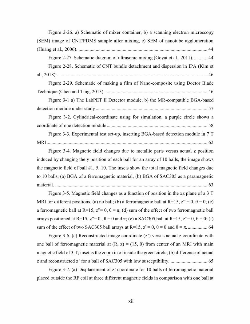
Figure 2-26. a) Schematic of mixer container, b) a scanning electron microscopy
(SEM) image of CNT/PDMS sample after mixing, c) SEM of nanotube agglomeration
(Huang et al., 2006). ......................................................................................................... 44
Figure 2-27. Schematic diagram of ultrasonic mixing (Goyat et al., 2011). ........... 44
Figure 2-28. Schematic of CNT bundle detachment and dispersion in IPA (Kim et
al., 2018). .......................................................................................................................... 46
Figure 2-29. Schematic of making a film of Nano-composite using Doctor Blade
Technique (Chen and Ting, 2013). ................................................................................... 46
Figure 3-1 a) The LabPET II Detector module, b) the MR-compatible BGA-based
detection module under study ........................................................................................... 57
Figure 3-2. Cylindrical-coordinate using for simulation, a purple circle shows a
coordinate of one detection module .................................................................................. 58
Figure 3-3. Experimental test set-up, inserting BGA-based detection module in 7 T
MRI ................................................................................................................................... 62
Figure 3-4. Magnetic field changes due to metallic parts versus actual z position
induced by changing the y position of each ball for an array of 10 balls, the image shows
the magnetic field of ball #1, 5, 10. The insets show the total magnetic field changes due
to 10 balls, (a) BGA of a ferromagnetic material, (b) BGA of SAC305 as a paramagnetic
material. ............................................................................................................................ 63
Figure 3-5. Magnetic field changes as a function of position in the xz plane of a 3 T
MRI for different positions, (a) no ball; (b) a ferromagnetic ball at R=15, z” = 0, θ = 0; (c)
a ferromagnetic ball at R=15, z”= 0, θ = π; (d) sum of the effect of two ferromagnetic ball
arrays positioned at R=15, z”= 0 , θ = 0 and π; (e) a SAC305 ball at R=15, z”= 0, θ = 0; (f)
sum of the effect of two SAC305 ball arrays at R=15, z”= 0, θ = 0 and θ = π. ................ 64
Figure 3-6. (a) Reconstructed image coordinate (z’) versus actual z coordinate with
one ball of ferromagnetic material at (R, z) = (15, 0) from center of an MRI with main
magnetic field of 3 T; inset is the zoom in of inside the green circle; (b) difference of actual
z and reconstructed z’ for a ball of SAC305 with low susceptibility. .............................. 65
Figure 3-7. (a) Displacement of z’ coordinate for 10 balls of ferromagnetic material
placed outside the RF coil at three different magnetic fields in comparison with one ball at
xiii
3 T; (b) change of z-z’ due to different gradient and magnetic field for ten SAC305 balls.
........................................................................................................................................... 66
Figure 3-8. Magnetic flux density of LabPET II detection module at (a) 10 kHz; (b)
100 kHz; Magnetic flux density zoom in at the ASIC edge at (c) 10 kHz; (d) 100 kHz; Heat
dissipation and induced eddy at (e) 10 kHz; (f) 100 kHz. Color bar: Volumetric heat
dissipation (W/m3). Streamline (red line): current density distribution, flashed blue lines:
magnetic flux density, flashed black lines: eddy current direction. .................................. 67
Figure 3-9. The magnetic flux density of a BGA-based detection module at (a) 10
kHz, (b) 100 kHz; Heat dissipation and induced eddy currents of a BGA-based detection
module at (c) 10 kHz and (d) 100 kHz; Color bar: Volumetric heat dissipation (W/m3).
Streamline (red line): current density distribution, arrow blue line: magnetic flux density.
........................................................................................................................................... 68
Figure 3-10. Eddy current and heat dissipation for BGA-based detection module at
(R, θ, z) = (15 cm, 9 degrees, 0) at (a) 10 kHz, (b) 100 kHz. Color bar: Volumetric heat
dissipation (W/m3). Streamline (red line): current density distribution. .......................... 70
Figure 3-11. Spin echo sequences image of a falcon tube filled with water in the
presence of (a) LabPET II module, (b) a BGA-based detection module inside the RF coil.
........................................................................................................................................... 71
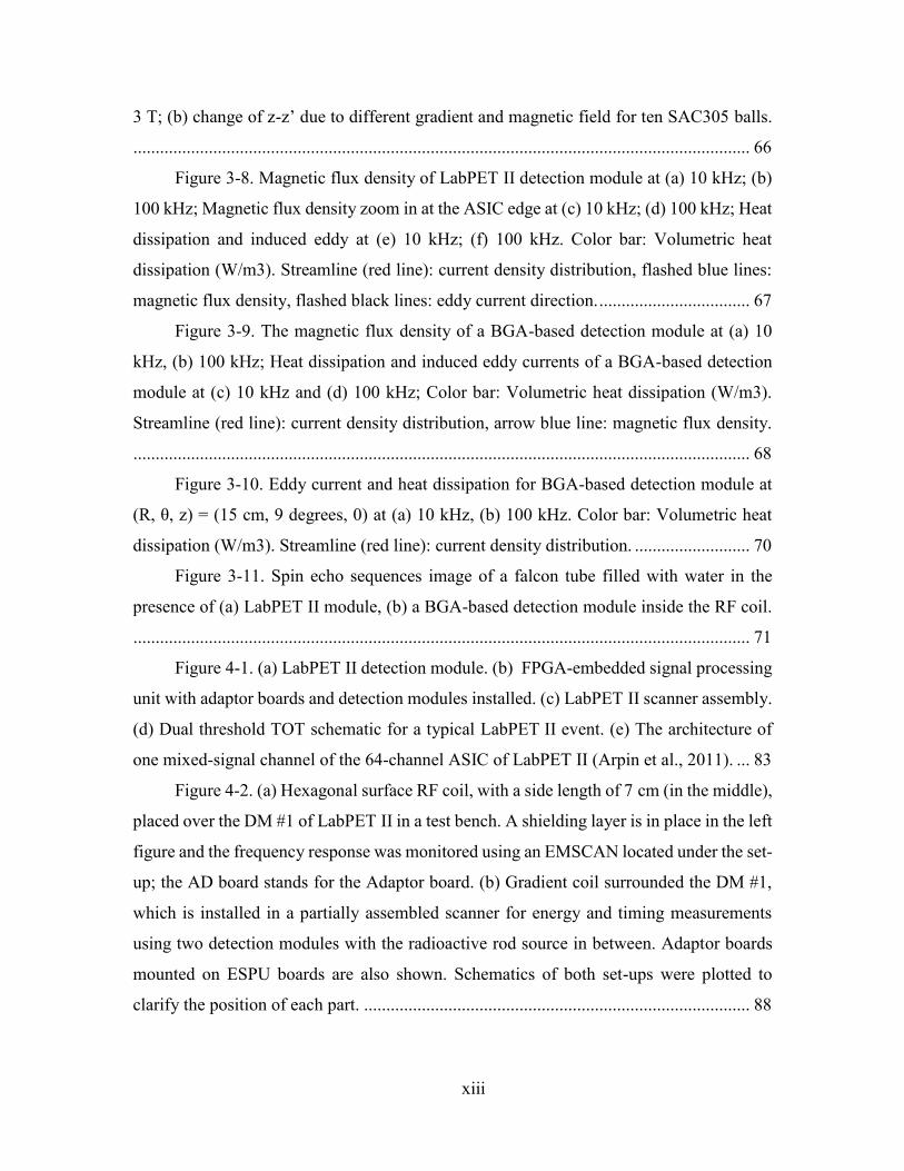
Figure 4-1. (a) LabPET II detection module. (b) FPGA-embedded signal processing
unit with adaptor boards and detection modules installed. (c) LabPET II scanner assembly.
(d) Dual threshold TOT schematic for a typical LabPET II event. (e) The architecture of
one mixed-signal channel of the 64-channel ASIC of LabPET II (Arpin et al., 2011). ... 83
Figure 4-2. (a) Hexagonal surface RF coil, with a side length of 7 cm (in the middle),
placed over the DM #1 of LabPET II in a test bench. A shielding layer is in place in the left
figure and the frequency response was monitored using an EMSCAN located under the set-
up; the AD board stands for the Adaptor board. (b) Gradient coil surrounded the DM #1,
which is installed in a partially assembled scanner for energy and timing measurements
using two detection modules with the radioactive rod source in between. Adaptor boards
mounted on ESPU boards are also shown. Schematics of both set-ups were plotted to
clarify the position of each part. ....................................................................................... 88
xiv
Figure 4-3. The normalized frequency response of signals received from LabPET II
electronic and RF coil at frequencies of (a) 127.74 MHz (3 T), (b) 298 MHz (7 T), and (c)
400.25 MHz (9.4 T). The 100 MHz, 300 MHz, and 400 MHz peaks correspond to the clock
signal, its 3rd and 4th harmonics. ....................................................................................... 93
Figure 4-4. RF coil effects on LabPET II detection modules: (a) baseline voltage and
(b) RMS noise level without RF coil emission (0 T) and with RF emission at 127.74 MHz
(3 T), 298 MHz (7 T) and 400.25 MHz (9.4 T). The pixels 1-128 belong to the DM #1
placed next to the RF coil and pixels 129-256 belong to the DM #2 located ~ 4 cm away
from the RF coil. The same legend is used for both figures. ............................................ 94
Figure 4-5. Histograms of the baseline for typical pixels from DM #1 exposed to the
RF signal of a 3 T system: (a) pixel 37, (b) pixel 92; and for a typical pixel from DM #2
away from 3 T coil: (c) pixel 137 of APD #1 of ASIC #1. ............................................... 95
Figure 4-6. a) The TOT energy spectra of one typical pixel without RF and with RF
signal at the three characteristic frequencies of 127.74 MHz, 298 MHz and 400.25 MHz
for 3 T, 7 T and 9.4 T. (b) Average coincidence time spectra of all coincident pixels
between two LabPET II modules without and with RF signal at the three characteristic
frequencies. The timing resolution for detection modules without RF signal (0 T) and the
worst case in the presence of the RF coil (7 T) were displayed in the figure, and all results
are reported in table 4-4. The energy and time spectra after fixing with the shielding layer
are also illustrated in the figures. ...................................................................................... 96
Figure 4-7. (a) The RMS noise level of all pixels of both detection modules working
at a clock rate of 100 MHz with and without shielding while exposed to RF emission at the
different MRI characteristic frequencies. (b) Noise level with a 106 MHz clock. DM #1
was at 1 mm away from the RF coil while DM #2 was about 4 cm away from the coil. . 98
Figure 4-8. The frequency response of the RF coil at (a) 127.74 MHz, (b) 298 MHz,
(c) 400.25 MHz with LabPET II’s clock working at 106 MHz. ....................................... 99
Figure 4-9. (a) Baseline voltage and (b) RMS noise level of all pixels of the
LabPET II detection modules in the presence of the gradient coil without and with gradient
switching at 10 kHz, 50 kHz and 100 kHz. DM #1 was inside the gradient coil and DM #2
was about 4 cm away from the coil. The same legend applies to both plots. ................. 100
xv
Figure 4-10. (a) The TOT energy spectra of a typical pixel of DM #1 without and
with 10 kHz, 50 kHz and 100 kHz gradient switching; (b) the energy resolution for all the
pixels in TOT bins without and with 10 kHz, 50 kHz and 100 kHz gradient; (c) coincidence
time spectra of the two detection modules without and with 10 kHz, 50 kHz and 100 kHz
gradient switching. The results for shielded DM #1 from the 100 kHz switching are shown
as a black dotted line. DM #1 was inside the gradient coil and DM #2 was about 4 cm away
from the coil. ................................................................................................................... 101
Figure 4-11. (a) Baseline voltage and (b) RMS noise level of the LabPET II detection
modules with and without gradient emission with the conductive paint used as a shielding
layer. The green dotted curve represents the case where the inside of the gradient coil was
covered by the conductive paint. The red dashed curve reports the case in which the DM
#1 was completely wrapped by the conductive paint. .................................................... 103
Figure 5-1. (a) Standard detection modules connected to the adaptor boards (AB), (b)
the same electronic modules as an interposer/carrier board, (c) backside of the carrier board
with four HV regulators, (d) front-side of the carrier board with four IDs, one with installed
crystal, two thermal pads can also be seen. .................................................................... 116
Figure 5-2. 3D view of Interposer detection module ............................................ 118
Figure 5-3. The gradient coil surrounded a detector installed on interposer board. A
standard Adaptor board (AB) is also displayed. ............................................................. 119
Figure 5-4. (a) The baseline and (b) the RMS noise level of two IDs in the presence
of RF coil signals. The inset of the figures (b) shows the noise of two standard DMs without
and with RF signals at 9.4 T (the worst case for standard DM). The same legend is used for
both figures and inset. ID #1 was 10 mm away from RF signals while ID #2 was 4 cm away
from RF coil. ................................................................................................................... 121
Figure 5-5. Baseline expansion of one pixel of the ID #1 in the presence of different
frequencies. ..................................................................................................................... 122
Figure 5-6. Gaussian fit of TOT energy spectrum of interposer detector (a) one
typical pixel of ID#1, (b) one typical pixel of ID#2; (c) energy resolution of all the pixels
of two modules, in the presence of different RF coil signals of 127.74 MHz (3T), 298 MHz
(7 T) and 400.25 MHz (9.4 T). ....................................................................................... 123
xvi
Figure 5-7. (a) Baseline, (b) RMS noise of the ID with and without gradient
switching. The inset of figure (b) shows the noise level of a standard DM without gradient
pulse and with gradient switching at 100 kHz. The legend is the same for both figures and
inset. ................................................................................................................................ 124
Figure 5-8. The TOT energy resolution of each pixel with and without gradient
switching. The inset shows the energy resolution of DM at the same conditions. ......... 125
Figure 5-9. Performance of the ID with shielding layer in the presence of RF signals
(a) RMS noise level of the ID, (b) Energy resolution of each pixel, inset is the fit of the
energy spectrum of one typical pixel at three Larmor frequencies. ................................ 126
Figure 5-10. Performance of the ID with shielding layer in the presence of the
gradient switching (a) RMS noise level of the ID, (b) Energy resolution of each pixel, inset
is the fit of the energy spectrum of one typical pixel. ..................................................... 127
Figure 6-1. Gradient coil is placed around the detection module #1 for energy and
timing measurement using two detectors. The radioactive rad has also been shown in the
figure. .............................................................................................................................. 141
Figure 6-2. Conductivity of (a) SWNT and (b) MWNT in different solvents using EIS.
UV-Vis spectra of (c) SWNT and (d) MWNT in IPA and Chloroform, (e) dispersion level
of SWNT and MWNT in the different solvents. ............................................................... 142
Figure 6-3. Conductivity versus frequency for SWCNT-IPA-PDMS composite with
2 wt. % and 10 wt.%. To provide EMI shielding, the impedances of material should be
more than the threshold level (green line), indicated in the figure ................................. 144
Figure 6-4. SEM of network generation of SWNT-PDMS with 2 kV energy and 20
µm aperture size, (a)the surface of 10 wt. % sample, (b) the fractured cross section of a 10
wt. % sample ................................................................................................................... 145
Figure 6-5. The coating of CNT composite over FR4 (10 wt.% CNT) in a shape of
the sample required for ASTM 4935-99 standard, left: load, right: reference ............... 145
Figure 6-6. Shielding effectiveness results using ASTM standard ....................... 146
Figure 6-7. a) Mean of baseline (b) RMS noise level for each pixel of one ASIC of
detection module in the presence of RF coil signal at 127.7 MHz (3T) and 298 MHz (7T).
The results for shielded module were also displayed. The legend for figures (a) and (b) is
the same. ......................................................................................................................... 147
xvii
Figure 6-8. (a) Gaussian fit of the energy spectra for one pixels, (b) Gaussian fit of
average energy spectra of one ASIC of LabPET II detection module (64 pixels) in the
presence of RF coil with CNT-composite as shielding layer. The results for shielded
module were also displayed. ........................................................................................... 148
Figure 6-9. Changes in baseline and noise level due to the gradient switching a)
without the gradient, b) gradient at 100 kHz, c) gradient at 100 kHz and shielding composite
in place. ........................................................................................................................... 149
Figure 6-10. Energy resolution for one module with and without gradient switching
and with shielding in place for 100 kHz gradient switching .......................................... 150
Figure 6-11. The temperature variation (difference between each case and the case
with fan without gradient switching) using different cooling configurations ................. 151
xviii
LIST OF TABLE
Table 2-1. Overview of PET/MRI system reported in the literature *(Disselhorst et
al., 2014). .......................................................................................................................... 17
Table 2-2. Interference effects of PET components on an MRI. ............................. 21
Table 2-3. The advantage (green) and disadvantage (red) of different detectors. ... 22
Table 2-4. Interference effects of MRI on PET performance. ................................ 24
Table 2-5. Pros and cons of different shielding approaches. ................................... 35
Table 2-6. Comparison of CNT, copper, and carbon fiber properties. .................... 37
Table 3-1. Susceptibility of different materials. ...................................................... 59
Table 3-2. Skin depth of copper and SAC305 at 100 kHz and 10 kHz ................... 61
Table 3-3. Net current and heat dissipation of a LabPET II detection module, BGA-
based detection module, and BGA-based detection module placed at the 0.5 mm distance
from the original one. ........................................................................................................ 69
Table 4-1. The shielding effectiveness of different materials at various frequencies,
for 1 mm copper or CHO-SHIELD, 3 mm of carbon fiber without Cu foil. The carbon fiber
SE values were presented based on the literature (Peng et al., 2014b, Greco et al., 2012)
........................................................................................................................................... 92
Table 4-2. Eddy current effects of copper, carbon fiber, and CHO-SHIELD® 2056
paint. .................................................................................................................................. 92
Table 4-3. Average difference of photopeak position from reference at 0 T and TOT
energy resolution for all pixels of APD#1 and APD#2 of ASIC #1 of DM#1 with and
without RF signals, with and without shielding. The negative sign means a lower bin. .. 95
Table 4-4. Time resolution with and without RF signals for the two detection modules
in coincidence, with and without shielding between the RF coil and detection modules. 97
Table 4-5. The average count rate of DM #1 (128 pixels) with and without shielding
in the presence of RF signals. ........................................................................................... 98
Table 4-6. The average count rate of DM #1 with and without shielding in the
presence of the gradient switching signals. ..................................................................... 102
Table 6-1. Eddy current induction on SWNT-PDMS layer with different
concentration ................................................................................................................... 147

xix
xx
List of Acronyms
ACRONYM DEFINITION
AB Adapter board
APD Avalanche photodiode
ASIC Application-specific integrated circuit
BGA Ball-grid array
CNT Carbon nanotube
CSA Chemical shift artifact
CSI Chemical shift image
DM Detection module
dTOT Dual time-over-threshold
EM Electromagnetic
EMI Electromagnetic interference
FOV Field of view
IPA Isopropyl alcohol
LDO Low-dropout
MRI Magnetic resonance imaging
MWNT Multi-wall carbon nanotube
PDMS Polydimethylsiloxane
PET Positron emission tomography
PSRR Power supply rejection ratio
RF Radio-frequency
SE Shielding effectiveness
SEM Scanning electron microscopy
SNR Signal to noise ratio
SWNT Single-wall carbon nanotube
TOT Time-over-threshold
UV-VIS Ultraviolet-visible

xxi
CHAPTER 1
INTRODUCTION
1.1. Context and Issues
Magnetic Resonance Imaging (MRI) is a conventional medical imaging modality
that records the magnetic field variations in a patient’s body. It has three main components.
Its first part is the main magnet that is generally made of superconducting magnets cooled
with Helium. It is crucial to preserve the magnetic field as homogeneously as possible. The
second part of an MRI includes three gradient coils, one for each direction, that provide a
linear gradation of the magnetic field. The third part is an RF coil, which transfers RF
energy at the Larmor frequency to align the nuclear spins of the Hydrogen atoms in the
body and receives the electromagnetic (EM) radiation from the precessing spins to produce
the image. The MRI scanner provides anatomical and functional images.
Another powerful and non-invasive method in medical imaging is Positron Emission
Tomography (PET). It involves the injection of a radiopharmaceutical into the body and
detection of the annihilation photons utilizing scintillation crystal arrays and a data
acquisition (DAQ) system. The PET scanner reveals the physiological information rather
than the anatomical data. The anatomical information is highly variable (from one image
to another one) and is generally absent in PET imaging. The major deficiency of a PET
scanner is its limitation to provide anatomical details due to its limited spatial resolution.
Precise localization of the lesions and improvement in the quantitative accuracy of the PET
signal is possible by providing anatomical information. The first approach to overcome this
deficiency is by using computer algorithms to co-register the PET images to those of
Computed Tomography (CT) or MRI (Levin et al., 1988). The second method to have
aligned anatomical and physiological images is to couple a PET acquisition system with
another anatomical imaging scanner and fabricate dual-modality scanners, for instance,
PET/CT or PET/MRI. Such dual-modality scanners, based on a combination of PET and
MRI, are classified into two types: (i) sequential PET/MRI and (ii) simultaneous PET/MRI.
Simultaneous PET/MRI scanners are capable of detecting the double amount of
information and of providing more biological and functional data than CT, without
2
increasing the radiation dose (Vandenberghe and Marsden, 2015). Thus, in comparison to
PET/CT, real simultaneous PET/MRI significantly reduces radiation exposure, lessens risk
and costs, and demonstrates safety and clinical values. Simultaneous PET/MRI also offers
soft-tissue contrast and motion correction. Besides, it could improve the spatial resolution
of the PET scanner using very high magnetic field MRI due to the reduction of the positron
range.
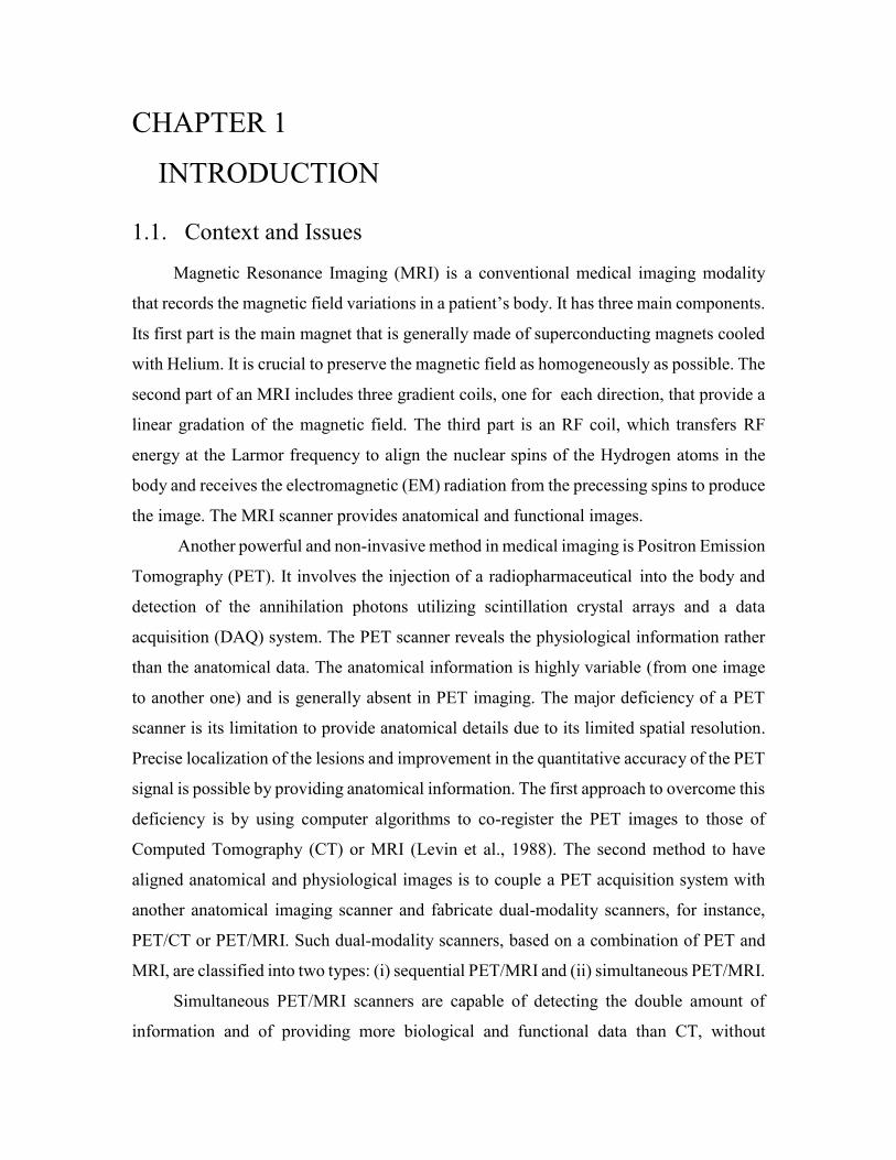
Figure 1-1 illustrates the comparison of different biomedical imaging methods. It
clearly shows that to have accurate and comprehensive results, radionuclide imaging
techniques must be combined with other functional or anatomical modalities.
Figure 1-1. Comparison of different biomedical imaging techniques.
However, integrating two electronic systems, such as PET and MRI scanners, causes
interactions between them that negatively affect each subsystem’s performance. There are
three crucial sources of interferences between PET and MRI; (i) radio frequency (RF) from
the MRI coil and PET clock; (ii) gradient switching frequency oscillating from 10 kHz to
100 kHz; (iii) the strong magnetic field of MRI with a typical range of 1.5 T to 9.4 T.
These interactions impose the use of an appropriate shielding configuration to avoid
mixing the RF signals, redesigning of the PET electronics to emit less electromagnetic
signals or the elimination of the problematic PET components from MRI field-of-view to
preserve the homogeneity.
Regardless of the technical challenges to combine PET and MRI into a single gantry,
there are two fundamentally different type of commercially available PET/MRI scanners.
The first one, from Siemens, was designed using an avalanche photodiode (APD)-based
PET scanner with 3 mm spatial resolution and 4 ns timing resolution. The second PET/MRI
scanner, from Philips, is a sequential one that shares a single patient handling system. It
enables spatially coordinated PET and MRI data to establish whole-body attenuation
correction. However, its lack of temporal matching between two functional datasets is an
intrinsic limitation. The improvement of the simultaneous approach taken by Siemens has
3
involved more academic works than the straightforward sequential approach retained by
Philips.
Advances in solid-state photodetectors and the use of APDs and silicon
photomultipliers (SiPM) open a new trend in PET/MRI scanners offering excellent timing
resolution. The LabPET II technology is a fully digital PET detection platform based on an
actual one-to-one coupling of crystals with APD pixels alongside independent parallel
processing. It uses a time-over-threshold scheme instead of pulse height analysis to allow
a high level of integration and to decrease power consumption.
Thus far, standard shielding configurations have used metallic materials, for
example, a plate and mesh of copper, which successfully have reduced electromagnetic
interferences (EMI) between PET and MRI; however, eddy current induction remains a
critical problem in this approach (Kang et al., 2009). Moreover, the metallic shielding is
expensive and heavy. Recently, researchers proposed to use carbon fiber to eliminate the
EMI from the RF coil and clock of PET and to decrease eddy current inductions.
Nevertheless, carbon fiber was unable to exclude EM interactions of the gradient switching
(Peng et al., 2014a).
On the other hand, recent research in high-frequency communication applications
using carbon nanotube (CNT) composites revealed their outstanding potential for perfect
electromagnetic shielding (Li et al., 2012). Using conductive composite based on carbon
nanotube instead of metal offers some particular advantages. First, it has a low atomic
number, thus, it is highly transparent to gamma radiation. Second, it has good electrical
and thermal conductivity. Third, producing carbon-based composite is significantly
cheaper than metal. Finally, it is very lightweight and flexible without the drawbacks of
metal such as corrosion and oxidation. Based on these unique characteristics, in this
project, carbon-based composites were considered as an attractive candidate for use in
simultaneous PET/MRI as a shielding material.
1.2. Research Questions
As the interferences between PET and MRI result from three different sources, the
main question is how to realize an MR-compatible PET-insert based on LabPET II
4
detection modules. This question requires examining material selection, EMI, shielding,
and temperature stabilization.
Magnetic field homogeneity is sensitive to the susceptibility of materials inserted
inside the MRI bore. Materials with different susceptibility than that of air causes
inhomogeneity and artifacts in MR images. Thus, for each part of the electronics of a PET-
insert, it is essential to know:
Could this material cause inhomogeneity?
What is the best alternative option for these components?
How could we change the electronic board design to decrease the inhomogeneity
of the main magnetic field or EMI?
Furthermore, the performance of LabPET II detection module under electromagnetic
distortion from MRI should be examined to answer the following questions:
What are the effects of the RF coils and the gradient coils at different frequencies
on the performance of the LabPET II detection module?
What are the shielding layer characteristics to minimize EMI between PET and
MRI scanners?
Besides, any varying magnetic field induces eddy currents on highly conductive
materials, resulting in increasing the temperature of electrical components of PET inserted
inside the MRI. Moreover, these currents generate another magnetic field in the opposite
direction of the gradient field that distorts the MR images. Thus far, to our knowledge,
none of the conventional shielding methods were capable of addressing, concurrently, all
issues associated with the gradient, namely low-frequency interferences, eddy currents, and
temperature stability. Consequently, our next bottleneck is:
How could we shield a PET scanner from EMI while reducing eddy currents and
stabilizing the temperature?
How can we increase the conductivity of a CNT composite in the low frequency?
What is the best method to fabricate a homogenous CNT-based composites?
1.3. Objectives and Hypotheses of the Project
Since the PET detection modules are located inside an intense static and dynamic
magnetic fields of MRI, the performance of both modalities may degrade. Our overall
5
objective is to make the LabPET II detection module compatible with an MRI scanner. In
this project, we focus on examining the performance of the LabPET II detection module in
the presence of gradient and RF coils, individually, and if needed on modifying the
detection module to develop an MR-compatible PET-insert.
The first goal of this thesis is to determine the effects of PET electronic components
on an MRI behavior while the metallic material is located between the RF coil and the
gradient coil of the MRI. The assumption is that ferromagnetic and conductive materials,
placed in an MRI bore, cause inhomogeneities in magnetic fields, which in turn generates
errors in an MR image. The effects of inserting ferromagnetic materials and the metallic
parts in the center of MRI have been mainly explored before (Costa et al., 2009, Shafiei et
al., 2003, Sasaki et al., 2013). However, the study of their effects outside the field of view
of MRI inside the gradient has never been explained. For the PET/MRI case, we need to
know which material parameters are important and how we can decrease the effects of
PET-insert electronics from a material point of view. To address these unanswered
concerns, we conducted two studies using theoretical calculations and COMSOL software
to examine the impacts of different susceptibility, conductivity and size of material on PET
and MRI in the presence of the magnetic field and the gradient switching. Furthermore, the
eddy current and heat dissipation were investigated.
The second goal of this project is to scrutinize the interferences between LabPET II
components and MRI parts with different magnetic strengths of 3 T, 7 T and 9.4 T. In fact,
the objective is to identify the most vulnerable components of LabPET II electronics when
an MRI is turned on. If the performance of LabPET II detection module is acceptable, we
could conclude that it is safe to insert the LabPET II electronics inside an MRI. For this
reason, the analog baseline voltage, RMS noise level, energy, and timing resolutions of the
LabPET II detection module were acquired in the presence of gradient and RF coil signals
and the results were compared with the LabPET II detection module results without EM
interferences. The results of this very first experiment of the LabPET II detection module
in the presence of EMI showed changes in PET performance that need to be addressed.
The third goal of this thesis is to reduce the interferences between LabPET II and
MRI scanners using a suitable shielding configuration or redesigning PET electronics. The
hypothesis is that a specified thickness of any conductive layer shields the electromagnetic
6
frequency. Thus, for a well-defined frequency of the RF coil, an appropriate thickness of
conductive material was calculated based on the material conductivity. Consequently, to
eliminate the observed effects, the LabPET II detection module was shielded from EMI
sources using specific thickness based on the material properties. Then the PET
performance was measured to determine the effectiveness of the shielding layer in
improving the PET performance.
The fourth goal of this project is to eliminate the effects of eddy currents due to the
gradient switching on PET-insert and MRI; hence, we need to find a shielding material that
generates fewer eddy currents than a metallic layer while blocking the low-frequency RF
emission from the MRI. The hypothesis was that a conductive composite with a good
conductivity could eliminate the RF interaction. Besides, a conductive composite has a
network-shaped conductive structure and it is composed of small conductive loops. Thus,
it only creates insignificant quantities of eddy currents. Furthermore, each layer of a
composite material could compensate for the eddy current effects of the adjacent layer, as
if it was composed of multi-laminated layers. Therefore, it has less negative influences on
MRI image quality. Taking advantage of carbon nanotube composites, a new flexible
shielding configuration able to eliminate eddy current effects was proposed.
The next goal is to examine whether a new design of LabPET II front-end (called
interposer) considering a change of components size and removing ferromagnetic parts
could improve PET-insert performance in the presence of MRI coils. The hypothesis was
that sandwiching an ASIC between two printed circuits boards (PCB) can make it immune
to EMI. The obtained results confirm less interaction between PET and MRI signals in
comparison with a standard LabPET II detection module; however, the results also show a
noticeable change in the performance of the interposer detector such as its noise level and
energy resolution.
The last goal was to investigate the effects of the LabPET II electronics on an RF
signals of MRI. The hypothesis was that as the PET electronics were placed near the RF
coil, the PET electronics would deteriorate the RF signal if the clock harmonics fell within
the RF coil bandwidth. Since our goal is to design PET electronics working at different
magnetic fields of MRI, the RF coil signal in the presence of a 100 MHz PET’s clock was
7
measured. Afterwards, we proposed to change the PET clock in a way that its harmonics
were removed from all three bandwidths of the MRI RF coil.
1.4. Original Contributions and Thesis Layout
The aformentioned questions in section 1.2 are answered through the four published
and submitted papers. The chapters of this report are organized in a way to clearly address
the challenges of genuinely simultaneous PET/MRI scanners using the LabPET II
technology and to describe the methods to overcome those issues. The effects of material
properties on the PET and MRI behavior are presented. The relative performance of the
LabPET II detection module with and without MRI coils is evaluated. Specific approaches
to eliminate those problems have been employed and their influences on the PET
performance have been described. Finally, fabrication of a new shielding material and the
obtained results using this shielding are described.
This document will be followed by a review of the state-of-the-art in chapter 2 where
the PET scanner, MRI scanner, and challenges in front of bimodal scanners as well as the
means to overcome them with emphasis on shielding methods are explained. Chapter 3
includes the paper entitled “Studying the Effects of Metallic Components of PET-insert on
PET and MRI Performance due to Gradient Switching” published in Physics in Medicine
and Biology, 2019; 64 (7), which focuses on the metallic material effects on PET and MRI
performance because of the gradient switching. The goal is to find out whether inserting
metallic parts outside the imaging field of view of MRI scanner, between the gradient and
the RF coils, would disturb the MRI performance or even the PET performance. The results
confirm that the ferromagnetic parts interact with the performance of both scanners and
should be eliminated from the MRI gantry. In this chapter, we also discuss the essential
design consideration to have an MR-compatible PET detection module. In chapter 4, we
present a paper entitled “Initial MR-Compatibility Investigation of LabPET II Detector
Technology for Simultaneous PET/MRI” submitted to Physics in Medicine and Biology.
This paper describes the results of placing the LabPET II detection module in a situation
similar to that of an MRI bore. The effects of the gradient and RF coils on the PET
performance are determined, and appropriate methods to minimize those effects are
presented. In chapter 5, the third paper, with the title “MRI-Compatibility Study of a Low-
8
Profile Positron Emission Tomography Front End with Submillimeter Resolution”, in
preparation for submission to Nuclear Instruments and Methods in Physics Research
Section A, is presented. The performance of interposer detector, as a modified version of
the LabPET II detection module, in the presence of EMI is investigated. A composite layer
is applied to eliminate the EMI remaining after sandwiching ASICs between two electronic
boards. Chapter 6 includes the last paper entitled “Shielding Electromagnetic Interference
of Simultaneous PET/MRI Using Flexible Ultra-Thin Carbon-Nanotube Composite”
prepared to be submitted to IEEE Transactions on Nanotechnology. It discusses the
fabrication of new shielding composite based on CNT and clarifies how it could improve
PET/MRI performance. Different solvents were examined to synthesize a composite with
high conductivity at the desired frequency range. Chapter 7 provides a summary and
conclusion on this project and justifies future designs and tests required for developing the
LabPET II-based detection module to be compatible with MRI. In appendix A to C, the
RF coil and the gradient coil design considerations, as well as the eddy-current
measurement set-up, are described, respectively.

9
10
CHAPTER 2
LITERATURE REVIEW
The first idea of a hybrid PET and MRI originates back to 1986 when Iida proposed
employing a magnetic field to enhance the spatial resolution of PET (Iida et al., 1986).
However, the first hybrid PET/MRI, introduced in 1997, consisted of a single ring PET
scanner mounted within the RF coil of the MR scanner (Yiping et al., 1997), while
SPECT/CT had been already used in clinical applications (Hasegawa et al., 1990). The first
drawback of a PET/MRI hybrid was the susceptibility of the photomultiplier tubes (PMT)
detector of the PET scanner to the magnetic interferences. The initial designs utilized
optical fiber cables to transfer the light from crystals to the PMT detectors located outside
the strong static magnetic field of the MRI. The first pre-clinical PET/MRI scanner with a
1.5 T magnetic field was developed using this approach in 2006 (Catana et al., 2006, Lucas
et al., 2006). The second approach employed a split magnets (Shaw et al., 2005) beween
which the PET scanner was inserted, but maintenaning the magnetic field’s homogeneity
was more difficult than with the standard structure.
By developing non-magnetic sensitive silicon-based photodetectors for PET such as
APD- (Lecomte et al., 1993) and SiPM- (Renker, 2006) based scanners, the combination
of these two modalities to acquire data simultaneously turned to become possibile. A
prototype integrated LSO-APD-based PET scanner and 7 T MRI for small animal
applications was developed in 2006 (Pichler et al., 2006). Furthermore, a fast SiPM-based
PET device has been inserted in 3 T MR for pre-clinical usage (Schulz et al., 2011, Weissler
et al., 2012). The first human PET/MRI scanners constructed by Siemens consisted of a
head BrainPET scanner and a modified 3 T MAGNETOM Tim Trio as MRI (Schlemmer
et al., 2008). Moreover, the sequential PET/MRI scanner called the Philips Ingenuity TF
(Herzog and Van den Holf 2012) and the simultaneous PET/MRI of Siemens (Zaidi and
Del Guerra, 2011) has been implemented for whole-body applications. Recently, GE has
integrated time-of-flight PET with 3 T MRI for whole-body use. The principal goal, which
has been pursued in all the above-mentioned methods, is to minimize the coupling between
11
two subsystems and preserve the performance of each modality. Currently, the
development of a hybrid PET/MRI is an active field of research.
2.1. Fundamental Concept of PET
PET involves the injection of a radiopharmaceutical into the patient’s body. The
radiolabeled compound is known as a tracer or radiotracer. While the positron-
emittingradioisotope decays, two annihilation photons with energy equal to the rest-mass
energy of an electron or a positron, i.e. 511 keV, are emitted and detected by a ring of
detectors (Cherry et al., 2010).
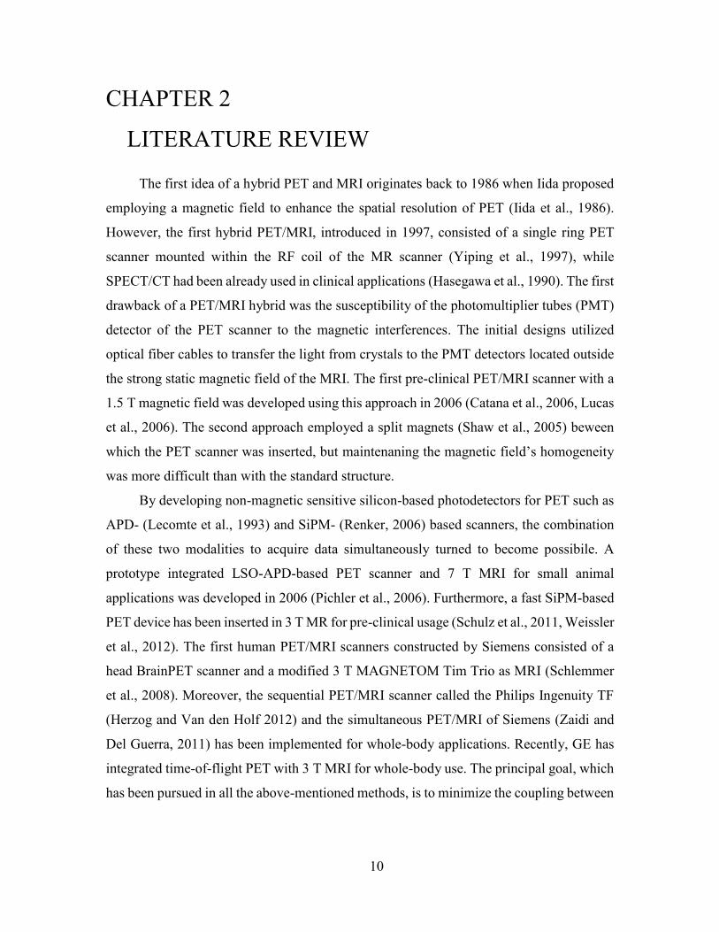
Indeed, the positron and electron form a momentary atom and then the positron
combines with the electron and emits two annihilation photons, which leave the
annihilation event site in nearly opposite directions (Figure 2-1). Nevertheless, due to the
kinetic energy of both particles, the annihilation photons may be emitted non-collinearly
(about 0.25o deviation) which affects the ability of positron localization.
Figure 2-1. The positron-emission decay process of an unstable nucleus.
The average positron range is important for determining the spatial resolution since
the annihilation sites are far away from the transformation sites (in quantum physics scale)
owing to the positron range. It is worth mentioning that applying a strong external magnetic
field evidently improves spatial resolution when the positron possesses high energy. Thus,
an ultra-high field PET/MRI has the potential to improve the spatial resolution of a PET
image in planes perpendicular to the main magnetic field because of the confinement of
the positron range (Hammer et al., 1994).
12
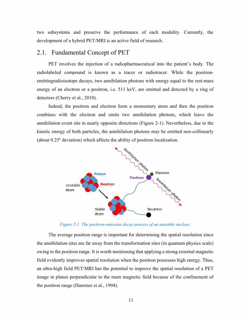
The non-collinearity becomes vital in a large diameter scanner such as a brain
scanner or whole-body scanner, where, the probability of detecting slightly misplaced
events increase as shown in Figure 2-2. Therefore, in a large diameter scanner, it is
plausible to identify the activity by the adjacent crystals due to a slight change in the
positron direction or a small deviation of the angle, especially when a thin crystal is
implemented in the PET detector.
Figure 2-2. The non-collinearity effect on two scanners with different diameters. The blue ring
represents a smaller scanner and the gray one symbolizes a scanner with a larger diameter.
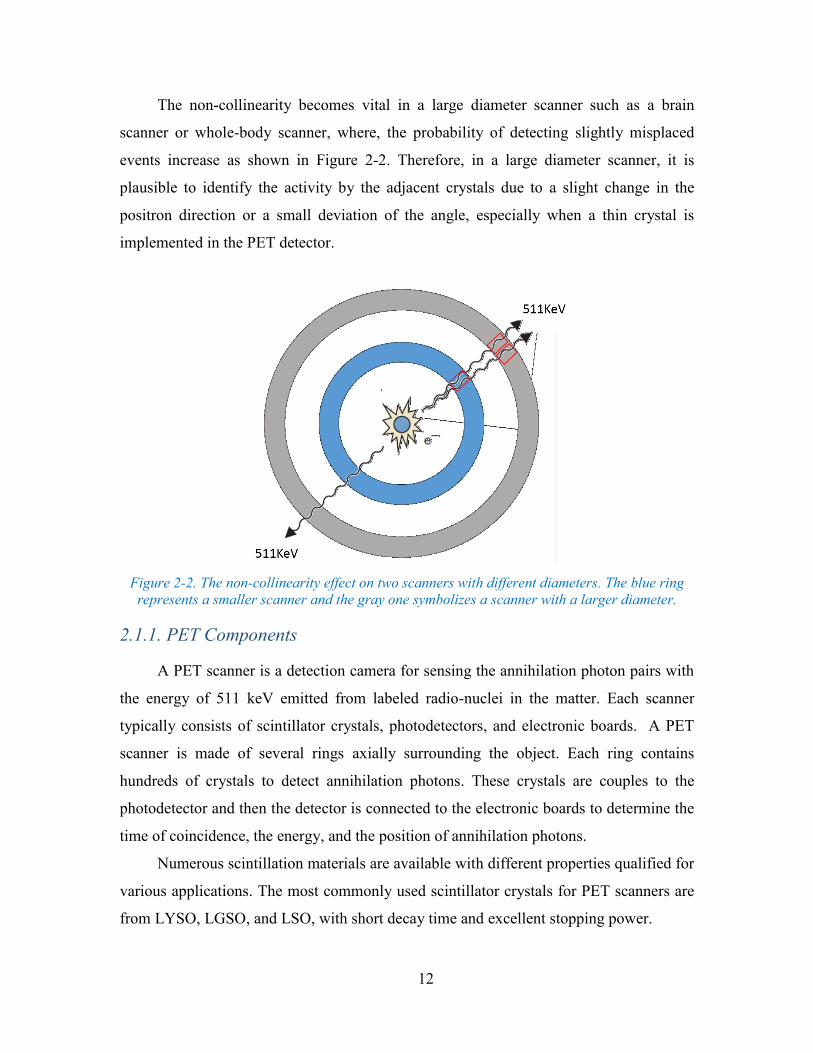
2.1.1. PET Components
A PET scanner is a detection camera for sensing the annihilation photon pairs with
the energy of 511 keV emitted from labeled radio-nuclei in the matter. Each scanner
typically consists of scintillator crystals, photodetectors, and electronic boards. A PET
scanner is made of several rings axially surrounding the object. Each ring contains
hundreds of crystals to detect annihilation photons. These crystals are couples to the
photodetector and then the detector is connected to the electronic boards to determine the
time of coincidence, the energy, and the position of annihilation photons.
Numerous scintillation materials are available with different properties qualified for
various applications. The most commonly used scintillator crystals for PET scanners are
from LYSO, LGSO, and LSO, with short decay time and excellent stopping power.
13
The PMT was undoubtedly the most widely used photodetector in PET. However,
new challenges, such as the reduction of a PET scanner’s diameter and implementation of
PET/MRI scanners, motivated researchers to consider other types of detectors. The APD
has been used in commercial scanners (Lecomte et al., 2006) and the SiPMs (Llosa et al.,
2008) and single-photon avalanche diode (SPAD) (Renker, 2007, Cova et al., 1996,
Piemonte, 2006, Dolgoshein et al., 2006) are currently under investigation.
The LabPET II is a small animal PET scanner designed and developed at Université
de Sherbrooke with sub-millimeter spatial resolution. The detection module of the
LabPET II, shown in Figure 2-3, includes four parts:
(i) Scintillation crystals convert high energy annihilation photons into visible
photons.
(ii) Avalanche photodetectors detect and convert these photons into an electrical
signal, which is used by electronic boards for further processing.
(iii) Application-specific integrated circuits (ASICs) amplify and shape the APD
signal to extract the relevant information such as time and energy of the
detected photons.
(iv) A connector transfers digital signals to the acquisition electronics.
Figure 2-3. The detection module (DM) of the LabPET II scanner.
2.2. Overview of Magnetic Resonance Imaging
The world's first MRI scanner was invented in the 1970s. At that time, Damadian
proposed using Nuclear Magnetic Resonance (NMR) signal to form images of issues
14
withen the body (Damadian, 1974) and Lauterbur reported the first application of Magnetic
Resonance Imaging (MRI) (Lauterbur, 1973). In 1974, Lauterbur and Mansfield, without
knowledge of each other’s work, described the use of magnetic field gradients for spatial
localization of NMR signals. Their discoveries established the foundation of MRI.
Primary MR imaging was time-consuming and challenging. Modern scanners
provide images with different contrast of objects in vivo. The capability of MRI to acquire
anatomical images with high spatial resolution and superior soft-tissue contrast, along with
revealing information of perfusion, diffusion, and local chemical composition of tissue,
made it one of the most valuable imaging modalities.
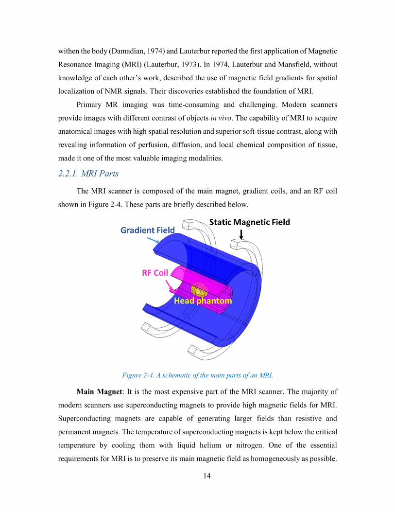
2.2.1. MRI Parts
The MRI scanner is composed of the main magnet, gradient coils, and an RF coil
shown in Figure 2-4. These parts are briefly described below.
Figure 2-4. A schematic of the main parts of an MRI.
Main Magnet: It is the most expensive part of the MRI scanner. The majority of
modern scanners use superconducting magnets to provide high magnetic fields for MRI.
Superconducting magnets are capable of generating larger fields than resistive and
permanent magnets. The temperature of superconducting magnets is kept below the critical
temperature by cooling them with liquid helium or nitrogen. One of the essential
requirements for MRI is to preserve its main magnetic field as homogeneously as possible.
15
A magnetic field homogeneity lower than 1 p.p.m. over the volume of interest is
acceptable.
Gradient Coils: The gradient coils generate the secondary magnetic fields. They are
located inside the MRI gantry and arranged in the opposite direction to produce a negative
and positive pulse. There are three gradient coils, one for each axis, that produce linear
gradations of the the magnetic field to enable localization of MR signals in the x, y, z
directions. Once they are switched on, one side of the magnet bore has lesser strength and
the other side has greater strength than the main static magnetic field. This variation permits
the localization of image slices that is necessary to form MR images.
RF Coil: The RF coil is a transmitter/receiver that broadcasts the RF signal to the
patient and receives the returned signal. A radio frequency pulse with a frequency equal to
the Larmor frequency of hydrogen atoms is emitted from an RF coil to align the phase and
tip over the nuclei that causes decrement in the longitudinal magnetization and establishes
a new transversal one.
2.2.2. Physics of MRI
MRI is one of the most commonly used medical imaging methods, which records the
RF signal emitted from atoms excited at their Larmor frequency. One key advantage of
MRI is that allows the accurate measurement of anatomical data without injecting
radiopharmaceuticals.
The physics of MRI is entirely different from the PET and CT princibles. In MRI,
the image of tissue is generated by transverse magnetization precesses at Larmor
frequency, which induce a current in an RF coil. These signals were generated in the body
by protons as a response to the trigger from the radiofrequency pulses.
The human body is mainly composed of water (50-75%) and fat (20-30%), both
containing hydrogen atoms. MRI detects the presence of hydrogen atoms using a strong
magnetic field. Thus, MRI creates images by exciting the hydrogen spins to their higher
energy level; then their magnetization is tilted to the transverse plane by a tuned RF coil.
This magnetization induces eddy currents in the RF coil. The frequency of the RF signal is
proportional to the magnetic field to which these atoms are subjected during the relaxation
process and is defined by the Larmor equation as (Mackiewich, 1995, Nishimura, 2010):
16
B 0 (2.1)
where ω0 is known as either the precessional, Larmor or resonance frequency, B is the main
magnetic field, and γ is the gyromagnetic ratio that is a unique constant of every atom. The
gyromagnetic ratio of a proton (Hydrogen) is 42.58 MHz/Tesla.
When a strong magnetic field is applied to the body, many of the free hydrogen nuclei
align parallel or anti-parallel to the magnetic field. The aligned atoms create the magnetic
moments M paralleled to the main magnet, the sum of these moments creates the net
longitudinal magnetization (ML). Since ML is parallel with B, it is not possible to detect it.
To change the magnetization direction, an RF pulse is triggered at the corresponding
Larmor frequency to rotate the ML by 90 degrees. In this situation, all the ML vectors cancel
each other out and the transverse magnetization (MT) of atoms, which rotates with the
frequency of ω, can be detected as a dynamic magnetization. According to Faraday’s law,
this magnetic variation induces a voltage in the receiver coil. By turning off the RF signal,
the transverse magnetization starts to disappear and the longitudinal magnetization raises
to its original value. The detected signals by an RF receiving coil originate from the entire
body and the generated image excludes any spatial encoding information. Therefore, the
gradient coils are used to locate the origin of a signal by slice selection, frequency
encoding, and phase encoding depending on the position of targeted tissue (Lipton, 2008).
2.3. Integrated PET and MRI
Several reasons make PET/MRI an appropriate scanner for clinical and preclinical
studies. First, large varieties of PET tracers are available and the sensitivity of PET is in
the pico-molar range. Second, MR delivers high resolution and high soft-tissue contrast
images in comparison with other molecular imaging modalities. Third, the PET image can
be complemented by the MR image. From another point of view, simultaneous imaging of
PET and MRI could save total acquisition time and create images with multiple dynamic
processes. Besides, MRI can be used to correct motion in PET data. Lastly, there is no need
to inject an additional radiation dose for MR images. PET/MRI overcomes some of the
limitations of PET/CT such as limited soft-tissue contrast and high radiation doses. In
PET/CT scanners, while both systems share a common patient bed, they are hard-wired
back-to-back thus impeding simultaneous data acquisition, which is possible to achieve
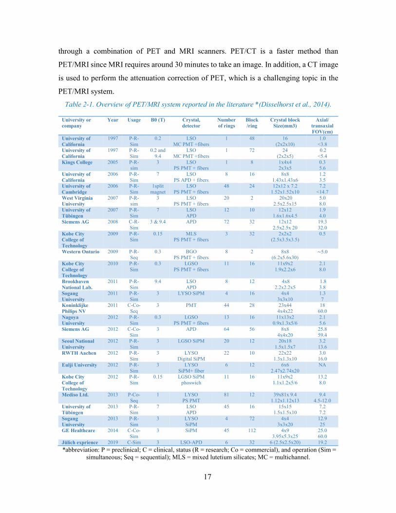
17
through a combination of PET and MRI scanners. PET/CT is a faster method than
PET/MRI since MRI requires around 30 minutes to take an image. In addition, a CT image
is used to perform the attenuation correction of PET, which is a challenging topic in the
PET/MRI system.
Table 2-1. Overview of PET/MRI system reported in the literature *(Disselhorst et al., 2014).
University or
company
Year Usage B0 (T) Crystal,
detector
Number
of rings
Block
/ring
Crystal block
Size(mm3)
Axial/
transaxial
FOV(cm)
University of
California
1997 P-R-
Sim
0.2 LSO
MC PMT +fibers
1 48 16
(2x2x10)
1.0
<3.8
University of
California
1997 P-R-
Sim
0.2 and
9.4
LSO
MC PMT +fibers
1 72 24
(2x2x5)
0.2
<5.4
Kings College 2005 P-R-sim
3 LSO PS PMT + fibers
1 8 1x4x4 2x3x5
0.3 5.6
University of
California
2006 P-R-
Sim
7 LSO
PS APD + fibers
8 16 8x8
1.43x1.43x6
1.2
3.5
University of
Cambridge
2006 P-R-
Sim
1split
magnet
LSO
PS PMT + fibers
48 24 12x12 x 7.2
1.52x1.52x10
7.2
<14.7
West Virginia
University
2007 P-R-sim
3 LSO PS PMT + fibers
20 2 20x20 2.5x2.5x15
5.0 8.0
University of
Tübingen
2007 P-R-
Sim
7 LSO
APD
12 10 12x12
1.6x1.6x4.5
1.9
4.0
Siemens AG 2008 C-R-
Sim
3 & 9.4 APD 72 32 12x12
2.5x2.5x 20
19.3
32.0
Kobe City
College of
Technology
2009 P-R-Sim
0.15 MLS PS PMT + fibers
3 32 2x2x2 (2.5x3.5x3.5)
0.5
Western Ontario 2009 P-R-Seq
0.3 BGO PS PMT + fibers
8 2 8x8 (6.2x5.6x30)
∼5.0
Kobe City
College of
Technology
2010 P-R-
Sim
0.3 LGSO
PS PMT + fibers
11 16 11x9x2
1.9x2.2x6
2.1
8.0
Brookhaven
National Lab.
2011 P-R-
Sim
9.4 LSO
APD
8 12 4x8
2.2x2.2x5
1.8
3.8
Sogang
University
2011 P-R-
Sim
3 LYSO SiPM 4 16 4x4
3x3x10
1.3
7
Koninklijke
Philips NV
2011 C-Co-
Seq
3 PMT 44 28 23x44
4x4x22
18
60.0
Nagoya
University
2012 P-R-
Sim
0.3 LGSO
PS PMT + fibers
13 16 11x13x2
0.9x1.3x5/6
2.1
5.6
Siemens AG 2012 C-Co-
Sim
3 APD 64 56 8x8
4x4x20
25.8
59.4
Seoul National
University
2012 P-R-
Sim
3 LGSO SiPM 20 12 20x18
1.5x1.5x7
3.2
13.6
RWTH Aachen 2012 P-R-Sim
3 LYSO Digital SiPM
22 10 22x22 1.3x1.3x10
3.0 16.0
Eulji University 2012 P-R-
Sim
3 LYSO
SiPM+ fiber
6 12 6x6
2.47x2.74x20
NA
Kobe City
College of
Technology
2012 P-R-
Sim
0.15 LGSO SiPM
phoswich
11 16 11x9x2
1.1x1.2x5/6
13.2
8.0
Mediso Ltd. 2013 P-Co-
Seq
1 LYSO
PS PMT
81 12 39x81x 9.4
1.12x1.12x13
9.4
4.5-12.0
University of
Tübingen
2013 P-R-Sim
7 LSO APD
45 16 15x15 1.5x1.5x10
7.2 7.2
Sogang
University
2013 P-R-
Sim
3 LYSO
SiPM
4 72 4x4
3x3x20
12.9
25
GE Healthcare 2014 C-Co-
Sim
3 SiPM 45 112 4x9
3.95x5.3x25
25.0
60.0
Jülich exprience 2019 C-Sim 3 LSO-APD 6 32 6 (2.5x2.5x20) 19.2
*abbreviation: P = preclinical; C = clinical, status (R = research; Co = commercial), and operation (Sim =
simultaneous; Seq = sequential); MLS = mixed lutetium silicates; MC = multichannel.
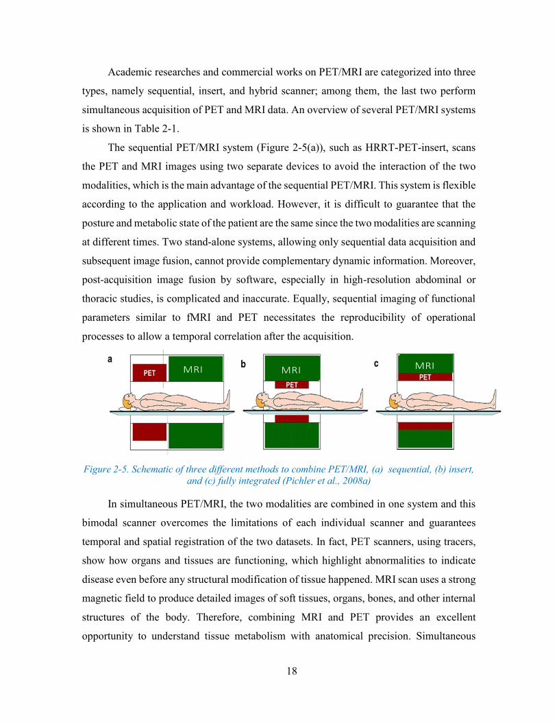
18
Academic researches and commercial works on PET/MRI are categorized into three
types, namely sequential, insert, and hybrid scanner; among them, the last two perform
simultaneous acquisition of PET and MRI data. An overview of several PET/MRI systems
is shown in Table 2-1.
The sequential PET/MRI system (Figure 2-5(a)), such as HRRT-PET-insert, scans
the PET and MRI images using two separate devices to avoid the interaction of the two
modalities, which is the main advantage of the sequential PET/MRI. This system is flexible
according to the application and workload. However, it is difficult to guarantee that the
posture and metabolic state of the patient are the same since the two modalities are scanning
at different times. Two stand-alone systems, allowing only sequential data acquisition and
subsequent image fusion, cannot provide complementary dynamic information. Moreover,
post-acquisition image fusion by software, especially in high-resolution abdominal or
thoracic studies, is complicated and inaccurate. Equally, sequential imaging of functional
parameters similar to fMRI and PET necessitates the reproducibility of operational
processes to allow a temporal correlation after the acquisition.
Figure 2-5. Schematic of three different methods to combine PET/MRI, (a) sequential, (b) insert,
and (c) fully integrated (Pichler et al., 2008a)
In simultaneous PET/MRI, the two modalities are combined in one system and this
bimodal scanner overcomes the limitations of each individual scanner and guarantees
temporal and spatial registration of the two datasets. In fact, PET scanners, using tracers,
show how organs and tissues are functioning, which highlight abnormalities to indicate
disease even before any structural modification of tissue happened. MRI scan uses a strong
magnetic field to produce detailed images of soft tissues, organs, bones, and other internal
structures of the body. Therefore, combining MRI and PET provides an excellent
opportunity to understand tissue metabolism with anatomical precision. Simultaneous
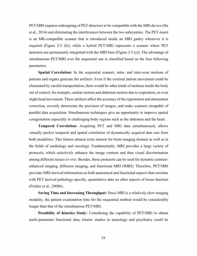
19
PET/MRI requires redesigning of PET detectors to be compatible with the MRI device (Hu
et al., 2014) and eliminating the interferences between the two subsystems. The PET-insert
is an MR-compatible scanner that is introduced inside an MRI gantry whenever it is
required (Figure 2-5 (b)), while a hybrid PET/MRI represents a scanner where PET
detectors are permanently integrated with the MRI bore (Figure 2-5 (c)). The advantage of
simultaneous PET/MRI over the sequential one is classified based on the four following
parameters.
Spatial Correlation: In the sequential scanner, intra- and inter-scan motions of
patients and organs generate the artifacts. Even if the external patient movement could be
eliminated by careful transportation, there would be other kinds of motions inside the body
out of control, for example, cardiac motion and abdomen motion due to respiration, or even
slight head movement. These artifacts affect the accuracy of the registration and attenuation
correction, severely deteriorate the precision of images, and make scanners incapable of
parallel data acquisition. Simultaneous techniques give an opportunity to improve spatial
coregistration especially in challenging body regions such as the abdomen and the heart.
Temporal Correlation: Acquiring PET and MRI data simultaneously allows
virtually perfect temporal and spatial correlation of dynamically acquired data sets from
both modalities. This feature attracts extra interest for brain imaging domain as well as in
the fields of cardiology and oncology. Fundamentally, MRI provides a large variety of
protocols, which selectively enhance the image contrast and thus visual discrimination
among different tissues in vivo. Besides, those protocols can be used for dynamic contrast-
enhanced imaging, diffusion imaging, and functional MRI (fMRI). Therefore, PET/MRI
provides MRI-derived information on both anatomical and functional aspects that correlate
with PET derived pathology-specific, quantitative data on other aspects of tissue function
(Pichler et al., 2008b).
Saving Time and Increasing Throughput: Since MRI is a relatively slow imaging
modality, the patient examination time for the sequential method would be considerably
longer than that of the simultaneous PET/MRI.
Possibility of Kinetics Study: Considering the capability of PET/MRI to obtain
multi-parameter functional data, kinetic studies in neurology and psychiatry could be
20
advanced by correlating the dynamic PET tracer or the drug distribution in various brain
structures with flow-dependent kinetics measured by the MRI.
Figure 2-6. Comparison of simultaneous PET/MRI, PET/CT, and sequential PET/MRI. (a) MRI,
(b) simultaneous PET/MRI, (c) CT, (d) PET/CT, (e) MRI, and (f) sequential PET/MRI (Richard et
al., 2016).
Figure 2-6 shows a comparison between simultaneous PET/MRI, PET/CT, and
sequential PET/MRI. Both sequential methods cause misregistration in the bladder region
while simultaneous PET/MRI makes a perfect alignment.
2.4. Interaction between PET and MRI
The inhomogeneity within the MRI bore is one of the significant problems to realize
a simultaneous PET/MRI. Additionally, the space inside the magnet constrains the PET
radial size. Moreover, magnetic interferences necessitate the use of photodetectors that are
insensitive to magnetic fields and require front-end electronics with non-magnetic material
and minimum heat radiation. The effect of APD-based PET modules on MRI mainly arises
from the PET electronics interactions with the RF and gradient coils. These interferences
must be minimized if high-frequency digital clocks are used for the PET front-end
electronics of PET and if eddy currents are produced in the electronic boards. To prevent
these interferences, commonly, a thin copper layer is employed to provide adequate
electromagnetic attenuation. However, this shielding results in a degradation of the MR
signal with about 30% reduction in the signal-to-noise ratio (SNR) (Pichler et al., 2006) .
misregisterbladder
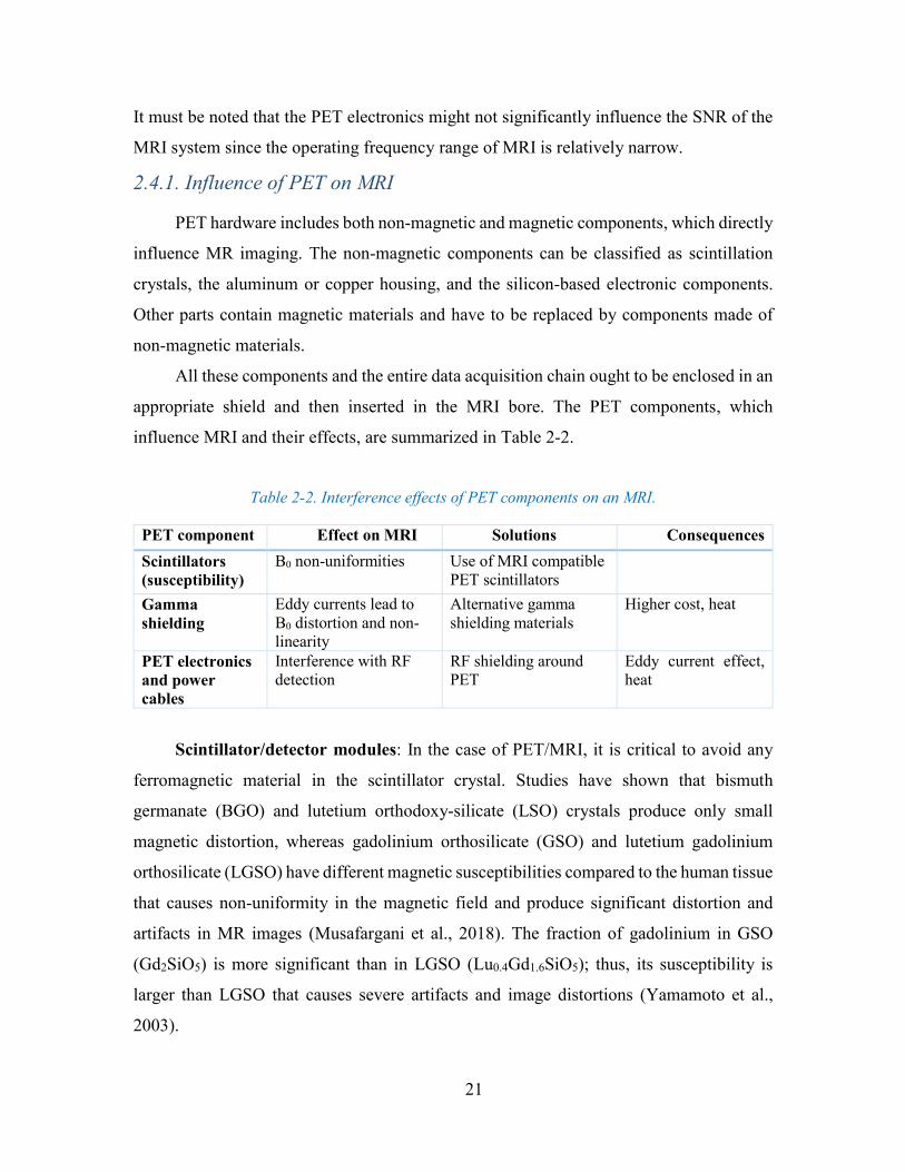
21
It must be noted that the PET electronics might not significantly influence the SNR of the
MRI system since the operating frequency range of MRI is relatively narrow.
2.4.1. Influence of PET on MRI
PET hardware includes both non-magnetic and magnetic components, which directly
influence MR imaging. The non-magnetic components can be classified as scintillation
crystals, the aluminum or copper housing, and the silicon-based electronic components.
Other parts contain magnetic materials and have to be replaced by components made of
non-magnetic materials.
All these components and the entire data acquisition chain ought to be enclosed in an
appropriate shield and then inserted in the MRI bore. The PET components, which
influence MRI and their effects, are summarized in Table 2-2.
Table 2-2. Interference effects of PET components on an MRI.
PET component Effect on MRI Solutions Consequences
Scintillators
(susceptibility)
B0 non-uniformities Use of MRI compatible
PET scintillators
Gamma
shielding
Eddy currents lead to
B0 distortion and non-
linearity
Alternative gamma
shielding materials
Higher cost, heat
PET electronics
and power
cables
Interference with RF
detection
RF shielding around
PET
Eddy current effect,
heat
Scintillator/detector modules: In the case of PET/MRI, it is critical to avoid any
ferromagnetic material in the scintillator crystal. Studies have shown that bismuth
germanate (BGO) and lutetium orthodoxy-silicate (LSO) crystals produce only small
magnetic distortion, whereas gadolinium orthosilicate (GSO) and lutetium gadolinium
orthosilicate (LGSO) have different magnetic susceptibilities compared to the human tissue
that causes non-uniformity in the magnetic field and produce significant distortion and
artifacts in MR images (Musafargani et al., 2018). The fraction of gadolinium in GSO
(Gd2SiO5) is more significant than in LGSO (Lu0.4Gd1.6SiO5); thus, its susceptibility is
larger than LGSO that causes severe artifacts and image distortions (Yamamoto et al.,
2003).
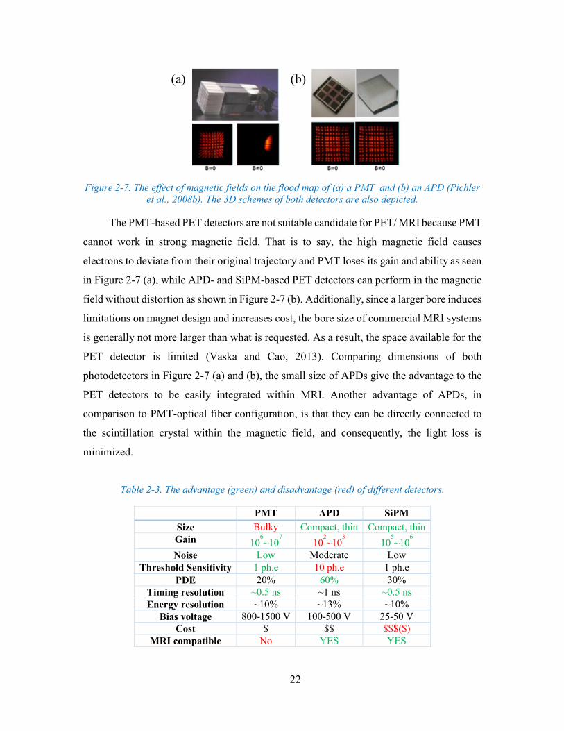
22
Figure 2-7. The effect of magnetic fields on the flood map of (a) a PMT and (b) an APD (Pichler
et al., 2008b). The 3D schemes of both detectors are also depicted.
The PMT-based PET detectors are not suitable candidate for PET/ MRI because PMT
cannot work in strong magnetic field. That is to say, the high magnetic field causes
electrons to deviate from their original trajectory and PMT loses its gain and ability as seen
in Figure 2-7 (a), while APD- and SiPM-based PET detectors can perform in the magnetic
field without distortion as shown in Figure 2-7 (b). Additionally, since a larger bore induces
limitations on magnet design and increases cost, the bore size of commercial MRI systems
is generally not more larger than what is requested. As a result, the space available for the
PET detector is limited (Vaska and Cao, 2013). Comparing dimensions of both
photodetectors in Figure 2-7 (a) and (b), the small size of APDs give the advantage to the
PET detectors to be easily integrated within MRI. Another advantage of APDs, in
comparison to PMT-optical fiber configuration, is that they can be directly connected to
the scintillation crystal within the magnetic field, and consequently, the light loss is
minimized.
Table 2-3. The advantage (green) and disadvantage (red) of different detectors.
PMT APD SiPM
Size Bulky Compact, thin Compact, thin
Gain 106
~107
102
~103
105
~106
Noise Low Moderate Low
Threshold Sensitivity 1 ph.e 10 ph.e 1 ph.e
PDE 20% 60% 30%
Timing resolution ~0.5 ns ~1 ns ~0.5 ns
Energy resolution ~10% ~13% ~10%
Bias voltage 800-1500 V 100-500 V 25-50 V
Cost $ $$ $$$($)
MRI compatible No YES YES
(a) (b)
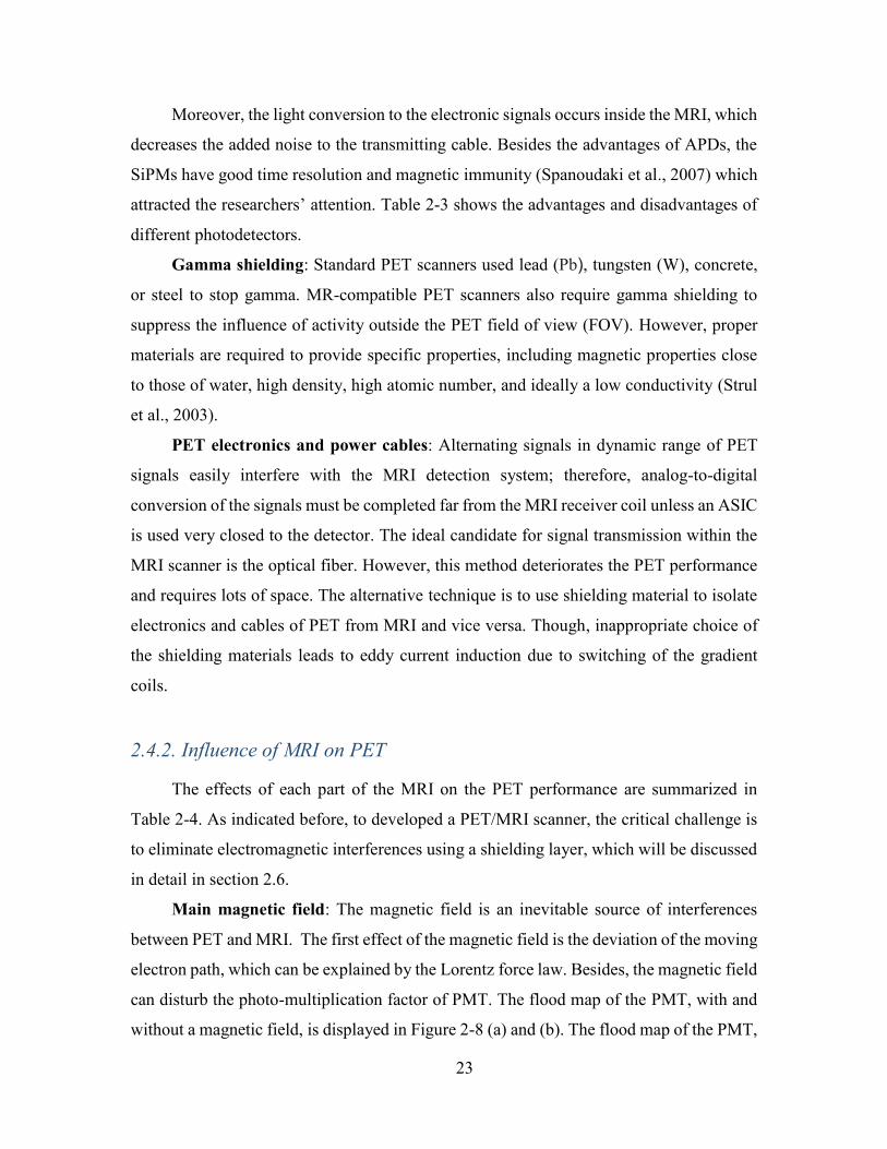
23
Moreover, the light conversion to the electronic signals occurs inside the MRI, which
decreases the added noise to the transmitting cable. Besides the advantages of APDs, the
SiPMs have good time resolution and magnetic immunity (Spanoudaki et al., 2007) which
attracted the researchers’ attention. Table 2-3 shows the advantages and disadvantages of
different photodetectors.
Gamma shielding: Standard PET scanners used lead (Pb), tungsten (W), concrete,
or steel to stop gamma. MR-compatible PET scanners also require gamma shielding to
suppress the influence of activity outside the PET field of view (FOV). However, proper
materials are required to provide specific properties, including magnetic properties close
to those of water, high density, high atomic number, and ideally a low conductivity (Strul
et al., 2003).
PET electronics and power cables: Alternating signals in dynamic range of PET
signals easily interfere with the MRI detection system; therefore, analog-to-digital
conversion of the signals must be completed far from the MRI receiver coil unless an ASIC
is used very closed to the detector. The ideal candidate for signal transmission within the
MRI scanner is the optical fiber. However, this method deteriorates the PET performance
and requires lots of space. The alternative technique is to use shielding material to isolate
electronics and cables of PET from MRI and vice versa. Though, inappropriate choice of
the shielding materials leads to eddy current induction due to switching of the gradient
coils.
2.4.2. Influence of MRI on PET
The effects of each part of the MRI on the PET performance are summarized in
Table 2-4. As indicated before, to developed a PET/MRI scanner, the critical challenge is
to eliminate electromagnetic interferences using a shielding layer, which will be discussed
in detail in section 2.6.
Main magnetic field: The magnetic field is an inevitable source of interferences
between PET and MRI. The first effect of the magnetic field is the deviation of the moving
electron path, which can be explained by the Lorentz force law. Besides, the magnetic field
can disturb the photo-multiplication factor of PMT. The flood map of the PMT, with and
without a magnetic field, is displayed in Figure 2-8 (a) and (b). The flood map of the PMT,
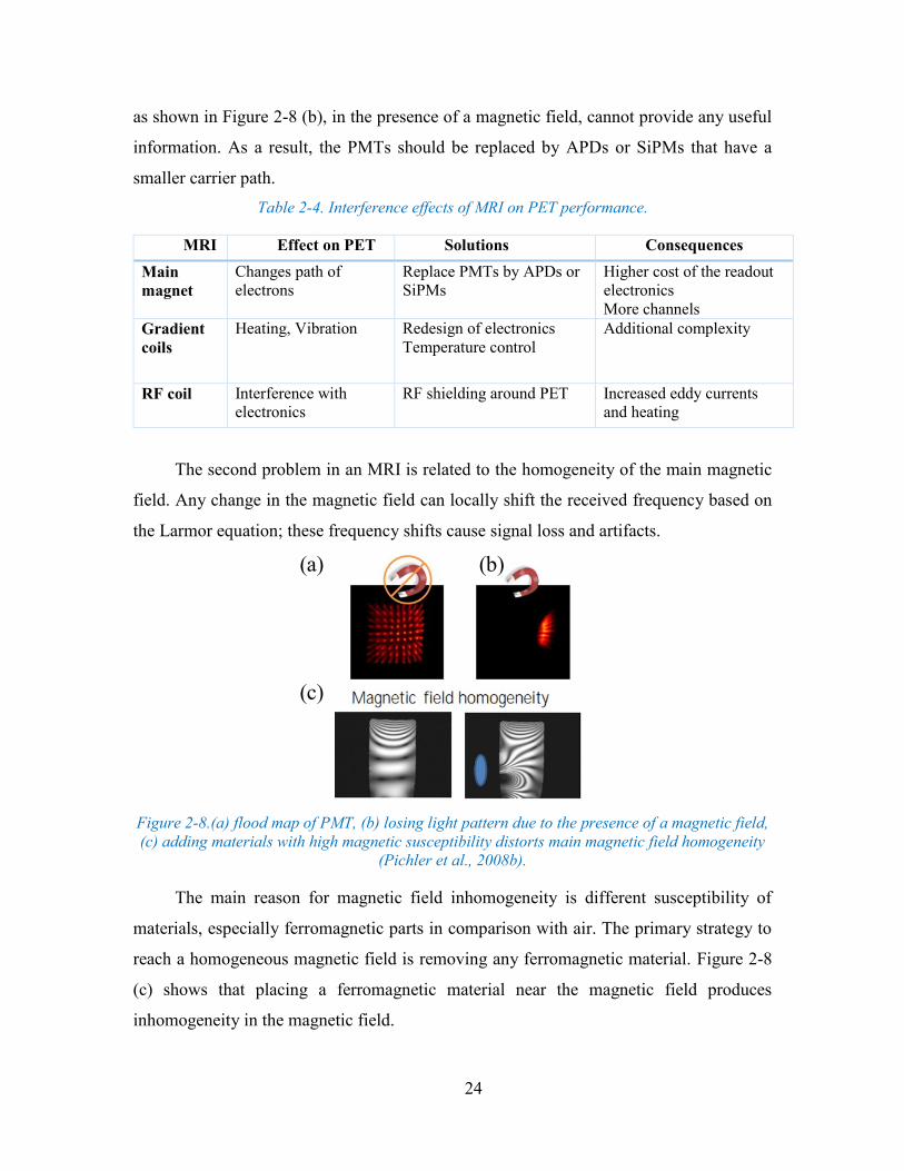
24
as shown in Figure 2-8 (b), in the presence of a magnetic field, cannot provide any useful
information. As a result, the PMTs should be replaced by APDs or SiPMs that have a
smaller carrier path.
Table 2-4. Interference effects of MRI on PET performance.
MRI Effect on PET Solutions Consequences
Main
magnet
Changes path of
electrons
Replace PMTs by APDs or
SiPMs
Higher cost of the readout
electronics
More channels
Gradient
coils
Heating, Vibration Redesign of electronics
Temperature control
Additional complexity
RF coil Interference with
electronics
RF shielding around PET Increased eddy currents
and heating
The second problem in an MRI is related to the homogeneity of the main magnetic
field. Any change in the magnetic field can locally shift the received frequency based on
the Larmor equation; these frequency shifts cause signal loss and artifacts.
Figure 2-8.(a) flood map of PMT, (b) losing light pattern due to the presence of a magnetic field,
(c) adding materials with high magnetic susceptibility distorts main magnetic field homogeneity
(Pichler et al., 2008b).
The main reason for magnetic field inhomogeneity is different susceptibility of
materials, especially ferromagnetic parts in comparison with air. The primary strategy to
reach a homogeneous magnetic field is removing any ferromagnetic material. Figure 2-8
(c) shows that placing a ferromagnetic material near the magnetic field produces
inhomogeneity in the magnetic field.
(a) (b)
(c)
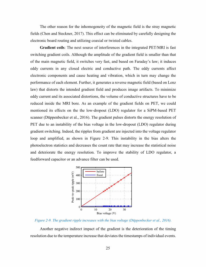
25
The other reason for the inhomogeneity of the magnetic field is the stray magnetic
fields (Chen and Steckner, 2017). This effect can be eliminated by carefully designing the
electronic board routing and utilizing coaxial or twisted cables.
Gradient coils: The next source of interferences in the integrated PET/MRI is fast
switching gradient coils. Although the amplitude of the gradient field is smaller than that
of the main magnetic field, it switches very fast, and based on Faraday’s law; it induces
eddy currents in any closed electric and conductive path. The eddy currents affect
electronic components and cause heating and vibration, which in turn may change the
performance of each element. Further, it generates a reverse magnetic field (based on Lenz
law) that distorts the intended gradient field and produces image artifacts. To minimize
eddy current and its associated distortions, the volume of conductive structures have to be
reduced inside the MRI bore. As an example of the gradient fields on PET, we could
mentioned its effects on the the low-dropout (LDO) regulator for a SiPM-based PET
scanner (Düppenbecker et al., 2016). The gradient pulses distorts the energy resolution of
PET due to an instability of the bias voltage in the low-dropout (LDO) regulator during
gradient switching. Indeed, the ripples from gradient are injected into the voltage regulator
loop and amplified, as shown in Figure 2-9. This instability in the bias alters the
photoelectron statistics and decreases the count rate that may increase the statistical noise
and deteriorate the energy resolution. To improve the stability of LDO regulator, a
feedforward capacitor or an advance filter can be used.
Figure 2-9. The gradient ripple increases with the bias voltage (Düppenbecker et al., 2016).
Another negative indirect impact of the gradient is the deterioration of the timing
resolution due to the temperature increase that deviates the timestamps of individual events.
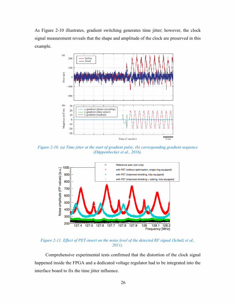
26
As Figure 2-10 illustrates, gradient switching generates time jitter; however, the clock
signal measurement reveals that the shape and amplitude of the clock are preserved in this
example.
Figure 2-10. (a) Time jitter at the start of gradient pulse, (b) corresponding gradient sequence
(Düppenbecker et al., 2016).
Figure 2-11. Effect of PET-insert on the noise level of the detected RF signal (Schulz et al.,
2011).
Comprehensive experimental tests confirmed that the distortion of the clock signal
happened inside the FPGA and a dedicated voltage regulator had to be integrated into the
interface board to fix the time jitter influence.
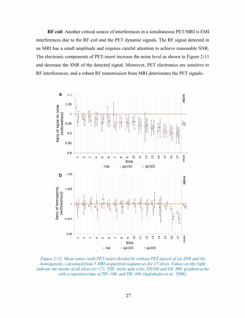
27
RF coil: Another critical source of interferences in a simultaneous PET/MRI is EMI
interferences due to the RF coil and the PET dynamic signals. The RF signal detected in
an MRI has a small amplitude and requires careful attention to achieve reasonable SNR.
The electronic components of PET-insert increase the noise level as shown in Figure 2-11
and decrease the SNR of the detected signal. Moreover, PET electronics are sensitive to
RF interferences, and a robust RF transmission from MRI deteriorates the PET signals.
Figure 2-12. Mean ratios (with PET-insert divided by without PET-insert) of (a) SNR and (b)
homogeneity, calculated from 5 MRI acquisition sequencses for 17 slices. Values on the right
indicate the means of all slices (n=17); TSE: turbo spin echo, GE100 and GE 300: gradient-echo
with a repetition time of TR=100, and TR=300 (Judenhofer et al., 2008).
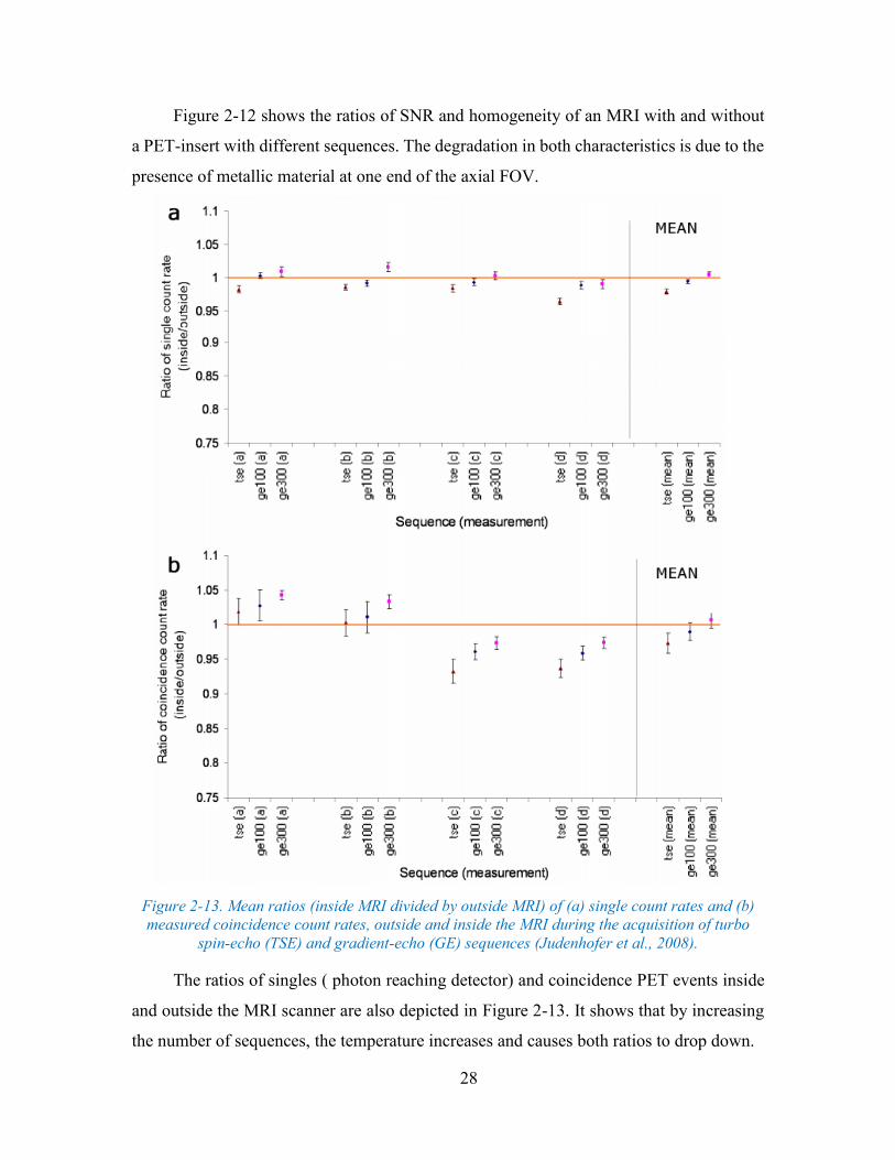
28
Figure 2-12 shows the ratios of SNR and homogeneity of an MRI with and without
a PET-insert with different sequences. The degradation in both characteristics is due to the
presence of metallic material at one end of the axial FOV.
Figure 2-13. Mean ratios (inside MRI divided by outside MRI) of (a) single count rates and (b)
measured coincidence count rates, outside and inside the MRI during the acquisition of turbo
spin-echo (TSE) and gradient-echo (GE) sequences (Judenhofer et al., 2008).
The ratios of singles ( photon reaching detector) and coincidence PET events inside
and outside the MRI scanner are also depicted in Figure 2-13. It shows that by increasing
the number of sequences, the temperature increases and causes both ratios to drop down.
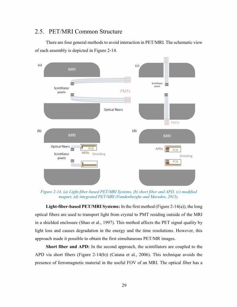
29
2.5. PET/MRI Common Structure
There are four general methods to avoid interaction in PET/MRI. The schematic view
of each assembly is depicted in Figure 2-14.
Figure 2-14. (a) Light-fiber-based PET/MRI Systems, (b) short fiber and APD, (c) modified
magnet, (d) integrated PET/MRI (Vandenberghe and Marsden, 2015).
Light-fiber-based PET/MRI Systems: In the first method (Figure 2-14(a)), the long
optical fibers are used to transport light from crystal to PMT residing outside of the MRI
in a shielded enclosure (Shao et al., 1997). This method affects the PET signal quality by
light loss and causes degradation in the energy and the time resolutions. However, this
approach made it possible to obtain the first simultaneous PET/MR images.
Short fiber and APD: In the second approach, the scintillators are coupled to the
APD via short fibers (Figure 2-14(b)) (Catana et al., 2006). This technique avoids the
presence of ferromagnetic material in the useful FOV of an MRI. The optical fiber has a
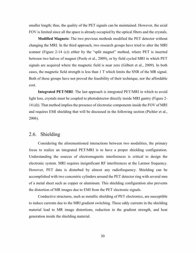
30
smaller length; thus, the quality of the PET signals can be maintained. However, the axial
FOV is limited since all the space is already occupied by the optical fibers and the crystals.
Modified Magnets: The two previous methods modified the PET detector without
changing the MRI. In the third approach, two research groups have tried to alter the MRI
scanner (Figure 2-14 (c)) either by the “split magnet” method, where PET is inserted
between two halves of magnet (Poole et al., 2009), or by field cycled MRI in which PET
signals are acquired where the magnetic field is near zero (Gilbert et al., 2009). In both
cases, the magnetic field strength is less than 1 T which limits the SNR of the MR signal.
Both of these groups have not proved the feasibility of their technique, nor the affordable
cost.
Integrated PET/MRI: The last approach is integrated PET/MRI in which to avoid
light loss, crystals must be coupled to photodetector directly inside MRI gantry (Figure 2-
14 (d)). That method implies the presence of electronic components inside the FOV of MRI
and requires EMI shielding that will be discussed in the following section (Pichler et al.,
2006).
2.6. Shielding
Considering the aforementioned interactions between two modalities, the primary
focus to realize an integrated PET/MRI is to have a proper shielding configuration.
Understanding the sources of electromagnetic interferences is critical to design the
electronic system. MRI requires insignificant RF interferences at the Larmor frequency.
However, PET data is disturbed by almost any radiofrequency. Shielding can be
accomplished with two concentric cylinders around the PET detector ring with several mm
of a metal sheet such as copper or aluminum. This shielding configuration also prevents
the distortion of MR images due to EMI from the PET electronic signals.
Conductive structures, such as metallic shielding of PET electronics, are susceptible
to induce currents due to the MRI gradient switching. These eddy currents in the shielding
material lead to MR image distortions, reduction in the gradient strength, and heat
generation inside the shielding material.
31
2.6.1. Shielding Effectiveness
The efficiency of a material to reduce the electromagnetic signal is defined by a
parameter called shielding effectiveness (SE). For a plate of conductive material, the SE is
defined as (Kang et al., 2009)
/2/0 log20log20log20)( tt
s
plate eedBSE , (2.2)
where t is the thickness of the material used for the shielding, 0 is the intrinsic impedance
of free space which is equal to 377 Ω, s is the intrinsic impedance of the shielding material
defined as /2 fs , and f/1 is the skin depth of the material (usually a few
mm). The σ is the electrical conductivity of the material [S/m], f represents the frequency,
and µ is the magnetic permeability of material.
Another method to shield the electromagnetic field is using a mesh of the shielding
material. Mesh shielding is expected to improve the MR image quality because of the
reduction in the area of the conductive material in the MRI bore. However, the shielding
effectiveness degrades due to the presence of holes. For a mesh design with multiple
circular apertures, the SE is described as (Kang et al., 2009)
d
tn
ddBSEmesh 32log10
2log20)(
, (2.3)
where the λ is the wavelength of the electromagnetic source, d is the diameter of a circular
hole, n is the number of aperture in a distance of λ/2 and t is the thickness of the mesh layer.
Figure 2-15 (a) and (b) show a comparison between SE of copper plate and mesh shielding.
As the curves display, the required thickness for a copper mesh configuration is almost one
order of magnitude higher than that of a copper plate.
In clinical scanners, a magnetic field of 3 T is commonly used. This magnetic field
generates a Larmor frequency of 127.7 MHz. To use a copper plate to shield this
electromagnetic source, and assuming the criterion of 5 skin depths based on Equation
(2.2), a thickness of about 30 µm of copper is sufficient. This copper plate shields the
electromagnetic field by SE of 130 dB. However, due to the conductivity of copper, the
gradient induces eddy currents leading to a rise in the temperature of the layer.
Consequently, using plate shielding is not a satisfactory technique in the presence of a
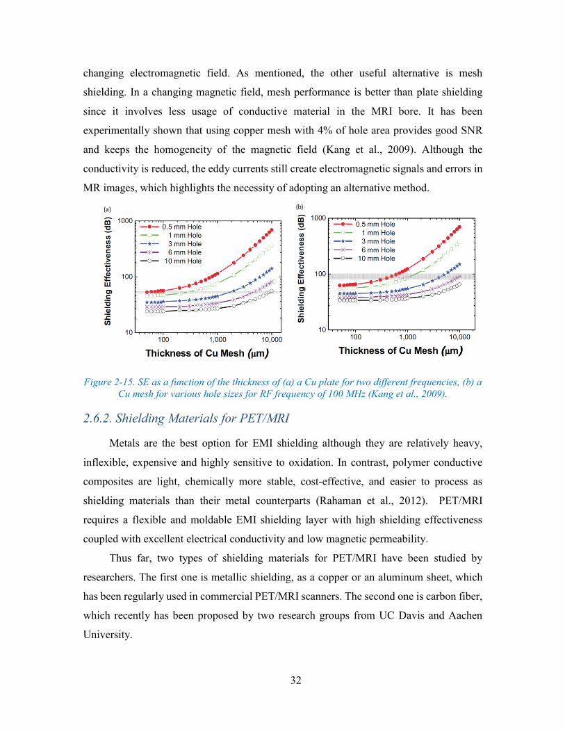
32
changing electromagnetic field. As mentioned, the other useful alternative is mesh
shielding. In a changing magnetic field, mesh performance is better than plate shielding
since it involves less usage of conductive material in the MRI bore. It has been
experimentally shown that using copper mesh with 4% of hole area provides good SNR
and keeps the homogeneity of the magnetic field (Kang et al., 2009). Although the
conductivity is reduced, the eddy currents still create electromagnetic signals and errors in
MR images, which highlights the necessity of adopting an alternative method.
Figure 2-15. SE as a function of the thickness of (a) a Cu plate for two different frequencies, (b) a
Cu mesh for various hole sizes for RF frequency of 100 MHz (Kang et al., 2009).
2.6.2. Shielding Materials for PET/MRI
Metals are the best option for EMI shielding although they are relatively heavy,
inflexible, expensive and highly sensitive to oxidation. In contrast, polymer conductive
composites are light, chemically more stable, cost-effective, and easier to process as
shielding materials than their metal counterparts (Rahaman et al., 2012). PET/MRI
requires a flexible and moldable EMI shielding layer with high shielding effectiveness
coupled with excellent electrical conductivity and low magnetic permeability.
Thus far, two types of shielding materials for PET/MRI have been studied by
researchers. The first one is metallic shielding, as a copper or an aluminum sheet, which
has been regularly used in commercial PET/MRI scanners. The second one is carbon fiber,
which recently has been proposed by two research groups from UC Davis and Aachen
University.
(a) (b)
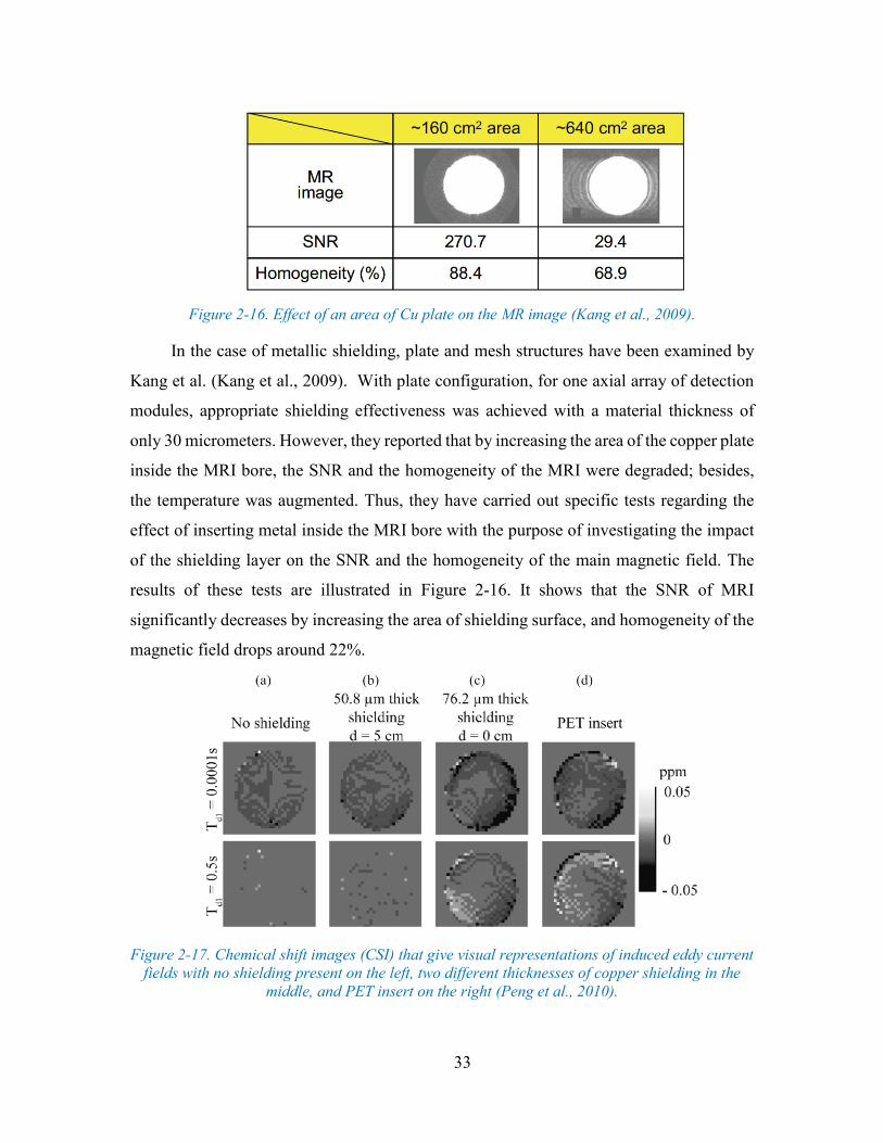
33
Figure 2-16. Effect of an area of Cu plate on the MR image (Kang et al., 2009).
In the case of metallic shielding, plate and mesh structures have been examined by
Kang et al. (Kang et al., 2009). With plate configuration, for one axial array of detection
modules, appropriate shielding effectiveness was achieved with a material thickness of
only 30 micrometers. However, they reported that by increasing the area of the copper plate
inside the MRI bore, the SNR and the homogeneity of the MRI were degraded; besides,
the temperature was augmented. Thus, they have carried out specific tests regarding the
effect of inserting metal inside the MRI bore with the purpose of investigating the impact
of the shielding layer on the SNR and the homogeneity of the main magnetic field. The
results of these tests are illustrated in Figure 2-16. It shows that the SNR of MRI
significantly decreases by increasing the area of shielding surface, and homogeneity of the
magnetic field drops around 22%.
Figure 2-17. Chemical shift images (CSI) that give visual representations of induced eddy current
fields with no shielding present on the left, two different thicknesses of copper shielding in the
middle, and PET insert on the right (Peng et al., 2010).
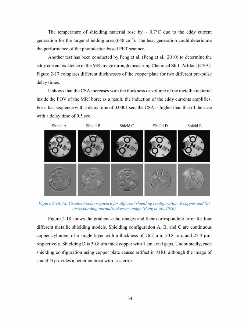
34
The temperature of shielding material rose by ~ 0.7°C due to the eddy current
generation for the larger shielding area (640 cm2). The heat generation could deteriorate
the performance of the photodector-based PET scanner.
Another test has been conducted by Peng et al. (Peng et al., 2010) to determine the
eddy current existence in the MR image through measuring Chemical Shift Artifact (CSA).
Figure 2-17 compares different thicknesses of the copper plate for two different pre-pulse
delay times.
It shows that the CSA increases with the thickness or volume of the metallic material
inside the FOV of the MRI bore; as a result, the induction of the eddy currents amplifies.
For a fast sequence with a delay time of 0.0001 sec, the CSA is higher than that of the case
with a delay time of 0.5 sec.
Figure 2-18. (a) Gradient-echo sequence for different shielding configuration of copper and (b)
corresponding normalized error image (Peng et al., 2010).
Figure 2-18 shows the gradient-echo images and their corresponding error for four
different metallic shielding models. Shielding configuration A, B, and C are continuous
copper cylinders of a single layer with a thickness of 76.2 µm, 50.8 µm, and 25.4 µm,
respectively. Shielding D is 50.8 µm thick copper with 1 cm axial gaps. Undoubtedly, each
shielding configuration using copper plate causes artifact in MRI, although the image of
shield D provides a better contrast with less error.
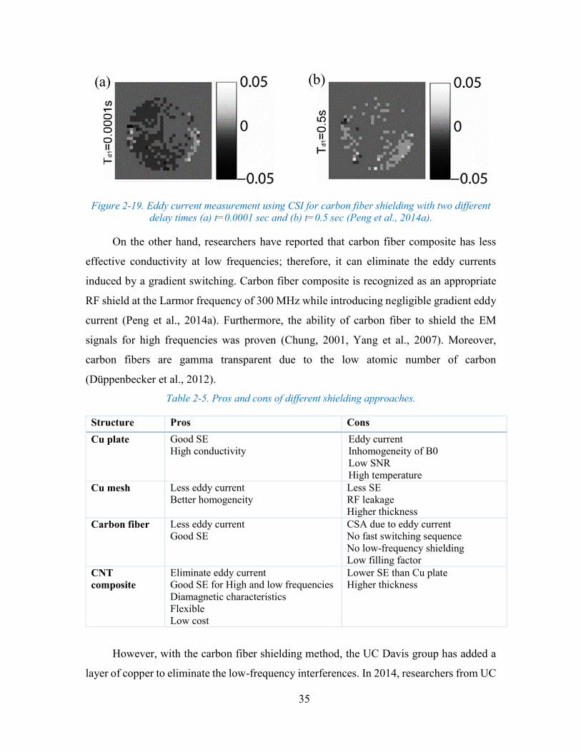
35
Figure 2-19. Eddy current measurement using CSI for carbon fiber shielding with two different
delay times (a) t=0.0001 sec and (b) t=0.5 sec (Peng et al., 2014a).
On the other hand, researchers have reported that carbon fiber composite has less
effective conductivity at low frequencies; therefore, it can eliminate the eddy currents
induced by a gradient switching. Carbon fiber composite is recognized as an appropriate
RF shield at the Larmor frequency of 300 MHz while introducing negligible gradient eddy
current (Peng et al., 2014a). Furthermore, the ability of carbon fiber to shield the EM
signals for high frequencies was proven (Chung, 2001, Yang et al., 2007). Moreover,
carbon fibers are gamma transparent due to the low atomic number of carbon
(Düppenbecker et al., 2012).
Table 2-5. Pros and cons of different shielding approaches.
Structure Pros Cons
Cu plate Good SE
High conductivity
Eddy current
Inhomogeneity of B0
Low SNR
High temperature
Cu mesh Less eddy current
Better homogeneity
Less SE
RF leakage
Higher thickness
Carbon fiber Less eddy current
Good SE
CSA due to eddy current
No fast switching sequence
No low-frequency shielding
Low filling factor
CNT
composite
Eliminate eddy current
Good SE for High and low frequencies
Diamagnetic characteristics
Flexible
Low cost
Lower SE than Cu plate
Higher thickness
However, with the carbon fiber shielding method, the UC Davis group has added a
layer of copper to eliminate the low-frequency interferences. In 2014, researchers from UC
(a) (b)
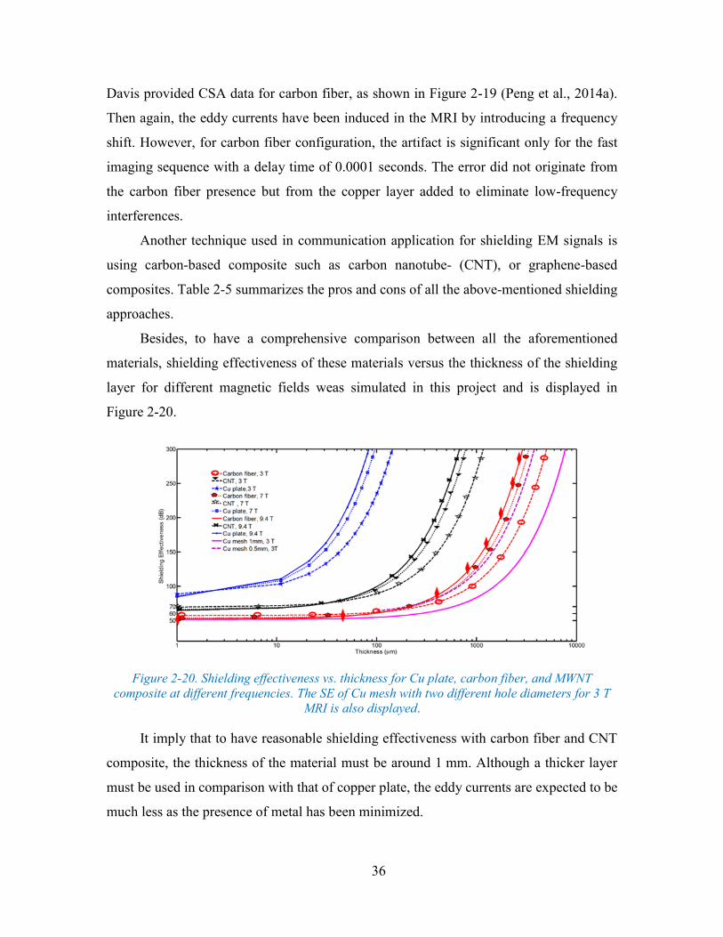
36
Davis provided CSA data for carbon fiber, as shown in Figure 2-19 (Peng et al., 2014a).
Then again, the eddy currents have been induced in the MRI by introducing a frequency
shift. However, for carbon fiber configuration, the artifact is significant only for the fast
imaging sequence with a delay time of 0.0001 seconds. The error did not originate from
the carbon fiber presence but from the copper layer added to eliminate low-frequency
interferences.
Another technique used in communication application for shielding EM signals is
using carbon-based composite such as carbon nanotube- (CNT), or graphene-based
composites. Table 2-5 summarizes the pros and cons of all the above-mentioned shielding
approaches.
Besides, to have a comprehensive comparison between all the aforementioned
materials, shielding effectiveness of these materials versus the thickness of the shielding
layer for different magnetic fields weas simulated in this project and is displayed in
Figure 2-20.
Figure 2-20. Shielding effectiveness vs. thickness for Cu plate, carbon fiber, and MWNT
composite at different frequencies. The SE of Cu mesh with two different hole diameters for 3 T
MRI is also displayed.
It imply that to have reasonable shielding effectiveness with carbon fiber and CNT
composite, the thickness of the material must be around 1 mm. Although a thicker layer
must be used in comparison with that of copper plate, the eddy currents are expected to be
much less as the presence of metal has been minimized.
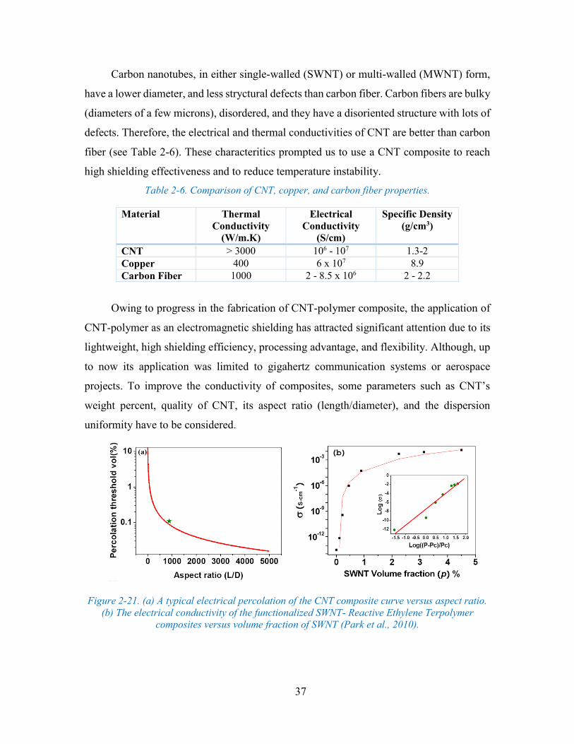
37
Carbon nanotubes, in either single-walled (SWNT) or multi-walled (MWNT) form,
have a lower diameter, and less stryctural defects than carbon fiber. Carbon fibers are bulky
(diameters of a few microns), disordered, and they have a disoriented structure with lots of
defects. Therefore, the electrical and thermal conductivities of CNT are better than carbon
fiber (see Table 2-6). These characteritics prompted us to use a CNT composite to reach
high shielding effectiveness and to reduce temperature instability.
Table 2-6. Comparison of CNT, copper, and carbon fiber properties.
Material Thermal
Conductivity
(W/m.K)
Electrical
Conductivity
(S/cm)
Specific Density
(g/cm3)
CNT > 3000 106 - 107 1.3-2
Copper 400 6 x 10⁷ 8.9
Carbon Fiber 1000 2 - 8.5 x 10⁶ 2 - 2.2
Owing to progress in the fabrication of CNT-polymer composite, the application of
CNT-polymer as an electromagnetic shielding has attracted significant attention due to its
lightweight, high shielding efficiency, processing advantage, and flexibility. Although, up
to now its application was limited to gigahertz communication systems or aerospace
projects. To improve the conductivity of composites, some parameters such as CNT’s
weight percent, quality of CNT, its aspect ratio (length/diameter), and the dispersion
uniformity have to be considered.
Figure 2-21. (a) A typical electrical percolation of the CNT composite curve versus aspect ratio.
(b) The electrical conductivity of the functionalized SWNT- Reactive Ethylene Terpolymer
composites versus volume fraction of SWNT (Park et al., 2010).
(b)
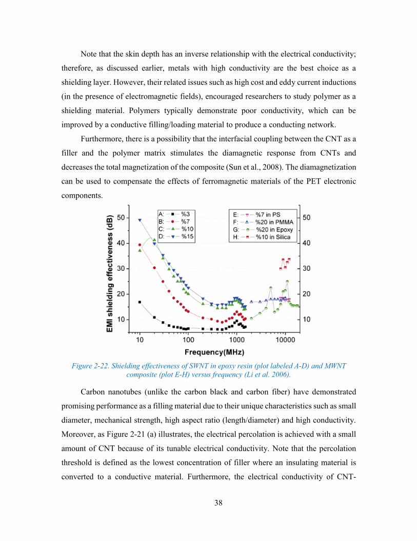
38
Note that the skin depth has an inverse relationship with the electrical conductivity;
therefore, as discussed earlier, metals with high conductivity are the best choice as a
shielding layer. However, their related issues such as high cost and eddy current inductions
(in the presence of electromagnetic fields), encouraged researchers to study polymer as a
shielding material. Polymers typically demonstrate poor conductivity, which can be
improved by a conductive filling/loading material to produce a conducting network.
Furthermore, there is a possibility that the interfacial coupling between the CNT as a
filler and the polymer matrix stimulates the diamagnetic response from CNTs and
decreases the total magnetization of the composite (Sun et al., 2008). The diamagnetization
can be used to compensate the effects of ferromagnetic materials of the PET electronic
components.
Figure 2-22. Shielding effectiveness of SWNT in epoxy resin (plot labeled A-D) and MWNT
composite (plot E-H) versus frequency (Li et al. 2006).
Carbon nanotubes (unlike the carbon black and carbon fiber) have demonstrated
promising performance as a filling material due to their unique characteristics such as small
diameter, mechanical strength, high aspect ratio (length/diameter) and high conductivity.
Moreover, as Figure 2-21 (a) illustrates, the electrical percolation is achieved with a small
amount of CNT because of its tunable electrical conductivity. Note that the percolation
threshold is defined as the lowest concentration of filler where an insulating material is
converted to a conductive material. Furthermore, the electrical conductivity of CNT-
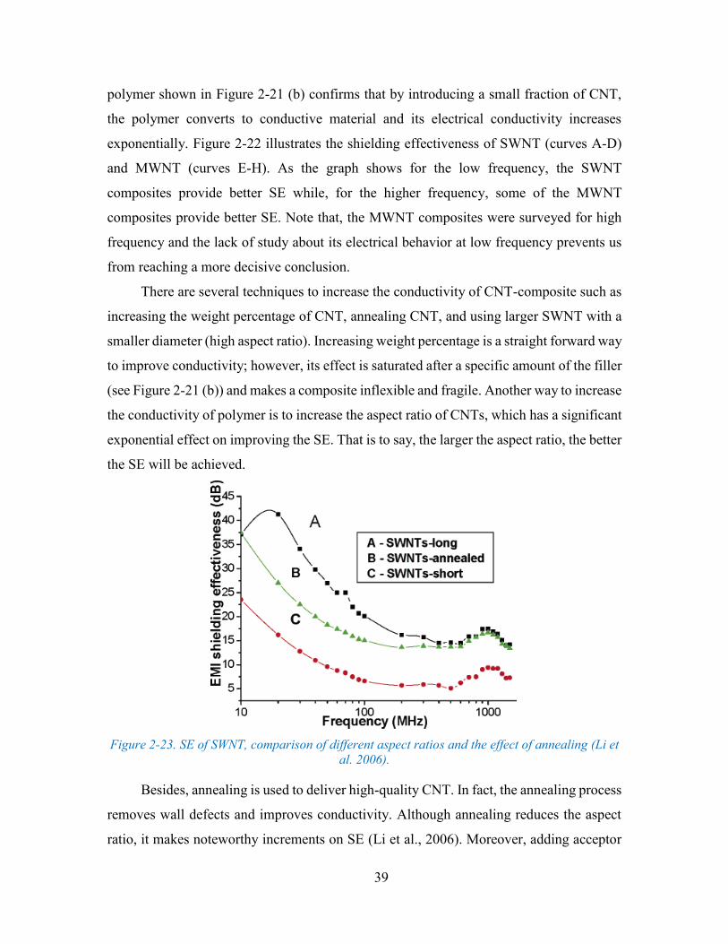
39
polymer shown in Figure 2-21 (b) confirms that by introducing a small fraction of CNT,
the polymer converts to conductive material and its electrical conductivity increases
exponentially. Figure 2-22 illustrates the shielding effectiveness of SWNT (curves A-D)
and MWNT (curves E-H). As the graph shows for the low frequency, the SWNT
composites provide better SE while, for the higher frequency, some of the MWNT
composites provide better SE. Note that, the MWNT composites were surveyed for high
frequency and the lack of study about its electrical behavior at low frequency prevents us
from reaching a more decisive conclusion.
There are several techniques to increase the conductivity of CNT-composite such as
increasing the weight percentage of CNT, annealing CNT, and using larger SWNT with a
smaller diameter (high aspect ratio). Increasing weight percentage is a straight forward way
to improve conductivity; however, its effect is saturated after a specific amount of the filler
(see Figure 2-21 (b)) and makes a composite inflexible and fragile. Another way to increase
the conductivity of polymer is to increase the aspect ratio of CNTs, which has a significant
exponential effect on improving the SE. That is to say, the larger the aspect ratio, the better
the SE will be achieved.
Figure 2-23. SE of SWNT, comparison of different aspect ratios and the effect of annealing (Li et
al. 2006).
Besides, annealing is used to deliver high-quality CNT. In fact, the annealing process
removes wall defects and improves conductivity. Although annealing reduces the aspect
ratio, it makes noteworthy increments on SE (Li et al., 2006). Moreover, adding acceptor
40
material, such as phosphor, increases the conductivity of CNT (Ishii, 2007). However, the
P-doped CNTs are not stable. The SE of an SWNT with two different aspect ratios and the
SE of the short one, while it is annealed, have been displayed in Figure 2-23. As the figure
confirms, the long SWNT provides a higher amount of SE and annealing the short one
improves the SE in a way that, at the higher frequencies, it reaches to the SE level of long
SWNT.
The maximum shielding effectiveness of CNT-composite, reported in the literature,
is 47 dB at 10 MHz (Li et al., 2006). This shielding property of CNT composite is used in
space applications due to its lightweight. For PET/MRI application, we require at least
60 dB of shielding effectiveness to eliminate MRI interferences efficiently on the PET data
and vice versa. In fact, the signals passing through the shielding layer must be decreased
by 6-order of magnitude.
Furthermore, a multi-shell configuration of any material results in a considerable
improvement in the shielding effectiveness (Truhn et al., 2011) and can be easily
incorporated into existing designs by coating both the inner and outer surface of the PET
enclosure. These arrangements are expected to reduce the potential image artifacts
associated with induced eddy currents in the shielding enclosures.
2.7. Eddy Currents
Eddy currents are related to the fast and robustly switching magnetic gradient fields.
When gradient fields are switching, according to Faraday’s induction law, eddy currents
are induced into neighboring electrically-conductive structures. The gradient slew rate of
MRI systems is a few hundred T/m/s. For instance, a gradient with a slew rate (dB/dt)
equals to 100 T/m/s induces the voltage (Faraday’s law) of 10 mV per cm2,
mVAdtdBdtdV 10)01.001.0(100// , which causes a 10 A current in a
loop with a resistance of 1 mΩ (Düppenbecker et al., 2012). The eddy currents produce a
reverse magnetic field which is added to the gradient field. According to the amplitude of
the opposite magnetic field, it can cause image distortions and vibrations, especially in
gradient-echo-based MRI sequences. Furthermore, the induced eddy currents cause local
heating and interferences with the electronics.
41
As the eddy currents circulate in a plane, they produce heat. That is usually an
undesirable consequence and is referred to as the eddy current loss. By assuming certain
conditions, namely uniform material, constant magnetic field, zero skin effect, etc..., the
power loss, because of eddy currents per unit mass for a thin sheet, is calculated from the
following equation:
D
fdBP
6
2222
(2.4)
where P is the power loss per unit mass (W/kg), B is the peak magnetic field (T), d is the
sheet thickness, f is the frequency (Hz), ρ is the resistivity of the material (Ω m), and D is
the density of the material (kg/m3).
The penetration depth of eddy current (skin depth) for a conductor can be calculated
as:
f/1 (2.5)
where f is the frequency (Hz), μ is the magnetic permeability of the material (H/m), and σ
is the electrical conductivity of the material (S/m).
2.8. Conventional Method to Measure the SE
To measure the electromagnetic shielding effectiveness of a conductive film, the
ASTM D4935-99 standard is a common method (ASTM, 1999). The SE measurement is
normally performed with a Network Analyzer using the S11 parameter. Figure 2-24 (a)
and (b) display the ASTM D4935-99 setup and its required specimens, respectively.
However, the ASTM D4935-99 standard has some restrictions that lead to the
generation of different results in different labs. These limitations are classified as variations
in the tester fabrication, unclear explanation of some details, surface finishing and
dimensions at the ends of the tester where connectors are attached. In addition, with this
standard, the SE tester requires a disk with a diameter of 133 mm, which appears to be a
small sample size in comparison to other SE testing methods. However, in the case of
nanotechnology systems such as nanowires and nanocomposite, the cost of fabricating that
size of specimens for initial characterization seems irrational. Besides, the ASTM D4935-
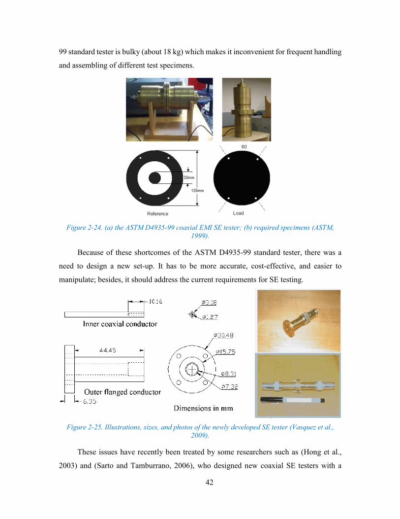
42
99 standard tester is bulky (about 18 kg) which makes it inconvenient for frequent handling
and assembling of different test specimens.
Figure 2-24. (a) the ASTM D4935-99 coaxial EMI SE tester; (b) required specimens (ASTM,
1999).
Because of these shortcomes of the ASTM D4935-99 standard tester, there was a
need to design a new set-up. It has to be more accurate, cost-effective, and easier to
manipulate; besides, it should address the current requirements for SE testing.
Figure 2-25. Illustrations, sizes, and photos of the newly developed SE tester (Vasquez et al.,
2009).
These issues have recently been treated by some researchers such as (Hong et al.,
2003) and (Sarto and Tamburrano, 2006), who designed new coaxial SE testers with a
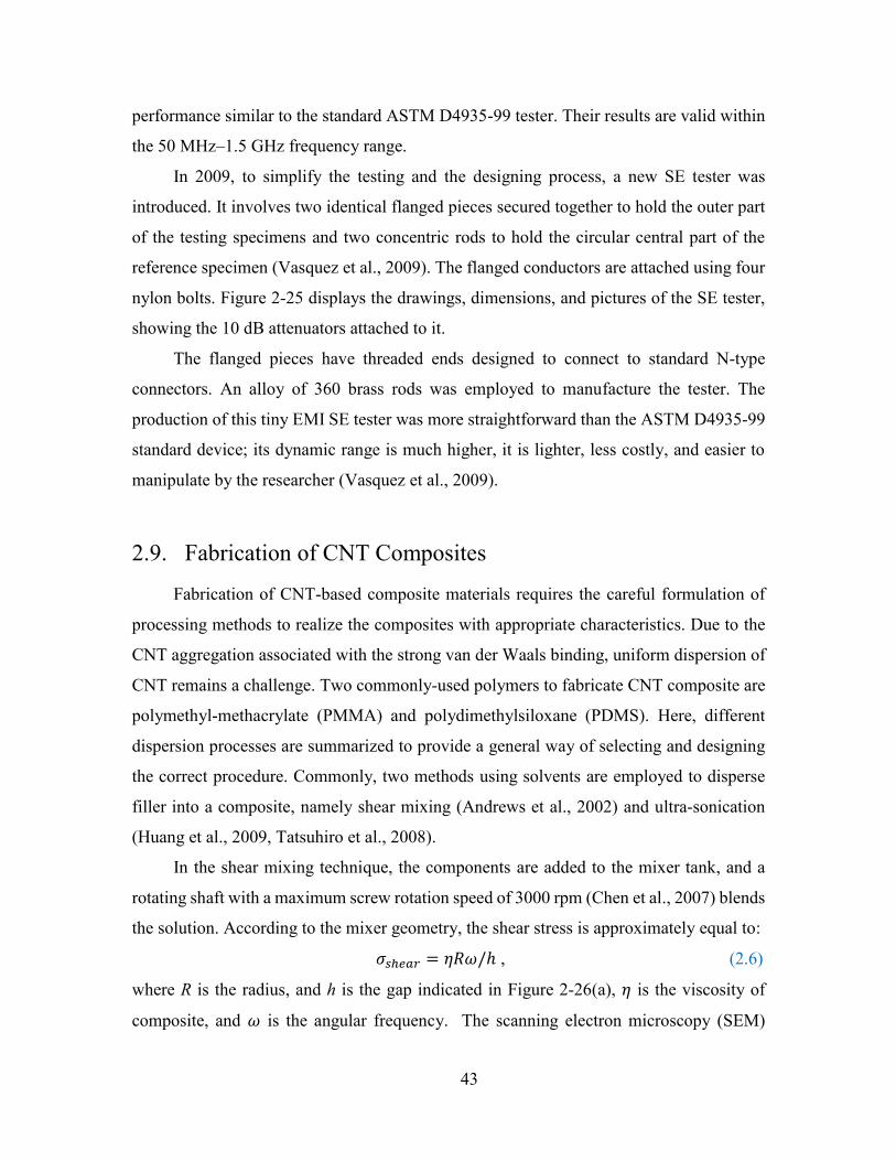
43
performance similar to the standard ASTM D4935-99 tester. Their results are valid within
the 50 MHz–1.5 GHz frequency range.
In 2009, to simplify the testing and the designing process, a new SE tester was
introduced. It involves two identical flanged pieces secured together to hold the outer part
of the testing specimens and two concentric rods to hold the circular central part of the
reference specimen (Vasquez et al., 2009). The flanged conductors are attached using four
nylon bolts. Figure 2-25 displays the drawings, dimensions, and pictures of the SE tester,
showing the 10 dB attenuators attached to it.
The flanged pieces have threaded ends designed to connect to standard N-type
connectors. An alloy of 360 brass rods was employed to manufacture the tester. The
production of this tiny EMI SE tester was more straightforward than the ASTM D4935-99
standard device; its dynamic range is much higher, it is lighter, less costly, and easier to
manipulate by the researcher (Vasquez et al., 2009).
2.9. Fabrication of CNT Composites
Fabrication of CNT-based composite materials requires the careful formulation of
processing methods to realize the composites with appropriate characteristics. Due to the
CNT aggregation associated with the strong van der Waals binding, uniform dispersion of
CNT remains a challenge. Two commonly-used polymers to fabricate CNT composite are
polymethyl-methacrylate (PMMA) and polydimethylsiloxane (PDMS). Here, different
dispersion processes are summarized to provide a general way of selecting and designing
the correct procedure. Commonly, two methods using solvents are employed to disperse
filler into a composite, namely shear mixing (Andrews et al., 2002) and ultra-sonication
(Huang et al., 2009, Tatsuhiro et al., 2008).
In the shear mixing technique, the components are added to the mixer tank, and a
rotating shaft with a maximum screw rotation speed of 3000 rpm (Chen et al., 2007) blends
the solution. According to the mixer geometry, the shear stress is approximately equal to:
𝜎𝑠ℎ𝑒𝑎𝑟 = 𝜂𝑅𝜔/ℎ , (2.6)
where R is the radius, and h is the gap indicated in Figure 2-26(a), 𝜂 is the viscosity of
composite, and 𝜔 is the angular frequency. The scanning electron microscopy (SEM)
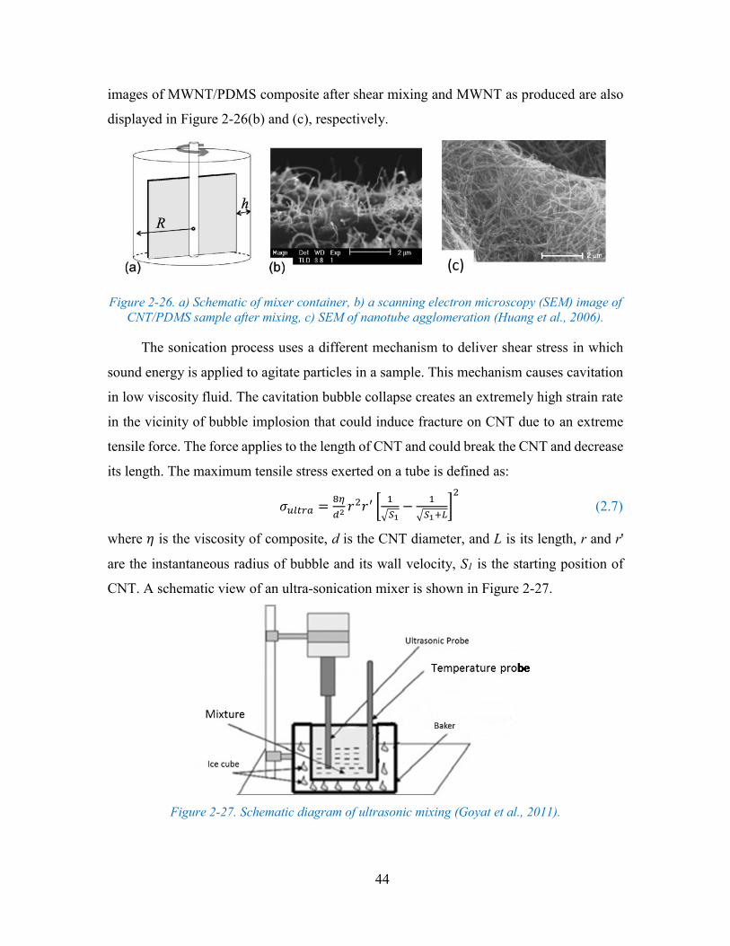
44
images of MWNT/PDMS composite after shear mixing and MWNT as produced are also
displayed in Figure 2-26(b) and (c), respectively.
Figure 2-26. a) Schematic of mixer container, b) a scanning electron microscopy (SEM) image of
CNT/PDMS sample after mixing, c) SEM of nanotube agglomeration (Huang et al., 2006).
The sonication process uses a different mechanism to deliver shear stress in which
sound energy is applied to agitate particles in a sample. This mechanism causes cavitation
in low viscosity fluid. The cavitation bubble collapse creates an extremely high strain rate
in the vicinity of bubble implosion that could induce fracture on CNT due to an extreme
tensile force. The force applies to the length of CNT and could break the CNT and decrease
its length. The maximum tensile stress exerted on a tube is defined as:
𝜎𝑢𝑙𝑡𝑟𝑎 =8𝜂
𝑑2 𝑟2𝑟′ [1
√𝑆1−
1
√𝑆1+𝐿]
2
(2.7)
where 𝜂 is the viscosity of composite, d is the CNT diameter, and L is its length, r and r'
are the instantaneous radius of bubble and its wall velocity, S1 is the starting position of
CNT. A schematic view of an ultra-sonication mixer is shown in Figure 2-27.
Figure 2-27. Schematic diagram of ultrasonic mixing (Goyat et al., 2011).
(c)
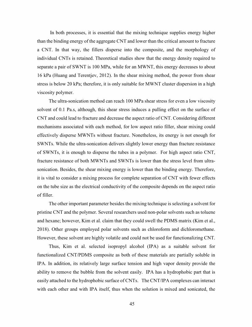
45
In both processes, it is essential that the mixing technique supplies energy higher
than the binding energy of the aggregate CNT and lower than the critical amount to fracture
a CNT. In that way, the fillers disperse into the composite, and the morphology of
individual CNTs is retained. Theoretical studies show that the energy density required to
separate a pair of SWNT is 100 MPa, while for an MWNT, this energy decreases to about
16 kPa (Huang and Terentjev, 2012). In the shear mixing method, the power from shear
stress is below 20 kPa; therefore, it is only suitable for MWNT cluster dispersion in a high
viscosity polymer.
The ultra-sonication method can reach 100 MPa shear stress for even a low viscosity
solvent of 0.1 Pa.s, although, this shear stress induces a pulling effect on the surface of
CNT and could lead to fracture and decrease the aspect ratio of CNT. Considering different
mechanisms associated with each method, for low aspect ratio filler, shear mixing could
effectively disperse MWNTs without fracture. Nonetheless, its energy is not enough for
SWNTs. While the ultra-sonication delivers slightly lower energy than fracture resistance
of SWNTs, it is enough to disperse the tubes in a polymer. For high aspect ratio CNT,
fracture resistance of both MWNTs and SWNTs is lower than the stress level from ultra-
sonication. Besides, the shear mixing energy is lower than the binding energy. Therefore,
it is vital to consider a mixing process for complete separation of CNT with fewer effects
on the tube size as the electrical conductivity of the composite depends on the aspect ratio
of filler.
The other important parameter besides the mixing technique is selecting a solvent for
pristine CNT and the polymer. Several researchers used non-polar solvents such as toluene
and hexane; however, Kim et al. claim that they could swell the PDMS matrix (Kim et al.,
2018). Other groups employed polar solvents such as chloroform and dichloromethane.
However, these solvent are highly volatile and could not be used for functionalizing CNT.
Thus, Kim et al. selected isopropyl alcohol (IPA) as a suitable solvent for
functionalized CNT/PDMS composite as both of these materials are partially soluble in
IPA. In addition, its relatively large surface tension and high vapor density provide the
ability to remove the bubble from the solvent easily. IPA has a hydrophobic part that is
easily attached to the hydrophobic surface of CNTs. The CNT/IPA complexes can interact
with each other and with IPA itself, thus when the solution is mixed and sonicated, the
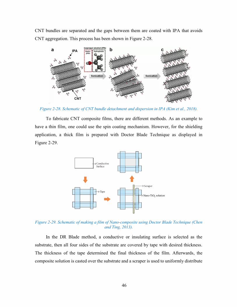
46
CNT bundles are separated and the gaps between them are coated with IPA that avoids
CNT aggregation. This process has been shown in Figure 2-28.
Figure 2-28. Schematic of CNT bundle detachment and dispersion in IPA (Kim et al., 2018).
To fabricate CNT composite films, there are different methods. As an example to
have a thin film, one could use the spin coating mechanism. However, for the shielding
application, a thick film is prepared with Doctor Blade Technique as displayed in
Figure 2-29.
Figure 2-29. Schematic of making a film of Nano-composite using Doctor Blade Technique (Chen
and Ting, 2013).
In the DR Blade method, a conductive or insulating surface is selected as the
substrate, then all four sides of the substrate are covered by tape with desired thickness.
The thickness of the tape determined the final thickness of the film. Afterwards, the
composite solution is casted over the substrate and a scraper is used to uniformly distribute
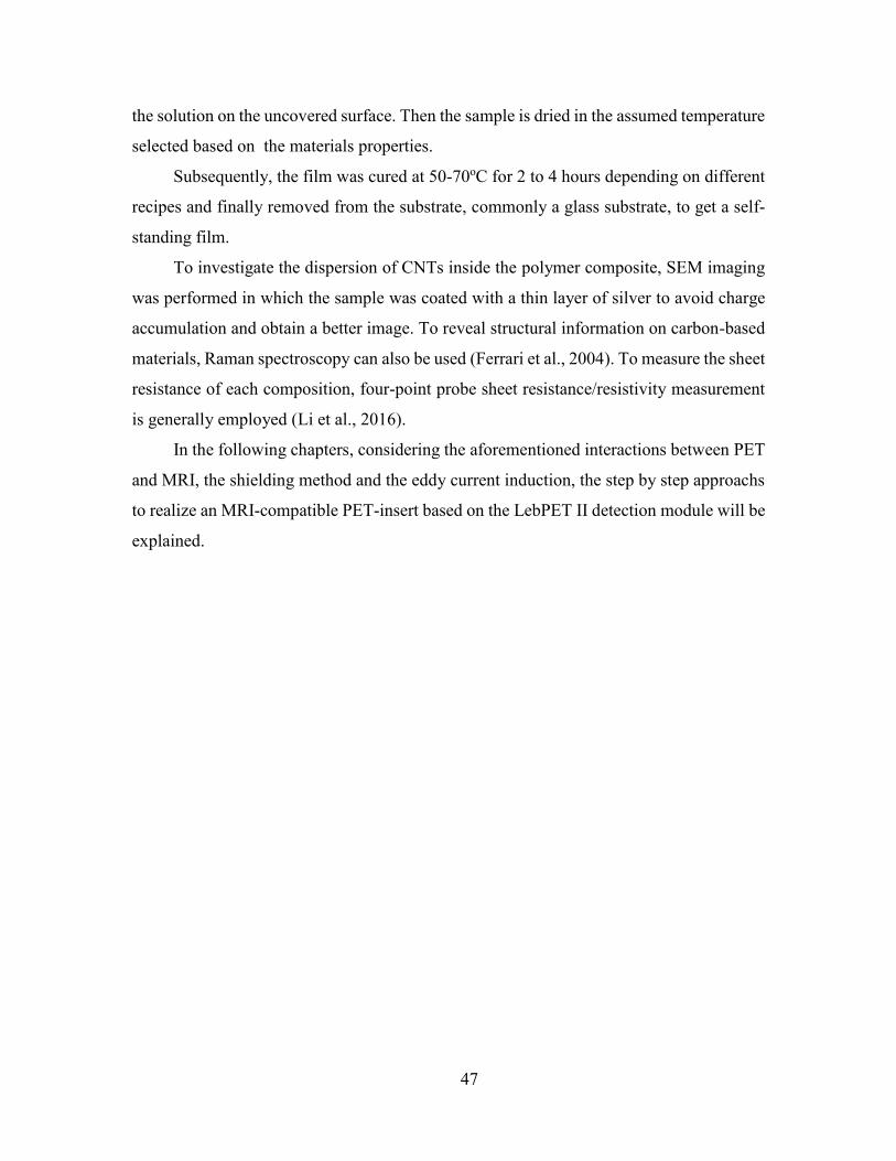
47
the solution on the uncovered surface. Then the sample is dried in the assumed temperature
selected based on the materials properties.
Subsequently, the film was cured at 50-70oC for 2 to 4 hours depending on different
recipes and finally removed from the substrate, commonly a glass substrate, to get a self-
standing film.
To investigate the dispersion of CNTs inside the polymer composite, SEM imaging
was performed in which the sample was coated with a thin layer of silver to avoid charge
accumulation and obtain a better image. To reveal structural information on carbon-based
materials, Raman spectroscopy can also be used (Ferrari et al., 2004). To measure the sheet
resistance of each composition, four-point probe sheet resistance/resistivity measurement
is generally employed (Li et al., 2016).
In the following chapters, considering the aforementioned interactions between PET
and MRI, the shielding method and the eddy current induction, the step by step approachs
to realize an MRI-compatible PET-insert based on the LebPET II detection module will be
explained.

48
49
CHAPTER 3
METALLIC MATERIAL EFFECTS
Avant-propos
Auteurs et Affiliation:
Narjes Moghadam: étudiante au doctorat, Institut interdisciplinaire
d’innovation technologique - 3IT, Université de Sherbrooke, Faculté de génie,
Département de génie électrique et de génie informatique.
Romain Espagnet : post-doctorant, Institut interdisciplinaire d’innovation
technologique - 3IT, Université de Sherbrooke, Faculté de génie, Département
de génie électrique et de génie informatique.
Jonathan Bouchard: étudiant au doctorat, Institut interdisciplinaire d’innovation
technologique - 3IT, Université de Sherbrooke, Faculté de génie, Département
de génie électrique et de génie informatique
Roger Lecomte: professeur, Université de Sherbrooke, Département de
médecine nucléaire et de radiobiologie
Réjean Fontaine: professeur, Institut interdisciplinaire d’innovation
technologique - 3IT, Université de Sherbrooke, Faculté de génie, Département
de génie électrique et de génie informatique.
Date d’acceptation : 29/01/2019
État de l’acceptation : Accepted, published on 21 March 2019, Phys Med Biol. 2019 Mar
21;64(7):075003. doi: 10.1088/1361-6560/ab0291
Revue : Physics in Medicine and Biology
Titre français : Étude des effets des composants métalliques de l'électronique TEP sur la
performance TEP et IRM sous excitation de gradients magnétiques
50
Contribution au document :
Cet article est le premier d’une série d’articles de la thèse qui discute des effets des
matériaux métalliques sur la performance TEP et IRM. Ce travail détermine si l'insertion
de pièces métalliques en dehors du champ de vue de l'IRM entre les bobines de gradients
magnétiques et la bobine RF peut perturber les performances de l'IRM ou de la TEP. Les
résultats théoriques et de simulation ont confirmé que les pièces métalliques
ferromagnétiques interagissaient avec les performances du scanner IRM et devaient être
complètement éliminées du champs de vue de l'IRM. Dans ce chapitre, nous avons
également abordé les aspects essentiels de la conception d’un module de détection TEP
compatible avec l’IRM du point de vue physique. Dans le chapitre suivant, nous
rapporterons les résultats expérimentaux de la performance des modules de détection
LabPET II en présence de bobines de l’IRM.
Résumé en français :
L'insertion d'un module de détection de tomographie d’émission par positrons (TEP)
à l’intérieur du champ de vue d'un IRM pose des problèmes en raison du comportement du
métal dans un champ magnétique variationnel puissant. Les matériaux métalliques, même
lorsque placés hors du champ de vue de l'IRM, pourraient non seulement perturber les
performances de l'IRM, mais aussi augmenter la température et les vibrations, entraînant
une faiblesse prématurée de l'électronique TEP. Pour étudier la compatibilité du module de
détection LabPET II à l’intérieur du champ IRM, cette publication présente une étude
théorique des artefacts induits par les métaux provenant de matériaux présents dans le
module de détection LabPET II. En outre, les effets des courants de Foucault et la perte de
chaleur associée sur le module de détection TEP, ont été examinés à l’aide de simulations
COMSOL. Les résultats montrent qu'en utilisant un module de détection LabPET II
modifié, l'artefact de déplacement provenant de l'introduction de petites quantités de métal
non ferromagnétique et les effets thermiques du métal en raison de la commutation de
gradient ont été respectivement compensés pour l'IRM et la TEP. Donc, le module de
détection LabPET II, avec quelques ajustements mineurs, serait compatible avec l'IRM
pour fonctionner efficacement à l'intérieur du champ d'un IRM sans perturber ses
performances.
51
Mots clés: TEP/IRM simultanée, Matériau métallique, Courant de Foucault,
Artéfacts de déplacement
Contribution of the document in the thesis (English):
This paper is the first paper of a series of articles explaining the first step to reach the
MR-compatible LabPET II detection module. This article contributes to this thesis by
providing a discussion on the effects of metallic materials on the performance of LabPET II
electronics and MRI. The goal was to find out whether inserting metallic parts outside the
field of view of MRI between gradient and RF coil could disturb the MRI performance or
even the LabPET II performance. The theoretical and simulation results confirmed that the
ferromagnetic metallic parts interact with both scanner performance and have to be
eliminated entirely from the MRI bore. In this chapter, we also discussed the essential
design considerations to have an MR-compatible LabPET II detection module from the
physics point of view. In the next section, we will report the experimental results of
LabPET II detection module performance in the presence of MRI coils.
*The text maybe different than the published verision, considering jury comments.
52
Studying the Effects of metallic
components of PET-insert on PET and
MRI performance due to gradient
switching
Abstract— Inserting positron emission tomography (PET) detection modules inside an
MRI bore imposes extra challenges owing to the behavior of metallic materials in a strong
magnetic field. The metallic parts, even when placed outside an MRI field of view, may
not only disturb MRI performance but could also increase temperature and vibrations,
leading to premature failure of PET electronics. To investigate the compatibility of
detection modules inside 3 T, 7 T and 9.4 T MRI bore, a theoretical study of the metal-
induced artifacts originating from component materials of the electronic circuit is
presented. The LabPET II detection module and a modified version of it in which the
connector was replaced by a ball grid array (BGA) were studied. In addition, the effect of
eddy current and the associated heat loss on the PET detection module have been examined
using COMSOL Multiphysics® simulations for 10 kHz and 100 kHz gradient switching.
Results show that displacement artifacts resulting from the presence of small amounts of
ferromagnetic metal and the heating effects of metal due to gradient switching can be
compensated by using the slightly modified LabPET II detection module. Thus, the
LabPET II system would be MR-compatible with some minor adjustments to operate
effectively inside an MRI bore without interfering with its performance.
Keywords: Simultaneous PET/MRI, Metallic material, Displacement artifacts, Eddy
current, Heat dissipation
53
3.1. Introduction
Advances in medical imaging, as well as high demand for more accurate and specific
data, have increased the interest to combine different imaging modalities for providing
images with enhanced quality and complementary functional and anatomical information
(Veit-Haibach et al., 2013). Simultaneous PET/MRI imaging allows both anatomical and
functional properties of tissues of interest to be revealed while preserving the spatial and
time correlation between the two different data sets. However, coupling any two different
electronics systems, such as Positron Emission Tomography (PET) and Magnetic
Resonance Imaging (MRI), introduces inevitable interferences due to their different nature
and most of the combined PET/MRI scanners designed for simultaneous operation
encounter challenges in the developing stage (Judenhofer et al., 2008, Pichler et al., 2010b,
Zaidi et al., 2011, Caldeira et al., 2018). Among those challenges, several interactions
between the two modalities must be addressed prior to reaching a fully functional PET/MRI
device (Vandenberghe and Marsden, 2015). Many research groups have reported these
interferences, including the impact of MRI on PET performance (Schlyer et al., 2007,
Weirich et al., 2012, Pichler et al., 2006) and the artifacts in MR images caused by the
PET-insert module (Wehrl et al., 2011, Yamamoto et al., 2011, Hong et al., 2013). Despite
those bottlenecks, the small animal LSO-APD based PET inserted in a 7 T MRI (Catana et
al., 2006) and a preclinical SiPM-based PET placed inside a 3 T MRI scanners have been
developed (Schulz et al., 2009) in 2006 and 2009 as first prototypes, respectively.
MRI has a strong magnetic field that is sensitive to materials’ magnetic susceptibility
(Yamamoto et al., 2002). Consequently, any material with different magnetic properties is
likely to cause inhomogeneities of the static magnetic field. Such distortions affect the
Larmor frequency and change the free induction decay (FID) signal from atoms, creating
a disturbance in the reconstruction of the MR image (Muzic and DiFilippo, 2014). In
addition to the main static magnetic field, three time-varying magnetic gradients enable the
extraction of the exact coordinates of a tissue of interest (spatial encoding). It is relevant to
mention that, based on Faraday’s law of induction, any variation in the magnetic field in
conductive materials induces eddy currents that generate heat dissipation. As a
consequence, a secondary magnetic field is created in the opposite direction of the initial
field, according to Lenz’s law, and disturbs the primary field (Delso and Ziegler, 2014).
54
For metallic parts positioned off the center of the MRI field-of-view (FOV), such as the
detection modules of a PET scanner, the eddy current induction is severe since the gradient
increases with distance from the MRI center. This, in turn, leads to a temperature increase
in the electromagnetically affected metallic parts as well as distortion of the initial gradient
fields. The resulting variation of the net magnetic field shifts the frequency associated with
the position, therefore generating an error in the detected position. Furthermore, the Larmor
frequency related to the main magnetic field of the MRI RF coil varies accordingly.
Nonetheless, the RF coil can be shielded using a conductive material and a good PCB
design technique. Since this subject has already been fully investigated (Peng et al., 2014a),
we will not discuss RF coil interferences with electronic boards in this paper.
Otherwise, some of the PET electronic components, for instance, capacitors, resistors,
and connectors contain ferromagnetic materials such as nickel or have a magnetic
susceptibility different from air. Thus, depending on their size, shape, position, orientation,
and distribution as well as their magnetic properties, these parts could contribute to
distortions of the magnetic field homogeneity (Starcukova et al., 2008). Regardless of the
susceptibility, the net magnetic field also changes because of the rapid variations of the
gradient magnetic field that induce a current in metallic parts. Such eddy currents pass
through the conductive loop, as an example the wirings, or the PCB power planes and, as
mentioned earlier, produce artifacts in MR images, as well as variations in the resonance
frequency (Hargreaves et al., 2011). This includes different displacement artifacts such as
geometric distortion, signal loss due to dephasing or pile-up. In fact, when the signal varies
spatially, it shifts away from its original region, causing signal loss, whereas its
accumulation in one region creates signal pile-up. Moreover, changes in actual position
and geometric distortion due to frequency variations are expected. Therefore, the issues
related to the metallic material present in PET electronics, especially its detection modules,
must be predominantly addressed prior to any simultaneous PET/MRI design.
Effects of metallic biomedical implants on MRI images have been widely investigated,
both experimentally (Shafiei et al., 2003, Costa et al., 2009) and theoretically (Sasaki et
al., 2013), and the artifacts from material magnetic susceptibility and eddy currents have
been observed. In this context, Bennett et al. reported artifacts produced by non-
ferromagnetic materials (Bennett et al., 1996), and Alanen et al. discussed the effect of
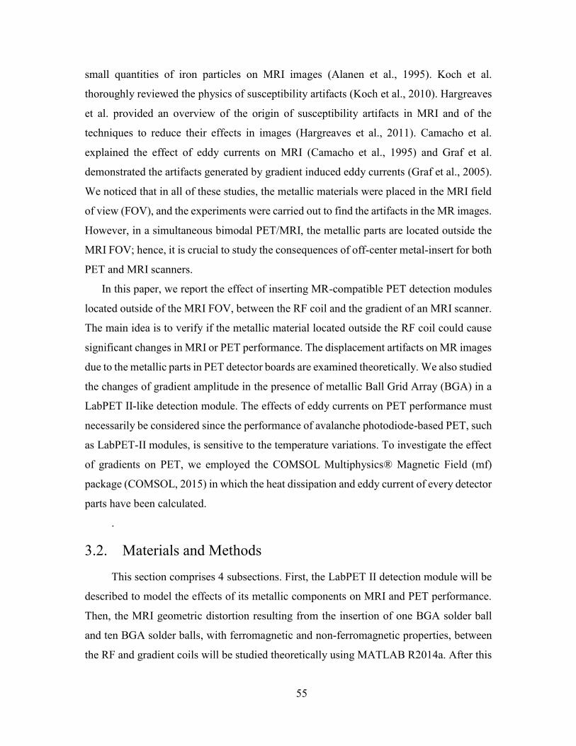
55
small quantities of iron particles on MRI images (Alanen et al., 1995). Koch et al.
thoroughly reviewed the physics of susceptibility artifacts (Koch et al., 2010). Hargreaves
et al. provided an overview of the origin of susceptibility artifacts in MRI and of the
techniques to reduce their effects in images (Hargreaves et al., 2011). Camacho et al.
explained the effect of eddy currents on MRI (Camacho et al., 1995) and Graf et al.
demonstrated the artifacts generated by gradient induced eddy currents (Graf et al., 2005).
We noticed that in all of these studies, the metallic materials were placed in the MRI field
of view (FOV), and the experiments were carried out to find the artifacts in the MR images.
However, in a simultaneous bimodal PET/MRI, the metallic parts are located outside the
MRI FOV; hence, it is crucial to study the consequences of off-center metal-insert for both
PET and MRI scanners.
In this paper, we report the effect of inserting MR-compatible PET detection modules
located outside of the MRI FOV, between the RF coil and the gradient of an MRI scanner.
The main idea is to verify if the metallic material located outside the RF coil could cause
significant changes in MRI or PET performance. The displacement artifacts on MR images
due to the metallic parts in PET detector boards are examined theoretically. We also studied
the changes of gradient amplitude in the presence of metallic Ball Grid Array (BGA) in a
LabPET II-like detection module. The effects of eddy currents on PET performance must
necessarily be considered since the performance of avalanche photodiode-based PET, such
as LabPET-II modules, is sensitive to the temperature variations. To investigate the effect
of gradients on PET, we employed the COMSOL Multiphysics® Magnetic Field (mf)
package (COMSOL, 2015) in which the heat dissipation and eddy current of every detector
parts have been calculated.
.
3.2. Materials and Methods
This section comprises 4 subsections. First, the LabPET II detection module will be
described to model the effects of its metallic components on MRI and PET performance.
Then, the MRI geometric distortion resulting from the insertion of one BGA solder ball
and ten BGA solder balls, with ferromagnetic and non-ferromagnetic properties, between
the RF and gradient coils will be studied theoretically using MATLAB R2014a. After this
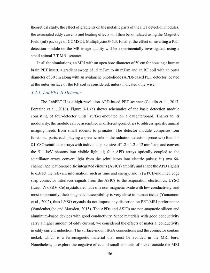
56
theoretical study, the effect of gradients on the metallic parts of the PET detection modules,
the associated eddy currents and heating effects will then be simulated using the Magnetic
Field (mf) package of COMSOL Multiphysics® 5.3. Finally, the effect of inserting a PET
detection module on the MR image quality will be experimentally investigated, using a
small animal 7 T MRI scanner.
In all the simulations, an MRI with an open bore diameter of 50 cm for housing a human
brain PET insert, a gradient sweep of 15 mT/m to 40 mT/m and an RF coil with an outer
diameter of 30 cm along with an avalanche photodiode (APD)-based PET detector located
at the outer surface of the RF coil is considered, unless indicated otherwise.
3.2.1. LabPET II Detector
The LabPET II is a high-resolution APD-based PET scanner (Gaudin et al., 2017,
Fontaine et al., 2016). Figure 3-1 (a) shows schematics of the basic detection module
consisting of four-detector units’ surface-mounted on a daughterboard. Thanks to its
modularity, the module can be assembled in different geometries to address specific animal
imaging needs from small rodents to primates. The detector module comprises four
functional parts, each playing a specific role in the radiation detection process: i) four 4 ×
8 LYSO scintillator arrays with individual pixel size of 1.2 × 1.2 × 12 mm3 stop and convert
the 511 keV photons into visible light; ii) four APD arrays optically coupled to the
scintillator arrays convert light from the scintillators into electric pulses; iii) two 64-
channel application-specific integrated circuits (ASICs) amplify and shape the APD signals
to extract the relevant information, such as time and energy; and iv) a PCB-mounted edge
strip connector interfaces signals from the ASICs to the acquisition electronics. LYSO
(Lu2(1-x)Y2xSiO5: Ce) crystals are made of a non-magnetic oxide with low conductivity, and
most importantly, their magnetic susceptibility is very close to human tissue (Yamamoto
et al., 2002), thus LYSO crystals do not impose any distortion on PET/MRI performance
(Vandenberghe and Marsden, 2015). The APDs and ASICs are non-magnetic silicon and
aluminum-based devices with good conductivity. Since materials with good conductivity
carry a higher amount of eddy current, we considered the effects of material conductivity
in eddy current induction. The surface-mount BGA connections and the connector contain
nickel, which is a ferromagnetic material that must be avoided in the MRI bore.
Nonetheless, to explore the negative effects of small amounts of nickel outside the MRI
57
FOV, as it would be the case for a PET-insert, the effects of ferromagnetic materials were
simulated. To eliminate the effects of these ferromagnetic materials, we also proposed
using a new connection method based on BGA made of 0.650 mm SAC305
(Sn96.5Ag3Cu0.5) solder balls. Besides the fact that it is the most standard ROHS (lead-free)
material for soldering, the SAC305 was selected for its non-ferromagnetic properties. Its
form factor when fully reflowed (size, shape, diameter, and height as a function of PCB
pad size) is well known (defined in IPC-7351B), and it provides good reliability at a low
cost (IPC, 2005).
The study also compares a single LabPET II detection module to a modified
module with the same size, herein called BGA-based detection module, consisting of an
FR4 substrate, two ASICs, eight 2 × 1 mils (known as 0201 component) passive SMD
components and 116 solder balls. The BGA-based detection module is displayed in Figure
3-1 (b). The only remaining ferromagnetic parts in the latter device are located in the lead
plating of SMD components containing 15 µg of nickel each, based on the supplier
Composition Sheet (Murata, 2018) This insignificant amount of nickel should have a
negligible effect in comparison to a bulk nickel-based connector or even a nickel-plated
ball with 0.650 mm diameter. In the simulation, we did not consider the nickel plating of
the SMD parts, as it is almost 100 times smaller in size than one BGA ball. Assuming that
the other properties would be the same, the results would simply be scaled down by a factor
of (1/100)3.
Figure 3-1 a) The LabPET II Detector module, b) the MR-compatible BGA-based detection
module under study
58
3.2.2. Field Inhomogeneity and Geometric Distortion Theory
The type and the strength of metallic artifacts such as displacement depend on the
applied MRI sequences. To avoid dephasing effects, in a theoretical study of image
coordinate distortion, we used a spin-echo sequence in which both slice and readout
selection change with the magnetic field (Hargreaves et al., 2011). Figure 3-2 shows the
cylindrical coordinate employed in our simulations. The actual coordinates of the imaging
tissue are (x, y, z), the reconstructed coordinates in the image are (x’, y’, z’), and the PET
detector is located at (x”, y”, z”) = (R, θ, z”), where 𝑅 = √𝑥2 + 𝑦2 and 𝜃 = tan−1(𝑦
𝑥) =
0, (unless otherwise mentioned). Here, the z coordinate is used for slice selection, the x
coordinate is for readout encoding, and the y coordinate is for phase encoding.
Figure 3-2. Cylindrical-coordinate using for simulation, a purple circle shows a coordinate of
one detection module
Considering the main magnetic field as B0, the Gradient magnetic field as BG(r) and
the metallic part’s magnetic field as BM(r), the magnetic field of metallic parts is calculated
using:
𝐵0 = 𝐵0â𝑧 (3.1)
𝐵𝐺(𝑟) = (𝐺𝑥. 𝑥 + 𝐺𝑦. 𝑦 + 𝐺𝑧 . 𝑧)â𝑧 (3.2)
𝐵𝑀(𝑟) = ( 3𝑟(𝑚.𝑟′)−𝑚(𝑟′)3
(𝑟′)5) = (𝐵𝑀𝑥�̂�𝑥, 𝐵𝑀𝑦�̂�𝑦, 𝐵𝑀𝑧�̂�𝑧) (3.3)
where m is the dipole moment equals to 𝜒𝑉𝐵0 in which χ is the susceptibility of material,
V is the volume of material as well Gx, Gy, and Gz are selected to have a gradient of 40
mT/m or less. The coordinate 𝑟′ indicates the distance of the imaging region from the metal.
The magnetic susceptibility of materials used in this simulation is summarized in Table 3-1.
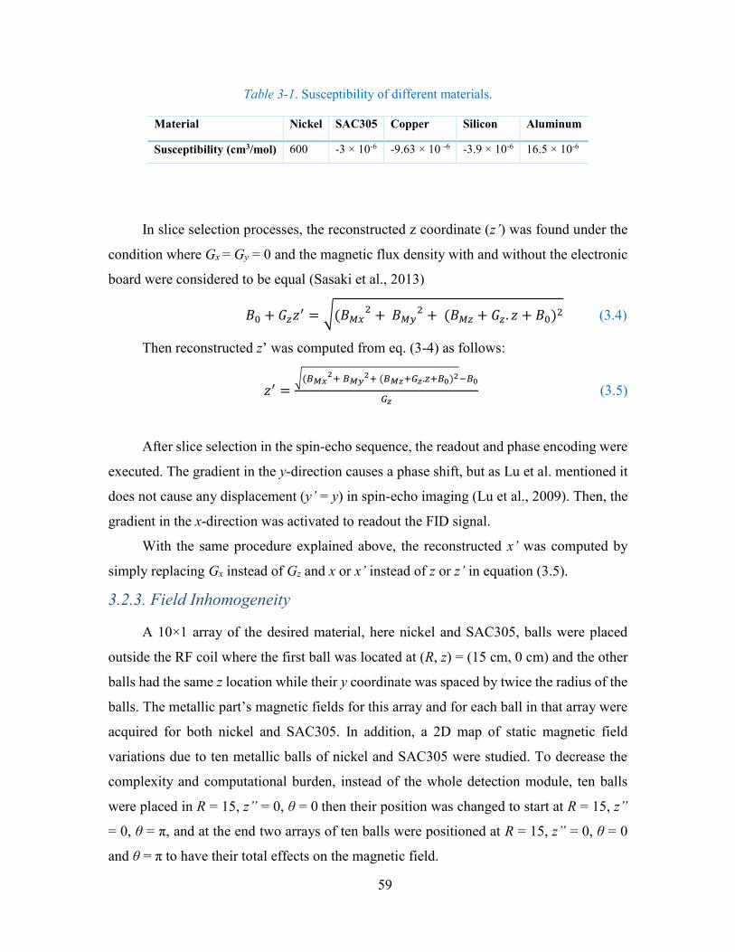
59
Table 3-1. Susceptibility of different materials.
Material Nickel SAC305 Copper Silicon Aluminum
Susceptibility (cm3/mol) 600 -3 × 10⁻⁶ -9.63 × 10 -6 -3.9 × 10⁻⁶ 16.5 × 10⁻⁶
In slice selection processes, the reconstructed z coordinate (z’) was found under the
condition where Gx = Gy = 0 and the magnetic flux density with and without the electronic
board were considered to be equal (Sasaki et al., 2013)
𝐵0 + 𝐺𝑧𝑧′ = √(𝐵𝑀𝑥2 + 𝐵𝑀𝑦
2 + (𝐵𝑀𝑧 + 𝐺𝑧 . 𝑧 + 𝐵0)2 (3.4)
Then reconstructed z’ was computed from eq. (3-4) as follows:
𝑧′ =√(𝐵𝑀𝑥
2+ 𝐵𝑀𝑦2+ (𝐵𝑀𝑧+𝐺𝑧.𝑧+𝐵0)2−𝐵0
𝐺𝑧 (3.5)
After slice selection in the spin-echo sequence, the readout and phase encoding were
executed. The gradient in the y-direction causes a phase shift, but as Lu et al. mentioned it
does not cause any displacement (y’ = y) in spin-echo imaging (Lu et al., 2009). Then, the
gradient in the x-direction was activated to readout the FID signal.
With the same procedure explained above, the reconstructed x’ was computed by
simply replacing Gx instead of Gz and x or x’ instead of z or z’ in equation (3.5).
3.2.3. Field Inhomogeneity
A 10×1 array of the desired material, here nickel and SAC305, balls were placed
outside the RF coil where the first ball was located at (R, z) = (15 cm, 0 cm) and the other
balls had the same z location while their y coordinate was spaced by twice the radius of the
balls. The metallic part’s magnetic fields for this array and for each ball in that array were
acquired for both nickel and SAC305. In addition, a 2D map of static magnetic field
variations due to ten metallic balls of nickel and SAC305 were studied. To decrease the
complexity and computational burden, instead of the whole detection module, ten balls
were placed in R = 15, z” = 0, θ = 0 then their position was changed to start at R = 15, z”
= 0, θ = π, and at the end two arrays of ten balls were positioned at R = 15, z” = 0, θ = 0
and θ = π to have their total effects on the magnetic field.
60
3.2.4. Geometric Distortion
The geometric distortion effects have been surveyed for one ball at a different place
and an array of ten balls.
One-Ball Simulation. Based on the above theory, the effect of inserting one
solder ball of ferromagnetic material (nickel with susceptibility of 600 (SI)) with a 0.325
mm radius in the isocenter of the 3 T MRI scanner was studied. Next, the ferromagnetic
solder ball was moved outside of MRI FOV at coordinate (R, z) = (15, 0) cm with the angle
deviation of θ = 0 and θ = π to observe the effect of metal on the z coordinate. We also
studied the effect of different slice selection by selecting z = ±1 cm from the MRI center.
Once again, one ball of SAC305 was inserted in (R, z) = (15, 0) cm with both angles of θ
= 0 and θ = π. In this case, the effect of different slice selection (z) was also examined for
z = ± 1 cm from the center. The magnetic field was selected at 3 T, and the gradient change
was 40 mT/m.
Ten-Ball Array Simulation. The same array described in section 3.2.3 was used
to determine the displacement effects. Using this array, the effects of the ball number on
the displacement of position were studied. Magnetic field strengths of 3 T, 7 T, and 9.4 T
with 40 mT/m gradient were used with ferromagnetic ball. For the SAC305 ball same
magnetic field with gradient field variation of 40, 30, 20 and 15 mT/m were studied.
3.3. Eddy Current and Heat Dissipation Simulation
After studying the effects of metallic parts on the MRI image, the next step was to
simulate the effect of the MR and gradient fields on the PET detection module placed
outside the MRI FOV. Both the LabPET II module with a nickel-connector and the BGA-
based one were investigated. For this purpose, the COMSOL Magnetic Field Physics (mf)
package was used.
To reduce the computational burden, the full gradient coil set-up was replaced by a
frequency-dependent current passing through a wire. In addition, to simplify the
simulation, the connector was modeled as a simple rectangular filled with a composite of
plastic and nickel with volume rather than a fully described component. The PET detection
61
module was placed at 15 cm away from the center at z = 0, θ = 0 with the detection module
aligned along the z-axis to assess the highest impact of gradient changes. The ASIC of both
detection modules were plated with copper to investigate the worst-case situation, while
the substrate was selected as FR4 epoxy. Solder balls were spheres of SAC305. The
LabPET II detection module with a nickel connector was also simulated to have a criterion
to compare and to assess the advantage of the proposed new design as well as to establish
tangible design considerations. For both modules, we examined the eddy current effects on
their performance and heat dissipation. Two gradient frequencies of 10 kHz and 100 kHz
were selected as the fundamental frequencies of the gradient driver (Lai et al., 2011). To
find out the magnetic flux density due to those gradient fields and calculate the eddy current
and heat dissipation, COMSOL uses the magnetic vector potential (A) that can be
calculated from the following equation:
(𝑗𝜔𝜎 − 𝜔2𝜀)𝐴 + ∇ × (1
𝜇∇ × 𝐴) = 0 (3.6)
where σ is the conductivity, ε the permittivity, and μ the permeability.
The skin depth (δ) of material is required to model the eddy current in COMSOL
Multiphysics®. The skin depth of copper and SAC305 is shown in Table 3-2 for 10 kHz
and 100 kHz. In order to resolve the evanescent field in the metal, the mesh size was
defined according to these skin depths. Here, the maximum mesh size for BGA was
selected to be 0.05 mm. The power dissipation in conductors can be calculated using the
specialized Multiphysics Interface for Joule heating embedded in COMSOL. For the
LabPET II connector, we considered it as a mixed material containing nickel, copper, and
plastic with an equal composition of each rather than a pure ferromagnetic bulk and we
then applied the same physical concepts as for copper.
Table 3-2. Skin depth of copper and SAC305 at 100 kHz and 10 kHz
10 kHz 100 kHz
Copper 0.651 mm 0.206 mm
SAC305 1.64 mm 0.517 mm
Having the current density and volumetric heat dissipation, we calculated the net
current and heat dissipation by integration over the volume of the detector. The eddy
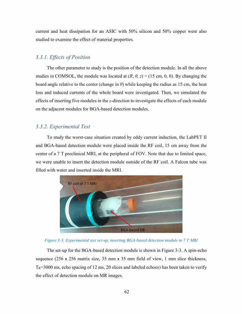
62
current and heat dissipation for an ASIC with 50% silicon and 50% copper were also
studied to examine the effect of material properties.
3.3.1. Effects of Position
The other parameter to study is the position of the detection module. In all the above
studies in COMSOL, the module was located at (R, θ, z) = (15 cm, 0, 0). By changing the
board angle relative to the center (change in θ) while keeping the radius as 15 cm, the heat
loss and induced currents of the whole board were investigated. Then, we simulated the
effects of inserting five modules in the z-direction to investigate the effects of each module
on the adjacent modules for BGA-based detection modules.
3.3.2. Experimental Test
To study the worst-case situation created by eddy current induction, the LabPET II
and BGA-based detection module were placed inside the RF coil, 15 cm away from the
center of a 7 T preclinical MRI, at the peripheral of FOV. Note that due to limited space,
we were unable to insert the detection module outside of the RF coil. A Falcon tube was
filled with water and inserted inside the MRI.
Figure 3-3. Experimental test set-up, inserting BGA-based detection module in 7 T MRI
The set-up for the BGA-based detection module is shown in Figure 3-3. A spin-echo
sequence (256 x 256 matrix size, 35 mm x 35 mm field of view, 1 mm slice thickness,
TR=3000 ms, echo spacing of 12 ms, 20 slices and labeled echoes) has been taken to verify
the effect of detection module on MR images.
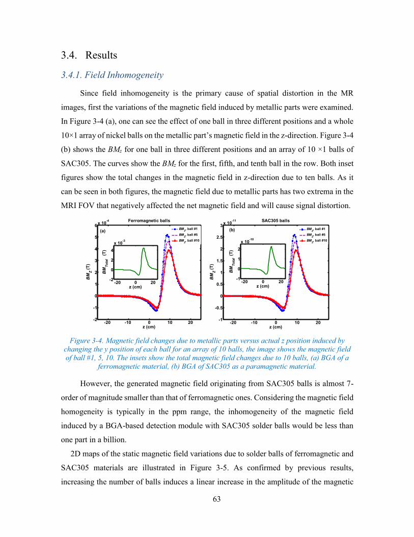
63
3.4. Results
3.4.1. Field Inhomogeneity
Since field inhomogeneity is the primary cause of spatial distortion in the MR
images, first the variations of the magnetic field induced by metallic parts were examined.
In Figure 3-4 (a), one can see the effect of one ball in three different positions and a whole
10×1 array of nickel balls on the metallic part’s magnetic field in the z-direction. Figure 3-4
(b) shows the BMz for one ball in three different positions and an array of 10 ×1 balls of
SAC305. The curves show the BMz for the first, fifth, and tenth ball in the row. Both inset
figures show the total changes in the magnetic field in z-direction due to ten balls. As it
can be seen in both figures, the magnetic field due to metallic parts has two extrema in the
MRI FOV that negatively affected the net magnetic field and will cause signal distortion.
Figure 3-4. Magnetic field changes due to metallic parts versus actual z position induced by
changing the y position of each ball for an array of 10 balls, the image shows the magnetic field
of ball #1, 5, 10. The insets show the total magnetic field changes due to 10 balls, (a) BGA of a
ferromagnetic material, (b) BGA of SAC305 as a paramagnetic material.
However, the generated magnetic field originating from SAC305 balls is almost 7-
order of magnitude smaller than that of ferromagnetic ones. Considering the magnetic field
homogeneity is typically in the ppm range, the inhomogeneity of the magnetic field
induced by a BGA-based detection module with SAC305 solder balls would be less than
one part in a billion.
2D maps of the static magnetic field variations due to solder balls of ferromagnetic and
SAC305 materials are illustrated in Figure 3-5. As confirmed by previous results,
increasing the number of balls induces a linear increase in the amplitude of the magnetic
-20 -10 0 10 20-1
-0.5
0
0.5
1
1.5
2
2.5
3x 10
-11
z (cm)
BM
Z (
T)
SAC305 balls
-20 0 20-1
0
1
2
x 10-10
z (cm)
BM
To
tal
(T)
-20 -10 0 10 20-2
-1
0
1
2
3
4
5
6x 10
-4
z (cm)
BM
Z (
T)
Ferromagnetic balls
-20 0 20-2
0
2
4
x 10-3
z (cm)
BM
To
tal
(T
)
BMZ, ball #1
BMZ, ball #5
BMZ, ball #10
BMZ, ball #1
BMZ, ball #5
BMZ, ball #10
(b)(a)
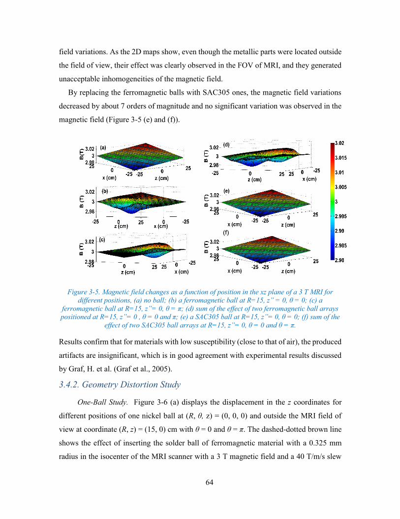
64
field variations. As the 2D maps show, even though the metallic parts were located outside
the field of view, their effect was clearly observed in the FOV of MRI, and they generated
unacceptable inhomogeneities of the magnetic field.
By replacing the ferromagnetic balls with SAC305 ones, the magnetic field variations
decreased by about 7 orders of magnitude and no significant variation was observed in the
magnetic field (Figure 3-5 (e) and (f)).
Figure 3-5. Magnetic field changes as a function of position in the xz plane of a 3 T MRI for
different positions, (a) no ball; (b) a ferromagnetic ball at R=15, z” = 0, θ = 0; (c) a
ferromagnetic ball at R=15, z”= 0, θ = π; (d) sum of the effect of two ferromagnetic ball arrays
positioned at R=15, z”= 0 , θ = 0 and π; (e) a SAC305 ball at R=15, z”= 0, θ = 0; (f) sum of the
effect of two SAC305 ball arrays at R=15, z”= 0, θ = 0 and θ = π.
Results confirm that for materials with low susceptibility (close to that of air), the produced
artifacts are insignificant, which is in good agreement with experimental results discussed
by Graf, H. et al. (Graf et al., 2005).
3.4.2. Geometry Distortion Study
One-Ball Study. Figure 3-6 (a) displays the displacement in the z coordinates for
different positions of one nickel ball at (R, θ, z) = (0, 0, 0) and outside the MRI field of
view at coordinate (R, z) = (15, 0) cm with θ = 0 and θ = π. The dashed-dotted brown line
shows the effect of inserting the solder ball of ferromagnetic material with a 0.325 mm
radius in the isocenter of the MRI scanner with a 3 T magnetic field and a 40 T/m/s slew
(f)
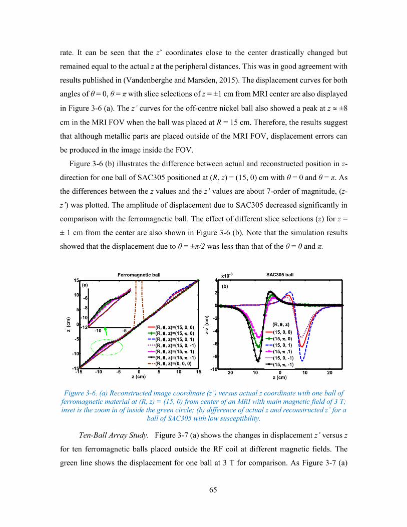
65
rate. It can be seen that the z’ coordinates close to the center drastically changed but
remained equal to the actual z at the peripheral distances. This was in good agreement with
results published in (Vandenberghe and Marsden, 2015). The displacement curves for both
angles of θ = 0, θ = π with slice selections of z = ±1 cm from MRI center are also displayed
in Figure 3-6 (a). The z’ curves for the off-centre nickel ball also showed a peak at z ±8
cm in the MRI FOV when the ball was placed at R = 15 cm. Therefore, the results suggest
that although metallic parts are placed outside of the MRI FOV, displacement errors can
be produced in the image inside the FOV.
Figure 3-6 (b) illustrates the difference between actual and reconstructed position in z-
direction for one ball of SAC305 positioned at (R, z) = (15, 0) cm with θ = 0 and θ = π. As
the differences between the z values and the z’ values are about 7-order of magnitude, (z-
z’) was plotted. The amplitude of displacement due to SAC305 decreased significantly in
comparison with the ferromagnetic ball. The effect of different slice selections (z) for z =
± 1 cm from the center are also shown in Figure 3-6 (b). Note that the simulation results
showed that the displacement due to θ = ±π/2 was less than that of the θ = 0 and π.
Figure 3-6. (a) Reconstructed image coordinate (z’) versus actual z coordinate with one ball of
ferromagnetic material at (R, z) = (15, 0) from center of an MRI with main magnetic field of 3 T;
inset is the zoom in of inside the green circle; (b) difference of actual z and reconstructed z’ for a
ball of SAC305 with low susceptibility.
Ten-Ball Array Study. Figure 3-7 (a) shows the changes in displacement z’ versus z
for ten ferromagnetic balls placed outside the RF coil at different magnetic fields. The
green line shows the displacement for one ball at 3 T for comparison. As Figure 3-7 (a)
-15 -10 -5 0 5 10 15-15
-10
-5
0
5
10
15Ferromagnetic ball
z (cm)
z' (
cm
)
(R, , z)=(15, 0, 0)
(R, , z)=(15, , 0)
(R, , z)=(15, 0, 1)
(R, , z)=(15, 0, -1)
(R, , z)=(15, , 1)
(R, , z)=(15, , -1)
(R, , z)=(0, 0, 0)
20 10 0 10 20-10
-8
-6
-4
-2
0
2
4
z (cm)
z-z
' (cm
)
SAC305 ball
(15, 0, 0)
(15, , 0)
(15, 0, 1)
(15, ,1)
(15, 0, -1)
(15, , -1)
-10 -5-12
-10
-8
-6
x10-8
(R, , z)
(b)(a)
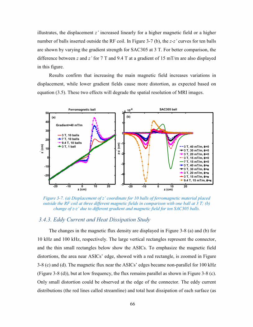
66
illustrates, the displacement z’ increased linearly for a higher magnetic field or a higher
number of balls inserted outside the RF coil. In Figure 3-7 (b), the z-z’ curves for ten balls
are shown by varying the gradient strength for SAC305 at 3 T. For better comparison, the
difference between z and z’ for 7 T and 9.4 T at a gradient of 15 mT/m are also displayed
in this figure.
Results confirm that increasing the main magnetic field increases variations in
displacement, while lower gradient fields cause more distortion, as expected based on
equation (3.5). These two effects will degrade the spatial resolution of MRI images.
Figure 3-7. (a) Displacement of z’ coordinate for 10 balls of ferromagnetic material placed
outside the RF coil at three different magnetic fields in comparison with one ball at 3 T; (b)
change of z-z’ due to different gradient and magnetic field for ten SAC305 balls.
3.4.3. Eddy Current and Heat Dissipation Study
The changes in the magnetic flux density are displayed in Figure 3-8 (a) and (b) for
10 kHz and 100 kHz, respectively. The large vertical rectangles represent the connector,
and the thin small rectangles below show the ASICs. To emphasize the magnetic field
distortions, the area near ASICs’ edge, showed with a red rectangle, is zoomed in Figure
3-8 (c) and (d). The magnetic flux near the ASICs’ edges became non-parallel for 100 kHz
(Figure 3-8 (d)), but at low frequency, the flux remains parallel as shown in Figure 3-8 (c).
Only small distortion could be observed at the edge of the connector. The eddy current
distributions (the red lines called streamline) and total heat dissipation of each surface (as
-20 -10 0 10 20-5
-4
-3
-2
-1
0
1
2x 10
-8
z (cm)
z-z
' (c
m)
SAC305 ball
3 T, 40 mT/m, =0
3 T, 30 mT/m, =0
3 T, 20 mT/m, =0
3 T, 15 mT/m, =0
7 T, 15 mT/m, =0
3 T, 40 mT/m, =
3 T, 30 mT/m, =
3 T, 20 mT/m, =
3 T, 15 mT/m, =
9.4 T, 15 mT/m, =
-20 -10 0 10 20
-20
-10
0
10
20
30
40
50
z (cm)
z' (
cm
)
Ferromagnetic ball
3 T, 10 balls
7 T, 10 balls
9.4 T, 10 balls
3 T, 1 ball
Gradient=40 mT/m
(b)(a)
10-6
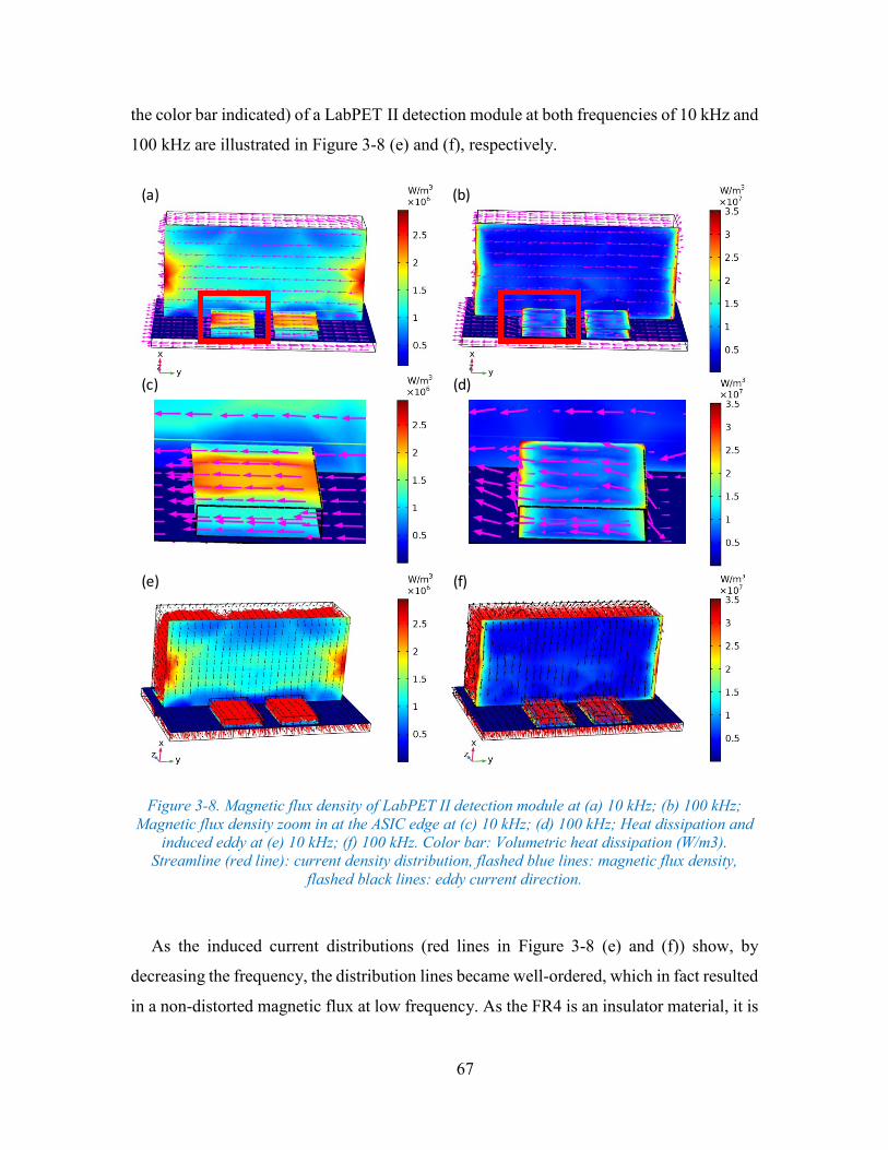
67
the color bar indicated) of a LabPET II detection module at both frequencies of 10 kHz and
100 kHz are illustrated in Figure 3-8 (e) and (f), respectively.
Figure 3-8. Magnetic flux density of LabPET II detection module at (a) 10 kHz; (b) 100 kHz;
Magnetic flux density zoom in at the ASIC edge at (c) 10 kHz; (d) 100 kHz; Heat dissipation and
induced eddy at (e) 10 kHz; (f) 100 kHz. Color bar: Volumetric heat dissipation (W/m3).
Streamline (red line): current density distribution, flashed blue lines: magnetic flux density,
flashed black lines: eddy current direction.
As the induced current distributions (red lines in Figure 3-8 (e) and (f)) show, by
decreasing the frequency, the distribution lines became well-ordered, which in fact resulted
in a non-distorted magnetic flux at low frequency. As the FR4 is an insulator material, it is
(a) (b)
(c) (d)
(e) (f)
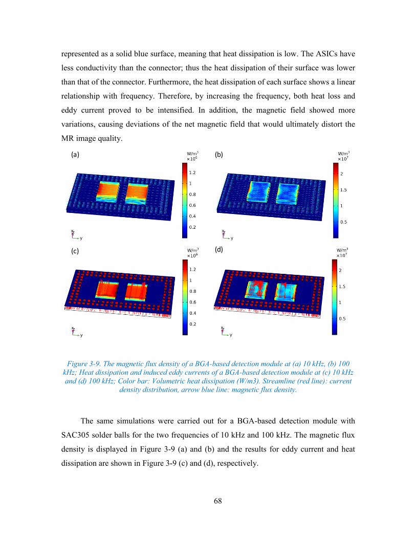
68
represented as a solid blue surface, meaning that heat dissipation is low. The ASICs have
less conductivity than the connector; thus the heat dissipation of their surface was lower
than that of the connector. Furthermore, the heat dissipation of each surface shows a linear
relationship with frequency. Therefore, by increasing the frequency, both heat loss and
eddy current proved to be intensified. In addition, the magnetic field showed more
variations, causing deviations of the net magnetic field that would ultimately distort the
MR image quality.
Figure 3-9. The magnetic flux density of a BGA-based detection module at (a) 10 kHz, (b) 100
kHz; Heat dissipation and induced eddy currents of a BGA-based detection module at (c) 10 kHz
and (d) 100 kHz; Color bar: Volumetric heat dissipation (W/m3). Streamline (red line): current
density distribution, arrow blue line: magnetic flux density.
The same simulations were carried out for a BGA-based detection module with
SAC305 solder balls for the two frequencies of 10 kHz and 100 kHz. The magnetic flux
density is displayed in Figure 3-9 (a) and (b) and the results for eddy current and heat
dissipation are shown in Figure 3-9 (c) and (d), respectively.
(a) (b)
(c) (d)
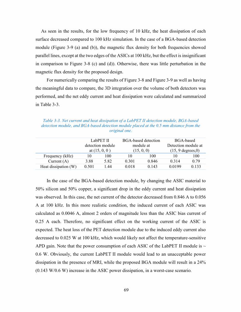
69
As seen in the results, for the low frequency of 10 kHz, the heat dissipation of each
surface decreased compared to 100 kHz simulation. In the case of a BGA-based detection
module (Figure 3-9 (a) and (b)), the magnetic flux density for both frequencies showed
parallel lines, except at the two edges of the ASICs at 100 kHz, but the effect is insignificant
in comparison to Figure 3-8 (c) and (d)). Otherwise, there was little perturbation in the
magnetic flux density for the proposed design.
For numerically comparing the results of Figure 3-8 and Figure 3-9 as well as having
the meaningful data to compare, the 3D integration over the volume of both detectors was
performed, and the net eddy current and heat dissipation were calculated and summarized
in Table 3-3.
Table 3-3. Net current and heat dissipation of a LabPET II detection module, BGA-based
detection module, and BGA-based detection module placed at the 0.5 mm distance from the
original one.
LabPET II
detection module
at (15, 0, 0 )
BGA-based detection
module at
(15, 0, 0)
BGA-based
Detection module at
(15, 9 degrees,0)
Frequency (kHz) 10 100 10 100 10 100
Current (A) 3.88 5.82 0.301 0.846 0.314 0.79
Heat dissipation (W) 0.501 1.44 0.018 0.143 0.0199 0.133
In the case of the BGA-based detection module, by changing the ASIC material to
50% silicon and 50% copper, a significant drop in the eddy current and heat dissipation
was observed. In this case, the net current of the detector decreased from 0.846 A to 0.056
A at 100 kHz. In this more realistic condition, the induced current of each ASIC was
calculated as 0.0046 A, almost 2 orders of magnitude less than the ASIC bias current of
0.25 A each. Therefore, no significant effect on the working current of the ASIC is
expected. The heat loss of the PET detection module due to the induced eddy current also
decreased to 0.025 W at 100 kHz, which would likely not affect the temperature-sensitive
APD gain. Note that the power consumption of each ASIC of the LabPET II module is ~
0.6 W. Obviously, the current LabPET II module would lead to an unacceptable power
dissipation in the presence of MRI, while the proposed BGA module will result in a 24%
(0.143 W/0.6 W) increase in the ASIC power dissipation, in a worst-case scenario.
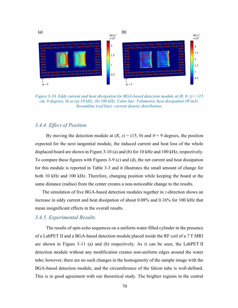
70
Figure 3-10. Eddy current and heat dissipation for BGA-based detection module at (R, θ, z) = (15
cm, 9 degrees, 0) at (a) 10 kHz, (b) 100 kHz. Color bar: Volumetric heat dissipation (W/m3).
Streamline (red line): current density distribution.
3.4.4. Effect of Position
By moving the detection module at (R, z) = (15, 0) and θ = 9 degrees, the position
expected for the next tangential module, the induced current and heat loss of the whole
displaced board are shown in Figure 3-10 (a) and (b) for 10 kHz and 100 kHz, respectively.
To compare these figures with Figures 3-9 (c) and (d), the net current and heat dissipation
for this module is reported in Table 3-3 and it illustrates the small amount of change for
both 10 kHz and 100 kHz. Therefore, changing position while keeping the board at the
same distance (radius) from the center creates a non-noticeable change to the results.
The simulation of five BGA-based detection modules together in z-direction shows an
increase in eddy current and heat dissipation of about 0.08% and 0.16% for 100 kHz that
mean insignificant effects in the overall results.
3.4.5. Experimental Results
The results of spin-echo sequences on a uniform water-filled cylinder in the presence
of a LabPET II and a BGA-based detection module placed inside the RF coil of a 7 T MRI
are shown in Figure 3-11 (a) and (b) respectively. As it can be seen, the LabPET II
detection module without any modification creates non-uniform edges around the water
tube; however, there are no such changes in the homogeneity of the sample image with the
BGA-based detection module, and the circumference of the falcon tube is well-defined.
This is in good agreement with our theoretical study. The brighter regions in the central
(a) (b)
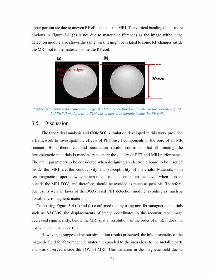
71
upper portion are due to uneven RF effect inside the MRI. The vertical banding that is more
obvious in Figure 3-11(b) is not due to material differences as the image without the
detection module also shows the same lines. It might be related to some RF changes inside
the MRI, not to the material inside the RF coil.
Figure 3-11. Spin echo sequences image of a falcon tube filled with water in the presence of (a)
LabPET II module, (b) a BGA-based detection module inside the RF coil.
3.5. Discussion
The theoretical analysis and COMSOL simulation developed in this work provided
a framework to investigate the effects of PET insert components in the bore of an MR
scanner. Both theoretical and simulation results confirmed that eliminating the
ferromagnetic materials is mandatory to spare the quality of PET and MRI performance.
The main parameters to be considered when designing an electronic board to be inserted
inside the MRI are the conductivity and susceptibility of materials. Materials with
ferromagnetic properties were shown to cause displacement artifacts even when inserted
outside the MRI FOV, and therefore, should be avoided as much as possible. Therefore,
our results were in favor of the BGA-based PET detection module, avoiding as much as
possible ferromagnetic materials.
Comparing Figure 3-4 (a) and (b) confirmed that by using non-ferromagnetic materials
such as SAC305, the displacements of image coordinates in the reconstructed image
decreased significantly, below the MRI spatial resolution (of the order of mm), it does not
create a displacement error.
However, as suggested by our simulation results presented, the inhomogeneity of the
magnetic field for ferromagnetic material expanded to the area close to the metallic parts
and was observed inside the FOV of MRI. This variation in the magnetic field due to
72
susceptibility produced displacement artifacts. Although displacement artifacts, with slice
selection, can be reduced simply by maximizing readout bandwidth (Hargreaves et al.,
2011), the consequence will be some degradation of the SNR. However, increasing
bandwidth might reduce echo spacing and provide a longer echo train that eliminates the
effect of signal lost and decreases this kind of error. In addition, there are some advanced
methods, for example, angle tilting (Cho et al., 1988) and field map-based correction
(Hargreaves et al., 2011), that can compensate for such errors.
Furthermore, we have compared the results from an alloy of silicon and copper with
the ASIC made of copper. Our simulations confirmed that not only using low susceptibility
material but also using lower electrical conductivity material prevents the degradation of
PET performance due to the gradient switching. In addition, these conditions decrease the
artifact in MR images due to less induced eddy current. The improvement in PET
performance and decrease in MRI artifact shown by our simulation are in good agreement
with the arguments provided in (Düppenbecker et al., 2012) and (Graf et al., 2005),
respectively.
In addition, the eddy current and heat dissipation for a BGA-based detection module
decreased in comparison to a LabPET II detection module. However, inserting an alloy or
an element with susceptibility close to the air inside the MRI is not necessarily safe, and
further investigation on the amount and conductivity of such material would be required
before using it as part of the electronic system inside the MRI as another working
electronics system. Although the components placed outside the FOV of MRI
insignificantly affect the MRI performance, the increased temperature due to their
conductivity will directly impair photodetectors such as APD and SiPM detectors, as they
are highly sensitive to the temperature variations. As an example, silicon with a
conductivity of 1000 S/m does not carry a high amount of current but copper with a
conductivity of 6 x 10⁷ S/m generates significant eddy current and causes temperature
increase, as it can be concluded from Figure 3-9.
Artifacts due to eddy current affect the MRI performance depending on the position of
the metallic parts within the MRI bore. It mainly affects its vicinity according to magnetic
field variation. As shown in Figure 3-8 and Figure 3-9, magnetic field variations mostly
occur in the vicinity of the metallic materials. Since the PET detectors are located outside
73
the MRI field of view and the magnetic flux changes are located close to the edge of the
ASICs, the artifacts due to these effects were not expected to be observed in MR images.
Further simulation results showed that increasing the number of detection modules
inside the MRI bore changed the eddy current and heat dissipation of each element
depending on their relative position due to the vector summation of the magnetic field.
Nevertheless, the variation was almost 3 orders of magnitude smaller than the initial value
reported in Table 3-3.
3.6. Conclusion
We have investigated the effects of metallic materials in the LabPET II detection
module on MRI performance. The displacement effects due to the ferromagnetic materials
were essentially eliminated using alloys with minimized metallic content; subsequently,
MR-compatibility was enhanced. In the LabPET II detection module, BGAs lowered
magnetic field gradient variations by 4 orders of magnitude compared to nickel connectors,
demonstrating that BGA is a viable design choice for the simultaneous PET/MRI scanner.
The effects of the MRI gradient switching on the LabPET II detection module was also
investigated and revealed that metallic materials with susceptibilities different than air can
cause current induction and heat dissipation unless small quantities with sparse
distributions are employed.
Acknowledgments
The authors would like to thanks Luc Tremblay for his assistance in acquiring the
MR images. This work was supported by Le Fonds de Recherche du Québec – Nature et
technologies (FRQNT) and the Natural Sciences and Engineering Research Council of
Canada (NSERC).

74
75
CHAPTER 4
EFFECTS OF MRI COILS ON LABPET II
PERFORMANCE: EMI AND SHIELDING
Avant-propos
Auteurs et Affiliation:
Narjes Moghadam: étudiante au doctorat, Institut interdisciplinaire
d’innovation technologique - 3IT, Université de Sherbrooke, Faculté de génie,
Département de génie électrique et de génie informatique.
Louis Arpin : professionnel de recherche, Université de Sherbrooke, Faculté de
génie, Département de génie électrique et de génie informatique
Romain Espagnet : post-doctorant, Institut interdisciplinaire d’innovation
technologique - 3IT, Université de Sherbrooke, Faculté de génie, Département
de génie électrique et de génie informatique.
Jonathan Bouchard: étudiant au doctorat, Institut interdisciplinaire d’innovation
technologique - 3IT, Université de Sherbrooke, Faculté de génie, Département
de génie électrique et de génie informatique
Nicolas Viscogliosi : professionnel de recherche, Institut interdisciplinaire
d’innovation technologique - 3IT, Université de Sherbrooke, Faculté de génie,
Département de génie électrique et de génie informatique
Roger Lecomte: professeur, Université de Sherbrooke, Département de
médecine nucléaire et de radiobiologie
Réjean Fontaine: professeur, Institut interdisciplinaire d’innovation
technologique - 3IT, Université de Sherbrooke, Faculté de génie, Département
de génie électrique et de génie informatique.
Date d’acceptation : 14 November 2019
État de l’acceptation : Accepted
Revue : Physics in Medicine and Biology
Titre français : Étude de la performance de la technologie de détection LabPET II
pour la TEP / IRM simultanée dans un environnement semblable à l'IRM
Contribution au document :
Cet article est le deuxième article d’une série de quatre qui étudie la compatibilité du
scanner LabPET II avec l’IRM. La performance du scanner TEP a été vérifiée en présence
des bobines de l’IRM. Nous avons démontré qu'en utilisant un blindage approprié et en
76
contrôlant la température, le module de détection LabPET II pourrait être un bon candidat
pour réaliser un scanner TEP/IRM. La discussion à propos d’une nouvelle méthode de
blindage à base de composite pour améliorer les performances de la TEP/IRM en présence
du module de détection LabPET II sera présentée dans le chapitre suivant.
*La conception de bobine RF et de bobine à gradient ainsi que la configuration pour
les mesures par courants de Foucault sont présentées dans les annexes A à C.
Résumé en français:
Nous étudions la compatibilité du module de détection LabPET II avec l’IRM dans
le but de développer un système TEP/IRM simultané de haute résolution. Le dispositif
expérimental évalue les performances de deux modules de détection LabPET II à proximité
d'une bobine RF excitée à trois fréquences différentes imitant les comportements
électromagnétiques des scanners IRM de 3 T, 7 T et 9,4 T. Une bobine à gradient, avec une
fréquence de commutation de 10 kHz à 100 kHz, entoure également l'un des modules de
détection afin de déterminer les effets du gradient de champ magnétique sur les
performances du module de détection, telles que le niveau de référence et le niveau de
bruit, ainsi que les résolutions en énergie et temporelle. Les mesures démontrent un
décalage de la position du pic d'énergie (≤ 9%) et une détérioration de la résolution en
énergie et temporelle en présence des interférences électromagnétiques provenant des
bobines de gradient et RF. Les interférences électromagnétiques entraînent une dégradation
moyenne d'environ 60% de la résolution en énergie TOT et d'environ 26% de la résolution
temporelle. À partir de ces résultats, une version modifiée du module de détection,
comprenant un blindage composite ainsi qu'un mécanisme de refroidissement amélioré
basé sur un caloduc, capable de stabiliser la température du module de détection à 40°C,
est proposée et testée. Cette version modifiée ne présentait aucun signe de dégradation des
performances dans un environnement de type IRM. Les résultats expérimentaux ont montré
que la version modifiée du module de détection LabPET II constiturait un bon candidat en
tant que module de détection pour un scanner TEP compatible avec la technologie IRM.
Mots clés: TEP / IRM simultanée; Imagerie multimodale; Interférences; Blindage
77
Contribution of the document in the thesis (English):
This article is the second article of a series of four that surveys the compatibility of
the LabPET II detection module in an MRI-like enviroment. The performance of the
LabPET II detector technology has been verified in the presence of MRI coils with
different magnetic field strength. We demonstrated that by using an appropriate shielding
and controlling the temperature using a heat pipe, the LabPET II detection module could
be a practical candidate for the PET/MRI scanner. More discussions on a new shielding
method based on composite materials to improve the performance of PET / MRI will be
presented in the next chapter. The RF coil and gradient coil designs along with the set-up
for eddy current measurements were represented in Appendix A to C.
*The text maybe different than the published verision, considering jury comments.
78
Performance Investigation of
LabPET II Detector Technology for
Simultaneous PET/MRI in an MRI-Like
Environment
Abstract— The EMI-compatibility of the LabPET II detection module to develop a high-
resolution simultaneous PET/MRI system is investigated. The experimental set-up
evaluates the performance of two LabPET II detection modules in close proximity to RF
coils excited at three different frequencies mimicking the electromagnetic environments of
3 T, 7 T, and 9.4 T MRI scanners. A gradient coil, with switching frequency from 10 kHz
to 100 kHz, also surrounds one of the detection modules to investigate the effects of the
gradient field on the individual detector performance, such as the baseline of the DC-
voltage and noise level along with both the energy and coincidence time resolutions.
Measurements demonstrate a position shift of the energy photopeaks (≤ 9%) and a slight
deterioration of the energy and coincidence time resolutions in the presence of
electromagnetic interferences from the gradient and RF coils. The electromagnetic
interferences cause an average degradation of up to ~ 50% of the energy resolution (in
time-over-threshold spectra) and up to 18% of the timing resolution. Based on these results,
a modified version of the detection module, including a composite shielding as well as an
improved heat pipe-based cooling mechanism, capable of stabilizing the temperature of the
detection module at ~ 40 oC, is proposed and investigated. This shielded version shows no
evidence of performance degradation inside an MRI-like environment. The experimental
results demonstrate that a properly shielded version of the LabPET II detection module is
a viable candidate for an MR-compatible PET scanner.
Keywords: Simultaneous PET/MRI; Electromagnetic Interferences; Composite Shielding;
Eddy Current
79
4.1. Introduction
Positron emission tomography (PET) is a powerful, non-invasive medical imaging
modality having the ability to visualize and quantify the metabolic activity of tissues
(Townsend, 2008, Cherry et al., 2018). However, because of the limited spatial resolution
and the frequent lack of anatomical landmarks in PET images, there are several advantages
in combining PET with a higher-resolution imaging modality, such as computed
tomography (CT) or magnetic resonance imaging (MRI). Such dual-modality scanners
provide better lesion localization, improve quantitative measurement accuracy (Kinahan et
al., 1998) and allow the correction of partial-volume effects (Soret et al., 2007). Hybrid
PET/CT, supported by image co-registration and fusion software, quickly became the
clinical imaging standard at the turn of the millennium (Beyer et al., 2000) despite its
limitation related to organ motion, especially for heart and lung imaging (Levin et al., 1988,
Slomka, 2004). On the other hand, even with the extra complexity, the combination of PET
with MRI is gaining popularity owing to its higher soft-tissue contrast, the absence of
ionizing radiation and the potential ability to acquire data perfectly co-registered in space
and time (Townsend, 2008). True simultaneous PET/MRI opens up new opportunities for
studying dynamic processes with a high spatial and temporal resolution, for instance by
providing kinetic information on the delivery of radioactive probes through the
microcirculation while measuring its uptake by target tissues (Pichler et al., 2008b).
Nowadays, progress in solid-state photodetectors such as avalanche photodiodes
(APDs) and silicon photomultipliers (SiPMs) made it possible to develop PET detectors
working inside the high magnetic field of MRI scanners (Pichler et al., 1997, Saoudi and
Lecomte, 1999). In addition, simultaneous PET and MRI imaging demonstrated diagnostic
improvements in clinical MRI scanners (Grazioso et al., 2006, Düppenbecker et al., 2016,
Olcott et al., 2015) as well as in preclinical MRI scanners (Catana et al., 2006, Schulz et
al., 2009, Schug et al., 2016, Ko et al., 2016, Kang et al., 2015, Omidvari et al., 2018).
These works also pointed out that the key challenges for designing a simultaneous
PET/MRI are the inhomogeneity of the main magnetic field owing to metallic and
ferromagnetic materials, the electromagnetic interferences (EMI) and the temperature
stabilization. In a PET/MRI scanner, there are two sources of EMI, namely low-frequency
80
interferences, produced by gradient switching, and high-frequency RF interferences that
may occur between the clock signal of the PET electronics and the RF signals of the MRI.
An inevitable source of interferences between PET and MRI is the magnetic field
inhomogeneity resulting from the presence of components inserted in the MRI having
different material susceptibility in comparison with air. In fact, ferromagnetic materials
exert severe effects on the homogeneity (Schenck, 1996) and the principal strategy to
minimize such an impact consists of removing any ferromagnetic materials from the MRI
field-of-view (FOV) or replacing them with low-susceptibility and low-conductivity
metallic materials, as already investigated for the LabPET II detection module (DM) in
(Moghadam et al., 2019b). Furthermore, differential signaling traces eliminate the stray
magnetic field effects and better preserves the homogeneity of the main magnetic field.
Based on Larmor’s equation, any variation in the magnetic field locally shifts the signal
frequency and causes signal loss, signal pile-up or distortion artifacts.
The other source of electromagnetic interferences in an integrated PET/MRI
originates from the fast switching gradients. Although the amplitude of the gradient field
is smaller than the main magnetic field, the fast switching magnetic fields induce eddy
currents in any closed electric and conductive path, as predicted by Faraday’s law (Delso
and Ziegler, 2014). The eddy currents alter the electronics performance and generate heat
that may affect the APD or SiPM gain and shift the breakdown voltage (Spanoudaki et al.,
2008), consequently modifying the number of prompt counts measured by detectors.
Besides, based on Lenz’s law, the currents induced on the metallic surfaces generate
magnetic fields in the opposite direction of the primary source that alter the gradient field
and cause MR image artifacts. To reduce the eddy current induction and its distortions on
MR images, conductive structures, especially closed loops in electronic circuits, must be
minimized in the MRI FOV. An additional reported effect of the fast switching gradient
field is the distortion of the energy resolution owing to the instability of bias voltage in
low-dropout (LDO) regulators and the deterioration of the timing resolution as a result of
the deviation in the timestamp of individual events (Düppenbecker et al., 2016).
The electromagnetic coupling between the RF coil and the PET distributed clock
signal is the third source of electromagnetic interferences in a dual-modality PET/MRI
scanner. The RF signals, detected in an MRI, are very weak; therefore, achieving a suitable
81
signal-to-noise ratio (SNR) requires special attention. PET electronics circuits generate RF
emissions that directly deteriorate the MRI SNR (Gebhardt et al., 2014). Conversely, RF
transmission within the same frequency range as the dynamic range of the analog band
pass of the front end of PET electronics interferes with the PET data acquisition, unless
careful consideration is given to EMIs while designing the printed circuit boards. Unlike
copper shielding that mitigates PET electromagnetic signals at the price of generating
undesired gradient interferences (Kang et al., 2009, Pichler et al., 2010a), composite
shielding layers, with lower conductivity than conventional metal shielding, such as carbon
fiber or conductive polymer composites, have demonstrated their superior characteristics
in this respect (Fox et al., 2008, Düppenbecker et al., 2012). Another approach consists of
designing state-of-the-art printed circuit electronic boards with low electromagnetic
susceptibility and compliance.
Although the LabPET II detection module was demonstrated to work in both PET
and CT modes (Bergeron et al., 2015, Seydou Traore et al., 2015), its performance in
combination with an MRI still requires a further comprehensive investigation. The
LabPET II detection module was developed to achieve submillimeter spatial resolution and
its modularity enables building application-specific devices for PET imaging from mice to
human brains. The performance of the APD-based LabPET II detection module is expected
to be unaffected by strong magnetic fields. Its high-density front-end integrated electronics,
supplying fully digitized data as an output, should make it less vulnerable to
electromagnetic interferences. These characteristics represent prerequisites of MRI
compatibility requirements for building a simultaneous PET/MRI system. This paper
focuses on the performance assessment of the LabPET II detection module in the presence
of RF and gradient pulses and on the improvements required to optimize its compatibility.
In the subsequent sections, the LabPET II electronics as well as the RF and gradient coil
set-up are described, followed by an in-depth characterization and optimization of the MR-
compatibility of the standard LabPET II detection module and its shielded version.
82
4.2. Materials and Methods
The electromagnetic interferences and compatibility (EMI/EMC) of LabPET II
detection modules were investigated outside an MRI scanner, using custom-designed RF
transmitters and a small coil generating the magnetic field gradient. This experimental set-
up provided maximum flexibility and allowed examining each component separately, with
various shielding configurations, while assessing specific detection module pixels,
whenever needed. In addition, as the front-end electronics circuit of LabPET II requires
some modifications to be fully MRI compatible in terms of size and material selection, this
approach reduces the risk of damaging the MRI system.
First, the front-end electronics of the LabPET II modules, including the architecture
of the dedicated mixed-signal ASIC, used to read out and process the PET signals, will be
briefly described. Then, the custom-designed RF and gradient coils and the experimental
set-up employed to carry out the measurements will be described. Finally, the choice of the
shielding material and the methods applied to assess and suppress the EMI effects on the
energy and timing resolution of the LabPET II detection module will be explained.
4.2.1. LabPET II Building Blocks
The LabPET II technology is a fully digital PET detection platform developed at
Université de Sherbrooke to achieve submillimeter spatial resolution in small animal and
millimeter resolution in larger structures such as the human brain. It is based on a true one-
to-one coupling of crystals with APD pixels and independent parallel readout and
processing of each pixel (Berard et al., 2008, Bérard et al., 2009, Bergeron et al., 2015).
The LabPET II detection module (figure 4-1(a)) consists of four 4 × 8 LYSO scintillator
arrays mated with four 4 × 8 APD arrays. The individual pixel size is 1.12 × 1.12 × 12 mm3
at a pitch of 1.2 mm. The signals from individual APD pixels are routed to the input
channels of two 64-channel application-specific integrated circuits (ASICs) designed in a
mixed-signal TSMC CMOS 0.18 µm technology (Arpin et al., 2011). For each detected
event, the ASIC generates a 46-bit data event including the pixel address along with two
timestamps at a 312.5 ps resolution. The first one derived from the rising edge of the signal
indicates the time of interaction, and the second one, on the trailing edge, is used as an
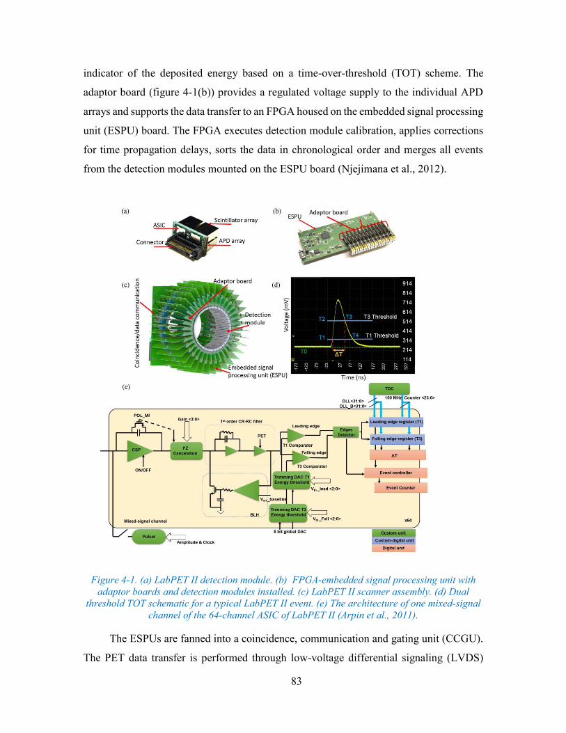
83
indicator of the deposited energy based on a time-over-threshold (TOT) scheme. The
adaptor board (figure 4-1(b)) provides a regulated voltage supply to the individual APD
arrays and supports the data transfer to an FPGA housed on the embedded signal processing
unit (ESPU) board. The FPGA executes detection module calibration, applies corrections
for time propagation delays, sorts the data in chronological order and merges all events
from the detection modules mounted on the ESPU board (Njejimana et al., 2012).
Figure 4-1. (a) LabPET II detection module. (b) FPGA-embedded signal processing unit with
adaptor boards and detection modules installed. (c) LabPET II scanner assembly. (d) Dual
threshold TOT schematic for a typical LabPET II event. (e) The architecture of one mixed-signal
channel of the 64-channel ASIC of LabPET II (Arpin et al., 2011).
The ESPUs are fanned into a coincidence, communication and gating unit (CCGU).
The PET data transfer is performed through low-voltage differential signaling (LVDS)
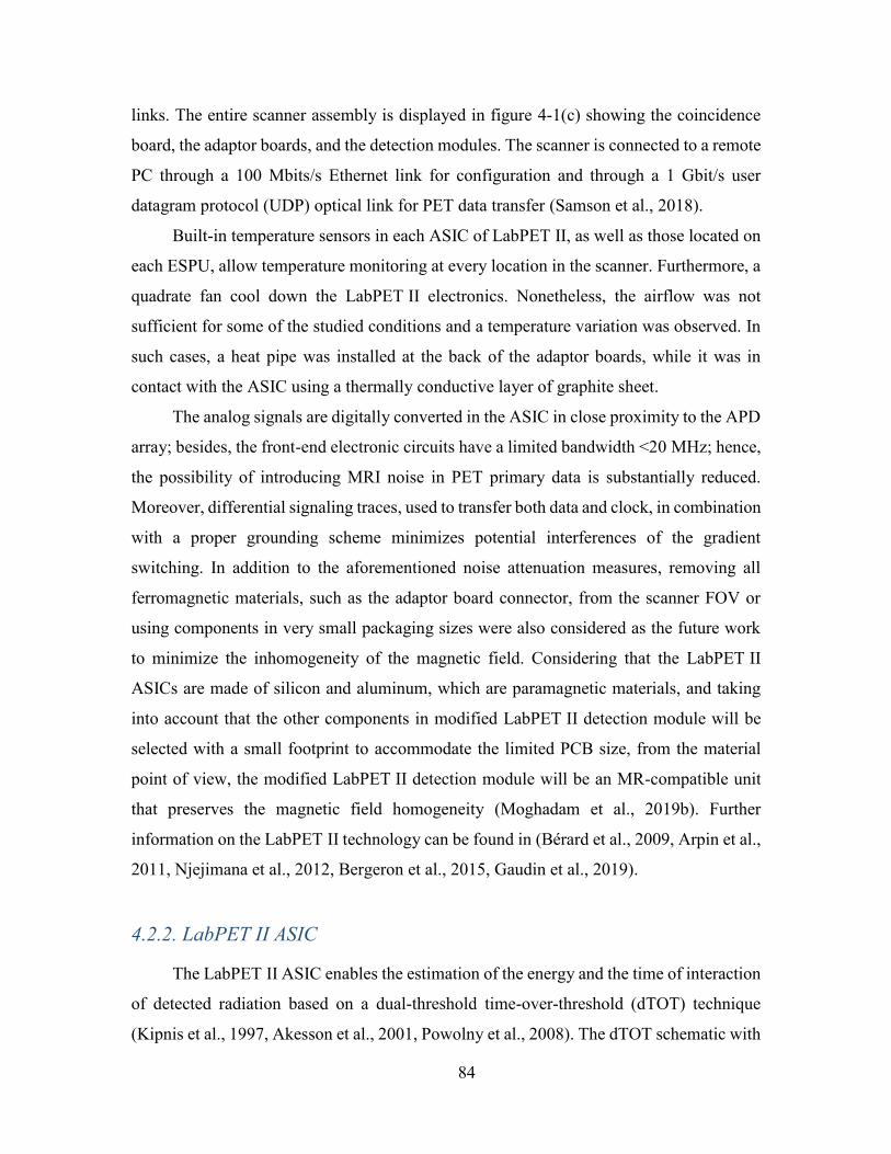
84
links. The entire scanner assembly is displayed in figure 4-1(c) showing the coincidence
board, the adaptor boards, and the detection modules. The scanner is connected to a remote
PC through a 100 Mbits/s Ethernet link for configuration and through a 1 Gbit/s user
datagram protocol (UDP) optical link for PET data transfer (Samson et al., 2018).
Built-in temperature sensors in each ASIC of LabPET II, as well as those located on
each ESPU, allow temperature monitoring at every location in the scanner. Furthermore, a
quadrate fan cool down the LabPET II electronics. Nonetheless, the airflow was not
sufficient for some of the studied conditions and a temperature variation was observed. In
such cases, a heat pipe was installed at the back of the adaptor boards, while it was in
contact with the ASIC using a thermally conductive layer of graphite sheet.
The analog signals are digitally converted in the ASIC in close proximity to the APD
array; besides, the front-end electronic circuits have a limited bandwidth <20 MHz; hence,
the possibility of introducing MRI noise in PET primary data is substantially reduced.
Moreover, differential signaling traces, used to transfer both data and clock, in combination
with a proper grounding scheme minimizes potential interferences of the gradient
switching. In addition to the aforementioned noise attenuation measures, removing all
ferromagnetic materials, such as the adaptor board connector, from the scanner FOV or
using components in very small packaging sizes were also considered as the future work
to minimize the inhomogeneity of the magnetic field. Considering that the LabPET II
ASICs are made of silicon and aluminum, which are paramagnetic materials, and taking
into account that the other components in modified LabPET II detection module will be
selected with a small footprint to accommodate the limited PCB size, from the material
point of view, the modified LabPET II detection module will be an MR-compatible unit
that preserves the magnetic field homogeneity (Moghadam et al., 2019b). Further
information on the LabPET II technology can be found in (Bérard et al., 2009, Arpin et al.,
2011, Njejimana et al., 2012, Bergeron et al., 2015, Gaudin et al., 2019).
4.2.2. LabPET II ASIC
The LabPET II ASIC enables the estimation of the energy and the time of interaction
of detected radiation based on a dual-threshold time-over-threshold (dTOT) technique
(Kipnis et al., 1997, Akesson et al., 2001, Powolny et al., 2008). The dTOT schematic with
85
two thresholds applied to a typical LabPET II signal as well as the architecture of one
mixed-signal channel in the LabPET II ASIC are shown in figure 4-1(d) and figure 4-1(e),
respectively. The signal from the APD (or from a pulser for testing purposes) at the input
of a channel of the ASIC passes through a charge sensitive pre-amplifier and a pole-zero
cancellation unit, then it is amplified via a first-order CR-RC shaper (e.g., the curve of
figure 4-1(d)). A baseline holder ensures a stable DC level at the shaper output to remove
undesirable leakage current in the APD and efficiently register the timestamps. Two
digital-to-analog converters set the desired thresholds of two comparators whose outputs
trigger a 312.5 ps delay-lock loop-based time-to-digital converter and generate timestamps
for the crossing voltage at T1 and T3, where T1 is the leading edge crossing time of the
first threshold and T3 is the falling edge crossing time of the second threshold, as shown
in figure 4-1(d) (Arpin et al., 2011). Event energy E is related non-linearly to the time-
over-threshold data (Chang et al., 2017) by an exponential monotonically increasing
function of the form ∆T = T3 - T1= a + b × ln (E), where a and b are constants to be fitted
for each individual detector pixel. The two desired thresholds for optimal timing and
energy measurements are set according to the optimized time jitter function over time as
described in (Njejimana et al., 2012). Note that both energy and time-related stamps
generated by the ASIC require correction factors applied in the ESPU to compensate for
the time walk on T1 associated with the event energy. The event is registered as digital
data in the ASIC and sent to the ESPU via a dedicated 100 Mbits/s LVDS serial link.
4.2.3. Energy And Timing Resolution Measurement Set Up
Two LabPET II detection modules (DM #1 and DM #2), described in section 4.2.1,
were placed face to face and approximately ~ 4 cm apart. The TOT energy and timing
measurements were conducted in the presence of RF coils transmitting signals with center
frequencies equivalent to the Larmor frequencies of 3 T, 7 T, and 9.4 T MRI, respectively.
Then the RF coil was replaced by the gradient coil and the measurements were repeated in
the presence of a gradient coil switching from 10 kHz to 100 kHz. The data acquisitions
were made with an 18.5 MBq 68Ge rod source positioned midway between the two
detection modules. The detection modules were calibrated without turning on any coil and
the same calibration was used for all measurements performed under the same conditions.
86
If the configuration was changed, e.g., inserting the shielding layer or temperature changes,
then the calibration was redone before starting the new series of measurements. The
experimental baseline voltages and equivalent noise values of the detection modules were
computed from the baseline histogram acquired for each pixel using a custom routine
specifically developed for the LabPET II ASIC calibration. The routine consisted of
sweeping the T1 threshold while monitoring the channel count rate (Arpin et al., 2011).
The standard deviation of the noise count-rate distribution is equivalent to the noise
presented at the charge sensitive amplifier input multiplied by the electronic gain. The
baseline voltage and the RMS noise of the analog signal for all pixels were recorded before
starting a 12-hour acquisition for coincidence time resolution measurements. Meanwhile,
the TOT energy spectra for each pixel of the arrays using a wide energy window from
250 keV to 1000 keV were stored. The same measurements were carried out for the
detection modules with RF pulses and gradient switching, independently.
4.2.4. Choice of Shielding Material
In order to eliminate EMIs, a shielding layer is required. To choose an appropriate
shielding material, two factors must be essentially considered; (i) the shielding
effectiveness (SE) and (ii) the induced eddy current. To shield the electromagnetic
interferences, a layer of conductive paint from Parker Chomerics named CHO-SHIELD®
2056 was selected and its properties were compared with copper and carbon fiber. The
composites by nature have higher electrical resistivity than metallic materials such as
copper, with a resistivity of 1.7x10⁻⁸ Ω.m. As for CHO-SHIELD® 2056 paint, the surface
resistance is 3x10⁻² Ω/m2 based on its datasheet (Parker-Chomerics, 2019). For a dry film
with a thickness of 1 mm, the electrical resistivity was calculated as 3x10⁻⁵ Ω.m, which is
a 3-order of magnitude higher than that of copper. This CHO-SHIELD® 2056 coating is a
silver/copper filled conductive acrylic paint with a cost-effective and environmentally
stable EMI shielding property.
Shielding effectiveness: The SE was measured using a modified version of the ASTM
D4923-99 standard (Vasquez et al., 2009) for the megahertz frequency range. In addition,
a modified version of IEEE Std 299.1-2013 (Ishii and Yamazaki, 2014) was used for
determining RF attenuation at kilohertz frequency range; a similar method was also used
87
for evaluating the RF attenuation of different optically transparent materials in PET/MRI
applications (Parl et al., 2017).
Eddy current measurement: Based on Faraday’s Law, the magnitude of eddy currents
depends on the alteration rate of the stimulating magnetic field. Consequently, fast imaging
sequences, such as Echo-planar imaging sequences, in which gradients are quickly
switched on and off, produce the largest and the most severe eddy current artifacts. Note
that the eddy current effects due to RF signal variations are insignificant. A simple set-up
was designed to measure eddy current induction for different materials, e.g., copper, carbon
fiber and CHO-SHIELD® 2056. To assess the eddy currents, two custom-build cylindrical
coils were made. The first coil was connected to an alternating sinisodal current source at
100 kHz and located over the tested shielding layer. The thickness of copper and
conductive paint samples was 1 mm; that is, five skin depths of copper at 100 kHz, whereas
the thickness of carbon fiber was 3 mm, based on the data presented at (Peng et al., 2014b).
The second coil was used to monitor the phase and amplitude variations of the received
signals. Note that, the 100 kHz gradient switching was selected for this specific test since
it imposes the highest amount of interaction to the detection module compared to the other
frequencies of the gradient coil. The ratio between initial voltage and secondary induced
voltage observed on an oscilloscope is a proper quantity to compare any eddy current
induction since the induced current generates an opposite field decreasing the secondary
voltage.
4.2.5. Mutual RF Interferences between the LabPET II and the RF Coil
To facilitate the measurements of RF coil interferences on the LabPET II
performance, three small hexagonal coils were designed using copper tape and capacitors
(one variable capacitor to adjust the frequency and five fixed capacitors) according to
Larmor frequency (figure 4-2 (a)). The RF coil is powered up with a signal generator
connected to an RF amplifier [Empower, Model: 1112-BBM1C3KCK]. Since the gain of
this amplifier is nonlinear, a higher power was applied to the 3 T coil than the 7 T or 9.4 T
coils. Although the power of the RF coil, a maximum of 25 W, was lower than that of a
real MRI scanner, it allowed achieving the key objectives, which included determining the
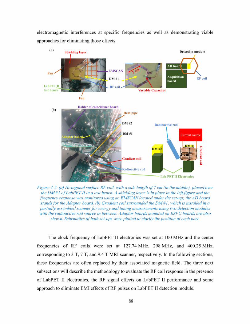
88
electromagnetic interferences at specific frequencies as well as demonstrating viable
approaches for eliminating those effects.
Figure 4-2. (a) Hexagonal surface RF coil, with a side length of 7 cm (in the middle), placed over
the DM #1 of LabPET II in a test bench. A shielding layer is in place in the left figure and the
frequency response was monitored using an EMSCAN located under the set-up; the AD board
stands for the Adaptor board. (b) Gradient coil surrounded the DM #1, which is installed in a
partially assembled scanner for energy and timing measurements using two detection modules
with the radioactive rod source in between. Adaptor boards mounted on ESPU boards are also
shown. Schematics of both set-ups were plotted to clarify the position of each part.
The clock frequency of LabPET II electronics was set at 100 MHz and the center
frequencies of RF coils were set at 127.74 MHz, 298 MHz, and 400.25 MHz,
corresponding to 3 T, 7 T, and 9.4 T MRI scanner, respectively. In the following sections,
these frequencies are often replaced by their associated magnetic field. The three next
subsections will describe the methodology to evaluate the RF coil response in the presence
of LabPET II electronics, the RF signal effects on LabPET II performance and some
approach to eliminate EMI effects of RF pulses on LabPET II detection module.
LabPET II
test bench
EMSCAN
Fan
RF coil
Shielding layer
DM #1
AD board
Acquisition
board
Detection module
RF coil
DM #2
Radioactive rod
Lab PET II Electronics
Current source
Gra
dien
t coil
Radioactive rod
DM #1
Gradient coil
Holder of coincidence board(b)
Heat pipe
Adaptor board
2 cm
DM #2
(a)
Variable Capacitor
Fan
DM #1
89
a) RF Coil Response in the Presence of LabPET II Electronics
The interaction between the RF coil signal and the LabPET II clock/signal was
measured with an EMSCAN [EMxpert: EHX-82] signal integrity analysis device
connected to a spectrum analyzer [Agilent Tech., Model: N9935A] as an RF receiver
(shown in figure 4-2(a)). The EMSCAN was placed under the test bench of the LabPET II
electronics when the 100 MHz clock was turned on, and the RF coil was powered up at the
three aforementioned frequencies, one at the time. The frequency response of the RF
emission was monitored with the EMSCAN to detect interactions between the LabPET II
clock and the different RF coil signals to ensure the preservation of the MRI signal-to-
noise ratio.
b) RF Coil Effects on LabPET II Performance
The RF coil was located parallel to the vertical side of the LabPET II DM #1 at a
distance of 1.1 mm to optimize the power transfer to the LabPET II electronics. The
1.1 mm distance was left as a gap that would be filled by a shielding layer, leaving only a
small gap (1.1 mm – 1.0254 mm = 74.6 µm) between the RF shield and the DM. The
performance of the LabPET II detection module was investigated as described in section
4.2.3 with and without turning on the RF coil at desired MRI frequencies. To obtain
consistent experimental conditions, the RF coil was in place for all the tests and the first
measurement, performed without powering up the RF coil, was used as a reference. The
configuration of the detection modules is shown in figure 4-2(b). For the RF coil
measurements, the gradient coil shown in figure 4-2(b) was removed and the RF coil was
placed vertically near DM #1. Here, the cooling system only included a quadrate fan with
a total airflow of 300 cubic feet per minute (CFM).
c) Eliminating EMI Effects of RF Coil on the LabPET II Detection Module
Shielding: To shield the RF coil from LabPET II emission and vice versa, a 1-mil
thick sheet of FR4 covered by 1-mm of CHO-SHIELD® 2056 conductive paint was placed
between the LabPET II DMs and the RF coil. The FR4 surface was initially cleaned by
acetone and IPA, which was followed by a deionized water rinsing and N2 flow drying.
Next, a uniform layer of conductive paint with 1 mm thickness was deposited over FR4.
The edges of the samples were confined using 1 mm thick microscope slides. The
90
conducting paint layer was then dried at low temperature on a 50 oC hot plate for 24 h to
avoid the formation of bubbles. The uniformity of the shielding layer was verified to be
±5%. Besides, the shielding layer was connected to the nearest LabPET II ground. The
baseline voltage, the noise level, the TOT energy resolution and the coincidence time
resolution of the two detection modules were recorded after inserting the shielding layer
between the RF coil and the DMs.
Changing the clock frequency: The LabPET II electronics clock frequency was also
changed from 100 MHz to 106 MHz for two main purposes; (i) to observe the response of
received signals from RF coil at receiver point and (ii) to verify if the RF interference from
the clock and the Double Data Rate memory type 3 (DDR3) can be eliminated from the RF
coil response, in order to preserve the SNR of the RF coils. The baseline voltage and the
noise level of the LabPET II detection modules were also recorded.
4.2.6. Mutual Interferences between the LabPET II and the Gradient Coil
a) Gradient Switching Effects on the LabPET II Performance
To simulate the effect of the gradient switching, an alternating current source
providing a maximum current of 3.5 Arms was used along with a coil to generate a slew rate
higher than 200 T/m/s at frequencies between 10 kHz to 100 kHz. The coil was made of
200 turns of 22-AWG wire wrapped around a 30 mm diameter by a 20 mm long cylinder.
DM #1 was surrounded by this gradient coil as displayed in figure 4-2(b) while DM #2 was
kept intact. To exclude temperature drifts due to the confinement of the detection module
by the gradient coil, the coil was located around DM #1 for all the measurements, including
the reference measurement without gradient switching. Since a stable temperature is
critical to eliminate the lattice heating and the APD gain variations, after initial
measurements, a heat pipe was also attached to the electronic board using a high thermal
conductive graphite sheet. Such a configuration was devised to eliminate the effects of
temperature variations because of the inserting shielding layer that impeded the normal
flow of fans.
The baseline voltage and its associated noise measurements of the LabPET II
detection modules were performed without and with the gradient switching at 10 kHz,
91
50 kHz and 100 kHz. The TOT energy resolution of each detection module and the
coincidence time resolution between the two detection modules were measured.
b) Eliminating EMI Effects of the Gradient Switching on the LabPET II Detection
Module
Shielding: Besides the temperature stabilization to remove the heat effects caused by
the gradient switching, its low-frequency emission requires a shielding layer to eliminate
the EMI effects on the LabPET II detection module. A CHO-SHIELD® 2056 conductive
paint layer deposited over a 0.18 mm thick electrical tape (TemflexTM, Model: PC695),
prepared using the same method as that of the RF shielding layer and connected to the
nearest ground of LabPET II electronics, was employed as a shielding layer using two
different configurations; (i) shielded inside the gradient coil or (ii) covered around the
LabPET II detection module. The baseline voltage, the noise level, the TOT energy
resolution and the time resolution were measured in the presence of the gradient switching.
The heat pipe cooling configuration was utilized for all these series of measurements. All
the measurements in the presence of the RF signals and gradient pulses have been repeated
three times.
4.3. Results
4.3.1. Choice of Shielding Material
Shielding effectiveness: SE comparison between all three materials is presented in
Table 4-1. Our measurement result using modified ASTM D4923-99 indicates shielding
effectiveness of 85 dB at 100 MHz for CHO-SHIELD® 2056 coating that is in a good
agreement with CHO-SHIELD® 2056 datasheet (Parker-Chomerics, 2011) and more than
80 dB for frequencies around 300 MHz and 400 MHz. All three results of SE are in the
range of the standard SE required for the PET/MRI shielding (Lamey et al., 2010). In
addition, this shielding layer provides a maximum SE of 65 dB for low frequencies down
to 10 kHz, based on our measurement using a modified version of IEEE Std 299.1-2013.
As for the carbon fiber sheet, a 3 mm thick layer covered with one layer of copper tape,
with a thickness of 0.0762 mm, provides SE of 47 dB at 81 kHz; carbon fiber layer alone
offers SE of 35 dB at low frequencies (Peng et al., 2014b). At high frequencies, however,
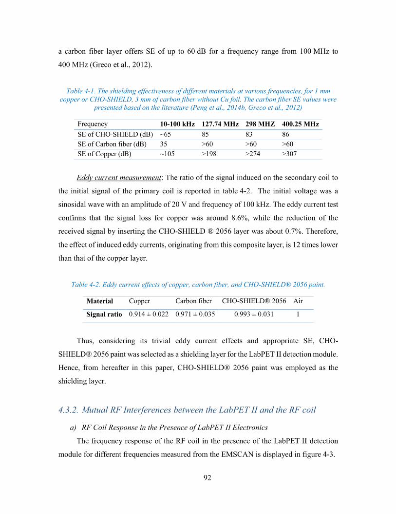
92
a carbon fiber layer offers SE of up to 60 dB for a frequency range from 100 MHz to
400 MHz (Greco et al., 2012).
Table 4-1. The shielding effectiveness of different materials at various frequencies, for 1 mm
copper or CHO-SHIELD, 3 mm of carbon fiber without Cu foil. The carbon fiber SE values were
presented based on the literature (Peng et al., 2014b, Greco et al., 2012)
Frequency 10-100 kHz 127.74 MHz 298 MHZ 400.25 MHz
SE of CHO-SHIELD (dB) ~65 85 83 86
SE of Carbon fiber (dB) 35 >60 >60 >60
SE of Copper (dB) ~105 >198 >274 >307
Eddy current measurement: The ratio of the signal induced on the secondary coil to
the initial signal of the primary coil is reported in table 4-2. The initial voltage was a
sinosidal wave with an amplitude of 20 V and frequency of 100 kHz. The eddy current test
confirms that the signal loss for copper was around 8.6%, while the reduction of the
received signal by inserting the CHO-SHIELD ® 2056 layer was about 0.7%. Therefore,
the effect of induced eddy currents, originating from this composite layer, is 12 times lower
than that of the copper layer.
Table 4-2. Eddy current effects of copper, carbon fiber, and CHO-SHIELD® 2056 paint.
Material Copper Carbon fiber CHO-SHIELD® 2056 Air
Signal ratio 0.914 ± 0.022 0.971 ± 0.035 0.993 ± 0.031 1
Thus, considering its trivial eddy current effects and appropriate SE, CHO-
SHIELD® 2056 paint was selected as a shielding layer for the LabPET II detection module.
Hence, from hereafter in this paper, CHO-SHIELD® 2056 paint was employed as the
shielding layer.
4.3.2. Mutual RF Interferences between the LabPET II and the RF coil
a) RF Coil Response in the Presence of LabPET II Electronics
The frequency response of the RF coil in the presence of the LabPET II detection
module for different frequencies measured from the EMSCAN is displayed in figure 4-3.
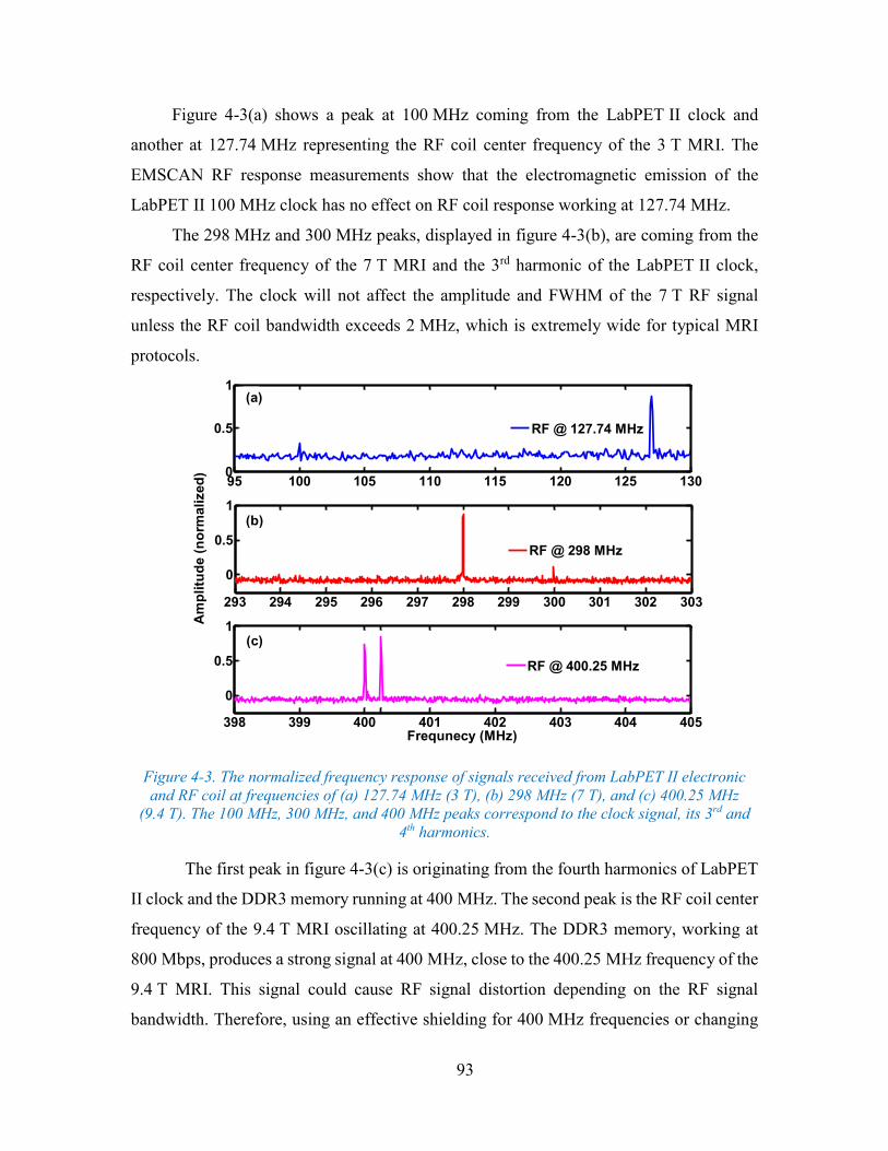
93
Figure 4-3(a) shows a peak at 100 MHz coming from the LabPET II clock and
another at 127.74 MHz representing the RF coil center frequency of the 3 T MRI. The
EMSCAN RF response measurements show that the electromagnetic emission of the
LabPET II 100 MHz clock has no effect on RF coil response working at 127.74 MHz.
The 298 MHz and 300 MHz peaks, displayed in figure 4-3(b), are coming from the
RF coil center frequency of the 7 T MRI and the 3rd harmonic of the LabPET II clock,
respectively. The clock will not affect the amplitude and FWHM of the 7 T RF signal
unless the RF coil bandwidth exceeds 2 MHz, which is extremely wide for typical MRI
protocols.
Figure 4-3. The normalized frequency response of signals received from LabPET II electronic
and RF coil at frequencies of (a) 127.74 MHz (3 T), (b) 298 MHz (7 T), and (c) 400.25 MHz
(9.4 T). The 100 MHz, 300 MHz, and 400 MHz peaks correspond to the clock signal, its 3rd and
4th harmonics.
The first peak in figure 4-3(c) is originating from the fourth harmonics of LabPET
II clock and the DDR3 memory running at 400 MHz. The second peak is the RF coil center
frequency of the 9.4 T MRI oscillating at 400.25 MHz. The DDR3 memory, working at
800 Mbps, produces a strong signal at 400 MHz, close to the 400.25 MHz frequency of the
9.4 T MRI. This signal could cause RF signal distortion depending on the RF signal
bandwidth. Therefore, using an effective shielding for 400 MHz frequencies or changing
293 294 295 296 297 298 299 300 301 302 303
0
0.5
1
398 399 400 401 402 403 404 405
0
0.5
1
Frequnecy (MHz)
Am
plitu
de (
no
rmalized
)
RF @ 298 MHz
RF @ 400.25 MHz
95 100 105 110 115 120 125 1300
0.5
1
RF @ 127.74 MHz
(b)
(c)
(a)
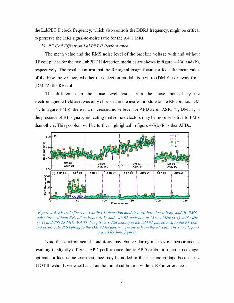
94
the LabPET II clock frequency, which also controls the DDR3 frequency, might be critical
to preserve the MRI signal-to-noise ratio for the 9.4 T MRI.
b) RF Coil Effects on LabPET II Performance
The mean value and the RMS noise level of the baseline voltage with and without
RF coil pulses for the two LabPET II detection modules are shown in figure 4-4(a) and (b),
respectively. The results confirm that the RF signal insignificantly affects the mean value
of the baseline voltage, whether the detection module is next to (DM #1) or away from
(DM #2) the RF coil.
The differences in the noise level result from the noise induced by the
electromagnetic field as it was only observed in the nearest module to the RF coil, i.e., DM
#1. In figure 4-4(b), there is an increased noise level for APD #2 on ASIC #1, DM #1, in
the presence of RF signals, indicating that some detectors may be more sensitive to EMIs
than others. This problem will be further highlighted in figure 4-7(b) for other APDs.
Figure 4-4. RF coil effects on LabPET II detection modules: (a) baseline voltage and (b) RMS
noise level without RF coil emission (0 T) and with RF emission at 127.74 MHz (3 T), 298 MHz
(7 T) and 400.25 MHz (9.4 T). The pixels 1-128 belong to the DM #1 placed next to the RF coil
and pixels 129-256 belong to the DM #2 located ~ 4 cm away from the RF coil. The same legend
is used for both figures.
Note that environmental conditions may change during a series of measurements,
resulting in slightly different APD performance due to APD calibration that is no longer
optimal. In fact, some extra variance may be added to the baseline voltage because the
dTOT thresholds were set based on the initial calibration without RF interferences.
350
400
450
500
Ba
se
lin
e (
mV
)
0 T
3 T
7 T
9.4 T
0 50 100 150 200 2500
10
20
30
40
Pixel number
RM
S N
ois
e (
mV
)
(a)
(b)
DM #1ASIC # 2
DM #2ASIC #1
APD #1 APD #2 APD #1 APD #2
DM #2ASIC #2
APD #1 APD #2 APD #1 APD #2
DM #1ASIC #1
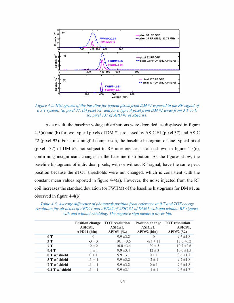
95
Figure 4-5. Histograms of the baseline for typical pixels from DM #1 exposed to the RF signal of
a 3 T system: (a) pixel 37, (b) pixel 92; and for a typical pixel from DM #2 away from 3 T coil:
(c) pixel 137 of APD #1 of ASIC #1.
As a result, the baseline voltage distributions were degraded, as displayed in figure
4-5(a) and (b) for two typical pixels of DM #1 processed by ASIC #1 (pixel 37) and ASIC
#2 (pixel 92). For a meaningful comparison, the baseline histogram of one typical pixel
(pixel 137) of DM #2, not subject to RF interferences, is also shown in figure 4-5(c),
confirming insignificant changes in the baseline distribution. As the figures show, the
baseline histograms of individual pixels, with or without RF signal, have the same peak
position because the dTOT thresholds were not changed, which is consistent with the
constant mean values reported in figure 4-4(a). However, the noise injected from the RF
coil increases the standard deviation (or FWHM) of the baseline histograms for DM #1, as
observed in figure 4-4(b)
Table 4-3. Average difference of photopeak position from reference at 0 T and TOT energy
resolution for all pixels of APD#1 and APD#2 of ASIC #1 of DM#1 with and without RF signals,
with and without shielding. The negative sign means a lower bin.
Position change
ASIC#1,
APD#1 (bin)
TOT resolution
ASIC#1,
APD#1 (%)
Position change
ASIC#1,
APD#2 (bin)
TOT resolution
ASIC#1,
APD#2 (%)
0 T 0 9.9 ±3.2 0 9.6 ±1.8
3 T -3 ± 3 10.1 ±3.5 -23 ± 11 13.6 ±6.2
7 T -2 ± 2 10.0 ±3.4 -20 ± 5 10.7 ±2.6
9.4 T -1 ± 1 9.9 ±3.4 -12 ± 3 10.0 ±1.5
0 T w/ shield 0 ± 1 9.9 ±3.1 0 ± 1 9.6 ±1.7
3 T w/ shield -1 ± 1 9.9 ±3.2 -2 ± 1 9.7 ±1.8
7 T w/ shield -1 ± 1 9.9 ±3.2 0 ± 1 9.6 ±1.8
9.4 T w/ shield -1 ± 1 9.9 ±3.1 -1 ± 1 9.6 ±1.7
0 300 440 500 600 8000
2
4
6
8
Co
un
t
10
4
0 300 428 500 600 8000
2
4
6
8
Co
un
t
10
4
pixel 92 RF OFF
pixel 92 RF ON @127.74 MHz
pixel 37 RF OFF
pixel 37 RF ON @127.74 MHz
0 300 460 600 8000
2
4
6
8
Voltage (mV)
Co
un
t
10
4
pixel 137 RF OFF
pixel 137 ON @127.74 MHz
FWHM=3.12
FWHM=20.94
FWHM=4.72
FWHM=8.06
(a)
(b)
(c)
FWHM= 2.37
FWHM= 2.61
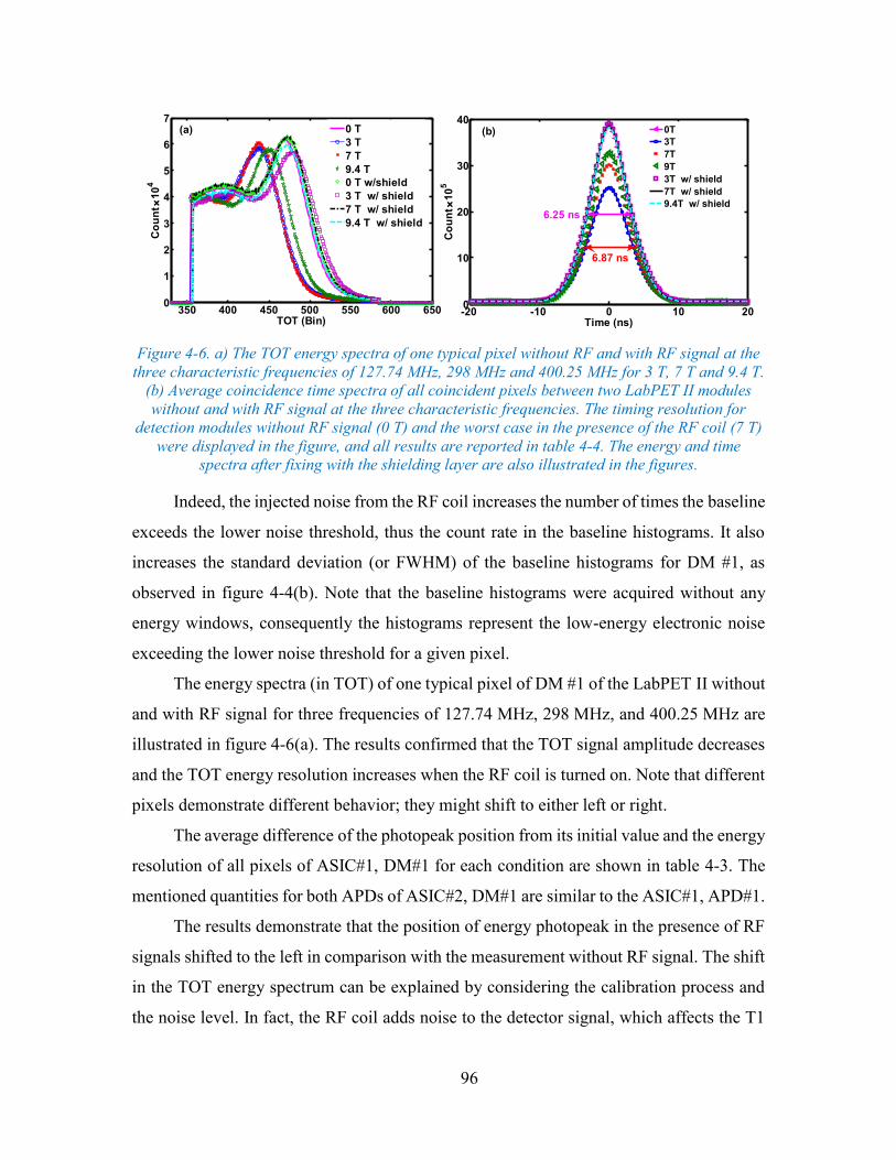
96
Figure 4-6. a) The TOT energy spectra of one typical pixel without RF and with RF signal at the
three characteristic frequencies of 127.74 MHz, 298 MHz and 400.25 MHz for 3 T, 7 T and 9.4 T.
(b) Average coincidence time spectra of all coincident pixels between two LabPET II modules
without and with RF signal at the three characteristic frequencies. The timing resolution for
detection modules without RF signal (0 T) and the worst case in the presence of the RF coil (7 T)
were displayed in the figure, and all results are reported in table 4-4. The energy and time
spectra after fixing with the shielding layer are also illustrated in the figures.
Indeed, the injected noise from the RF coil increases the number of times the baseline
exceeds the lower noise threshold, thus the count rate in the baseline histograms. It also
increases the standard deviation (or FWHM) of the baseline histograms for DM #1, as
observed in figure 4-4(b). Note that the baseline histograms were acquired without any
energy windows, consequently the histograms represent the low-energy electronic noise
exceeding the lower noise threshold for a given pixel.
The energy spectra (in TOT) of one typical pixel of DM #1 of the LabPET II without
and with RF signal for three frequencies of 127.74 MHz, 298 MHz, and 400.25 MHz are
illustrated in figure 4-6(a). The results confirmed that the TOT signal amplitude decreases
and the TOT energy resolution increases when the RF coil is turned on. Note that different
pixels demonstrate different behavior; they might shift to either left or right.
The average difference of the photopeak position from its initial value and the energy
resolution of all pixels of ASIC#1, DM#1 for each condition are shown in table 4-3. The
mentioned quantities for both APDs of ASIC#2, DM#1 are similar to the ASIC#1, APD#1.
The results demonstrate that the position of energy photopeak in the presence of RF
signals shifted to the left in comparison with the measurement without RF signal. The shift
in the TOT energy spectrum can be explained by considering the calibration process and
the noise level. In fact, the RF coil adds noise to the detector signal, which affects the T1
350 400 450 500 550 600 6500
1
2
3
4
5
6
7
TOT (Bin)
Co
un
t
10
4
0 T
3 T
7 T
9.4 T
0 T w/shield
3 T w/ shield
7 T w/ shield
9.4 T w/ shield
-20 -10 0 10 200
10
20
30
40
Time (ns)
Co
un
t
10
5
0T
3T
7T
9T
3T w/ shield
7T w/ shield
9.4T w/ shield
(a) (b)
6.87 ns
6.25 ns
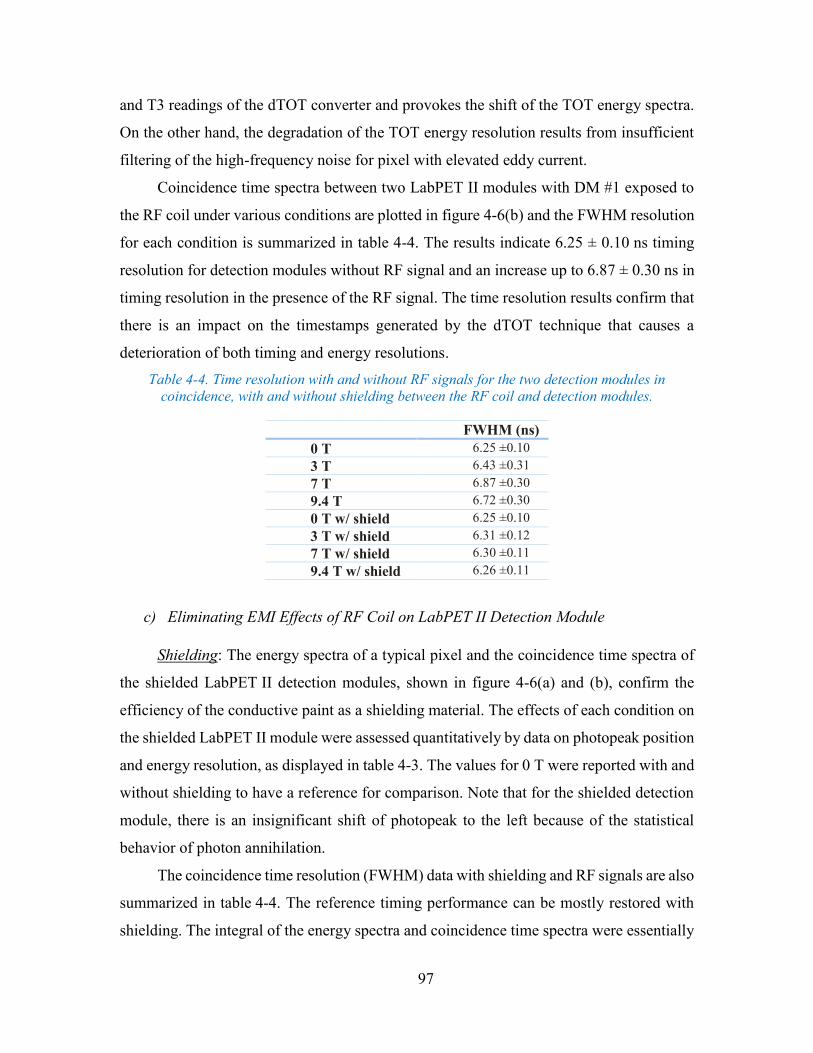
97
and T3 readings of the dTOT converter and provokes the shift of the TOT energy spectra.
On the other hand, the degradation of the TOT energy resolution results from insufficient
filtering of the high-frequency noise for pixel with elevated eddy current.
Coincidence time spectra between two LabPET II modules with DM #1 exposed to
the RF coil under various conditions are plotted in figure 4-6(b) and the FWHM resolution
for each condition is summarized in table 4-4. The results indicate 6.25 ± 0.10 ns timing
resolution for detection modules without RF signal and an increase up to 6.87 ± 0.30 ns in
timing resolution in the presence of the RF signal. The time resolution results confirm that
there is an impact on the timestamps generated by the dTOT technique that causes a
deterioration of both timing and energy resolutions.
Table 4-4. Time resolution with and without RF signals for the two detection modules in
coincidence, with and without shielding between the RF coil and detection modules.
FWHM (ns)
0 T 6.25 ±0.10
3 T 6.43 ±0.31
7 T 6.87 ±0.30
9.4 T 6.72 ±0.30
0 T w/ shield 6.25 ±0.10
3 T w/ shield 6.31 ±0.12
7 T w/ shield 6.30 ±0.11
9.4 T w/ shield 6.26 ±0.11
c) Eliminating EMI Effects of RF Coil on LabPET II Detection Module
Shielding: The energy spectra of a typical pixel and the coincidence time spectra of
the shielded LabPET II detection modules, shown in figure 4-6(a) and (b), confirm the
efficiency of the conductive paint as a shielding material. The effects of each condition on
the shielded LabPET II module were assessed quantitatively by data on photopeak position
and energy resolution, as displayed in table 4-3. The values for 0 T were reported with and
without shielding to have a reference for comparison. Note that for the shielded detection
module, there is an insignificant shift of photopeak to the left because of the statistical
behavior of photon annihilation.
The coincidence time resolution (FWHM) data with shielding and RF signals are also
summarized in table 4-4. The reference timing performance can be mostly restored with
shielding. The integral of the energy spectra and coincidence time spectra were essentially
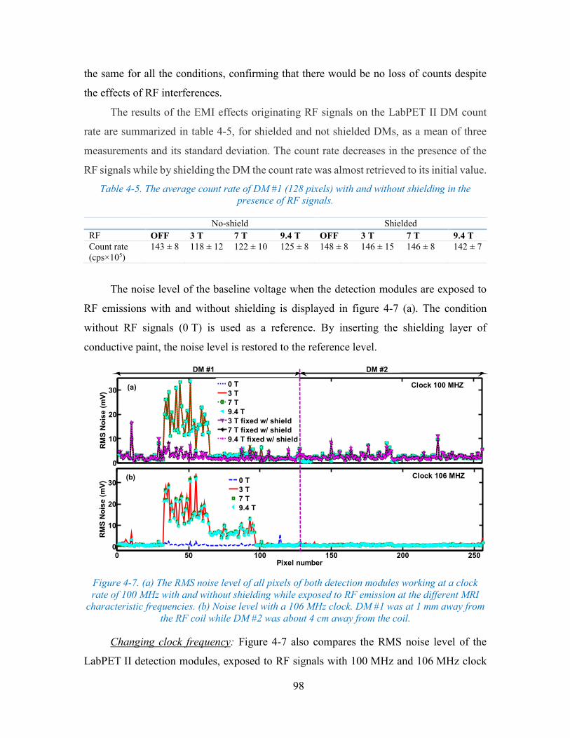
98
the same for all the conditions, confirming that there would be no loss of counts despite
the effects of RF interferences.
The results of the EMI effects originating RF signals on the LabPET II DM count
rate are summarized in table 4-5, for shielded and not shielded DMs, as a mean of three
measurements and its standard deviation. The count rate decreases in the presence of the
RF signals while by shielding the DM the count rate was almost retrieved to its initial value.
Table 4-5. The average count rate of DM #1 (128 pixels) with and without shielding in the
presence of RF signals.
No-shield Shielded
RF OFF 3 T 7 T 9.4 T OFF 3 T 7 T 9.4 T
Count rate
(cps×105)
143 ± 8 118 ± 12 122 ± 10 125 ± 8 148 ± 8 146 ± 15 146 ± 8 142 ± 7
The noise level of the baseline voltage when the detection modules are exposed to
RF emissions with and without shielding is displayed in figure 4-7 (a). The condition
without RF signals (0 T) is used as a reference. By inserting the shielding layer of
conductive paint, the noise level is restored to the reference level.
Figure 4-7. (a) The RMS noise level of all pixels of both detection modules working at a clock
rate of 100 MHz with and without shielding while exposed to RF emission at the different MRI
characteristic frequencies. (b) Noise level with a 106 MHz clock. DM #1 was at 1 mm away from
the RF coil while DM #2 was about 4 cm away from the coil.
Changing clock frequency: Figure 4-7 also compares the RMS noise level of the
LabPET II detection modules, exposed to RF signals with 100 MHz and 106 MHz clock
0
10
20
30
RM
S N
ois
e (
mV
)
0 T
3 T
7 T
9.4 T
3 T fixed w/ shield
7 T fixed w/ shield
9.4 T fixed w/ shield
0 50 100 150 200 2500
10
20
30
Pixel number
RM
S N
ois
e (
mV
)
0 T
3 T
7 T
9.4 T
(b)
(a)
DM #1 DM #2
Clock 100 MHZ
Clock 106 MHZ
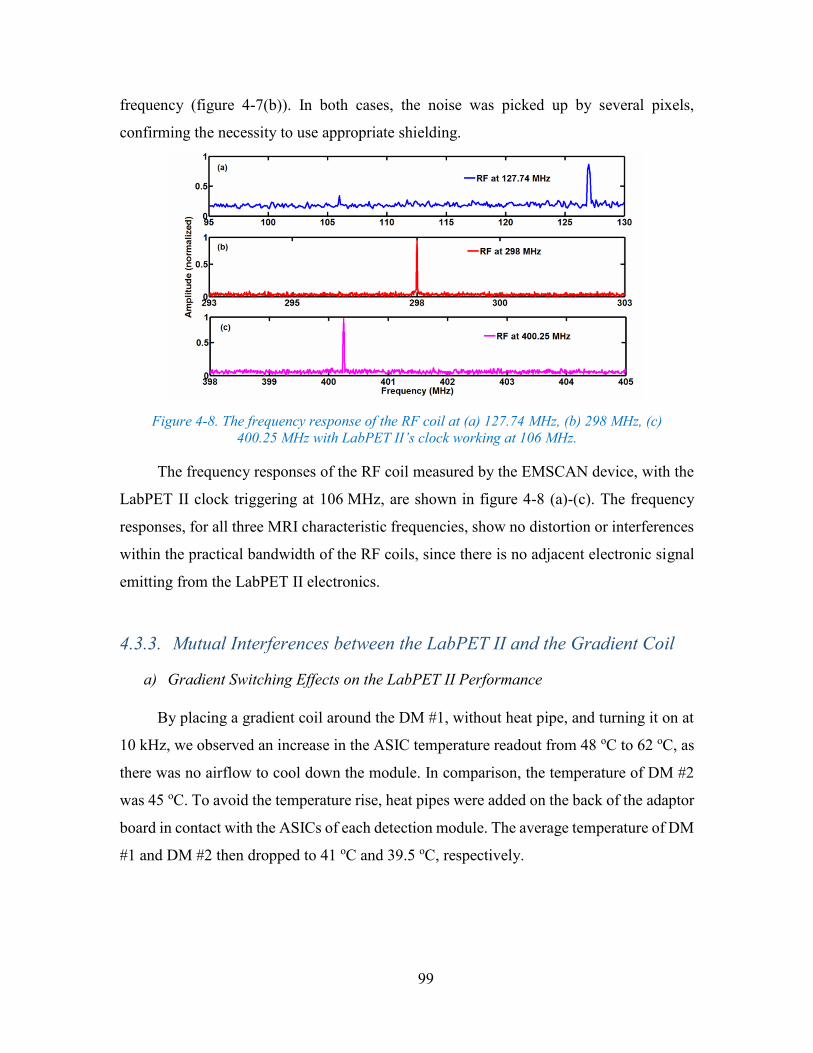
99
frequency (figure 4-7(b)). In both cases, the noise was picked up by several pixels,
confirming the necessity to use appropriate shielding.
Figure 4-8. The frequency response of the RF coil at (a) 127.74 MHz, (b) 298 MHz, (c)
400.25 MHz with LabPET II’s clock working at 106 MHz.
The frequency responses of the RF coil measured by the EMSCAN device, with the
LabPET II clock triggering at 106 MHz, are shown in figure 4-8 (a)-(c). The frequency
responses, for all three MRI characteristic frequencies, show no distortion or interferences
within the practical bandwidth of the RF coils, since there is no adjacent electronic signal
emitting from the LabPET II electronics.
4.3.3. Mutual Interferences between the LabPET II and the Gradient Coil
a) Gradient Switching Effects on the LabPET II Performance
By placing a gradient coil around the DM #1, without heat pipe, and turning it on at
10 kHz, we observed an increase in the ASIC temperature readout from 48 oC to 62 oC, as
there was no airflow to cool down the module. In comparison, the temperature of DM #2
was 45 oC. To avoid the temperature rise, heat pipes were added on the back of the adaptor
board in contact with the ASICs of each detection module. The average temperature of DM
#1 and DM #2 then dropped to 41 oC and 39.5 oC, respectively.
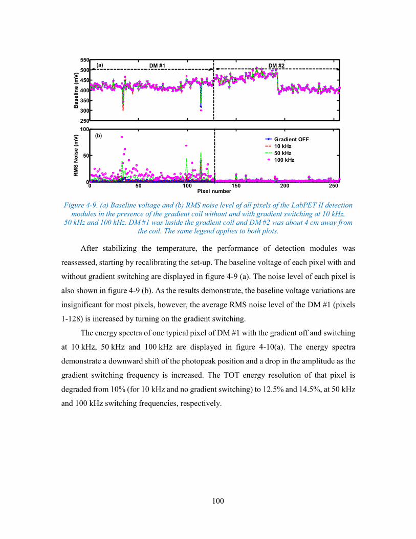
100
Figure 4-9. (a) Baseline voltage and (b) RMS noise level of all pixels of the LabPET II detection
modules in the presence of the gradient coil without and with gradient switching at 10 kHz,
50 kHz and 100 kHz. DM #1 was inside the gradient coil and DM #2 was about 4 cm away from
the coil. The same legend applies to both plots.
After stabilizing the temperature, the performance of detection modules was
reassessed, starting by recalibrating the set-up. The baseline voltage of each pixel with and
without gradient switching are displayed in figure 4-9 (a). The noise level of each pixel is
also shown in figure 4-9 (b). As the results demonstrate, the baseline voltage variations are
insignificant for most pixels, however, the average RMS noise level of the DM #1 (pixels
1-128) is increased by turning on the gradient switching.
The energy spectra of one typical pixel of DM #1 with the gradient off and switching
at 10 kHz, 50 kHz and 100 kHz are displayed in figure 4-10(a). The energy spectra
demonstrate a downward shift of the photopeak position and a drop in the amplitude as the
gradient switching frequency is increased. The TOT energy resolution of that pixel is
degraded from 10% (for 10 kHz and no gradient switching) to 12.5% and 14.5%, at 50 kHz
and 100 kHz switching frequencies, respectively.
250
300
350
400
450
500
550
Ba
se
lin
e (
mV
)
0 50 100 150 200 2500
50
100
Pixel number
RM
S N
ois
e (
mV
)
Gradient OFF
10 kHz
50 kHz
100 kHz
(a)
(b)
DM #1 DM #2
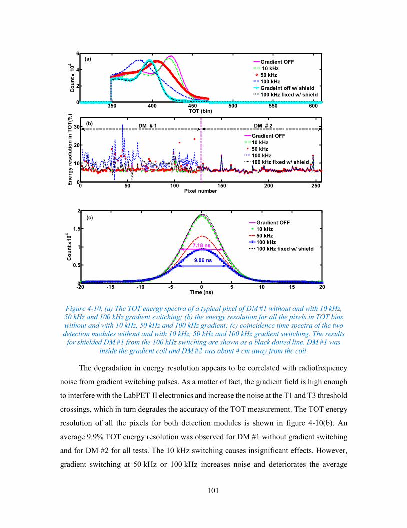
101
Figure 4-10. (a) The TOT energy spectra of a typical pixel of DM #1 without and with 10 kHz,
50 kHz and 100 kHz gradient switching; (b) the energy resolution for all the pixels in TOT bins
without and with 10 kHz, 50 kHz and 100 kHz gradient; (c) coincidence time spectra of the two
detection modules without and with 10 kHz, 50 kHz and 100 kHz gradient switching. The results
for shielded DM #1 from the 100 kHz switching are shown as a black dotted line. DM #1 was
inside the gradient coil and DM #2 was about 4 cm away from the coil.
The degradation in energy resolution appears to be correlated with radiofrequency
noise from gradient switching pulses. As a matter of fact, the gradient field is high enough
to interfere with the LabPET II electronics and increase the noise at the T1 and T3 threshold
crossings, which in turn degrades the accuracy of the TOT measurement. The TOT energy
resolution of all the pixels for both detection modules is shown in figure 4-10(b). An
average 9.9% TOT energy resolution was observed for DM #1 without gradient switching
and for DM #2 for all tests. The 10 kHz switching causes insignificant effects. However,
gradient switching at 50 kHz or 100 kHz increases noise and deteriorates the average
350 400 450 500 550 6000
2
4
6
TOT (bin)
Co
un
t
10
4
Gradient OFF
10 kHz
50 kHz
100 kHz
Gradeint off w/ shield
100 kHz fixed w/ shield
0 50 100 150 200 2500
10
20
30
Pixel number
En
erg
y r
es
olu
tio
n i
n T
OT
(%)
Gradient OFF
10 kHz
50 kHz
100 kHz
100 kHz fixed w/ shield
(a)
DM # 2DM # 1(b)
-20 -15 -10 -5 0 5 10 15 200
0.5
1
1.5
2
Time (ns)
Co
un
t
10
4
Gradient OFF
10 kHz
50 kHz
100 kHz
100 kHz fixed w/ shield
(c)
7.18 ns
9.06 ns
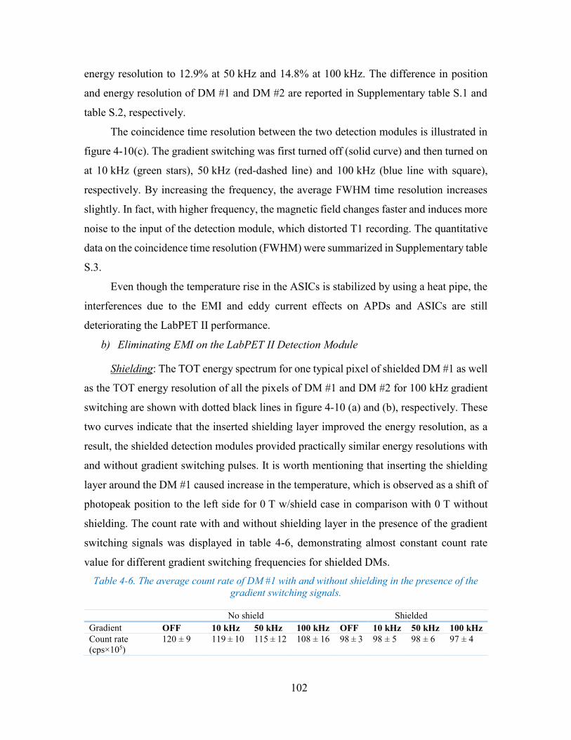
102
energy resolution to 12.9% at 50 kHz and 14.8% at 100 kHz. The difference in position
and energy resolution of DM #1 and DM #2 are reported in Supplementary table S.1 and
table S.2, respectively.
The coincidence time resolution between the two detection modules is illustrated in
figure 4-10(c). The gradient switching was first turned off (solid curve) and then turned on
at 10 kHz (green stars), 50 kHz (red-dashed line) and 100 kHz (blue line with square),
respectively. By increasing the frequency, the average FWHM time resolution increases
slightly. In fact, with higher frequency, the magnetic field changes faster and induces more
noise to the input of the detection module, which distorted T1 recording. The quantitative
data on the coincidence time resolution (FWHM) were summarized in Supplementary table
S.3.
Even though the temperature rise in the ASICs is stabilized by using a heat pipe, the
interferences due to the EMI and eddy current effects on APDs and ASICs are still
deteriorating the LabPET II performance.
b) Eliminating EMI on the LabPET II Detection Module
Shielding: The TOT energy spectrum for one typical pixel of shielded DM #1 as well
as the TOT energy resolution of all the pixels of DM #1 and DM #2 for 100 kHz gradient
switching are shown with dotted black lines in figure 4-10 (a) and (b), respectively. These
two curves indicate that the inserted shielding layer improved the energy resolution, as a
result, the shielded detection modules provided practically similar energy resolutions with
and without gradient switching pulses. It is worth mentioning that inserting the shielding
layer around the DM #1 caused increase in the temperature, which is observed as a shift of
photopeak position to the left side for 0 T w/shield case in comparison with 0 T without
shielding. The count rate with and without shielding layer in the presence of the gradient
switching signals was displayed in table 4-6, demonstrating almost constant count rate
value for different gradient switching frequencies for shielded DMs.
Table 4-6. The average count rate of DM #1 with and without shielding in the presence of the
gradient switching signals.
No shield Shielded
Gradient OFF 10 kHz 50 kHz 100 kHz OFF 10 kHz 50 kHz 100 kHz
Count rate
(cps×105)
120 ± 9 119 ± 10 115 ± 12 108 ± 16 98 ± 3 98 ± 5 98 ± 6 97 ± 4
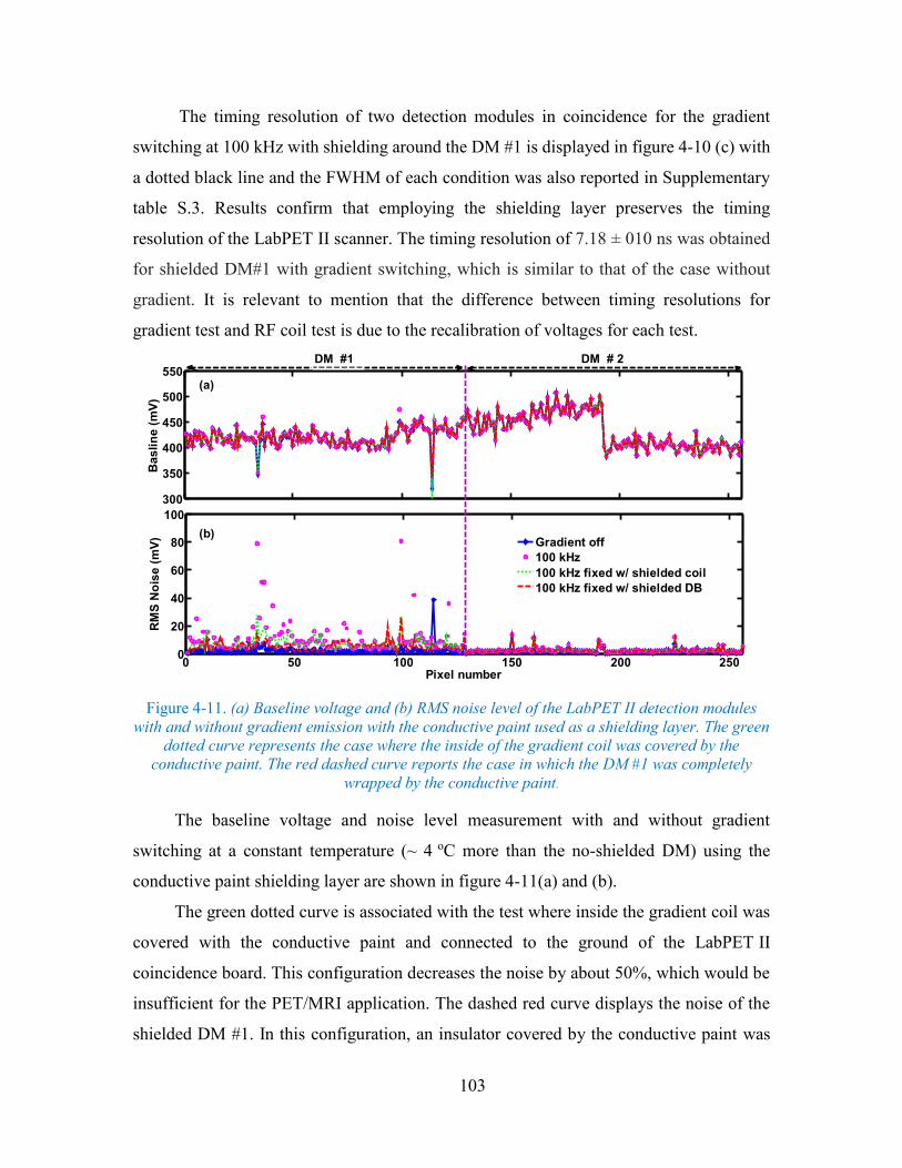
103
The timing resolution of two detection modules in coincidence for the gradient
switching at 100 kHz with shielding around the DM #1 is displayed in figure 4-10 (c) with
a dotted black line and the FWHM of each condition was also reported in Supplementary
table S.3. Results confirm that employing the shielding layer preserves the timing
resolution of the LabPET II scanner. The timing resolution of 7.18 ± 010 ns was obtained
for shielded DM#1 with gradient switching, which is similar to that of the case without
gradient. It is relevant to mention that the difference between timing resolutions for
gradient test and RF coil test is due to the recalibration of voltages for each test.
Figure 4-11. (a) Baseline voltage and (b) RMS noise level of the LabPET II detection modules
with and without gradient emission with the conductive paint used as a shielding layer. The green
dotted curve represents the case where the inside of the gradient coil was covered by the
conductive paint. The red dashed curve reports the case in which the DM #1 was completely
wrapped by the conductive paint.
The baseline voltage and noise level measurement with and without gradient
switching at a constant temperature (~ 4 oC more than the no-shielded DM) using the
conductive paint shielding layer are shown in figure 4-11(a) and (b).
The green dotted curve is associated with the test where inside the gradient coil was
covered with the conductive paint and connected to the ground of the LabPET II
coincidence board. This configuration decreases the noise by about 50%, which would be
insufficient for the PET/MRI application. The dashed red curve displays the noise of the
shielded DM #1. In this configuration, an insulator covered by the conductive paint was
0 50 100 150 200 2500
20
40
60
80
100
Pixel number
RM
S N
ois
e (
mV
)
300
350
400
450
500
550
Ba
sli
ne
(m
V)
Gradient off
100 kHz
100 kHz fixed w/ shielded coil
100 kHz fixed w/ shielded DB
(b)
(a)
DM #1 DM # 2
104
wrapped around the entire detection module. This arrangement reduces the noise close to
the initial noise value. However the temperature of the enclosed detection module increases
by 4 oC. Therefore, it is plausible to consider that the previous configuration was unable to
prevent gradient emission from reaching the APDs and ASIC inputs from ASICs and
crystal sides, as the EMIs were not entirely compensated. The results endorse the fact that
unwanted EMI effects, from low-frequency gradient switching, can be eliminated by this
new shielding composite.
Similar coincidence time resolution is achieved with and without gradient switching
using a proper shielding configuration. It confirms that the parameter related to the timing
resolution (T1) obtained through the TOT technique was not affected for shielded DM.
Consequently, variations in the noise level and energy resolution in these situations can be
attributed to the temperature rise resulting from shielding confinement.
4.4. Discussion
The MR-compatibility of the LabPET II detection modules through testing their
performance in the presence of RF coils excited at frequencies corresponding to 3 T, 7 T,
and 9.4 T magnetic field strength, as well as the switching gradient from 10 kHz to
100 kHz, was examined. The results demonstrate that the MRI coils cause insignificant
interferences on the LabPET II detection module when judiciously applying EMI shielding.
Conversely, our measurements also indicate that the RF response is immune to EM
emission from the LabPET II module. A more comprehensive study inside real MRI
scanners, however, should be carried out with a modified version of the LabPET II front-
end electronics and the shielded coincidence board to further confirm these results.
The EMI measurement methods could be applicable to other ASIC based systems
such as the PETsys TOFPET 1&2 ASICs (Schug et al., 2019), the Hamamatsu modules
with their 18-channel ToT ASICs (Goertzen and Van Elburg, 2019), or the Philips digital
photon counter (DPC) based detectors (Brunner et al., 2016). The same shielding method
could also be used to enhance their EMI/EMC compatibility with an MRI scanner if
needed. In addition, the same evaluation method could be applied to assess other shielding
layers for their MR-compatibility in terms of eddy current induction.
105
In all measurements, it was important to determine whether the observed changes
were due to genuine electromagnetic interferences or indirect side effects resulting from,
for instance, temperature variations. Due to the confinement of the detector modules in the
vicinity of the RF and gradient coils, there were temperature increases in many situations.
For instance, the gradient coil completely surrounding the detector module induced a
temperature increase of ~10 °C, on the other hand, the fast switching signal in the coil wires
also generated I-R losses that increased the detection module temperature of another ~4 °C.
Increasing the APD temperature induces a drop of the APD multiplication gain that can be
compensated by a bias correction of ~2 V/°C, but it also increases the APDs leakage current
and noise. The baseline holder embedded in the ASIC can sink up to 3 µA of leakage
current, while the individual APD leakage current is typically in the few nA range.
Therefore, the effects of small temperature increment due to the detection module
confinement or RF and gradient interferences were easily compensated by the baseline
holder and the baseline voltage level generally remained unchanged regardless of
temperature variations. However, a ~15 °C increment in temperature could not always be
compensated by the baseline holder. In fact, our first measurements without temperature
stabilization showed some faulty pixels that could not be biased within the APD operating
range. Considering typical APD characteristics, it may occur that increasing the
temperature generates a dark current beyond the baseline holder limit saturating the front-
end electronics and causing a preamplifier failure. Besides, if several pixels show high dark
current, then the high voltage (HV) controller embedded in the ASIC is unable to provide
the appropriate bias voltage due to the high total leakage current drained by the multiple
acquisition channels of a detection array. In the case where the shielding and the heat pipe
were present, as the heat was transferred efficiently, the dark current did not exceed the
limit of the baseline holder and the temperature effects were not tangible.
The shift of energy spectrum, induced by the RF coil signals, was originally
attributed to the frequency interferences and the temperature increments. Nevertheless, our
studies confirmed that this effect is highly related to the electromagnetic interferences of
the RF coil with LabPET II electronics. Although the built-in shaper filter in the ASIC was
designed to attenuate frequency up to 20 MHz, the noise injection was observed in the
LabPET II electronics due to the inability of filters to block the high-frequency noise for
106
pixels with elevated leakage current. Consequently, by placing an RF coil close to the
detection module, the noise injected from the RF coil interacted with the ASIC signals and
changed the amplitude and the shape of the input signals. Accordingly, the initial
calibration was no longer valid for some of the arrays and it caused a shift in the energy
spectrum of each pixel of that specific array.
For gradient switching tests, as the temperature was stabilized by means of a heat
pipe, the shifts of photopeak position in the TOT energy spectra were induced by the
gradient pulses and were not related to temperature variations. Hence, the EMIs had to be
compensated by a shielding layer.
Considering the clock harmonics and DDR3 peak signal at 400 MHz, near the RF
signal of 9.4 T MRI, the LabPET II electronic clock can be changed from 100 MHz to
106 MHz without detrimental effects, in order to eliminate any possible interferences of
LabPET II signal with RF signal and preserve its SNR for different magnetic fields.
Based on the obtained results, an appropriate shielding configuration makes it
possible to fabricate an MR-compatible PET scanner based on LabPET II detection
modules. In addition, by changing the shielding material from a metallic one to a
conductive paint layer, the gradient EMIs were eliminated along with the possibility to
decrease the gradient-induced eddy current effects. Nonetheless, the conductive paint layer
showed excellent performance for shielding the low-frequency EMI and reducing the eddy
currents. The proposed conductive paint has similar conductivity values as carbon fiber
shielding for high frequencies (Peng et al., 2014b) while offering more flexibility, to cover
the required surface, and lighter weight. Besides, this composite has shielding effectiveness
of 65 dB for low frequencies down to 10 kHz to reduce unwanted low frequency switching
interactions from gradients, whereas it is impossible to eliminate the interferences from
gradient with carbon fiber. Thus, PET/MRI scanner based on carbon fiber shielding
necessitates an additional layer of copper to eliminate the gradient effects, which in turn
cause eddy current induction and chemical shift errors (Peng et al., 2014b). By applying a
1 mm layer of the conductive paint for shielding both RF and gradient switching EMI, the
LabPET II detection module experiences less eddy current induction and, consequently, it
provides the possibility to acquire images with fast gradient switching sequences.
Considering these criteria, shielded LabPET II detection modules would appear as suitable
107
candidates for an MR-compatible PET-insert with simultaneous PET/MRI imaging
capability.
In this report, we focused on identifying possible interferences from RF coil and
gradient switching of an MRI scanner and provided an approach to reduce the effects of
those undesirable interactions for developing a simultaneous PET/MRI scanner based on
the LabPET II detection module. In future work, a ring of the shielded LabPET II modules
will be inserted in a clinical 3 T MRI to examine the effects of the PET-insert on MRI
performance and to investigate the required techniques for eliminating any disturbing
issues to design a true simultaneous PET/MRI for the human brain.
4.5. Conclusion
The results confirm the feasibility of using shielded LabPET II detection modules in
the presence of EMIs at the Larmor frequency of different MRI scanners. After some
material modifications to remove ferromagnetic components, it would be a viable
candidate for designing a simultaneous PET/MRI scanner with a submillimeter spatial
resolution of PET images. By using the CHO-SHIELD® 2056 paint as an EMI shielding
layer, not only the effects of frequency interferences from both the RF coil and gradient
switching were compensated, but the eddy currents were also reduced owing to the lower
conductivity of the shielding material. Furthermore, by stabilizing the temperature using
heat pipes, the undesirable effects of APD gain variations due to temperature changes were
eliminated. One key advantage of the LabPET II technology is that analog signals are
digitized directly in the ASICs, very close to the APDs, making them much less prone to
interferences. Further work will be conducted to verify the performance of a modified
version of the LabPET II detection module inside an MRI to confirm our findings.
Acknowledgments
The authors would like to thank Christian Thibaudeau, Haithem Bouziri and Caroline
Paulin for their help. This work was supported by Le Fonds de Recherche du Québec –
Nature et Technologies (FRQNT) and the Natural Sciences and Engineering Research
Council of Canada (NSERC). The authors would also like to acknowledge financial aid
108
from the Quebec Bio-Imaging Network (QBIN) and to thank Matrix Technology Ltd. for
supplying the CHO-SHIELD® 2056 sample.
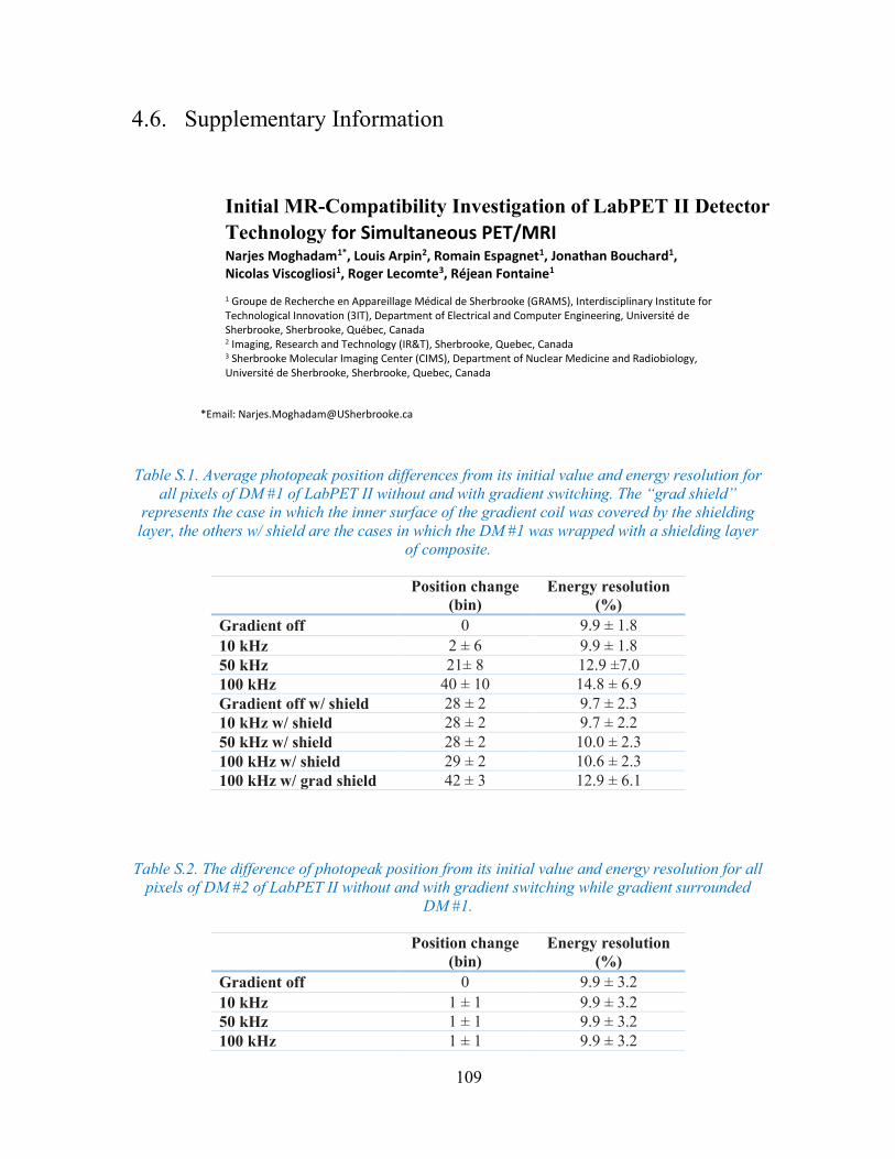
109
4.6. Supplementary Information
Initial MR-Compatibility Investigation of LabPET II Detector
Technology for Simultaneous PET/MRI Narjes Moghadam1*, Louis Arpin2, Romain Espagnet1, Jonathan Bouchard1, Nicolas Viscogliosi1, Roger Lecomte3, Réjean Fontaine1
1 Groupe de Recherche en Appareillage Médical de Sherbrooke (GRAMS), Interdisciplinary Institute for Technological Innovation (3IT), Department of Electrical and Computer Engineering, Université de Sherbrooke, Sherbrooke, Québec, Canada 2 Imaging, Research and Technology (IR&T), Sherbrooke, Quebec, Canada 3 Sherbrooke Molecular Imaging Center (CIMS), Department of Nuclear Medicine and Radiobiology, Université de Sherbrooke, Sherbrooke, Quebec, Canada
*Email: [email protected]
Table S.1. Average photopeak position differences from its initial value and energy resolution for
all pixels of DM #1 of LabPET II without and with gradient switching. The “grad shield”
represents the case in which the inner surface of the gradient coil was covered by the shielding
layer, the others w/ shield are the cases in which the DM #1 was wrapped with a shielding layer
of composite.
Position change
(bin)
Energy resolution
(%)
Gradient off 0 9.9 ± 1.8
10 kHz 2 ± 6 9.9 ± 1.8
50 kHz 21± 8 12.9 ±7.0
100 kHz 40 ± 10 14.8 ± 6.9
Gradient off w/ shield 28 ± 2 9.7 ± 2.3
10 kHz w/ shield 28 ± 2 9.7 ± 2.2
50 kHz w/ shield 28 ± 2 10.0 ± 2.3
100 kHz w/ shield 29 ± 2 10.6 ± 2.3
100 kHz w/ grad shield 42 ± 3 12.9 ± 6.1
Table S.2. The difference of photopeak position from its initial value and energy resolution for all
pixels of DM #2 of LabPET II without and with gradient switching while gradient surrounded
DM #1.
Position change
(bin)
Energy resolution
(%)
Gradient off 0 9.9 ± 3.2
10 kHz 1 ± 1 9.9 ± 3.2
50 kHz 1 ± 1 9.9 ± 3.2
100 kHz 1 ± 1 9.9 ± 3.2
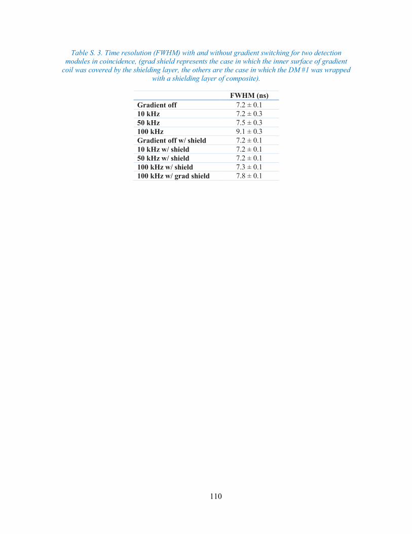
110
Table S. 3. Time resolution (FWHM) with and without gradient switching for two detection
modules in coincidence, (grad shield represents the case in which the inner surface of gradient
coil was covered by the shielding layer, the others are the case in which the DM #1 was wrapped
with a shielding layer of composite).
FWHM (ns)
Gradient off 7.2 ± 0.1
10 kHz 7.2 ± 0.3
50 kHz 7.5 ± 0.3
100 kHz 9.1 ± 0.3
Gradient off w/ shield 7.2 ± 0.1
10 kHz w/ shield 7.2 ± 0.1
50 kHz w/ shield 7.2 ± 0.1
100 kHz w/ shield 7.3 ± 0.1
100 kHz w/ grad shield 7.8 ± 0.1

111
112
CHAPTER 5
INTERPOSER: PERFORMANCE AND
MODIFICATION
Avant-propos
Auteurs et Affiliation:
Narjes Moghadam: étudiante au doctorat, Institut interdisciplinaire
d’innovation technologique - 3IT, Université de Sherbrooke, Faculté de génie,
Département de génie électrique et de génie informatique.
Jonathan Bouchard: étudiant au doctorat, Institut interdisciplinaire d’innovation
technologique - 3IT, Université de Sherbrooke, Faculté de génie, Département
de génie électrique et de génie informatique
Romain Espagnet : post-doctorant, Institut interdisciplinaire d’innovation
technologique - 3IT, Université de Sherbrooke, Faculté de génie, Département
de génie électrique et de génie informatique.
Roger Lecomte: professeur, Université de Sherbrooke, Département de
médecine nucléaire et de radiobiologie
Réjean Fontaine: professeur, Institut interdisciplinaire d’innovation
technologique - 3IT, Université de Sherbrooke, Faculté de génie, Département
de génie électrique et de génie informatique.
Date d’acceptation : xxx
État de l’acceptation : Submitted
Revue : Nuclear Inst. and Methods in Physics Research, A
Titre français : Étude de la compatibilité à l'IRM d'une nouvelle électronique frontale
LabPET II à bas profil dédiée à la tomographie d'émission par positrons
Contribution au document :
Dans ce troisième article nous examinons les effets de l'IRM sur une version modifiée
du module de détection de LabPET II appelée interposeur. Les valeurs de référence, le
bruit RMS et la résolution en énergie ont été acquis pour démontrer les performance de
cette nouvelle version du module LabPET II. L'interposeur a été conçu pour être
compatible avec l'IRM. Afin d'éliminer des effets indésirables de signaux IRM sur la
version interposeur, une couche de blindage composite a été utilisée pour améliorer les
113
performances. Nos résultats confirment que, même si la nouvelle conception offre une
amélioration des performances du module de détection, le blindage reste nécessaire.
Résumé en français:
Le module de détection LabPET II est un candidat viable pour être intégré dans un
scanner d'imagerie par résonance magnétique. Cependant, la faisabilité d'une telle bi-
modalité est limitée par la grande taille radiale du module de détection ainsi que par les
composants contenant des matériaux ferromagnétiques. Dans cet article, nous étudions une
nouvelle électronique frontale basée sur l’architecture LabPET II, appelée «détecteur
interposeur». Les performances du détecteur interposeur en présence de signaux RF et
d'impulsions d’un bobine à gradient y sont examinées. Les résultats montrent que les
impulsions dans les plages du kilohertz et du mégahertz entraînent une détérioration de la
résolution en énergie (TOT) (~17%) et du niveau de bruit de base (2 fois). En insérant une
couche de blindage composite autour du détecteur d’interposeur, les distorsions ont été
éliminées.
Mots clés: Blindage électromagnétique, Interférences en radio fréquences, scanner TEP /
IRM, Électronique ultra-haute densité
Contribution of this document to the thesis (English):
In the third article, the effects of MRI on a modified version of the LabPET II
detection module called interposer detector were examined. The baseline, RMS noise, and
energy resolution were acquired to demonstrate the performance of the new module. The
interposer was designed with the aim to be MRI compatible, but since the results
demonstrate an interaction of the MRI signals with the interposer, a composite shielding
layer was utilized to improve the interposer performance. Our results confirm that even
though the new design offers improvement in the detection module performance, it still
required a shielding method to meet the PET/MRI prerequisite.
*The context may vary from the published paper.
114
MRI-Compatibility Study of a Low-Profile
Positron Emission Tomography Front End
with Submillimeter Resolution
Abstract— The LabPET II detection module is a viable candidate to create an MRI
compatible PET-insert. However, the feasibility of such an insert is restricted by the large
radial size of the detection module as well as by the electronic components containing
ferromagnetic materials. In this paper, a new low-profile front-end electronic module based
on the LabPET II architecture, called “interposer detector,” is investigated. The
performance of the interposer detector in the presence of MRI-like RF signals and gradient
coil pulses is examined, independently. Results show that pulses in both kilohertz and
megahertz ranges cause a 2-fold increase in the noise level of the DC analog signal at the
output of the shaper filter and a maximum of 17% elevation in the energy resolution. By
inserting a composite shielding layer around the interposer detector, the distortions were
compensated. The results inside a 7 T small animal MRI confirm that the shielded
interposer detector performance inside the MRI bore is similar to its performance outside
the MRI. Beside the gradient echo images from a phantom show insignificant distortion of
MR images.
Keywords: Electromagnetic shielding, PET/MRI scanner, Radiofrequency
interference, Ultra-high density electronics
5.1. Introduction
Simultaneous positron emission tomography/magnetic resonance imaging (PET/MRI)
scanner has attracted researchers’ attention for decades owing to its specific advantages,
such as providing spatial and temporal correlation of data as well as kinetic study of tissues’
115
functional behavior (Judenhofer et al., 2008, Pichler et al., 2010b, Zaidi et al., 2011,
Caldeira et al., 2018, Pichler et al., 2008b). Compared to PET/computed tomography
(PET/CT) dual modality scanner, simultaneous PET/MRI scanner provides more
biological and functional data, without injection of additional radiation dose related to an
X-ray source used in CT (Vandenberghe and Marsden, 2015, Townsend, 2008). However,
realizing a practical simultaneous PET/MRI requires redesigning the front-end electronics
of the PET scanner prior to its insertion in an MRI bore to ensure low electromagnetic
interferences (EMI) between the two modalities (Hu et al., 2014). Regarding this issue,
metallic shielding layers made of copper or carbon fiber are commonly used for eliminating
EMIs in a dual modality PET/MRI scanner (Kang et al., 2009, Peng et al., 2014a).
Nonetheless, designing a PET detection module, which is less sensitive to the
electromagnetic interactions and emits less electromagnetic signals is still an ongoing
challenge.
The LabPET II technology enables submillimeter spatial resolution for small
animals (Gaudin et al., 2017) and millimeter spatial resolution for the human brain (Gaudin
et al., 2019). We have recently shown that the specific features of LabPET II detection
module (DM) make it a viable design for a PET-insert module (Moghadam et al., 2019a).
First, the LabPET II DM is based on avalanche photodiodes (APDs) individually coupled
to an array of scintillator crystals (Bergeron et al., 2015). At this level, Pichler et al.
demonstrated that the APD performance remains intact in the presence of a high magnetic
fields up to 9.4 T (Pichler et al., 1997). Second, the analog signals from the individual APD
pixels are closely routed to the input channels of a 64-channel application-specific
integrated circuit (ASIC) for an early digitization of the signals based on a dual time-over-
threshold (dTOT) method (Arpin et al., 2011). Digitization at the first electronic stage
provides conditions in which the data are less prone to the EMIs. According to these
characteristics, it is compelling to consider the LabPET II electronics as a promising
technology for PET-insert in an MRI; nevertheless, the actual geometry of the LabPET II
scanner is radially too long to be integrated into an MRI bore. In this respect, an alternative
front-end architecture, which employs high-density packaging and assembly methods, was
developed to reduce the radial size of the LabPET II electronics (Bouchard et al., 2019).
This approach was aimed at building a LabPET II detection module, known as an
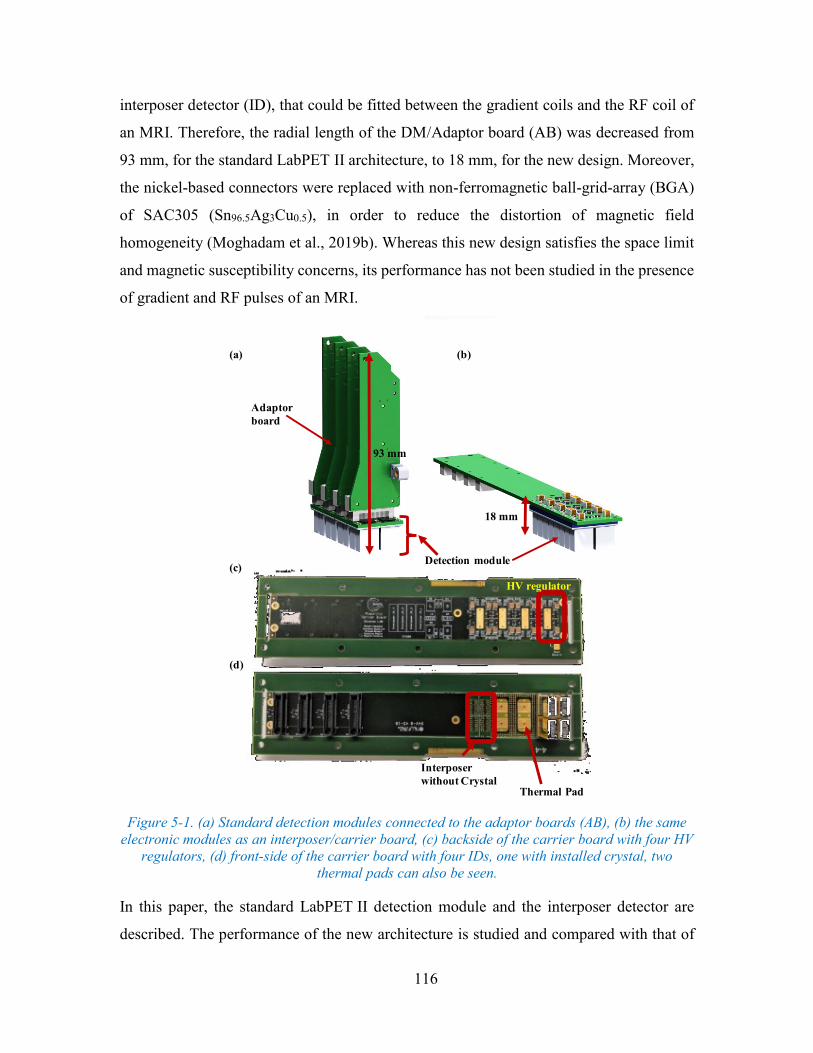
116
interposer detector (ID), that could be fitted between the gradient coils and the RF coil of
an MRI. Therefore, the radial length of the DM/Adaptor board (AB) was decreased from
93 mm, for the standard LabPET II architecture, to 18 mm, for the new design. Moreover,
the nickel-based connectors were replaced with non-ferromagnetic ball-grid-array (BGA)
of SAC305 (Sn96.5Ag3Cu0.5), in order to reduce the distortion of magnetic field
homogeneity (Moghadam et al., 2019b). Whereas this new design satisfies the space limit
and magnetic susceptibility concerns, its performance has not been studied in the presence
of gradient and RF pulses of an MRI.
Figure 5-1. (a) Standard detection modules connected to the adaptor boards (AB), (b) the same
electronic modules as an interposer/carrier board, (c) backside of the carrier board with four HV
regulators, (d) front-side of the carrier board with four IDs, one with installed crystal, two
thermal pads can also be seen.
In this paper, the standard LabPET II detection module and the interposer detector are
described. The performance of the new architecture is studied and compared with that of
HV regulator
Interposer
without CrystalThermal Pad
(a) (b)
Adaptor
board
18 mm
Detection module
93 mm
(c)
(d)
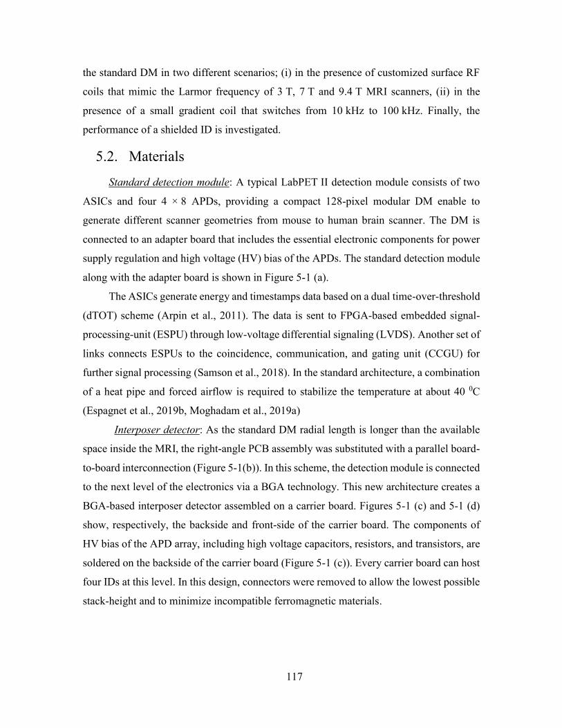
117
the standard DM in two different scenarios; (i) in the presence of customized surface RF
coils that mimic the Larmor frequency of 3 T, 7 T and 9.4 T MRI scanners, (ii) in the
presence of a small gradient coil that switches from 10 kHz to 100 kHz. Finally, the
performance of a shielded ID is investigated.
5.2. Materials
Standard detection module: A typical LabPET II detection module consists of two
ASICs and four 4 × 8 APDs, providing a compact 128-pixel modular DM enable to
generate different scanner geometries from mouse to human brain scanner. The DM is
connected to an adapter board that includes the essential electronic components for power
supply regulation and high voltage (HV) bias of the APDs. The standard detection module
along with the adapter board is shown in Figure 5-1 (a).
The ASICs generate energy and timestamps data based on a dual time-over-threshold
(dTOT) scheme (Arpin et al., 2011). The data is sent to FPGA-based embedded signal-
processing-unit (ESPU) through low-voltage differential signaling (LVDS). Another set of
links connects ESPUs to the coincidence, communication, and gating unit (CCGU) for
further signal processing (Samson et al., 2018). In the standard architecture, a combination
of a heat pipe and forced airflow is required to stabilize the temperature at about 40 0C
(Espagnet et al., 2019b, Moghadam et al., 2019a)
Interposer detector: As the standard DM radial length is longer than the available
space inside the MRI, the right-angle PCB assembly was substituted with a parallel board-
to-board interconnection (Figure 5-1(b)). In this scheme, the detection module is connected
to the next level of the electronics via a BGA technology. This new architecture creates a
BGA-based interposer detector assembled on a carrier board. Figures 5-1 (c) and 5-1 (d)
show, respectively, the backside and front-side of the carrier board. The components of
HV bias of the APD array, including high voltage capacitors, resistors, and transistors, are
soldered on the backside of the carrier board (Figure 5-1 (c)). Every carrier board can host
four IDs at this level. In this design, connectors were removed to allow the lowest possible
stack-height and to minimize incompatible ferromagnetic materials.
118
Figure 5-2. 3D view of Interposer detection module
A 3D view of the ID is displayed in Figure 5-2. The two gray rectangles are ASICs,
and the four small black squares are the voltage regulator ICs. ASICs are soldered with
the flip chip method on the interposer module. The ASICs are then sandwiched between
detection module and carrier boards for keeping them immune from EMI, thus, creating a
compact low profile assembly of 18 mm hight. The ASIC thickness is around 400 μm and
the diameter of a BGA (small gray spheres in Figure 5-2) based on the SAC305 solder
paste is 600 μm before the reflow process. The space available on the interposer and around
the ASICs make it possible to install thin components with a packaging size of 01005 (400
x 200 μm2) to design the voltage regulators.
The fully symmetrical design of the interposer detector, shown in Figure 5-2, and
its unique scheme provide a cost-effective solution to reduce the radial length of electronics
required for a PET-insert (Bouchard et al., 2019). In addition, this new design decreased
ferromagnetic materials in the MRI bore, which improves the magnetic field homogeneity.
The carrier board efficiently extracts the ~1172 mW heat, per each detector,
produced by the ASICs and the four voltage regulators, owing to the embedded thermal
pads designed on the front side of the carrier board, as displayed in Figure 5-1 (c) (Espagnet
et al., 2019a).
5.3. Methods
An interposer-carrier board was installed on the LabPET II technology test bench
to measure the baseline voltage, its RMS noise level, and the energy resolution. The analog
baseline voltage corresponds to the DC offset at the shaper output of the ASIC. The data
acquisitions were made with an 18.5 MBq 68Ge radioactive rod source. To have more
flexibility than inside MRI, RF and gradient coils were respectively designed based on the
119
Larmor frequency of high-magnetic field MRI scanners and the slew rate of the desired
gradient pulses. Subsequently, the tests were conducted in an MRI-like environment
instead of an MRI bore. Details of the custom-made RF and gradient coils can be found in
(Moghadam et al., 2019a).
Figure 5-3. The gradient coil surrounded a detector installed on interposer board. A standard
Adaptor board (AB) is also displayed.
The standard detection module of the LabPET II technology was then installed on
the same test-bench and identical tests were carried out to evaluate the performance of the
standard DM.
5.3.1. RF Coil Effects on the Interposer Detector
The hexagonal surface RF coil was placed parallel to top of the crystals /ASICs in a
set-up similar to figure 5-3 at a 10 mm distance. The average voltage of the baseline, the
RMS noise level, and the energy spectra were measured without and with RF coil pulses
corresponding to 3 T (127.74 MHz), 7 T (298 MHz), and 9.4 T (400.25 MHz) MRI
Carrier board
Crystal array
Gradient coil
Standard AB
Low-profile DM
120
frequencies. The same experiments were conducted on the standard LabPET II detection
module.
Since, in the LabPET II scanner, the data is processed based on the dTOT scheme,
the energy resolution was measured and presented in TOT bin. It is relevant to mention
that the energy resolution in the keV range has an exponential relation with the TOT bin.
Nonetheless, in this study, the comparison between the two values in bin is sufficient to
examine the behavior of the ID in the presence of the MRI signals. For energy resolution
measurements, a Gaussian fit of the energy spectrum photopeak was used. The energy
resolution is defined as the full width at half maximum (FWHM) of the Gaussian fit.
5.3.2. Gradient Coil Effects on the Interposer Detector
The gradient coil with a maximum slew rate of 260 mT/m/s surrounded one IDs, as
shown in Figure 5-3 (b). The average voltage of the baseline, the RMS noise, and the
energy spectra were evaluated without and with gradient switching at 10 kHz, 50 kHz, and
100 kHz. The same measurements were conducted for the standard DM and the results
were compared to the performance of the ID.
5.3.3. Eliminating the Interferences
To eliminate the remaining EMI interferences in both high and low frequencies, a
0.1 mm thick layer of CHO-SHIELD® 2056 paint was wrapped around the
interposer/carrier board. To eliminate any possibility of short circuit owing to conductive
layer of shiedling composite, the CHO-SHIELD® 2056 paint with uniformity of ±5% was
deposited over a 0.18 mm thick electrical tape (TEMFLEX-3/4X60). The shielding layer
was connected to the ground-plane of the carrier board to establish a common ground. This
paint offers a shielding effectiveness (SE) of 80 dB and 65 dB in the megahertz and
kilohertz frequency ranges, respectively (Parker-Chomerics, 2019). The noise added to the
impulse response of the ASIC analog chain and the baseline noise were measured for an
ID, with and without the shielding layer, in the presence of RF signals and gradient
switching pulses.
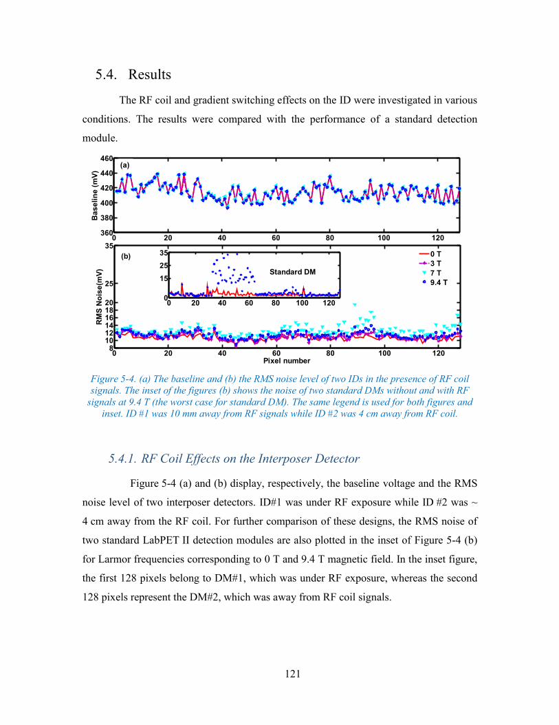
121
5.4. Results
The RF coil and gradient switching effects on the ID were investigated in various
conditions. The results were compared with the performance of a standard detection
module.
Figure 5-4. (a) The baseline and (b) the RMS noise level of two IDs in the presence of RF coil
signals. The inset of the figures (b) shows the noise of two standard DMs without and with RF
signals at 9.4 T (the worst case for standard DM). The same legend is used for both figures and
inset. ID #1 was 10 mm away from RF signals while ID #2 was 4 cm away from RF coil.
5.4.1. RF Coil Effects on the Interposer Detector
Figure 5-4 (a) and (b) display, respectively, the baseline voltage and the RMS
noise level of two interposer detectors. ID#1 was under RF exposure while ID #2 was ~
4 cm away from the RF coil. For further comparison of these designs, the RMS noise of
two standard LabPET II detection modules are also plotted in the inset of Figure 5-4 (b)
for Larmor frequencies corresponding to 0 T and 9.4 T magnetic field. In the inset figure,
the first 128 pixels belong to DM#1, which was under RF exposure, whereas the second
128 pixels represent the DM#2, which was away from RF coil signals.
0 20 40 60 80 100 120360
380
400
420
440
460
Ba
se
lin
e (
mV
)
0 20 40 60 80 100 1208
101214161820
25
35
Pixel number
RM
S N
ois
e(m
V)
0 20 40 60 80 100 1200
15
25
35
0 T
3 T
7 T
9.4 T
(a)
(b)
Standard DM
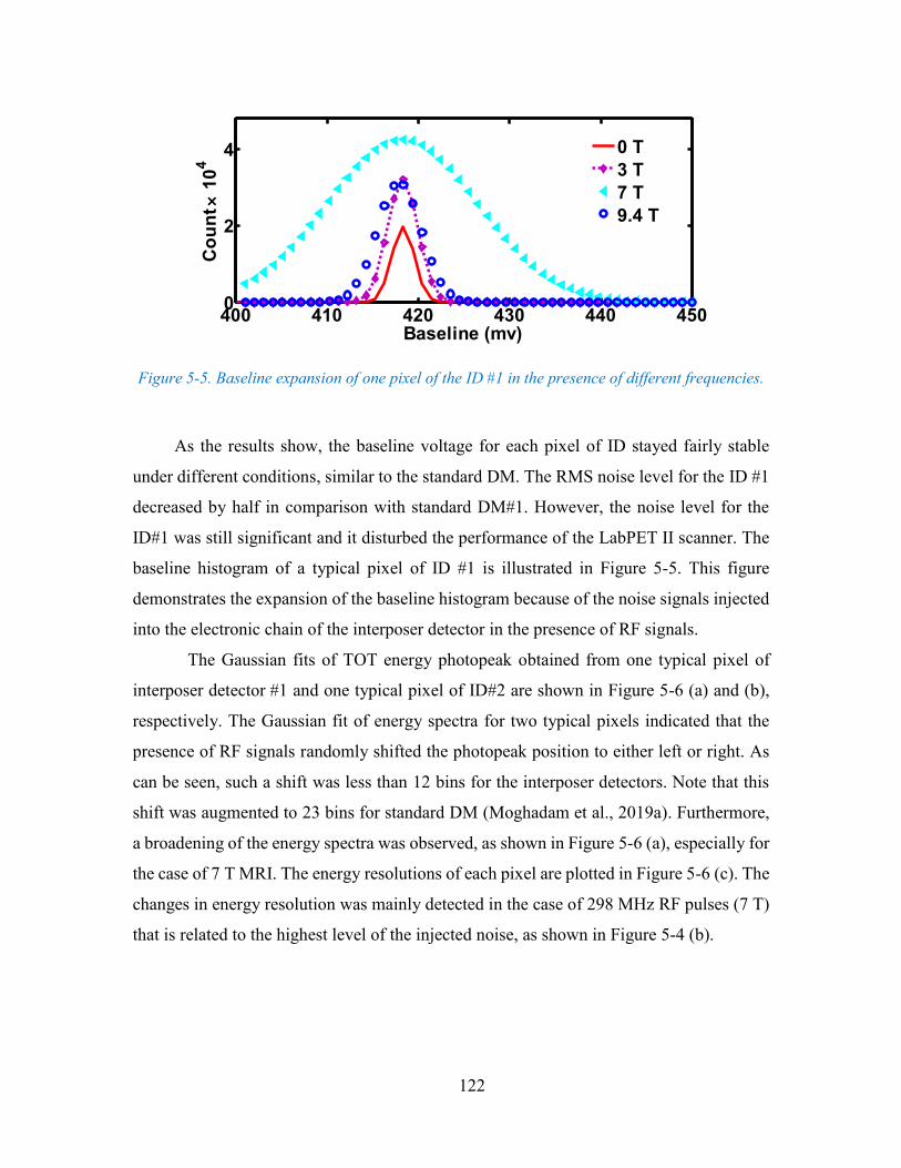
122
Figure 5-5. Baseline expansion of one pixel of the ID #1 in the presence of different frequencies.
As the results show, the baseline voltage for each pixel of ID stayed fairly stable
under different conditions, similar to the standard DM. The RMS noise level for the ID #1
decreased by half in comparison with standard DM#1. However, the noise level for the
ID#1 was still significant and it disturbed the performance of the LabPET II scanner. The
baseline histogram of a typical pixel of ID #1 is illustrated in Figure 5-5. This figure
demonstrates the expansion of the baseline histogram because of the noise signals injected
into the electronic chain of the interposer detector in the presence of RF signals.
The Gaussian fits of TOT energy photopeak obtained from one typical pixel of
interposer detector #1 and one typical pixel of ID#2 are shown in Figure 5-6 (a) and (b),
respectively. The Gaussian fit of energy spectra for two typical pixels indicated that the
presence of RF signals randomly shifted the photopeak position to either left or right. As
can be seen, such a shift was less than 12 bins for the interposer detectors. Note that this
shift was augmented to 23 bins for standard DM (Moghadam et al., 2019a). Furthermore,
a broadening of the energy spectra was observed, as shown in Figure 5-6 (a), especially for
the case of 7 T MRI. The energy resolutions of each pixel are plotted in Figure 5-6 (c). The
changes in energy resolution was mainly detected in the case of 298 MHz RF pulses (7 T)
that is related to the highest level of the injected noise, as shown in Figure 5-4 (b).
400 410 420 430 440 4500
2
4
Baseline (mv)
Co
un
t
10
4
pixel 8 detection module 1 interposer under direct tension
0 T
3 T
7 T
9.4 T
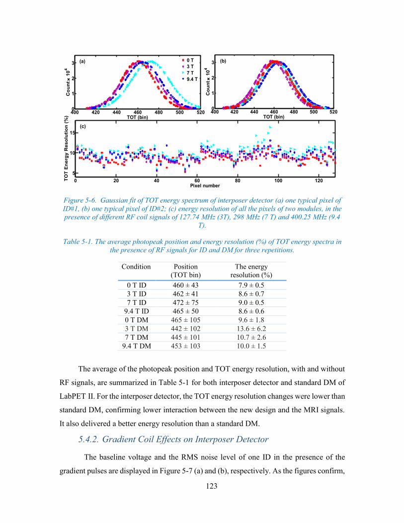
123
Figure 5-6. Gaussian fit of TOT energy spectrum of interposer detector (a) one typical pixel of
ID#1, (b) one typical pixel of ID#2; (c) energy resolution of all the pixels of two modules, in the
presence of different RF coil signals of 127.74 MHz (3T), 298 MHz (7 T) and 400.25 MHz (9.4
T).
Table 5-1. The average photopeak position and energy resolution (%) of TOT energy spectra in
the presence of RF signals for ID and DM for three repetitions.
Condition Position
(TOT bin)
The energy
resolution (%)
0 T ID 460 ± 43 7.9 ± 0.5
3 T ID 462 ± 41 8.6 ± 0.7
7 T ID 472 ± 75 9.0 ± 0.5
9.4 T ID 465 ± 50 8.6 ± 0.6
0 T DM 465 ± 105 9.6 ± 1.8
3 T DM 442 ± 102 13.6 ± 6.2
7 T DM 445 ± 101 10.7 ± 2.6
9.4 T DM 453 ± 103 10.0 ± 1.5
The average of the photopeak position and TOT energy resolution, with and without
RF signals, are summarized in Table 5-1 for both interposer detector and standard DM of
LabPET II. For the interposer detector, the TOT energy resolution changes were lower than
standard DM, confirming lower interaction between the new design and the MRI signals.
It also delivered a better energy resolution than a standard DM.
5.4.2. Gradient Coil Effects on Interposer Detector
The baseline voltage and the RMS noise level of one ID in the presence of the
gradient pulses are displayed in Figure 5-7 (a) and (b), respectively. As the figures confirm,
400 420 440 460 480 500 5200
1
2
3
TOT (bin)
Co
un
t
10
4
400 420 440 460 480 500 5200
1
2
3
TOT (bin)
Co
un
t
10
4
0 20 40 60 80 100 120
5
10
15
Pixel number
TO
T E
ne
rgy
Re
so
luti
on
(%
)0 T
3 T
7 T
9.4 T
(a) (b)
(c)
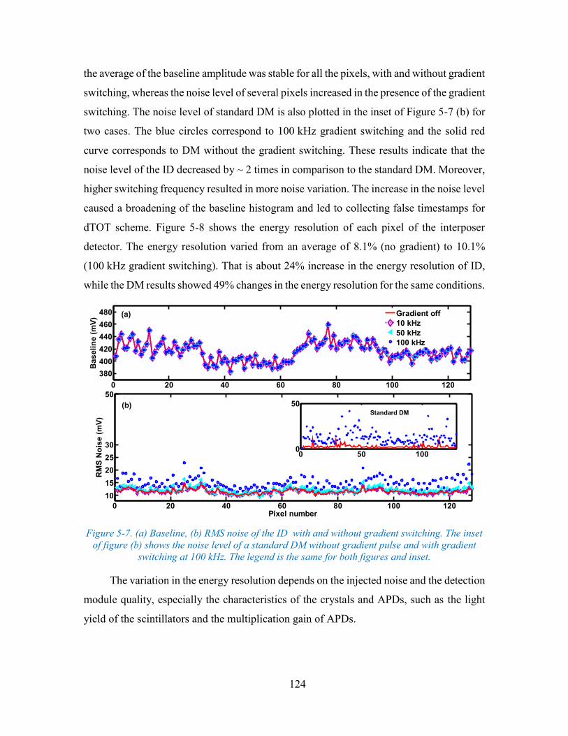
124
the average of the baseline amplitude was stable for all the pixels, with and without gradient
switching, whereas the noise level of several pixels increased in the presence of the gradient
switching. The noise level of standard DM is also plotted in the inset of Figure 5-7 (b) for
two cases. The blue circles correspond to 100 kHz gradient switching and the solid red
curve corresponds to DM without the gradient switching. These results indicate that the
noise level of the ID decreased by ~ 2 times in comparison to the standard DM. Moreover,
higher switching frequency resulted in more noise variation. The increase in the noise level
caused a broadening of the baseline histogram and led to collecting false timestamps for
dTOT scheme. Figure 5-8 shows the energy resolution of each pixel of the interposer
detector. The energy resolution varied from an average of 8.1% (no gradient) to 10.1%
(100 kHz gradient switching). That is about 24% increase in the energy resolution of ID,
while the DM results showed 49% changes in the energy resolution for the same conditions.
Figure 5-7. (a) Baseline, (b) RMS noise of the ID with and without gradient switching. The inset
of figure (b) shows the noise level of a standard DM without gradient pulse and with gradient
switching at 100 kHz. The legend is the same for both figures and inset.
The variation in the energy resolution depends on the injected noise and the detection
module quality, especially the characteristics of the crystals and APDs, such as the light
yield of the scintillators and the multiplication gain of APDs.
0 20 40 60 80 100 120
380
400
420
440
460
480
Ba
se
lin
e (
mV
)
0 20 40 60 80 100 120
10
15
20
25
30
50
Pixel number
RM
S N
ois
e (
mV
)
Gradient off
10 kHz
50 kHz
100 kHz
0 50 1000
50
(a)
(b)Standard DM
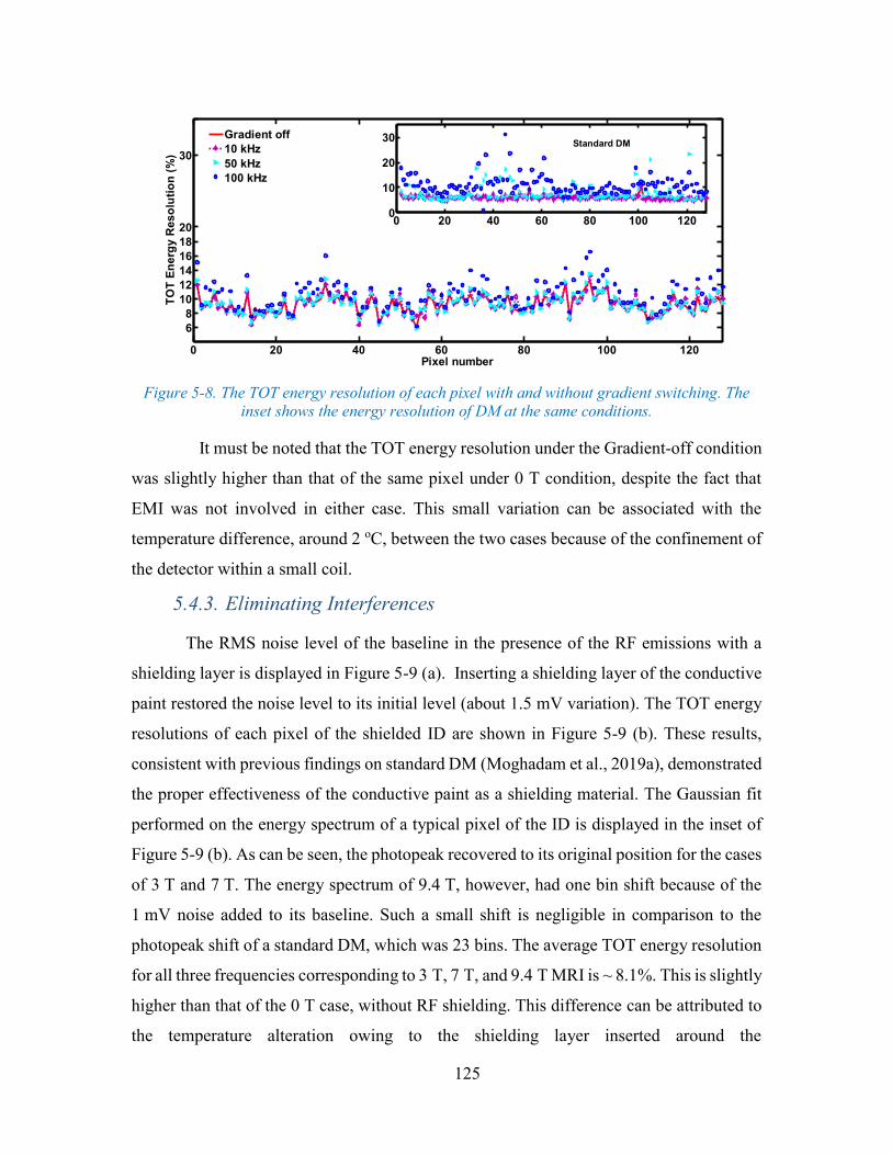
125
Figure 5-8. The TOT energy resolution of each pixel with and without gradient switching. The
inset shows the energy resolution of DM at the same conditions.
It must be noted that the TOT energy resolution under the Gradient-off condition
was slightly higher than that of the same pixel under 0 T condition, despite the fact that
EMI was not involved in either case. This small variation can be associated with the
temperature difference, around 2 oC, between the two cases because of the confinement of
the detector within a small coil.
5.4.3. Eliminating Interferences
The RMS noise level of the baseline in the presence of the RF emissions with a
shielding layer is displayed in Figure 5-9 (a). Inserting a shielding layer of the conductive
paint restored the noise level to its initial level (about 1.5 mV variation). The TOT energy
resolutions of each pixel of the shielded ID are shown in Figure 5-9 (b). These results,
consistent with previous findings on standard DM (Moghadam et al., 2019a), demonstrated
the proper effectiveness of the conductive paint as a shielding material. The Gaussian fit
performed on the energy spectrum of a typical pixel of the ID is displayed in the inset of
Figure 5-9 (b). As can be seen, the photopeak recovered to its original position for the cases
of 3 T and 7 T. The energy spectrum of 9.4 T, however, had one bin shift because of the
1 mV noise added to its baseline. Such a small shift is negligible in comparison to the
photopeak shift of a standard DM, which was 23 bins. The average TOT energy resolution
for all three frequencies corresponding to 3 T, 7 T, and 9.4 T MRI is ~ 8.1%. This is slightly
higher than that of the 0 T case, without RF shielding. This difference can be attributed to
the temperature alteration owing to the shielding layer inserted around the
0 20 40 60 80 100 120
6
8
10
12
14
16
18
20
30
Pixel number
TO
T E
ne
rgy
Re
so
luti
on
(%
)
Gradient off
10 kHz
50 kHz
100 kHz
0 20 40 60 80 100 1200
10
20
30
Standard DM
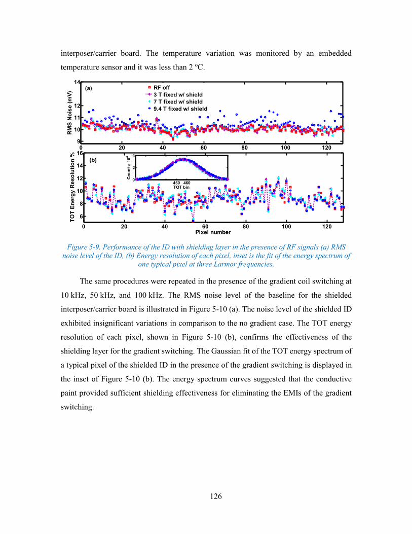
126
interposer/carrier board. The temperature variation was monitored by an embedded
temperature sensor and it was less than 2 oC.
Figure 5-9. Performance of the ID with shielding layer in the presence of RF signals (a) RMS
noise level of the ID, (b) Energy resolution of each pixel, inset is the fit of the energy spectrum of
one typical pixel at three Larmor frequencies.
The same procedures were repeated in the presence of the gradient coil switching at
10 kHz, 50 kHz, and 100 kHz. The RMS noise level of the baseline for the shielded
interposer/carrier board is illustrated in Figure 5-10 (a). The noise level of the shielded ID
exhibited insignificant variations in comparison to the no gradient case. The TOT energy
resolution of each pixel, shown in Figure 5-10 (b), confirms the effectiveness of the
shielding layer for the gradient switching. The Gaussian fit of the TOT energy spectrum of
a typical pixel of the shielded ID in the presence of the gradient switching is displayed in
the inset of Figure 5-10 (b). The energy spectrum curves suggested that the conductive
paint provided sufficient shielding effectiveness for eliminating the EMIs of the gradient
switching.
0 20 40 60 80 100 1209
10
11
12
14
RM
S N
ois
e (
mV
)
0 20 40 60 80 100 120
6
8
10
12
14
16
Pixel number
TO
T E
ne
rgy
Re
so
luti
on
%
RF off
3 T fixed w/ shield
7 T fixed w/ shield
9.4 T fixed w/ shield
450 4600
2
4
TOT bin
Co
un
t 1
04
(a)
(b)
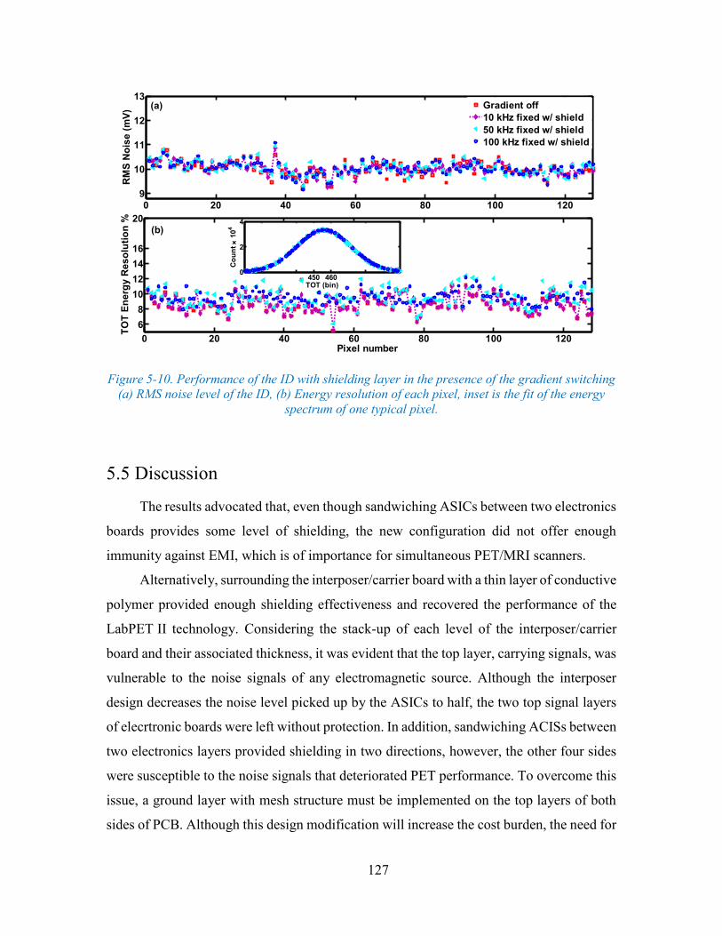
127
Figure 5-10. Performance of the ID with shielding layer in the presence of the gradient switching
(a) RMS noise level of the ID, (b) Energy resolution of each pixel, inset is the fit of the energy
spectrum of one typical pixel.
5.5 Discussion
The results advocated that, even though sandwiching ASICs between two electronics
boards provides some level of shielding, the new configuration did not offer enough
immunity against EMI, which is of importance for simultaneous PET/MRI scanners.
Alternatively, surrounding the interposer/carrier board with a thin layer of conductive
polymer provided enough shielding effectiveness and recovered the performance of the
LabPET II technology. Considering the stack-up of each level of the interposer/carrier
board and their associated thickness, it was evident that the top layer, carrying signals, was
vulnerable to the noise signals of any electromagnetic source. Although the interposer
design decreases the noise level picked up by the ASICs to half, the two top signal layers
of elecrtronic boards were left without protection. In addition, sandwiching ACISs between
two electronics layers provided shielding in two directions, however, the other four sides
were susceptible to the noise signals that deteriorated PET performance. To overcome this
issue, a ground layer with mesh structure must be implemented on the top layers of both
sides of PCB. Although this design modification will increase the cost burden, the need for
0 20 40 60 80 100 120
9
10
11
12
13
RM
S N
ois
e (
mV
)
Gradient off
10 kHz fixed w/ shield
50 kHz fixed w/ shield
100 kHz fixed w/ shield
0 20 40 60 80 100 120
6
8
10
12
14
16
20
Pixel number
TO
T E
ne
rgy
Re
so
luti
on
%
450 4600
2
4
TOT (bin)
Co
un
t 1
04
(a)
(b)
128
shielding will be probablly eliminated for the alternative architecture based on the
interposer detector. Considering the small area of each ground layer and the small gap
between adjacent boards, this new design would act as a mesh shielding configuration for
both frequency ranges. Thus the level of induced eddy currents will decrease, providing
the feasibility to acquire the MRI sequences with a fast gradient switching.
5.6. Conclusion
In this paper, the effects of the RF and gradient coil interferences on the interposer
detector based on LabPET II technology were investigated. The results demonstrated the
feasibility of using an interposer detector to realize a simultaneous PET/MRI scanner with
a sub-millimeter spatial resolution for mouse and rabbit preclinical applications. However,
on each side of the PCB board, the top layer was left without EMI protection. Therefore,
the signals in those layers were distorted with MRI pulses. The interposer/carrier board
offers high thermal performance; thus, the temperature variation effects on the interposer
detector performance were less significant than the standard detection module. The average
energy resolution for interposer detector improves four times and the average noise level
of baseline voltage decreases by two-order of magnitude in comparision to the standard
detection module. For both RF signals and gradient switching, the CHO-SHIELD® 2056
paint, as an EMI shielding layer, was able to eliminate the EMI effects that degrade the
performance of the interposer detector, designed based on LabPET II technology. For
further improvement of the interposer performance, the ground layer has to be implemented
on the top and bottom layers, which increases the cost related to the fabrication of new
boards. Therefore, it stands to reason that developing a shielding layer is more attractive
both commercially and technically compared to such comprehensive designs.
Acknowledgment
This work was supported by Fonds de recherche du Québec – Nature et technologies
(FRQNT) and Natural Sciences and Engineering Research Council of Canada (NSERC)
funds.
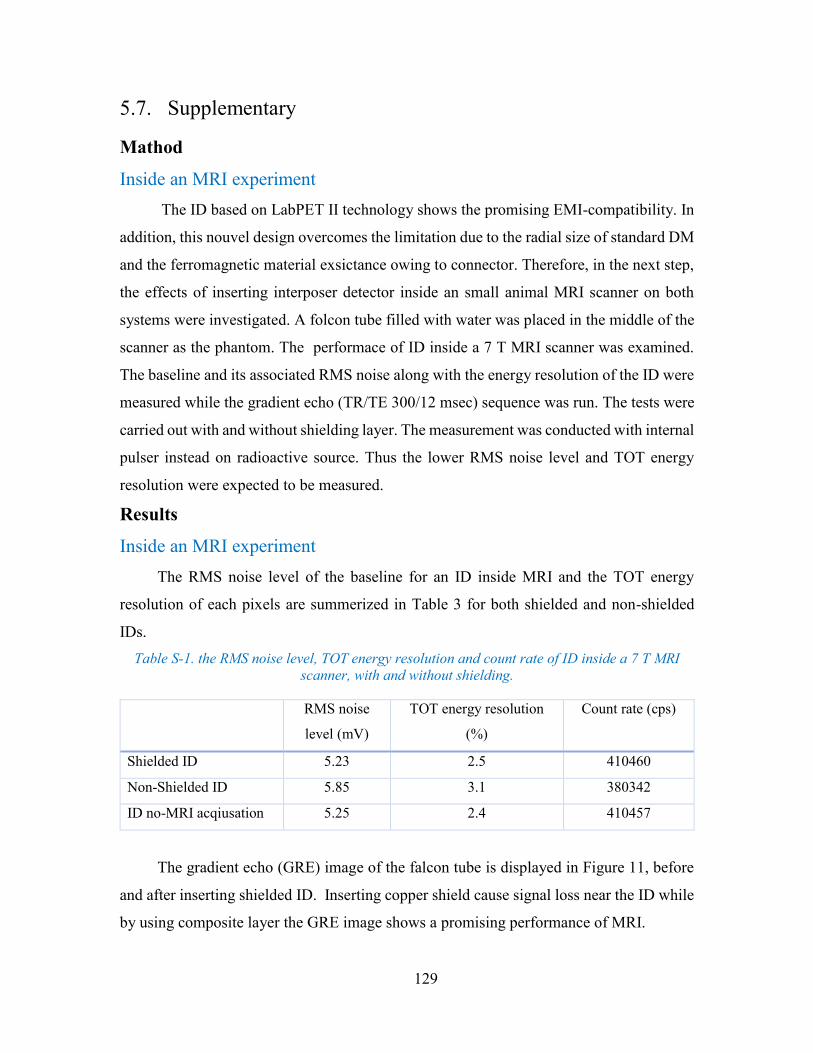
129
5.7. Supplementary
Mathod
Inside an MRI experiment
The ID based on LabPET II technology shows the promising EMI-compatibility. In
addition, this nouvel design overcomes the limitation due to the radial size of standard DM
and the ferromagnetic material exsictance owing to connector. Therefore, in the next step,
the effects of inserting interposer detector inside an small animal MRI scanner on both
systems were investigated. A folcon tube filled with water was placed in the middle of the
scanner as the phantom. The performace of ID inside a 7 T MRI scanner was examined.
The baseline and its associated RMS noise along with the energy resolution of the ID were
measured while the gradient echo (TR/TE 300/12 msec) sequence was run. The tests were
carried out with and without shielding layer. The measurement was conducted with internal
pulser instead on radioactive source. Thus the lower RMS noise level and TOT energy
resolution were expected to be measured.
Results
Inside an MRI experiment
The RMS noise level of the baseline for an ID inside MRI and the TOT energy
resolution of each pixels are summerized in Table 3 for both shielded and non-shielded
IDs.
Table S-1. the RMS noise level, TOT energy resolution and count rate of ID inside a 7 T MRI
scanner, with and without shielding.
RMS noise
level (mV)
TOT energy resolution
(%)
Count rate (cps)
Shielded ID 5.23 2.5 410460
Non-Shielded ID 5.85 3.1 380342
ID no-MRI acqiusation 5.25 2.4 410457
The gradient echo (GRE) image of the falcon tube is displayed in Figure 11, before
and after inserting shielded ID. Inserting copper shield cause signal loss near the ID while
by using composite layer the GRE image shows a promising performance of MRI.
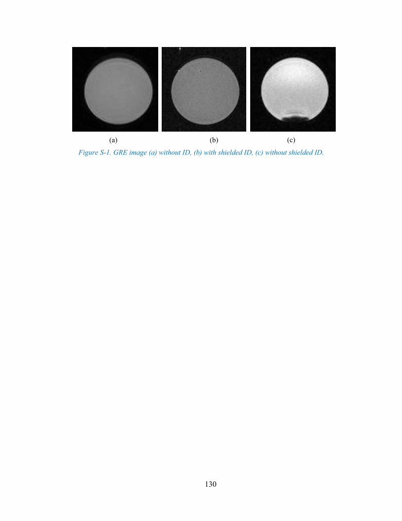
130
(a) (b)
(c)
Figure S-1. GRE image (a) without ID, (b) with shielded ID, (c) without shielded ID.

131
132
CHAPTER 6
CNT-COMPOSITE SHIELDING
Avant-propos
Auteurs et Affiliation:
Narjes Moghadam: étudiante au doctorat, Institut interdisciplinaire
d’innovation technologique - 3IT, Université de Sherbrooke, Faculté de génie,
Département de génie électrique et de génie informatique.
Roger Lecomte: professeur, Université de Sherbrooke, Département de
médecine nucléaire et de radiobiologie
Réjean Fontaine: professeur, Institut interdisciplinaire d’innovation
technologique - 3IT, Université de Sherbrooke, Faculté de génie, Département
de génie électrique et de génie informatique.
Date d’acceptation : xxx
État de l’acceptation : prepared to be submitted
Revue : IEEE Transactions on Nanotechnology
Titre français : Blindage d'interférence électromagnétique pour TEP/IRM simultanée à
l'aide d'un composite ultra-mince de nanotubes de carbone
Contribution au document :
C'est le quatrième article dans lequel nous évaluons la possibilité d'utiliser un
composite de nanotubes de carbone (CNT) comme couche de protection pour réduire les
effets des courants de Foucault et favoriser la compatibilité TEP/IRM. Pour ce faire, nous
devons parvenir à créer un polymère hautement conducteur présentant une structure
homogène. En raison des propriétés spécifiques du composite, notre nouveau composite
bloque les basses fréquences de manière appropriée et diminue considérablement les
courants de Foucault. Dans cet article, le processus de fabrication du composite CNT ainsi
que la méthode de caractérisation ont été expliqués. Le composite CNT ayant les propriétés
souhaitées a été choisi et utilisé comme blindage placé entre le module de détection
LabPET II et une bobine d’IRM. Les performances du module de détection LabPET II ont
été caractérisées avec la nouvelle configuration de blindage.
133
Résumé en français:
Les nanotubes de carbone ont montré des propriétés prometteuses en tant que
matériau de remplissage pour augmenter la conductivité électrique des composites. Ils ont
été utilisé pour la fabrication de composites de blindage à haute fréquence, mais ses
propriétés à basse fréquence n’ont pas été entièrement caractérisées. Dans cette étude, un
composite à base de polydiméthylsiloxane (PDMS) et de nanotubes de carbone (CNT) a
été fabriqué pour éliminer l’impact des interférences électromagnétiques à basse fréquence
dans les scanners de TEP/IRM. Pour fabriquer une solution composite homogène, nous
avons combiné les méthodes d’ultra-sonication et de mélange à cisaillement. La mesure de
l'impédance a confirmé qu'un composite fabriqué par ce procédé de traitement fournit la
conductivité requise pour le blindage contre les interférences électromagnétiques dans la
plage de fréquences souhaitée. Les résultats démontrent qu’en utilisant ce composite, les
interférences dues au gradient de l’IRM pourraient être largement éliminées pour les
performances d’un scanner basé sue le module de détection LabPET II, tel que démontré
en mesurant la résolution énergétique et temporelle des détecteurs LabPET II.
Mots clés: Composite de nanotubes de carbone, conductivité électrique, blindage
électromagnétique, interférences à basse fréquence, scanner TEP / IRM
Contribution of this document to the thesis (English):
This is the last article in which we evaluate the possibility of utilizing carbon nanotube
(CNT) composites as a shielding layer to decrease the eddy current effects on PET/MRI.
For that purpose, we need to reach a high conductive polymer with high homogeneity.
Owing to the specific properties of the CNT composite, our new material shields the low
frequency appropriately and decreases the eddy current significantly. In this paper, the
fabrication process of CNT composite, along with the characterization method, was
explained. The CNT composite with the desired properties was developed and used as the
shielding layer placed between LabPET II detection modules and MRI coils. The
performance of the LabPET II detection module was assessed using the new shielding
configuration.
*The content maybe different from the published one.
134
Electromagnetic Interference Shielding of
Simultaneous PET/MRI Using Ultra-Thin
Carbon-Nanotube Composite
Abstract— Carbon nanotube has shown promising properties as a filler for
increasing the electrical conductivity of composites. It has been used for fabricating
shielding composite for gigahertz frequency range. However, its properties in low
frequencies are still unknown. In this study, composite layers based on carbon nanotube
(CNT)-Polydimethylsiloxane (PDMS) have been synthesized. Both multi-wall Carbon
nanotube and single-wall carbon nanotube were examined to find the appropriate
composite for eliminating the impact of low-frequency electromagnetic interferences on
PET/MRI scanner. The CNT dispersibility was studied in various solvents. To fabricate a
homogeneous composite, we combined the ultra-sonication and the shear mixing methods.
The impedance measurements confirmed that a well-processed composite provides the
required conductivity for EMI shielding at the desired frequency range. The results
demonstrated that using this composite, the EMI effects due to the MRI’s gradient and RF
coils can be compensated on LabPET II scanner performances.
Keyword: CNT composite, electrical conductivity, electromagnetic shielding, low-
frequency interferences, PET/MRI scanner
6.1. Introduction
In the presence of electromagnetic fields, the performance of electronic devices fails
because of electromagnetic interferences (EMI). Electromagnetic fields at high frequency
are efficiently shielded using metallic materials, such as copper and aluminum, or
conductive composites (Jagatheesan et al., 2014). Typically, a sheet of these materials with
135
a thickness of some micrometer or a mesh of them with hole size designed for the desired
frequency is used to achieve the required shielding effectiveness (SE) at high frequencies
(Peng et al., 2010, Kang et al., 2009). For low-frequency shielding, however, a thicker layer
of metal must be employed, hence the weight and the cost of such an interface increases.
In the case of static or slowly changing magnetic fields, a Faraday cage is ineffective;
instead, high-magnetic permeability materials, such as Permalloy and Mu-Metal sheets, or
ferromagnetic metal coatings with nanocrystalline grain structure are commonly used
(Conecici et al., 2017). High-magnetic permeability materials redirect magnetic fields and
protect sensitive devices. On this subject, Livesey et al. synthesized a composite, made of
magnetic nanoparticles embedded in a polymer matrix, to shield low frequencies at several
hundred kHz (Livesey et al., 2017).
Designing a fully integrated positron emission tomography/magnetic resonance
imaging (PET/MRI) scanner necessitates eliminating all the electromagnetic interferences
between the two modalities without degrading the overall performance of each scanner.
However, the use of shielding layers based on metallic or high-magnetic permeability
materials inside MRI scanners is impractical, since they distort the MR image quality
(Koch et al., 2010). In this respect, the gradient coil of MRI is the primary source of low-
frequency interferences. Indeed, the amplitude of the gradient field is smaller than that of
the main magnetic field. Nonetheless, it switches very fast and induces eddy currents in
any closed electric and conductive path, as explained by Faraday’s law. These eddy
currents affect the performance of an electronic device by generating heat. Besides, based
on Lenz law, they produce reverse magnetic fields that distort the gradient field and cause
MR image artifacts.
Regarding the PET scanner, the accuracy of acquisition signals is of high importance
to obtain precise images, which necessitates implementing a compatible shielding layer in
the PET/MRI scanner to eliminate the effect of the low-frequency electromagnetic field of
the gradient on the PET electronics. Otherwise, the low-frequency signals increase the
temperature of the PET electronics, change the APD gain and disturbs the detection module
performance; consequently, data will be lost, and timing resolution will be increased
(Düppenbecker et al., 2016, Moghadam et al., 2019a).
136
Another effect of the gradient field on the PET scanner is the distortion of energy
resolution because of the instability of the bias voltage of APD during gradient switching
(Düppenbecker et al., 2016). Such uncertainty changes the photoelectron statistic and
decreases the count rate that, in turn, increases the statistical noise and deteriorates the
energy resolution.
To date, for PET/MRI applications, two types of shielding materials have mainly
been reported. The first type is metallic shielding made of copper or aluminum that has
been commonly used in commercial PET/MRI systems (Kang et al., 2009). The second
one is carbon fiber shielding, which has recently been proposed by two research groups
from UC Davis (Peng et al., 2014a) and Aachen University (Düppenbecker et al., 2012).
Kang et al. examined metallic shielding with plate and mesh structures (Kang et al.,
2009). They reported that the plate configuration, with only 30-micrometer thickness,
provided sufficient shielding effectiveness (SE) for one PET module. However, by
increasing the area of the copper plate inside the MRI bore, to cover the whole system,
both signal-to-noise ratio (SNR) and homogeneity of MRI were deteriorated, and the
temperature inside the MRI was augmented. Alternatively, the mesh structure offered a
better homogeneity and SNR, but a lower SE compared to the plate configuration.
Peng et al. conducted a chemical shift artifact (CSA) protocol to determine the eddy
current effects in the MR image (Peng et al., 2010). By comparing different thicknesses of
the copper plate, they demonstrated that the chemical shift artifact increases by the
thickness of the metallic materials located inside the field of view (FOV) of the MR bore
and, as a result, the induction of the eddy current increases. In 2014, the same research
group investigated the CSA data for carbon fiber. It was shown that, although the carbon
fiber provided enough SE against RF coil signal, the gradient effect still could not be
eliminated without inserting a thin copper foil between PET and gradient (Peng et al.,
2014a). Subsequently, the eddy current was induced in MRI, as confirmed by frequency
shift. However, such artifacts were only significant in the case of fast imaging sequences.
Since the precedent studies established that metallic materials inevitably deteriorated
the performance of PET/MRI, some researches were directed toward other non-metallic
shielding layess. For instance, Parl et al. used polymer-based conductive foils as an
optically transparent RF shielding. In their study, ITO and 9900 foils were compared with
137
a copper-wire mesh, and the results were in favor of mesh structure (Parl et al., 2017). The
preceding discussion underlines that, despite the outstanding outcomes of previous
researches, finding an effective shielding layer without inducing eddy currents is still an
ongoing challenge.
In the communication network research, nanocomposite materials grabbed the
attention of researchers as an appealing candidate to substitute metallic shielding in the
GHz range. As for their advantages over metals, nanocomposites offer flexibility,
resistance to corrosion, lightweight, cost-effectiveness, and simple synthesis process
(González et al., 2016). In this regard, the unique structure and specific properties of carbon
nanotube (CNT), namely high aspect ratio, high thermal/electrical conductivity and
excellent tensile strength, make it a viable filling for shielding composite. Besides, CNT
has unique electronic-transport properties and optoelectronic-response characteristics
(Avouris et al., 2003, Aziziyan et al., 2012a, Aziziyan et al., 2012b, Moghadam et al., 2012,
Moghadam et al., 2013). CNTs have been previously utilized in several composites to
improve their thermal (Tan et al., 2013, Huang et al., 2014) and electrical (Zhou et al.,
2008, Wang et al., 2013, Kim et al., 2018, Logakis et al., 2011) properties.
Moreover, SE values of composites based on single-wall CNT (SWNT) and multi-
wall CNT (MWNT) for shielding of electromagnetic interferences at different frequencies
have been measured by several groups (Kim et al., 2004, Yang et al., 2005, Li et al., 2006,
Park et al., 2010, Kim et al., 2013, Sun et al., 2016). It has been reported that the SWNT-
composite provides proper shielding at low frequency, whereas MWNT-composite has
high conductivity at high frequencies up to 14 GHz. Compared to carbon black and carbon
fiber, CNT provided a higher electrical conductivity and a better SE (Cheng et al., 2010).
Nevertheless, SE of these nanocomposites is not sufficient for shielding EMI in PET/MRI
scanners. Some approaches were applied for improving the SE of the CNT based
composites, for instance using higher weight percent of CNT, employing CNT with higher
aspect ratio, annealing process to decrease wall defects and functionalizing CNT (Kim et
al., 2004, Logakis et al., 2011, Kim et al., 2018). Increasing the weight percentage of CNT
to 15%, enhanced the SE up to 49 dB (Li et al., 2006), while an actual EMI shielding for
PET/MRI uses must provide at least 60 dB of SE (Berneking et al., 2017). Despite the
promising potential of CNT based composites for shielding interferences up to GHz range
138
frequencies, it has never been applied for PET/MRI applications, primarily due to the low
conductivity of current nanocomposites at low frequencies.
In this paper, we have proposed and investigated a synthesis process for the
fabrication of new CNT composites for eliminating the interferences originating from low-
frequency switching signals of MRI gradients that affected LabPET II electronics. To
obtain the required SE, high dispersion of CNT in the solvent is crucial. Different organic
solvents were examined, and the most effective one was selected to synthesize the
nanocomposite. The goal was to eliminate both EMI and eddy current effects for PET/MRI
scanner. Four probe measurement data showed that the proposed nanocomposite could
achieve reasonable electrical conductivity for EMI shielding in the range of 1 kHz to
100 kHz, the typical gradient frequency range, while it was also capable of blocking RF
coil signals.
6.2. Materials and Methods
6.2.1. Materials
The MWNT with an outer diameter of 10–20 nm, length of 10–30 µm and purity of
95% as well as the SWNT with a diameter of 1–4 nm, a length of 5–30 µm and purity of
60% were purchased from Cheap Tubes Company. The elastomer of a 2-component
Polydimethylsiloxane (PDMS) from Dow Corning (SYLGARD 184) with a 10:1 base to
curing agent mixing ratio was used. Various solvents including Chlorobenzene (from J.T.
Baker), Isopropyl alcohol (IPA), Chloroform, Toluene (All from Fisher scientific) were
examined to determine the level of dispersion of the carbon nanotubes and the best solvent
for the synthesis process of nano-composite.
6.2.2. Synthesize Process of Nano-Composite
The Synthesis of the CNT based composite materials requires the careful formulation
of fabrication procedures to produce composites with appropriate characteristics. Because
of the CNT aggregation, attributed to the strong van der Waal binding, uniform dispersion
of CNT has been a complicated processing step. To prepare this composite, we used the
ultra-sonication method along with the shear mixing technique (Huang et al., 2006). Each
time a weight percent of CNT was added to the solvent and mixed using the sonication
139
processor (Cole-Parmer ®) for 30 min with 20 kHz frequency and 100 W power. This
process provides a uniform CNT-solution without agglomeration as it supplies energy
higher than the binding energy of an aggregated mixture, at the same time, lower than the
energy value that fractures a CNT. Then, PDMS was diluted in the desired solvent, and
this mixture was added to the CNT-solution. Afterward, they were mixed for 15 min using
ultra-sonication, followed by 6-h shear mixing at 500 rpm. The sample was placed under a
fume hood overnight to evaporate the solvent. In the next step, part B of the PDMS kit has
been added and mixed rigorously. The composite was put into a vacuum chamber for 10
min, to remove air bubbles. At this step, the sample was ready to be cast over a substrate
of glass for characterization. To characterize the network structure of a thin nanocomposite
layer, spin coating system [Solitec] was used at 200 rpm for 30 sec, followed by 500 rpm
for 60 sec. The sample has been dried for 60 min at 75 oC. To create thicker samples, as
the shielding layer, the DR blade technique has been used (Berni et al., 2004).
Subsequently, the film was cured at 50-70 oC for 2-h to 4-h, depending on the thickness,
and removed from the glass substrate to obtain a self-standing film. The thickness of layers
was measured using an ellipsometer or a digital caliper depending on its dimension.
6.2.3. Nano-Composite Characterization
Dispersibility of CNT-solvent: Electrochemical impedance spectroscopy (EIS) has
been employed to examine the dispersibility of CNT-solvent solutions. Both SWNT and
MWNT were dispersed in Chlorobenzene, Chloroform, Toluene and Isopropyl alcohol
using an ultra-sonication mixer, for 15 min, and their conductivity was measured by means
of CH Instruments (Model 640 C). For this purpose, a Zensor screen-printed electrode was
immersed in 0.05 g/L of each CNT/solvent. The impedance of each sample was analyzed
at different frequencies. As neither Hansen nor Hildebrand solubility parameters could
predict the dispersion behavior, the UV-Vis spectrum was carried out to confirm the EIS
data (Al-Saleh et al., 2013). The stability of all suspensions was examined visually, one
week after sonication.
Electrical conductivity: For low-frequency conductivity measurements, particularly
evaluating the conductivity of layers versus frequency, the Gain-phase impedance analyzer
140
(Schlumberger, SI 1260) was employed. Four small pads of silver were deposited on the
CNT composite surface to create an ohmic contact.
Morphological studies: The structure of the CNT composite with different
concentrations of filler was observed using a scanning electron microscope (SEM) [Zeiss—
LEO, 1530VP CrossBeam Workstation]. To eliminate the unwanted charging effects on
SEM images, for the sample with the filler concentration lower than 4 wt. %, a very thin
layer of silver was deposited on the composite surface, using a sputter coater in a plasma
environment [Emitech, K550]. The samples were cleaved to observe the CNT networks.
Shielding effectiveness: To measure the shielding effectiveness of composite layers,
a modified ASTM D 4935-99 standard was fabricated (Vasquez et al., 2009). The load
and reference specimens, compatible with this standard, were cut from the synthesized
CNT-composites using an LPKF Protolaser U3, to have a precise size and preserve
impedance matches. As the cut-off frequency of this standard is 30 MHz, the SE was
measured for the frequency range of 50 MHz to 450 MHz. The IEEE Std 299.1-2013 is
the standard for SE measurement at low-frequency from 9 kHz to 18 GHz with the smallest
enclosure size of 0.1 m that is very large for nanocomposite scale. Thus, the shielding
capability of CNT-composite for low frequency was interpreted from a modified version
of the IEEE standard (Ishii and Yamazaki, 2014) and the improvement in the LabPET II
performance.
Eddy current: The eddy current induction was measured using two circular coils. The
primary coil was triggered with a sinusoidal signal at 100 kHz, and the voltage from the
secondary coil was monitored using an oscilloscope. The variance between initial and
secondary voltage is linearly correlated to the induced eddy current in the shielding layers
— the lower the difference, the lower the eddy current induction.
6.2.4. LabPET II Performance Measurement
The LabPET II scanner is an APD-based positron emission tomography scanner with
an adjustable FOV. Its sub-millimeter spatial resolution and digital data acquisition system
provide unique characteristics. Further information on LabPET II electronics and the set-
up for PET-insert measurements can be found in (Moghadam et al., 2019a). The set-up to
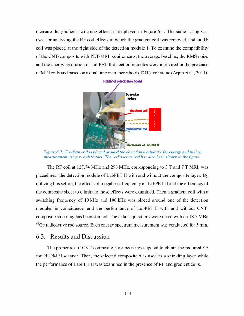
141
measure the gradient switching effects is displayed in Figure 6-1. The same set-up was
used for analyzing the RF coil effects in which the gradient coil was removed, and an RF
coil was placed at the right side of the detection module 1. To examine the compatibility
of the CNT-composite with PET/MRI requirements, the average baseline, the RMS noise
and the energy resolution of LabPET II detection modules were measured in the presence
of MRI coils and based on a dual time over thereshold (TOT) technique (Arpin et al., 2011).
Figure 6-1. Gradient coil is placed around the detection module #1 for energy and timing
measurement using two detectors. The radioactive rad has also been shown in the figure.
The RF coil at 127.74 MHz and 298 MHz, corresponding to 3 T and 7 T MRI, was
placed near the detection module of LabPET II with and without the composite layer. By
utilizing this set-up, the effects of megahertz frequency on LabPET II and the efficiency of
the composite sheet to eliminate those effects were examined. Then a gradient coil with a
switching frequency of 10 kHz and 100 kHz was placed around one of the detection
modules in coincidence, and the performance of LabPET II with and without CNT-
composite shielding has been studied. The data acquisitions were made with an 18.5 MBq
68Ge radioactive rod source. Each energy spectrum measurement was conducted for 5 min.
6.3. Results and Discussion
The properties of CNT-composite have been investigated to obtain the required SE
for PET/MRI scanner. Then, the selected composite was used as a shielding layer while
the performance of LabPET II was examined in the presence of RF and gradient coils.
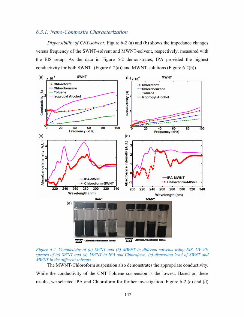
142
6.3.1. Nano-Composite Characterization
Dispersibility of CNT-solvent: Figure 6-2 (a) and (b) shows the impedance changes
versus frequency of the SWNT-solvent and MWNT-solvent, respectively, measured with
the EIS setup. As the data in Figure 6-2 demonstrates, IPA provided the highest
conductivity for both SWNT- (Figure 6-2(a)) and MWNT-solutions (Figure 6-2(b)).
Figure 6-2. Conductivity of (a) SWNT and (b) MWNT in different solvents using EIS. UV-Vis
spectra of (c) SWNT and (d) MWNT in IPA and Chloroform, (e) dispersion level of SWNT and
MWNT in the different solvents.
The MWNT-Chloroform suspension also demonstrates the appropriate conductivity.
While the conductivity of the CNT-Toluene suspension is the lowest. Based on these
results, we selected IPA and Chloroform for further investigation. Figure 6-2 (c) and (d)
(a) (b)
(c) (d)
(e)
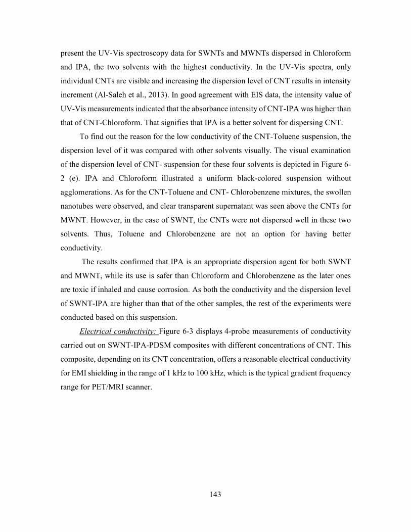
143
present the UV-Vis spectroscopy data for SWNTs and MWNTs dispersed in Chloroform
and IPA, the two solvents with the highest conductivity. In the UV-Vis spectra, only
individual CNTs are visible and increasing the dispersion level of CNT results in intensity
increment (Al-Saleh et al., 2013). In good agreement with EIS data, the intensity value of
UV-Vis measurements indicated that the absorbance intensity of CNT-IPA was higher than
that of CNT-Chloroform. That signifies that IPA is a better solvent for dispersing CNT.
To find out the reason for the low conductivity of the CNT-Toluene suspension, the
dispersion level of it was compared with other solvents visually. The visual examination
of the dispersion level of CNT- suspension for these four solvents is depicted in Figure 6-
2 (e). IPA and Chloroform illustrated a uniform black-colored suspension without
agglomerations. As for the CNT-Toluene and CNT- Chlorobenzene mixtures, the swollen
nanotubes were observed, and clear transparent supernatant was seen above the CNTs for
MWNT. However, in the case of SWNT, the CNTs were not dispersed well in these two
solvents. Thus, Toluene and Chlorobenzene are not an option for having better
conductivity.
The results confirmed that IPA is an appropriate dispersion agent for both SWNT
and MWNT, while its use is safer than Chloroform and Chlorobenzene as the later ones
are toxic if inhaled and cause corrosion. As both the conductivity and the dispersion level
of SWNT-IPA are higher than that of the other samples, the rest of the experiments were
conducted based on this suspension.
Electrical conductivity: Figure 6-3 displays 4-probe measurements of conductivity
carried out on SWNT-IPA-PDSM composites with different concentrations of CNT. This
composite, depending on its CNT concentration, offers a reasonable electrical conductivity
for EMI shielding in the range of 1 kHz to 100 kHz, which is the typical gradient frequency
range for PET/MRI scanner.
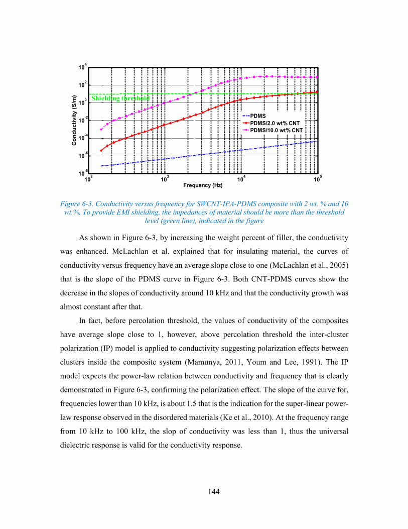
144
Figure 6-3. Conductivity versus frequency for SWCNT-IPA-PDMS composite with 2 wt. % and 10
wt.%. To provide EMI shielding, the impedances of material should be more than the threshold
level (green line), indicated in the figure
As shown in Figure 6-3, by increasing the weight percent of filler, the conductivity
was enhanced. McLachlan et al. explained that for insulating material, the curves of
conductivity versus frequency have an average slope close to one (McLachlan et al., 2005)
that is the slope of the PDMS curve in Figure 6-3. Both CNT-PDMS curves show the
decrease in the slopes of conductivity around 10 kHz and that the conductivity growth was
almost constant after that.
In fact, before percolation threshold, the values of conductivity of the composites
have average slope close to 1, however, above percolation threshold the inter-cluster
polarization (IP) model is applied to conductivity suggesting polarization effects between
clusters inside the composite system (Mamunya, 2011, Youm and Lee, 1991). The IP
model expects the power-law relation between conductivity and frequency that is clearly
demonstrated in Figure 6-3, confirming the polarization effect. The slope of the curve for,
frequencies lower than 10 kHz, is about 1.5 that is the indication for the super-linear power-
law response observed in the disordered materials (Ke et al., 2010). At the frequency range
from 10 kHz to 100 kHz, the slop of conductivity was less than 1, thus the universal
dielectric response is valid for the conductivity response.
102
103
104
105
10-8
10-6
10-4
10-2
100
102
104
Frequency (Hz)
Co
nd
uc
tiv
ity
(S
/m)
PDMS
PDMS/2.0 wt% CNT
PDMS/10.0 wt% CNT
Shielding threshold
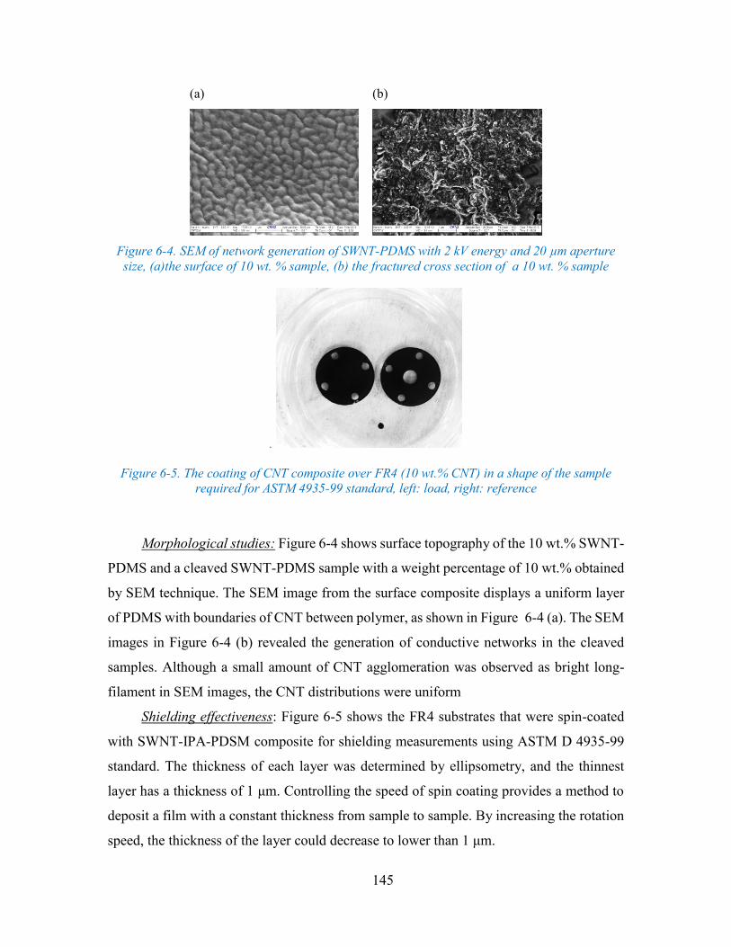
145
(a)
(b)
Figure 6-4. SEM of network generation of SWNT-PDMS with 2 kV energy and 20 µm aperture
size, (a)the surface of 10 wt. % sample, (b) the fractured cross section of a 10 wt. % sample
.
Figure 6-5. The coating of CNT composite over FR4 (10 wt.% CNT) in a shape of the sample
required for ASTM 4935-99 standard, left: load, right: reference
Morphological studies: Figure 6-4 shows surface topography of the 10 wt.% SWNT-
PDMS and a cleaved SWNT-PDMS sample with a weight percentage of 10 wt.% obtained
by SEM technique. The SEM image from the surface composite displays a uniform layer
of PDMS with boundaries of CNT between polymer, as shown in Figure 6-4 (a). The SEM
images in Figure 6-4 (b) revealed the generation of conductive networks in the cleaved
samples. Although a small amount of CNT agglomeration was observed as bright long-
filament in SEM images, the CNT distributions were uniform
Shielding effectiveness: Figure 6-5 shows the FR4 substrates that were spin-coated
with SWNT-IPA-PDSM composite for shielding measurements using ASTM D 4935-99
standard. The thickness of each layer was determined by ellipsometry, and the thinnest
layer has a thickness of 1 μm. Controlling the speed of spin coating provides a method to
deposit a film with a constant thickness from sample to sample. By increasing the rotation
speed, the thickness of the layer could decrease to lower than 1 μm.
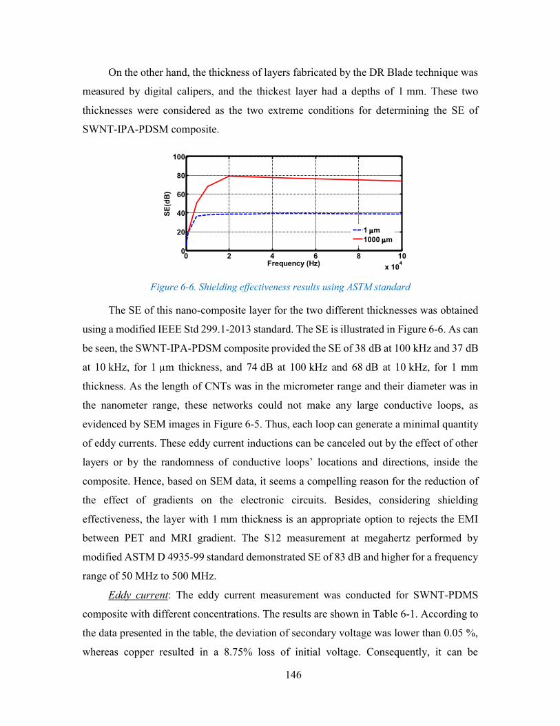
146
On the other hand, the thickness of layers fabricated by the DR Blade technique was
measured by digital calipers, and the thickest layer had a depths of 1 mm. These two
thicknesses were considered as the two extreme conditions for determining the SE of
SWNT-IPA-PDSM composite.
Figure 6-6. Shielding effectiveness results using ASTM standard
The SE of this nano-composite layer for the two different thicknesses was obtained
using a modified IEEE Std 299.1-2013 standard. The SE is illustrated in Figure 6-6. As can
be seen, the SWNT-IPA-PDSM composite provided the SE of 38 dB at 100 kHz and 37 dB
at 10 kHz, for 1 µm thickness, and 74 dB at 100 kHz and 68 dB at 10 kHz, for 1 mm
thickness. As the length of CNTs was in the micrometer range and their diameter was in
the nanometer range, these networks could not make any large conductive loops, as
evidenced by SEM images in Figure 6-5. Thus, each loop can generate a minimal quantity
of eddy currents. These eddy current inductions can be canceled out by the effect of other
layers or by the randomness of conductive loops’ locations and directions, inside the
composite. Hence, based on SEM data, it seems a compelling reason for the reduction of
the effect of gradients on the electronic circuits. Besides, considering shielding
effectiveness, the layer with 1 mm thickness is an appropriate option to rejects the EMI
between PET and MRI gradient. The S12 measurement at megahertz performed by
modified ASTM D 4935-99 standard demonstrated SE of 83 dB and higher for a frequency
range of 50 MHz to 500 MHz.
Eddy current: The eddy current measurement was conducted for SWNT-PDMS
composite with different concentrations. The results are shown in Table 6-1. According to
the data presented in the table, the deviation of secondary voltage was lower than 0.05 %,
whereas copper resulted in a 8.75% loss of initial voltage. Consequently, it can be
0 2 4 6 8 10
x 104
0
20
40
60
80
100
Frequency (Hz)
SE
(dB
)
1 m
1000 m
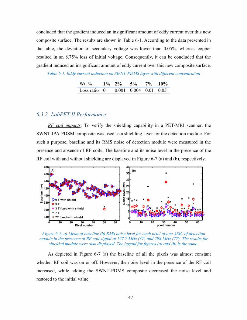
147
concluded that the gradient induced an insignificant amount of eddy current over this new
composite surface. The results are shown in Table 6-1. According to the data presented in
the table, the deviation of secondary voltage was lower than 0.05%, whereas copper
resulted in an 8.75% loss of initial voltage. Consequently, it can be concluded that the
gradient induced an insignificant amount of eddy current over this new composite surface.
Table 6-1. Eddy current induction on SWNT-PDMS layer with different concentration
Wt. % 1% 2% 5% 7% 10%
Loss ratio 0 0.001 0.004 0.01 0.05
6.3.2. LabPET II Performance
RF coil impacts: To verify the shielding capability in a PET/MRI scanner, the
SWNT-IPA-PDSM composite was used as a shielding layer for the detection module. For
such a purpose, baseline and its RMS noise of detection module were measured in the
presence and absence of RF coils. The baseline and its noise level in the presence of the
RF coil with and without shielding are displayed in Figure 6-7 (a) and (b), respectively.
Figure 6-7. a) Mean of baseline (b) RMS noise level for each pixel of one ASIC of detection
module in the presence of RF coil signal at 127.7 MHz (3T) and 298 MHz (7T). The results for
shielded module were also displayed. The legend for figures (a) and (b) is the same.
As depicted in Figure 6-7 (a) the baseline of all the pixels was almost constant
whether RF coil was on or off. However, the noise level in the presence of the RF coil
increased, while adding the SWNT-PDMS composite decreased the noise level and
restored to the initial value.
0 10 20 30 40 50 60
340
360
380
400
420
440
460
480
Pixel number
Ba
se
lin
e (
mv
)
0 T with shield
3 T
3 T fixed with shield
7 T
7T fixed with shield
0 10 20 30 40 50 60
0
5
10
15
20
25
30
35
40
pixel number
No
ise
RM
S (
mv
)
(b)(a)
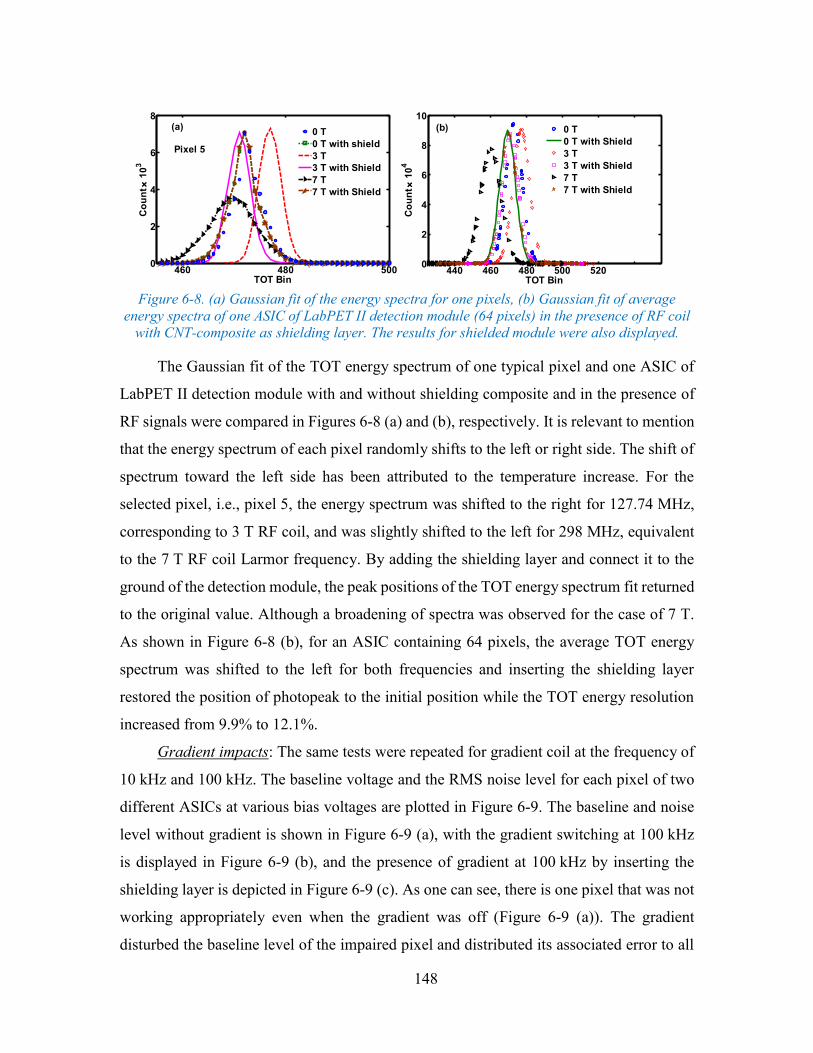
148
Figure 6-8. (a) Gaussian fit of the energy spectra for one pixels, (b) Gaussian fit of average
energy spectra of one ASIC of LabPET II detection module (64 pixels) in the presence of RF coil
with CNT-composite as shielding layer. The results for shielded module were also displayed.
The Gaussian fit of the TOT energy spectrum of one typical pixel and one ASIC of
LabPET II detection module with and without shielding composite and in the presence of
RF signals were compared in Figures 6-8 (a) and (b), respectively. It is relevant to mention
that the energy spectrum of each pixel randomly shifts to the left or right side. The shift of
spectrum toward the left side has been attributed to the temperature increase. For the
selected pixel, i.e., pixel 5, the energy spectrum was shifted to the right for 127.74 MHz,
corresponding to 3 T RF coil, and was slightly shifted to the left for 298 MHz, equivalent
to the 7 T RF coil Larmor frequency. By adding the shielding layer and connect it to the
ground of the detection module, the peak positions of the TOT energy spectrum fit returned
to the original value. Although a broadening of spectra was observed for the case of 7 T.
As shown in Figure 6-8 (b), for an ASIC containing 64 pixels, the average TOT energy
spectrum was shifted to the left for both frequencies and inserting the shielding layer
restored the position of photopeak to the initial position while the TOT energy resolution
increased from 9.9% to 12.1%.
Gradient impacts: The same tests were repeated for gradient coil at the frequency of
10 kHz and 100 kHz. The baseline voltage and the RMS noise level for each pixel of two
different ASICs at various bias voltages are plotted in Figure 6-9. The baseline and noise
level without gradient is shown in Figure 6-9 (a), with the gradient switching at 100 kHz
is displayed in Figure 6-9 (b), and the presence of gradient at 100 kHz by inserting the
shielding layer is depicted in Figure 6-9 (c). As one can see, there is one pixel that was not
working appropriately even when the gradient was off (Figure 6-9 (a)). The gradient
disturbed the baseline level of the impaired pixel and distributed its associated error to all
460 480 5000
2
4
6
8
Pixel 5
TOT Bin
Co
un
t
10
3
0 T
0 T with shield
3 T
3 T with Shield
7 T
7 T with Shield
440 460 480 500 5200
2
4
6
8
10
TOT Bin
Co
un
t
10
4
0 T
0 T with Shield
3 T
3 T with Shield
7 T
7 T with Shield
(a) (b)
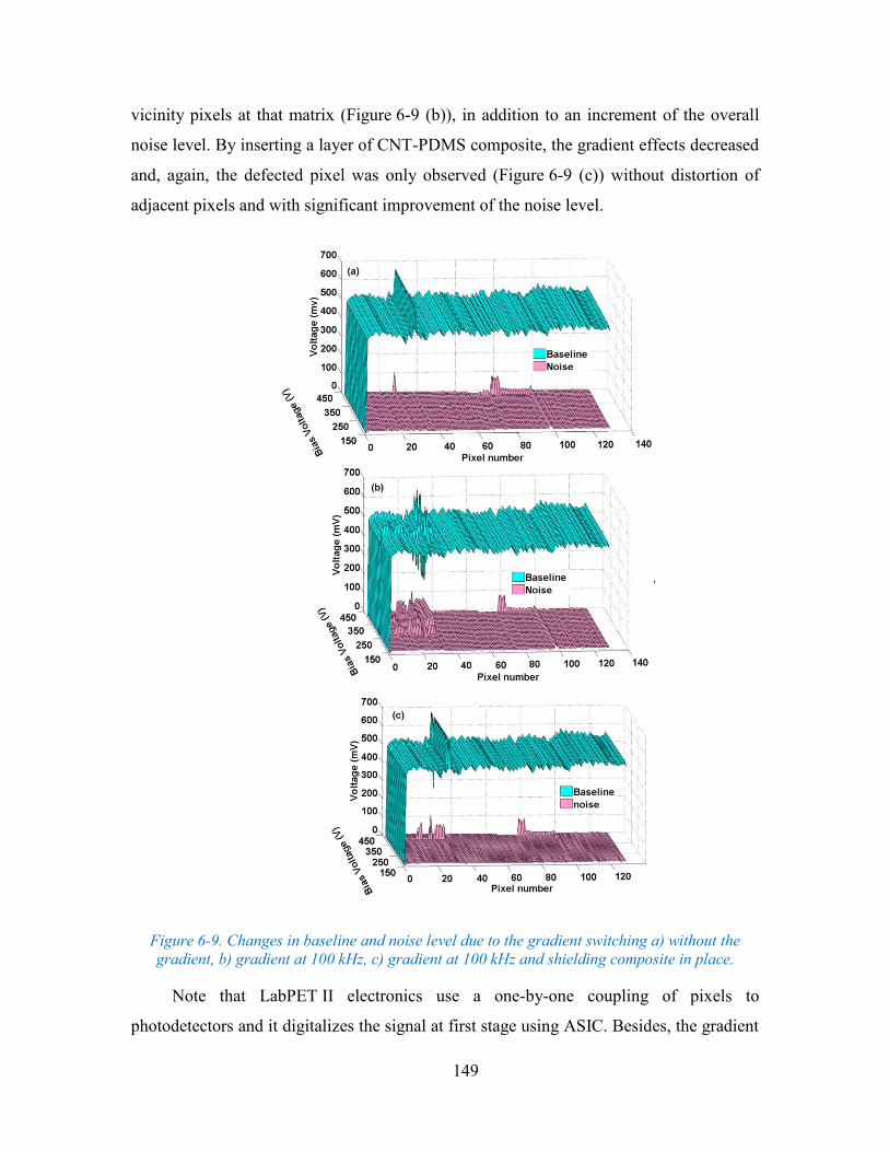
149
vicinity pixels at that matrix (Figure 6-9 (b)), in addition to an increment of the overall
noise level. By inserting a layer of CNT-PDMS composite, the gradient effects decreased
and, again, the defected pixel was only observed (Figure 6-9 (c)) without distortion of
adjacent pixels and with significant improvement of the noise level.
Figure 6-9. Changes in baseline and noise level due to the gradient switching a) without the
gradient, b) gradient at 100 kHz, c) gradient at 100 kHz and shielding composite in place.
Note that LabPET II electronics use a one-by-one coupling of pixels to
photodetectors and it digitalizes the signal at first stage using ASIC. Besides, the gradient
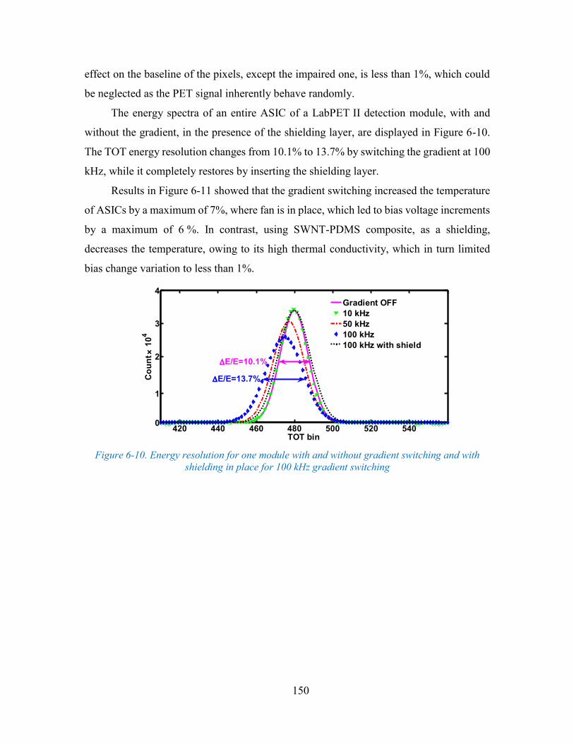
150
effect on the baseline of the pixels, except the impaired one, is less than 1%, which could
be neglected as the PET signal inherently behave randomly.
The energy spectra of an entire ASIC of a LabPET II detection module, with and
without the gradient, in the presence of the shielding layer, are displayed in Figure 6-10.
The TOT energy resolution changes from 10.1% to 13.7% by switching the gradient at 100
kHz, while it completely restores by inserting the shielding layer.
Results in Figure 6-11 showed that the gradient switching increased the temperature
of ASICs by a maximum of 7%, where fan is in place, which led to bias voltage increments
by a maximum of 6 %. In contrast, using SWNT-PDMS composite, as a shielding,
decreases the temperature, owing to its high thermal conductivity, which in turn limited
bias change variation to less than 1%.
Figure 6-10. Energy resolution for one module with and without gradient switching and with
shielding in place for 100 kHz gradient switching
420 440 460 480 500 520 5400
1
2
3
4
TOT bin
Co
un
t
10
4
Gradient OFF
10 kHz
50 kHz
100 kHz
100 kHz with shield
E/E=13.7%
E/E=10.1%
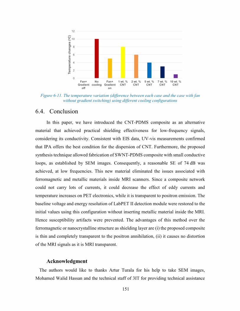
151
Figure 6-11. The temperature variation (difference between each case and the case with fan
without gradient switching) using different cooling configurations
6.4. Conclusion
In this paper, we have introduced the CNT-PDMS composite as an alternative
material that achieved practical shielding effectiveness for low-frequency signals,
considering its conductivity. Consistent with EIS data, UV-vis measurements confirmed
that IPA offers the best condition for the dispersion of CNT. Furthermore, the proposed
synthesis technique allowed fabrication of SWNT-PDMS composite with small conductive
loops, as established by SEM images. Consequently, a reasonable SE of 74 dB was
achieved, at low frequencies. This new material eliminated the issues associated with
ferromagnetic and metallic materials inside MRI scanners. Since a composite network
could not carry lots of currents, it could decrease the effect of eddy currents and
temperature increases on PET electronics, while it is transparent to positron emission. The
baseline voltage and energy resolution of LabPET II detection module were restored to the
initial values using this configuration without inserting metallic material inside the MRI.
Hence susceptibility artifacts were prevented. The advantages of this method over the
ferromagnetic or nanocrystalline structure as shielding layer are (i) the proposed composite
is thin and completely transparent to the positron annihilation, (ii) it causes no distortion
of the MRI signals as it is MRI transparent.
Acknowledgment
The authors would like to thanks Artur Turala for his help to take SEM images,
Mohamed Walid Hassan and the technical staff of 3IT for providing technical assistance
0
2
4
6
8
10
12
Fan+ Gradient
off
No cooling
Fan+ Gradient
on
1 wt. % CNT
2 wt. % CNT
5 wt. % CNT
7 wt. % CNT
10 wt. % CNT
Te
mp
era
ture
ch
an
ges
(oC
)

152
to the project. This work was supported by Fonds de recherche du Québec – Nature et
technologies (FRQNT) and Natural Sciences and Engineering Research Council of Canada
(NSERC) funds.

153
.
154
CHAPTER 7
CONCLUSION
The LabPET II technology was developed at Université de Sherbrooke with the goal
to obtain the best spatial resolution and contrast to noise ratio on PET imaging. Thanks to
the one-to-one coupling of APD to crystal, this configuration provides submillimeter
spatial resolution for small animals and millimeter spatial resolution for the human brain.
In addition, the APD signals are converted to digital signals using ASICs embedded in the
front-end electronics. These two factors produce a less sensitive PET detector to an MRI
environment. This dissertation fulfilled the primary objectives which were to investigate
and to adapt the LabPET II technology in order to realize a PET-insert for MRI scanner.
The works are summarized in four papers including the following contribution to
science. i) The impacts of metallic materials on PET and MRI performance were assessed.
ii) The cross effects of radio-frequency signals between MRI and LabPET II performance,
were investigated. iii) To eliminate the effects of RF and gradient coil pulses on the
LabPET II energy and timing resolution performance, a novel shielding material was
placed between MRI coils and the electronics of the LabPET II. iv) Finally, to enhance the
shielding properties for low-frequency switching gradients, a new composite based on
carbon nanotubes was investigated.
7.1. Summary
An analysis of the different materials of the LabPET detection module, the electronic
part inserted into the MRI FOV, was carried out to satisfy the first objective of this thesis.
The primary objective was to find the inhomogeneity caused by the metallic material of the
detection module. This investigation scrutinizes the inhomogeneity of magnetic fields due
to electronic components to answer that question. Indeed, as a PET detector includes
metallic components, it can interfere with MRI if the material was not selected wisely. Our
results confirm that, when the detection module was placed in the middle of an MRI gantry,
standard connectors containing nickel alter MRI performance as nickel changes the
homogeneity of magnetic fields. However, as the LabPET II detection modules are placed
155
outside the RF coil in the MRI bore, the effect is limited to this specific region. For an MRI
with an open bore diameter of 50 cm, a measurable variation in magnetic field distributions
is observed due to the metallic connector up to 12.5 cm away from the MRI center. Thus
the image from those parts of FOV should be adjusted with a correction factor. The same
effects are detected for ferromagnetic electronic elements of the PET detection modules
with small packaging size of 0201 (0.25 mm 0.125 mm), although the impact was 6-
order of magnitude lower than connectors. By changing the connector to BGA made of
SAC305, a paramagnetic material, this inhomogeneity decreases by 7-order of magnitude.
This statement and the following paragraph answer the second and third objectives of this
thesis in which alternative options were required. Moreover, the displacement effects
(variation of coordinate) with SAC305 decline about 8-order of magnitude in comparison
with nickel-based connectors. Furthermore, our results confirm that increasing the main
magnetic field causes more significant displacement, while lower gradient fields increase
the distortion.
The connectors also add extra problems originating from gradient switching. Results
demonstrate that for higher switching frequencies, both eddy current and heat generation
were intensified. Besides, the magnetic field for the gradient coil switching at a higher rate
shows more variations, causing deviations of the net magnetic field that would ultimately
distort the MR image quality. All these perturbations decrease significantly by using BGA.
Consequently, it is essential to remove the connector from the detection module; the BGA-
based detection module eliminates the issues originating from the different material
susceptibility. In addition, the size of all other electronic components should be decreased
to the smallest available ones.
The fourth objective of the thesis is the investigation of the MR-compatibility of the
LabPET II technology with diverse MRI’s RF and gradient switching conditions. To
realize this objective, two LabPET II detection modules in coincidence along with custom-
made coils mimicking the electromagnetic behaviors of MRI pulses have been used to
examine the LabPET II performance. The RF coil was excited at three different frequencies
of 127.74 MHz, 298 MHz, and 400.25 MHz corresponding to 3 T, 7 T, and 9.4 T MRI.
The gradient coil is switched at 10 kHz, 50 kHz, and 100 kHz. In the presence of each coil,
the performance of LabPET II detection modules, such as their baseline voltage, noise
156
level, energy, and timing resolutions, was assessed to clarify the fourth objective of this
project by identifying the problematic parts of LabPET II detection modules in the presence
of EMI. To attenuate the temperature variations, caused by the gradient switching, a heat
pipe was attached to the back of the electronic board in contact with the ASIC. A shielding
layer of CHO-SHIELD® 2056 paint was placed between the detection module and the coil
to avoide EMIs. The next aim was regarding the properties of the shielding layer; the SE
of the paint layer was measured for different frequencies. It was found to provide SE of
more than 65 dB for a frequency range from 10 kHz to 400 MHz, which is adequate for
PET/MRI applications.
The results without shielding showed that the DDR3 memory of the LabPET II
electronic boards interferes with MRI at 9.4 T. The noise level increment in the presence
of either RF or gradient coils cause a shift to either the left or right in energy photo-peak
and deteriorates the energy and timing resolutions. To eliminate the effect of the DDR3 on
the RF signals, the clock of LabPET II was changed to 106 MHz instead of 100 MHz. As
for the gradient case, first, a heat pipe was added to stabilize the detector module’s
temperature. For higher frequency switching, a degradation of the average timing
resolution and a significant reduction in the signal amplitude were observed, especially for
gradient switching at 50 kHz and 100 kHz. Adding the polymer shielding layer improved
both the energy and timing resolutions of the LabPET II detection module. A shift in the
photopeak was observed after shielding. This effect is a direct consequence of temperature
rise resulting from the confinement of the detection module. As the copper layer employed
by other groups is replaced by a polymer with less conductivity, the eddy current
measurement showed less induced eddy currents on the composite film in comparison to
copper shielding. The obtained results fulfill the main research question and determine
that the LabPET II detection module is compatible with MRI by adding the composite layer
as shielding and using the heat pipe to stabilize the temperature.
Ultimately, the MRI compatibility of a modified LabPET II detection module, named
“interposer detector”, is assessed to answer the request regarding the required
modifications in detector electronic boards from another point of view. The modifications
were implemented based on COMSOL and MATLAB simulation results. The noise level
from RF signals injected to the baseline voltage of the analog shaper is of importance. In
157
the case of the interposer detector, the increment of the noise level is detected for all pixels
of APDs near the RF coil. The energy spectrum of each pixel of the interposer detector was
measured, confirming improvement in TOT energy resolution and decrement in the
photopeak shifts in comparison to the standard detection module. However, to restore the
energy spectrum and eliminate the noise added to the baseline, utilizing a thin layer of
shielding composite or copper was necessary. Albeit, assembling the ASICs between two
boards and using their ground plane as the shielding layer were proposed to exclude EMI,
the level of SE was not enough to eliminate the EMI effects completely and this design
was not able to fulfill its objective.
Finally, to realize the goal concerning CNT composite properties and its fabrication,
a new flexible composite based on CNT and PDMS was synthesized. The impedance of
CNT-solution was measured using an electrochemical impedance analyzer. The
dispersibility of suspensions was assessed through UV-Vis spectroscopy. The structure of
CNT composite with various concentrations of filler was evaluated with SEM. The DC
conductivity of each layer was quantified utilizing the 4-probe method. Lastly, the
shielding effectiveness of the composite films was determined using a modified ASTM-D-
4935-99 standard. Different solvents and mixing methods were examined to improve the
composite characteristic.
Our results confirmed that using IPA as a solvent, and ultra-sonication followed by
shear mixing, provide an excellent homogeneity to reach the highest conductivity at a lower
CNT ratio. Additionally, utilizing IPA reduces the risk of using toxic solvents, such as
chloroform and chlorobenzene. Once the appropriate conductivity for polymer composite
was achieved, this composite was employed to shield the detection modules and measure
the energy and timing resolutions. Measurements showed insignificant induced eddy
currents, and the energy resolution of the shielded module in the presence of the RF and
gradient coils was restored to the LabPET II resolution without EMI.
In summary, the feasibility of modifying the LabPET II detection module to be
compatible with MRI has been demonstrated. The effects of metallic components on MRI
and PET performance were explained comprehensively. It was shown that even inserting
ferromagnetic material outside the MRI field of view causes inhomogeneity of magnetic
fields and distortion of both PET and MRI signals. The performance of the LabPET II
158
detection module was measured to find out the most problematic parts and to investigate
way to overcome those issues. Using commercial composite shielding and heat pipe
improved the LabPET II performance significantly. However, to achieve our ultimate goal,
which is to eliminate eddy current at low frequency, a shielding composite based on CNT
was synthesized. This new strategy shows promising results to recover the LabPET II
performance inside an MRI gantry.
7.2. Discussion
The investigation of the effects of metallic materials located at the periphery of an
MRI bore confirmed that ferromagnetic materials in detection modules cause displacement
artifacts; even though they are situated outside the center of the MRI FOV. For designing
an insert-electronics board, two key factors need to be considered; (i) the conductivity and
(ii) the susceptibility of materials. Removing problematic parts and replacing them with
paramagnetic alloys minimizes the displacement artifacts in MRI images and preserves the
homogeneity of the MRI field. Besides, ferromagnetic material induces a variation in the
gradient magnetic field that impedes the actual gradation of the magnetic field. As for PET
performance, ferromagnetic materials, due to their different susceptibility, generate eddy
current induction and heat in PET electronic components unless minor quantities of metal
are utilized. Therefore, a modified detector, based on BGA technology and electronic
components with the smallest footprint and packaging size, is a viable candidate to resolve
these problems.
The MR-compatibility assessment of the LabPET II detection module reveals that
electromagnetic signals are picked up by the ASIC input; hence, distortion of the signal is
inevitable. Although the energy and timing resolutions got considerably worse, the count
rates remined fairly constant, meaning that there is no data loss. That is a significant
advantage over other PET-insert scanners in which count losses were reported.
Nevertheless, the shielded detection module, using the conductive paint, showed promising
performance in terms of PET performance regarding the energy and timing resolutions.
The required shielding effectiveness was at least 60 dB. With the shielding layer in place,
the temperature rise was observed due to the confinement of the detection modules. The
159
disadvantage of this composite is that it could be broken easily and peeled off from the
surface. Thus a protective layer will be required for long-term usage.
The theoretical results verify the effectiveness of removing connectors and
replacing them with paramagnetic materials. Thus the BGA-based detector, in which the
ASICs were sandwiched between two electronic boards, was supposed to be insensitive to
EMI. In spite of the effort to eliminate EMI with the new design, the results confirmed the
presence of interactions impairing the PET performance. Albeit, compared to the standard
detection module of LabPET II, some enhancement in energy and timing resolutions was
observed. In addition, this new design used the embedded thermal pads to extract the heat
properly, thus the shift in the photopeak was not significant for the interposer detectorin
the presence of EMIs. Our results confirmed that the noise enters the electronics of
LabPET II from both sides of the detection module PCBs. Thus, placing a mesh-structured
ground at each top-level of PCB, instead of a buried layer inside the PCB, was proposed to
realize a PET-insert that performs in high electromagnetic fields without demanding a
shielding configuration.
The CNT-based composite was selected to overcome the deficiencies of the other
suggested shielding materials since they were inadequate to prevent eddy current induction
and hence, caused heat, vibrations, and gradient field changes. The difference between
carbon fibre and CNT composite comes from the unique properties of CNT. Indeed, CNTs
have a higher aspect ratio than carbon fibres; consequently, it is plausible to reach sufficient
electrical conductivity to shield both gradient coil and RF coil pulses. Whereas, the
shielding layer based on carbon fibre was unable to remove low-frequency interferences
and inserting a copper layer was required, which invokes the eddy current induction. A
copper layer provides a large conductive loop and acts as a free electron sea while the
composite structure is composed of very small loops. Because of this feature, the miniature-
sized eddy current loops generated in the composite; thus in general, the effects of eddy
current inductions become insignificant.
Employing carbon nanotubes-based composites to enhance the performance of
telecommunication systems in space applications proves the ability of such a composite to
shield EMI. However, the prerequisite SE of those applications is lower than that of the
PET-insert. The major shielding effectiveness investigations of CNT-based composite
160
were in the Gigahertz frequency range and little work was reported in the Megahertz range.
However, there were not results for the kHz range that were of interest for gradient
switching. The highest SE acquired by CNT-based composite was reported as 47 dB at
10 MHz frequency (Li et al., 2006), with a long single-walled carbon nanotube. Whereas,
the PET/MRI scanner requires at least 60 dB of shielding effectiveness.
Fabricating CNT-based composite with high conductivity to reach a SE of 60 dB
necessitates extraordinary homogeneity of samples. Different mixing methods were
examined to realize a suitable dispersion level. In the composite fabrication process using
solvents, it is essential to select a mixing technique that supplies energy higher than the
binding energy of the aggregation of CNT and lower than the necessary amount to fracture
a CNT. Theoretically, the energy density required to separate a pair of SWNT is 100 MPa,
while for an MWNT this energy decreases to about 16 kPa. Moreover, the energy from
shear stress is below 20 kPa. Hence, shear mixing alone is not a suitable technique for high-
level dispersion of SWNT clusters. The ultra-sonication method provided a 100 MPa shear
stress that is enough to overcome the binding energy of SWNTs.
The new CNT composite was fabricated by combining ultra-sonication and shear
mixing methods to reach an excellent homogeneity and increase its conductivity at a
frequency range from 10 kHz to 500 MHz. A 1-mm thick composite layer is produced
using the DR Blade technique. The CNT composites with different concentrations of filler
were characterized to obtain the essential properties for the PET/MRI application. The
results support that CNT-IPA-PDMS composite with 10 wt.% is a viable candidate as a
shielding layer. This layer offers adequate shielding effectiveness with an insignificant
amount of eddy currents. Shielding the LabPET II detection module with CNT composite
provides a practical option to realize a PET-insert based on the LabPET II technology. This
module could be inserted inside any MRI, with a magnetic field of 3 T to 9.4 T, without
electromagnetic interaction while the eddy current inductions over the shielding layer are
compensated. Note that, the shielding layer would also be capable of removing the EMIs
of other clinical magnetic field MRIs such as 1.5 T magnetic field or lower.
161
7.3. Contribution
Investigation in the medical imaging domain and detection of malignant tissues is
benefiting from a simultaneous PET/MRI scanner. This scanner provides both anatomical
and physiological information to facilitate the diagnosis and analysis of studied objects.
However, the electromagnetic interactions between the two modalities impose several
challenges. Apart from the ideas that support changing the MRI gantry to allow inserting
PET detectors, the most common method to overcome the EMI is to use an appropriate
shielding layer. Copper and carbon fibre were two proposed materials in this regard.
Nonetheless, these materials are still prone to generate eddy current effects. In this project,
the MR-compatibility of LabPET II was scrutinized. In this context, the presented work
includes four essential elements demonstrated in chapters 3 to 6.
The idea is that even a metallic component inserted between the gradient and RF
coils could cause displacement artifacts and generate heat and eddy currents. To
accomplish this objective, the effects of the metallic material of LabPET II detection
modules on the MRI and PET performance, especially the homogeneity of the magnetic
field, were examined in chapter 3. The theoretical investigations using MATLAB code and
COMSOL simulations were carried out to determine the spatial distortion or eddy current
artifacts due to metallic materials of PET detection modules. It is the first time that metallic
material behaviors were surveyed outside the center of MRI FOV. Previous works on MRI
susceptibility to metal were performed on the metallic implants inserted inside the MRI to
acquire the images (Shafiei et al., 2003, Costa et al., 2009); however, in the case of
PET/MRI, the electronic parts of PET are inserted at a distance from the center. The
obtained results confirmed the assumption that the ferromagnetic materials of a PET-insert
at 25 cm away from the center of FOV provokes the inhomogeneity in the magnetic field
that causes variation in the gradient field and induces heat and eddy currents on the
conductive layer.
Chapter 4 summarizes the EMI effects on the LabPET II detection modules. To our
knowledge, it is the first time that the performance of LabPET II detection module has been
studied systematically in the presence of EMIs from MRI signals. Since LabPET II
technology digitizes signals in ASICs embedded in its front-end electronics, it is bound to
162
be less susceptible to EMI. Besides, it employs a one-to-one coupling of crystal to APD
and uses the time-over-threshold method to acquire the data. The other works on PET/MRI
were based on SiPMs (Schulz et al., 2009) or position-sensitive APDs (Caldeira et al.,
2018) that make them much more sensitive to spatial distortion, since these configurations
have used light-sharing schemes. To have more freedom in this thesis, stand-alone RF coils
and gradient coil were devised. For that purpose, three hexagonal coils were designed with
a center frequency at Larmor frequency of 3 T, 7 T, and 9.4 T MRI used to mimic the
behavior of the RF coil of MRI. Besides, a small coil and an alternating current source,
with 45 W power driving that coil, are developed to switch at a frequency range of 10 kHz-
100 kHz and to act as the gradient coil with a slew rate of ~ 200 T/m/s.
The next step explained in chapter 4 is to examine a shielded LabPET II detection
module and observe its performance to verify the effectiveness of this method. Copper and
carbon fiber, used in commercial and research-based PET/MRI scanners, were susceptible
to eddy current inductions or low shielding effectiveness, respectively (Kang et al., 2009,
Peng et al., 2014a). This thesis claims that conductive polymer could eliminate mutual
EMIs between PET and MRI with excellent SE and little eddy current inductions. For
shielding the RF coil signals, a layer of conductive paint deposited over an FR4 sheet as
the substrate is used. This scheme is valid for a surface hexagonal coil. As for shielding the
gradient switching pulses, two different shielding configurations are considered. In the first
arrangement, inside the gradient coil is covered by a composite layer. By utilizing this
technique, the noise injection decreases by one half. However, it is still enough to impede
PET performance. In the second configuration, the detection module and voltage regulators
are wrapped in a layer of the composite. This process offers rejection of noise by about
90% and restoration of LabPET II performance. Therefore, achieved results confirm that a
layer of CHO-SHIELD® 2056 paint with high conductivity is an excellent option for
PET/MRI application since it offers SE of more than 65 dB and it causes less eddy current
inductions.
Chapter 5 describes the performance of a modified LabPET II detection module in
which the connectors were replaced by BGA connections, and the ASICs were sandwiched
between two PCB layers. This design was accomplished at the GRAMS group. The goal
of this thesis was to find out whether the new configuration could enhance LabPET II
163
performance in the presence of EMI or not. The results clarify that the usage of a BGA-
based detection module, based on an “interposer detector”, reduces the interactions
between PET and MRI; however, the interposer still needs to be shielded to perform
appropriately. Thus, a modification is proposed in which the ground layers of the PCB have
to move to the top and bottom layers for better shielding. Such an adjustment will preserve
the LabPET II performance while the electronics of PET will emit fewer electromagnetic
fields.
Chapter 6 covers the fabrication and utilization of CNT-composite for PET/MRI
applications. A new composite based on CNT is suggested. The assumption was that CNT-
based composite provides an appropriate level of SE for communication application, thus
by improving its properties, it would be plausible to use it for a PET/MRI scanner. To
have homogeneous samples, the level of dispersion of CNT in the solvent is a critical
parameter. Hence, different solvents were explored to identify an appropriate solution
regarding the dispersion of CNT. Several fabrication methods were examined to obtain the
required conductivity for shielding EMIs in a simultaneous PET/MRI. Generally, shear
mixing (Huang et al., 2006) or ultrasonication bath (Kim et al., 2018) is used to synthesize
a composite. However, in this thesis, a combination of both shear mixing and ultra-
sonication was used to overcome the binding energy while preventing more fractures. The
ultra-sonication is employed to mix SWNT with a solvent. As the high-level dispersion of
CNT was established through sonication, the polymer mixture is accomplished by a shear
mixing method. Afterward, the CNT-composite layer, with appropriate characteristics, is
used to shield a detection module under EMI and discover the performance of a shielded
module. The results confirm that by selecting a suitable solvent to reach a high level of
dispersion and by controlling the synthesizing process, the EMI shielding of PET/MRI
using CNT-PDMS composite is feasible.
Additionally, in chapters 4 and 6, instead of inserting different shielding materials
inside the MRI bore to identify the chemical shift error as the indication of eddy current, a
new set-up was devised. A set-up including two equal coils is designed to examine the
eddy current inductions over each conductive layer. The allegation was that a composite
layer could remove eddy current effects while providing adequate SE. Our results confirm
that the eddy current effects from copper-silver composite are 12 times less than the copper
164
sheet. As for CNT composite, the loss of signal is insignificant for different weight
percentages (1% to 10%) of the CNT filler. Both composites offer SE of more than 60 dB.
7.4. Future work
By considering the aspects covered in this thesis, some important future work could
be highlighted as follows:
The first work is inserting the shielded LabPET II detection module inside a 3 T MRI
and measuring the performance of MRI while the LabPET II is not working. Then, the
LabPET II detection module can be powered on, and the LabPET II and MRI performance
can be evaluated. If acceptable results are acquired, afterward, a phantom image obtained
with a complete scanner could confirm the spatial resolution superiority of LabPET II over
the other competitors.
The second aspect is fabricating CNT composite with functionalized CNT. In fact,
CNTs with a functional group provide better dispersion in solvents; thus, the composite
filled by a functionalized CNT could deliver higher conductivity. The effects of different
agents, for instance, a hydroxyl group or carboxyl group, could be examined. A solvent,
based on the functionalized agent properties, should be selected and the conductivity of the
new composite has to be measured.
The subsequent task is to improve the shielding effectiveness at high frequency with
a lower concentration of CNT. For that purpose, a mixture of MWNT and SWMT as a
filler is a logical option. Indeed, the MWNT-based composites show higher SE than
SWNT-based composites for frequencies in the megahertz range. In this project, the main
objective was to compensate for the eddy current inductions, which is achieved with
SWNT-based composite. However, obtaining similar results with MWNT/SWNT-based
composite is a practical method to reduce the total cost of shielding.
In addition to excellent electrical conductivity, CNT-composites provide reasonable
thermal conductivity. Thus a CNT-composite could be employed to improve the heat
dissipation. Here, the thermal performance of the CNT-composite was not studied,
although it has an outstanding potential to be used for the LabPET II detection module
instead of using heat pipes.
165
To exclude the EMI effects, it is worth to improve the filter circuit and increase the
bandpass of front-end electronics. Enhancing the power supply rejection ratio (PSSR) of
the filter circuit and using a high-frequency amplifier provides an opportunity to eliminate
the additional noise at the input of detection modules and reject all the noise originating
from the MRI Larmor frequency. In fact, the performance of LabPET II and simulation of
PSSR for pixels with high leakage current confirm that the LabPET II front-end electronic
must be redesigned to reject the noise in the required bandwidth. Furthermore, employing
a specified filter with appropriate PSSR could remove the necessity to have a shielding
configuration.
Last but not least, instead of adding heat pipe outside the ASICs, one could design
an ASIC with an embedded heat pipe inside its substrate. The advantage of such a design
is the realization of a compact structure with constant behavior. As the heat pipe will be
fabricated for our specific requirement, we could regulate the detection module
temperature by controlling the fabrication process.
Finally, the influences of metallic material on the MRI and the electronics boards
inserted inside the MRI are valid for other applications such as designing a thermometer to
monitor the temperature of the patients inside an MRI. Based on the presented data, for any
electronic boards or materials that require installation near or in the presence of an
electromagnetic field, the requirement is clear. Even for paramagnetic materials, the use of
a highly conductive layer with different susceptibility than air causes artifacts in the MRI
and distortion of PET performance.
Besides, the PET-insert based-on LabPET II detector technology opens a new trend
in the PET/MRI scanner. Since the new shielding configuration is flexible, light-weighted,
and easy to process, it could be used instead of the standard shielding layers. In addition,
as the LabPET II detection module digitizes the data at the first electronic level, it requires
less adjustment compared to other counterparts. A PET-insert shielded by CNT-composite
is not susceptible to eddy current inductions. By eliminating the eddy currents and
associated temperature variations, the APD array is more likely to perform at its full
capacity. Besides, the chemical shift errors of MRI due to shielding material susceptibility
and conductivity are excluded. Thus, a PET/MRI acquisition with fast switching
sequences, such as echo-planar imaging (EPI) could be achieved. This sequence acquires
166
individual MRI slices in msec time frame, accordingly minimizing the effects of patient
movements. Previous works reported in the literature were unable to eliminate the eddy
current artifacts and acquire the EPI mode.
Moreover, the conventional methods for the attenuation correction in PET/MRI
utilize the attenuation map that is extracted based on the anatomical data. However, these
data are variable in patients. Thus, a technique based on MR image contrast is preferable.
This goal could be completed by executing an ultra-short echo time sequence. Nonetheless,
carrying out a sequence with microsecond echo-time is impossible in the presence of a
metallic shielding. While using the proposed shielding for the LabPET II detection
module, it is possible to correct the attenuation with image contrast instead of template-
based and segmentation-based methods.
7.5. French conclusion
Les scanners TEP/IRM simultanés offrent une occasion unique d'examiner en même
temps les propriétés anatomiques et fonctionnelles des tissus pathologiques, tout en évitant
l'incertitude du système séquentiel de TEP/IRM. Cependant, le couplage
électromagnétique entre les deux modalités constitue un défi important à traiter. Ces
interférences électromagnétiques entravent les performances du scanner et altèrent la
qualité d'image de chaque modalité.
La technologie LabPET II a été développée à l’Université de Sherbrooke dans le but
d’obtenir la meilleure résolution spatiale et le meilleur rapport contraste/bruit dans des
images TEP. Grâce au couplage un à un des photodiodes à avalanches (PDA) aux cristaux,
cette configuration offre une résolution spatiale submillimétrique pour les petits animaux
et une résolution spatiale millimétrique pour le cerveau humain. L'électronique LabPET II
comprend des circuits intégrés à application spécifique dans lesquels le signal est numérisé
à proximité de la photodiode à avalanche et offre un environnement moins sensible aux
interférences électromagnétiques. Les résultats de cette thèse répondent à l’objectif
principal qui était d’adapter la technologie LabPET II afin de réaliser un insert TEP pour
IRM.
167
Bien que les métaux possèdent d'excellentes propriétés de blindage contre les
radiofréquences, ils ne constituent pas nécessairement une option de blindage appropriée
pour modifier les champs magnétiques induisant des courants de Foucault dans les couches
métalliques. Alors, il existe une demande considérable pour un nouveau matériau de
protection et une approche originale pour retirer les pièces métalliques du champ de vue
de l’IRM.
L’objectif de ce projet était d’initier la réalisation d’un scanner TEP/IRM simultané
basé sur des modules de détection LabPET II. Pour atteindre l'objectif principal,
premièrement, l'effet des matériaux métalliques des modules de détection LabPET II sur
les performances de la TEP et de l'IRM a été examiné théoriquement. Les résultats
confirment que les composants métalliques du module de détection LabPET II influencent
le champ magnétique, génèrent des courants de Foucault qui augmentent la température.
Ensuite, les performances électroniques des modules de détection LabPET II sous
l’influence de bobines d’IRM faites sur mesure ont été examinées. Les résolutions en
énergie et temporelle se détériorent en présence de bobines RF et de bobine à gradient en
raison des perturbations électromagnétiques. Subséquemment, un module de détection
LabPET II blindé par une fine couche de composite cuivre-argent a été étudié, prouvant
que le blindage contre les interférences électromagnétiques avec le composite rétablit les
performances en TEP, tout en générant moins d'induction par courants de Foucault. En
outre, une nouvelle configuration de blindage basée sur une couche flexible d'un composite
de nanotubes de carbone a été fabriquée pour limiter les interférences électromagnétiques.
Les composites de nanotubes de carbone créent une couche hautement conductrice avec
des chemins conducteurs minimaux, ce qui permet de réduire les courants de Foucault.
En résumé, l'insertion d'un module de détection de TEP dans le champ de vue d'un
IRM pose des problèmes en raison du comportement du métal dans un champ magnétique
puissant. Cet aspect a été traité au chapitre 3. Les matériaux métalliques placés hors du
champ de vision de l'IRM pourraient quand même perturber les performances de l'IRM,
mais aussi augmenter la température et les vibrations, entraînant une faiblesse prématurée
de l'électronique TEP. Pour étudier la compatibilité du module de détection LabPET II à
l’intérieur de tube IRM, on présente une étude théorique des artefacts induits par les métaux
provenant de matériaux présents dans le module de détection LabPET II. En outre, les
168
effets des courants de Foucault et la perte de chaleur associée sur le module de détection
TEP, ont été examinés à l’aide de simulations COMSOL. Les résultats montrent qu'en
utilisant un module de détection LabPET II modifié, l'artefact de déplacement (distorsion
de l'image IRM) provenant de l'introduction de petites quantités de métal non
ferromagnétique et les effets thermiques du métal en raison de la commutation de gradient
ont été respectivement réduits de 4 ordres de grandeur pour l'IRM et la TEP. Les effets de
la commutation du gradient de l'IRM sur le module de détection LabPET II ont également
été étudiés et ont révélé que les matériaux métalliques dont la sensibilité est différente de
celle de l'air peuvent provoquer l'induction des courants de Foucault et la dissipation de la
chaleur à moins que on l’utilise de petites quantités avec des distributions éparses. Donc,
le module de détection LabPET II, avec quelques ajustements mineurs, serait compatible
avec l'IRM pour fonctionner efficacement en périphérie du champ de vue d'IRM sans
perturber ses performances.
D'un autre côté, au chapitre 4, nous étudions la compatibilité du module de détection
LabPET II avec l’IRM dans le but de développer un système TEP/IRM simultané. Le
dispositif expérimental évalue les performances de deux modules de détection LabPET II
à proximité d'une bobine RF excitée à trois fréquences différentes imitant les
comportements électromagnétiques des scanners IRM de 3 T, 7 T et 9,4 T. Une bobine à
gradient, avec une fréquence de commutation de 10 kHz à 100 kHz, entoure également l'un
des modules de détection afin de déterminer les effets du gradient du champ magnétique
sur les performances du module de détection, telles que le niveau de référence et le niveau
de bruit, ainsi que les résolutions en énergie et temporelle. Les mesures démontrent un
décalage de la position du pic d'énergie (≤ 9%). Les interférences électromagnétiques
entraînent une dégradation moyenne d'environ 60% de la résolution en énergie TOT et
d'environ 26% de la résolution temporelle. À partir de ces résultats, une version modifiée
du module de détection, comprenant un blindage composite ainsi qu'un mécanisme de
refroidissement amélioré basé sur un caloduc, capable de stabiliser la température du
module de détection à 40 ° C, a été proposée et testée. En utilisant la peinture CHO-
SHIELD® 2056 comme couche de blindage EMI, non seulement les effets des
interférences électromagnétiques de la bobine RF et de la commutation de gradient ont été
compensés, mais les courants de Foucault ont également été réduits en raison de la
169
conductivité inférieure du matériau du blindage. De plus, en stabilisant la température à
l'aide de caloducs, les effets indésirables des variations de gain des photodiodes en raison
des changements de température ont été éliminés. Cette version modifiée ne présentait
aucun signe de dégradation des performances dans un environnement IRM. Les résultats
expérimentaux ont montré que la version modifiée du module de détection LabPET II
constituerait un bon candidat en tant que module de détection pour un scanner TEP
compatible avec la technologie IRM.
Cependant, la faisabilité d'une telle bi-modalité est limitée par la grande taille radiale
du module de détection ainsi que par les composants contenant des matériaux
ferromagnétiques. Donc, au chapitre 5, nous étudions une nouvelle électronique frontale
basée sur l’architecture LabPET II, appelée « détecteur interposeur ». Les performances du
détecteur interposeur en présence de signaux RF et d'impulsions de bobine à gradient y
sont examinées. Les résultats montrent que du bruit a été injecté au niveau de à la carte
électronique. Bien que la nouvelle architecture ait été conçue pour rendre le module de
détection immunisé contre les EMI, de chaque côté de la carte PCB, la couche supérieure
est restée sans protection EMI. Par conséquent, les signaux de ces couches ont été déformés
par des impulsions IRM. Le détecteur interposeur offre toutefois des performances
thermiques supérieures; par conséquent, les effets des variations de température sur les
performances du détecteur interposeur étaient moins importants que ceux du module de
détection standard. Le changement moyen de résolution en énergie diminue quatre fois et
le niveau de bruit moyen de la tension de base diminue de deux ordres de grandeur par
rapport au module de détection standard. Pour les signaux RF et la commutation de
gradient, la peinture CHO-SHIELD® 2056, en tant que couche de blindage EMI, a été
capable d'éliminer les effets EMI sur les performances du détecteur interposeur, dont le
concept repose sur la technologie LabPET II. Pour améliorer encore les performances
interposeur, il est suggéré d'ajouter des plans de masse sur les deux faces externes du
circuit, ce qui augmente les coûts liés à la fabrication de nouvelles cartes. Par conséquent,
il va de soi que le développement d'une couche de blindage est plus attractif, tant sur le
plan commercial que technique, par rapport à révision complète de la conception.
Enfin, les nanotubes de carbone ont montré des propriétés prometteuses en tant que
matériau de remplissage pour augmenter la conductivité électrique des composites. Il a été
170
utilisé pour la fabrication de composites de blindage à haute fréquence, mais ses propriétés
à basse fréquence demeurent encore peu connues. Au chapitre 6, la fabrication du nouveau
composite à base de polydiméthylsiloxane (PDMS) et de nanotubes de carbone (CNT) a
été présentée pour éliminer l’impact des interférences électromagnétiques à basse
fréquence sur les scanners de TEP/IRM. Pour fabriquer une solution composite homogène,
nous avons combiné les méthodes d’ultra-sonication et de mélange à cisaillement.
Conformément aux données de l'EIS, les mesures UV-vis ont confirmé que l'IPA offre les
meilleures conditions pour la dispersion des CNT. De plus, la technique de synthèse
proposée a permis la fabrication d'un composite SWNT-PDMS avec de petites boucles
conductrices, tel qu'établi par les images SEM. En outre, la mesure de l'impédance a
confirmé qu'un composite produit avec ce procédé de traitement fournit la conductivité
requise pour le blindage contre les interférences électromagnétiques dans la plage de
fréquences souhaitée. Par conséquent, une efficacité de blindage raisonnable de 74 dB a
été atteinte, à basse fréquence. Ce nouveau matériau a éliminé les problèmes associés aux
matériaux ferromagnétiques et métalliques à l'intérieur des scanners IRM. Les résultats de
la performance des détecteurs TEP montrent qu’en utilisant ce composite, les défauts liés
au gradient de l’IRM sont compensés pour les performances des modules de détection
LabPET II, tel que démontré en mesurant la résolution en énergie et temporelle.
En examinant les aspects couverts dans cette thèse, certains travaux futurs
importants pourraient être soulignés comme suit :
Le premier travail consisterait à insérer le module de détection LabPET II blindé à
l'intérieur d'un IRM de 3 T et à mesurer la performance de l'IRM lorsque le LabPET II ne
fonctionne pas. Ensuite, le module de détection LabPET II pourrait être mis sous tension
et les performances du LabPET II et de l'IRM pourraient de nouveau être évaluées. Si les
résultats acceptables sont obtenus par la suite, une image de mire à l'aide d'un scanner TEP
complet insérédans l'IRM pourrait confirmer la supériorité de la résolution spatiale de
LabPET II sur les autres concurrents.
Le deuxième aspect est la fabrication d'un composite avec des CNT fonctionnalisés.
En fait, les CNT avec groupe fonctionnel assurent une meilleure dispersion dans les
solvants ; ainsi, le composite rempli par des CNT fonctionnalisés fournirait une
conductivité plus élevée. Les effets de différents agents, par exemple, un groupe hydroxyle
171
ou un groupe carboxyle, pourraient être examinés. Un solvant, basé sur les propriétés de
l'agent fonctionnalisé, doit être choisi et la conductivité du nouveau composite doit être
mesurée.
En plus d'une excellente conductivité électrique, les composites de CNT offrent une
conductivité thermique raisonnable. Ainsi, un composite de CNT pourrait être utilisé pour
améliorer la dissipation de la chaleur. La performance thermique du composite de CNT n'a
pas été complètement étudiée dans cette thèse, bien qu'il ait un potentiel exceptionnel pour
être utilisé pour le module de détection LabPET II au lieu d'utiliser des caloducs.
Pour exclure les effets EMI, il est important d'améliorer le circuit de filtrage et
d'augmenter la bande passante de l'électronique frontale. L'amélioration du circuit de
filtrage et l'utilisation d'un amplificateur haute fréquence permet d'éliminer le bruit
supplémentaire à l'entrée des modules de détection et de rejeter tout le bruit provenant de
la fréquence de Larmor des IRM.
Enfin, au lieu d'ajouter un caloduc à l'extérieur des ASICs, on pourrait concevoir un
ASIC avec un caloduc intégré dans son substrat. L'avantage d'une telle conception est la
réalisation d'une structure compacte avec un comportement constant. Comme le caloduc
serait fabriqué en fonction de nos besoins spécifiques, la température du module de
détection pourrait être mieux régulée en contrôlant le processus de fabrication.
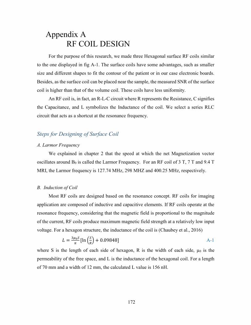
172
Appendix A
RF COIL DESIGN
For the purpose of this research, we made three Hexagonal surface RF coils similar
to the one displayed in fig A-1. The surface coils have some advantages, such as smaller
size and different shapes to fit the contour of the patient or in our case electronic boards.
Besides, as the surface coil can be placed near the sample, the measured SNR of the surface
coil is higher than that of the volume coil. These coils have less uniformity.
An RF coil is, in fact, an R-L-C circuit where R represents the Resistance, C signifies
the Capacitance, and L symbolizes the Inductance of the coil. We select a series RLC
circuit that acts as a shortcut at the resonance frequency.
Steps for Designing of Surface Coil
A. Larmor Frequency
We explained in chapter 2 that the speed at which the net Magnetization vector
oscillates around B0 is called the Larmor Frequency. For an RF coil of 3 T, 7 T and 9.4 T
MRI, the Larmor frequency is 127.74 MHz, 298 MHZ and 400.25 MHz, respectively.
B. Induction of Coil
Most RF coils are designed based on the resonance concept. RF coils for imaging
application are composed of inductive and capacitive elements. If RF coils operate at the
resonance frequency, considering that the magnetic field is proportional to the magnitude
of the current, RF coils produce maximum magnetic field strength at a relatively low input
voltage. For a hexagon structure, the inductance of the coil is (Chaubey et al., 2016)
𝐿 =3𝜇0𝑆
𝜋[ln (
𝑆
𝑅) + 0.09848] A-1
where S is the length of each side of hexagon, R is the width of each side, µ0 is the
permeability of the free space, and L is the inductance of the hexagonal coil. For a length
of 70 mm and a width of 12 mm, the calculated L value is 156 nH.
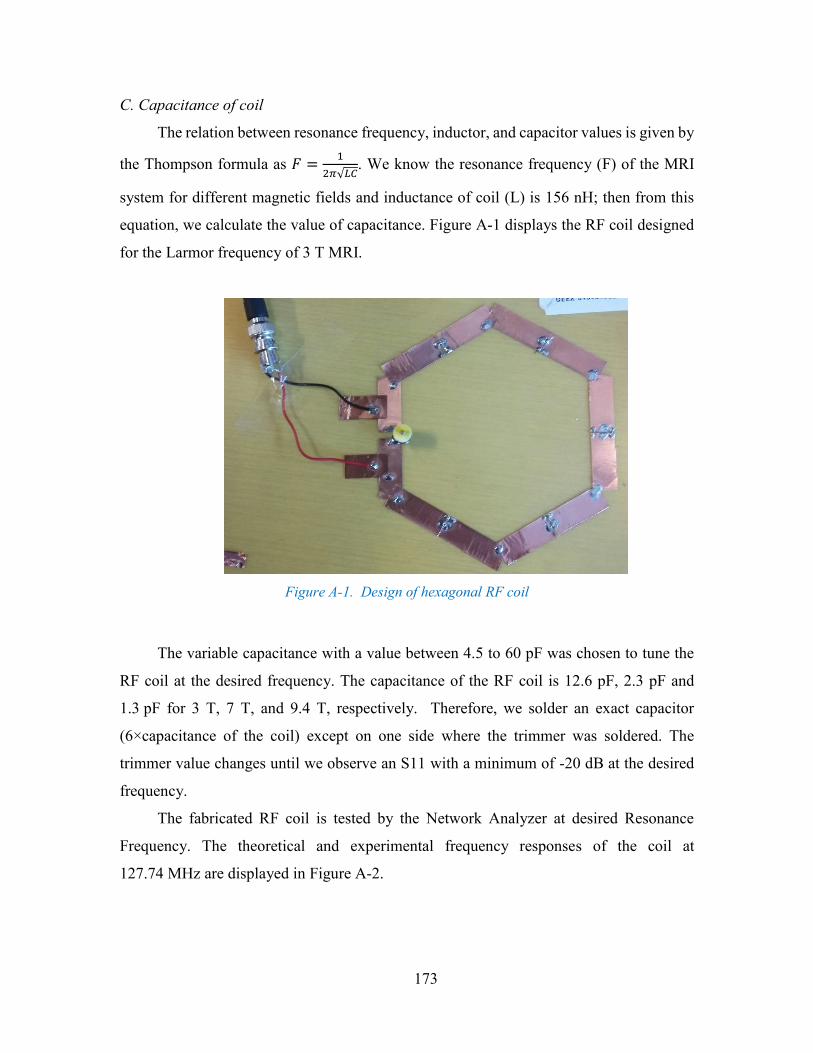
173
C. Capacitance of coil
The relation between resonance frequency, inductor, and capacitor values is given by
the Thompson formula as 𝐹 =1
2𝜋√𝐿𝐶. We know the resonance frequency (F) of the MRI
system for different magnetic fields and inductance of coil (L) is 156 nH; then from this
equation, we calculate the value of capacitance. Figure A-1 displays the RF coil designed
for the Larmor frequency of 3 T MRI.
Figure A-1. Design of hexagonal RF coil
The variable capacitance with a value between 4.5 to 60 pF was chosen to tune the
RF coil at the desired frequency. The capacitance of the RF coil is 12.6 pF, 2.3 pF and
1.3 pF for 3 T, 7 T, and 9.4 T, respectively. Therefore, we solder an exact capacitor
(6×capacitance of the coil) except on one side where the trimmer was soldered. The
trimmer value changes until we observe an S11 with a minimum of -20 dB at the desired
frequency.
The fabricated RF coil is tested by the Network Analyzer at desired Resonance
Frequency. The theoretical and experimental frequency responses of the coil at
127.74 MHz are displayed in Figure A-2.
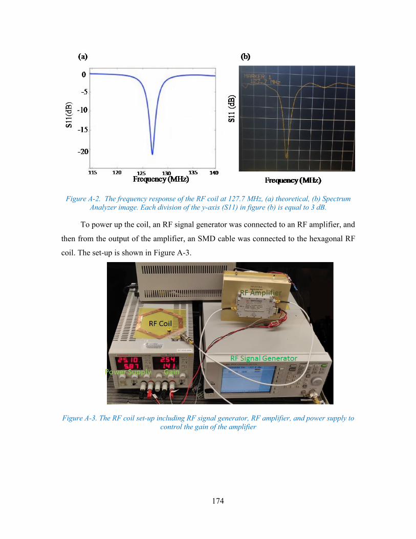
174
Figure A-2. The frequency response of the RF coil at 127.7 MHz, (a) theoretical, (b) Spectrum
Analyzer image. Each division of the y-axis (S11) in figure (b) is equal to 3 dB.
To power up the coil, an RF signal generator was connected to an RF amplifier, and
then from the output of the amplifier, an SMD cable was connected to the hexagonal RF
coil. The set-up is shown in Figure A-3.
Figure A-3. The RF coil set-up including RF signal generator, RF amplifier, and power supply to
control the gain of the amplifier
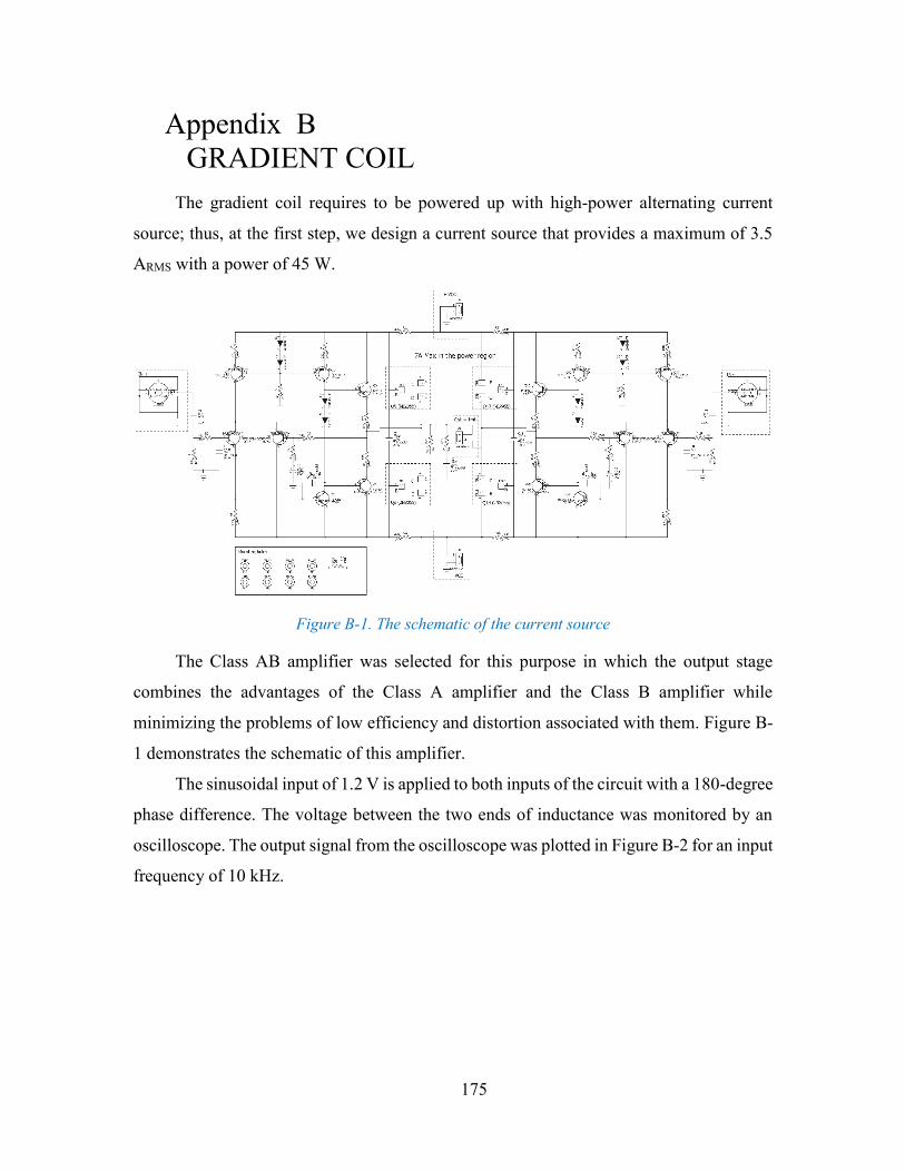
175
Appendix B
GRADIENT COIL
The gradient coil requires to be powered up with high-power alternating current
source; thus, at the first step, we design a current source that provides a maximum of 3.5
ARMS with a power of 45 W.
Figure B-1. The schematic of the current source
The Class AB amplifier was selected for this purpose in which the output stage
combines the advantages of the Class A amplifier and the Class B amplifier while
minimizing the problems of low efficiency and distortion associated with them. Figure B-
1 demonstrates the schematic of this amplifier.
The sinusoidal input of 1.2 V is applied to both inputs of the circuit with a 180-degree
phase difference. The voltage between the two ends of inductance was monitored by an
oscilloscope. The output signal from the oscilloscope was plotted in Figure B-2 for an input
frequency of 10 kHz.
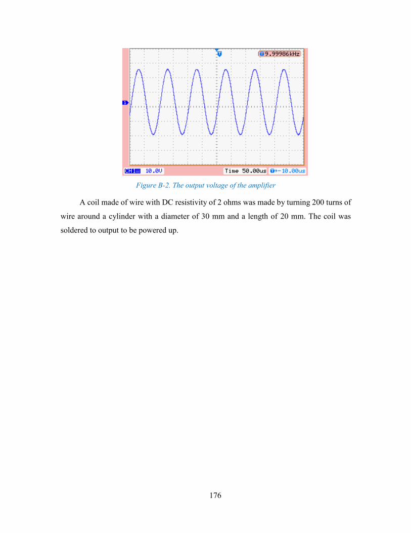
176
Figure B-2. The output voltage of the amplifier
A coil made of wire with DC resistivity of 2 ohms was made by turning 200 turns of
wire around a cylinder with a diameter of 30 mm and a length of 20 mm. The coil was
soldered to output to be powered up.
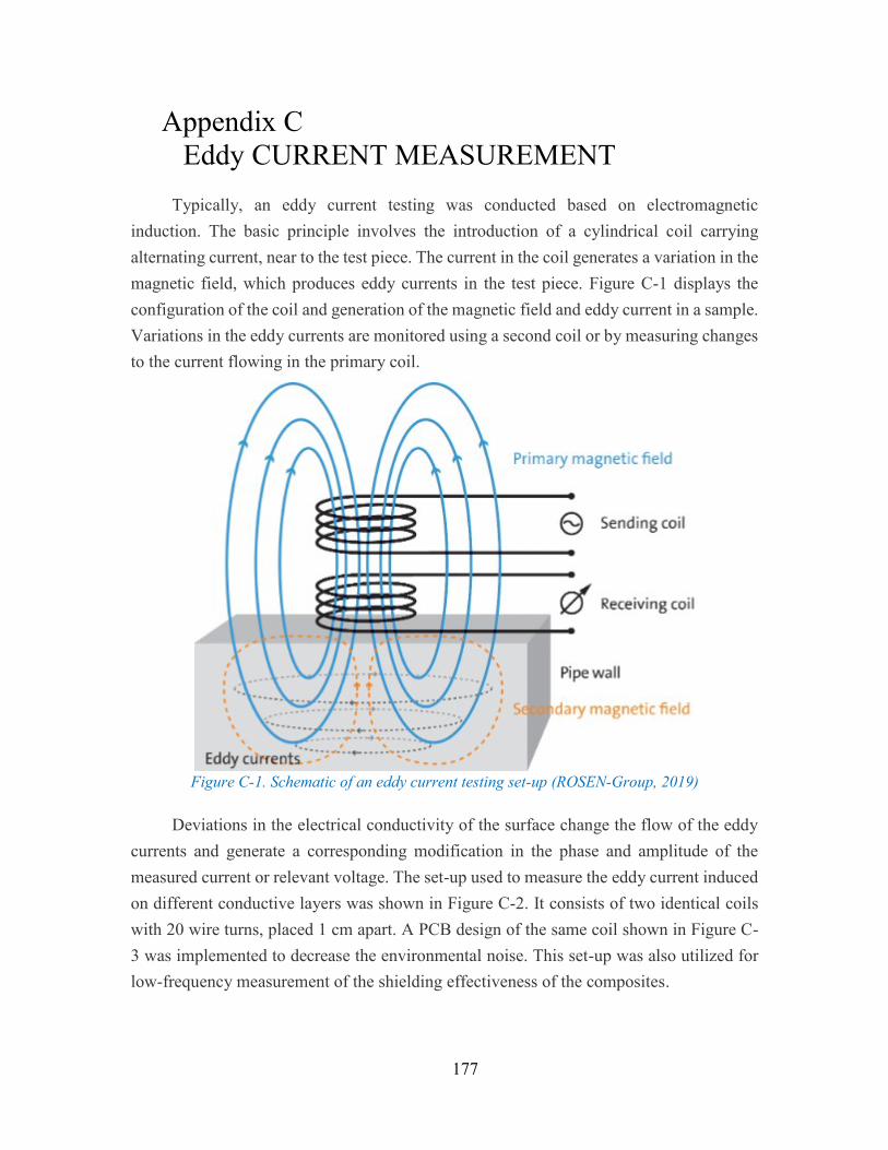
177
Appendix C
Eddy CURRENT MEASUREMENT
Typically, an eddy current testing was conducted based on electromagnetic
induction. The basic principle involves the introduction of a cylindrical coil carrying
alternating current, near to the test piece. The current in the coil generates a variation in the
magnetic field, which produces eddy currents in the test piece. Figure C-1 displays the
configuration of the coil and generation of the magnetic field and eddy current in a sample.
Variations in the eddy currents are monitored using a second coil or by measuring changes
to the current flowing in the primary coil.
Figure C-1. Schematic of an eddy current testing set-up (ROSEN-Group, 2019)
Deviations in the electrical conductivity of the surface change the flow of the eddy
currents and generate a corresponding modification in the phase and amplitude of the
measured current or relevant voltage. The set-up used to measure the eddy current induced
on different conductive layers was shown in Figure C-2. It consists of two identical coils
with 20 wire turns, placed 1 cm apart. A PCB design of the same coil shown in Figure C-
3 was implemented to decrease the environmental noise. This set-up was also utilized for
low-frequency measurement of the shielding effectiveness of the composites.
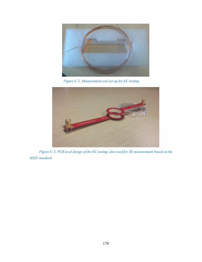
178
Figure C-2. Measurement coil set-up for EC testing
Figure C-3. PCB level design of the EC testing, also used for SE measurement based on the
IEEE standard.
179
REFERENCES
AKESSON, T., ARIK, E., ASSAMAGAN, K., et al. 2001. Particle identification using the
time-over-threshold method in the ATLAS Transition Radiation Tracker. Nuclear
Instruments and Methods in Physics Research Section A: Accelerators,
Spectrometers, Detectors and Associated Equipment, 474, 172-187.
AL-SALEH, M. H., AL-ANID, H. K. & HUSSAIN, Y. A. 2013. CNT/ABS
nanocomposites by solution processing: Proper dispersion and selective
localization for low percolation threshold. Composites Part A: Applied Science and
Manufacturing, 46, 53-59.
ALANEN, A., BONDESTAM, S. & KOMU, M. 1995. Artifacts in MR Imaging Caused
by Small Quantities of Powdered Iron. Acta Radiologica, 36, 92-95.
ANDREWS, R., JACQUES, D., MINOT, M. & RANTELL, T. 2002. Fabrication of
Carbon Multiwall Nanotube/Polymer Composites by Shear Mixing.
Macromolecular Materials and Engineering, 287, 395-403.
ARPIN, L., KOUA, K., PANIER, S., et al. Embedded real time digital signal processing
unit for a 64-channel PET detector module. 2011 IEEE Nuclear Science
Symposium Conference Record, 23-29 Oct. 2011 2011 Valencia, Spain. 1545-
1550.
ASTM 1999. ASTM D4935-99, Standard Test Method for Measuring the Electromagnetic
Shielding Effectiveness of Planar Materials (Withdrawn 2005), ASTM
International, West Conshohocken, PA, www.astm.org.
AVOURIS, P., APPENZELLER, J., MARTEL, R. & WIND, S. J. 2003. Carbon nanotube
electronics. Proceedings of the IEEE, 91, 1772-1784.
AZIZIYAN, M. R., AHMADI, V. & MOGHADAM, N. 2012a. A quantum model for light
emission performance of carbon nanotube field effect transistor. Applied Physics
letter, 100.
AZIZIYAN, M. R., MOGHADAM, N., FATHI, D. & AHMADI, V. 2012b. Analysis of
strained double-lightly doped MOSCNT using NEGF. Applied Physics A, 109, 481-
488.
BENNETT, L., WANG, P. & DONAHUE, M. 1996. Artifacts in magnetic resonance
imaging from metals. Journal of Applied Physics, 79.
BÉRARD, P., BERGERON, M., PEPIN, C. M., et al. 2009. Development of a 64-channel
APD detector module with individual pixel readout for submillimetre spatial
resolution in PET. Nuclear Instruments and Methods in Physics Research Section
A: Accelerators, Spectrometers, Detectors and Associated Equipment, 610, 20-23.
BERARD, P., BERGERON, M., PEPIN, C. M., et al. LabPET II, a novel 64-channel APD-
based PET detector module with individual pixel readout achieving submillimetric
spatial resolution. 2008 IEEE Nuclear Science Symposium Conference Record,
19-25 Oct. 2008 2008 Dresden, Germany. 5457-5462.
BERGERON, M., THIBAUDEAU, C., CADORETTE, J., et al. 2015. LabPET II, an APD-
based Detector Module with PET and Counting CT Imaging Capabilities. IEEE
Transactions on Nuclear Science, 62, 756-765.
180
BERNEKING, A., TRINCHERO, R., HA, Y., et al. 2017. Design and Characterization of
a Gradient-Transparent RF Copper Shield for PET Detector Modules in Hybrid
MR-PET Imaging. IEEE Transactions on Nuclear Science, 64, 1118-1127.
BERNI, A., MENNIG, M. & SCHMIDT, H. 2004. Doctor Blade. In: AEGERTER, M. A.
& MENNIG, M. (eds.) Sol-Gel Technologies for Glass Producers and Users.
Boston, MA: Springer US.
BEYER, T., TOWNSEND, D. W., BRUN, T., et al. 2000. A Combined PET/CT Scanner
for Clinical Oncology. Journal of Nuclear Medicine, 41, 1369-1379.
BOUCHARD, J., ESPAGNET, R., ARPIN, L., et al. 2019. A Low-Profile Positron
Emission Tomography Front End for Submillimetric MRI Insert. 2019 IEEE
Nuclear Science Symposium (NSS) and Medical Imaging Conference (MIC).
Manchester, UK.
BRUNNER, S. E., GRUBER, L., HIRTL, A., et al. 2016. A comprehensive
characterization of the time resolution of the Philips Digital Photon Counter.
Journal of Instrumentation, 11, P11004-P11004.
CALDEIRA, L., ROTA KOPS, E., YUN, S. D., et al. 2018. The Jülich Experience with
Simultaneous 3T MR-BrainPET: Methods and Technology.
CAMACHO, C., PLEWES, D. & HENKELMAN, R. 1995. Nonsusceptibility artifacts due
to metallic objects in MR imaging. Journal of Magnetic Resonance Imaging, 5, 75-
88.
CATANA, C., WU, Y., JUDENHOFER, M. S., et al. 2006. Simultaneous Acquisition of
Multislice PET and MR Images: Initial Results with a MR-Compatible PET
Scanner. Journal of Nuclear Medicine, 47, 1968-1976.
CHANG, C.-M., CATES, J. W. & LEVIN, C. S. 2017. Time-over-threshold for pulse shape
discrimination in a time-of-flight phoswich PET detector. Physics in medicine and
biology, 62, 258-271.
CHAUBEY, M. K., GUPTA, M., HARSH, R. & BHUIYA, T. Multi-channel hexagonal
surface coils for 1.5T MRI scanner. 2016 International Conference on
Communication Systems and Networks (ComNet), 21-23 July 2016 2016. 236-240.
CHEN, C.-C. & TING, C.-C. 2013. Photoelectrode Fabrication of Dye-Sensitized
Nanosolar Cells Using Multiple Spray Coating Technique.
CHEN, G.-X., LI, Y. & SHIMIZU, H. 2007. Ultrahigh-shear processing for the preparation
of polymer/carbon nanotube composites. Carbon, 45, 2334-2340.
CHEN, X. & STECKNER, M. 2017. Electromagnetic computation and modeling in MRI.
Medical Physics, 44, 1186-1203.
CHENG, Q., WANG, B., ZHANG, C. & LIANG, Z. 2010. Functionalized Carbon-
Nanotube Sheet/Bismaleimide Nanocomposites: Mechanical and Electrical
Performance Beyond Carbon-Fiber Composites. Small, 6, 763-767.
CHERRY, S., SORENSON, J. A. & PHELPS, M. E. 2010. Physics in Nuclear Medicine,
ElSEVIER.
CHERRY, S. R., JONES, T., KARP, J. S., et al. 2018. Total-Body PET: Maximizing
Sensitivity to Create New Opportunities for Clinical Research and Patient Care.
Journal of Nuclear Medicine, 59, 3-12.
CHO, Z., KIM, D. & KIM, Y. 1988. Total inhomogeneity correction including chemical
shifts and susceptibility by view angle tilting. Medical Physics, 15, 7-11.
181
CHUNG, D. D. L. 2001. Electromagnetic interference shielding effectiveness of carbon
materials. Carbon, 39, 279-285.
COMSOL, R. 2015. AC/DC Module User’s Guide. COMSOL Multiphysics(R) v.5.2.
COMSOL AB, Stockholm, Sweden, 171-259.
CONECICI, L. M., MUNTEANU, C. & PURCAR, I. M. 2017. Study of the shielding
performances of different materials regarding Electromagnetic Field Interference.
IOP Conference Series: Materials Science and Engineering, 200, 012045.
COSTA, A., APPENZELLER, S., YASUDA, C., et al. 2009. Artifacts in brain magnetic
resonance imaging due to metallic dental objects. Med Oral Patol Oral Cir Buca,
14, 278-82.
COVA, S., GHIONI, M., LACAITA, A., et al. 1996. Avalanche photodiodes and
quenching circuits for single-photon detection. Applied Optics, 35, 1956-1976.
DAMADIAN, R. 1974. Apparatus and method for detection cancer in tissue. USA patent
application.
DELSO, G. & ZIEGLER, S. 2014. PET/MRI: Methodology and Clinical Applications. In:
CARRIO, L. & ROS, P. (eds.) Springer.
DISSELHORST, J. A., BEZRUKOV, I., KOLB, A., et al. 2014. Principles of PET/MR
Imaging. Journal of Nuclear Medicine, 55, 2S-10S.
DOLGOSHEIN, B., BALAGURA, V., BUZHAN, P., et al. 2006. Status report on silicon
photomultiplier development and its applications. Nuclear Instruments and
Methods in Physics Research Section A: Accelerators, Spectrometers, Detectors
and Associated Equipment, 563, 368-376.
DÜPPENBECKER, P. M., WEHNER, J., RENZ, W., et al. Gradient transparent RF
housing for simultaneous PET/MRI using carbon fiber composites. 2012 IEEE
Nuclear Science Symposium and Medical Imaging Conference Record
(NSS/MIC), Oct. 27 2012-Nov. 3 2012 2012 Anaheim, CA, USA. 3478-3480.
DÜPPENBECKER, P. M., WEISSLER, B., GEBHARDT, P., et al. 2016. Development of
an MRI-compatible digital SiPM detector stack for simultaneous PET/MRI.
Biomedical Physics & Engineering Express, 2, 015010.
ESPAGNET, R., BOUCHARD, J., LAKHSSASSI, A., et al. 2019a. Thermal Simulation
of 2.5D Stack-Up with Organic Interposer and Flip Chip for a Preliminary LabPET
II Insert Design. IEEE NSSMIC. Manchester, UK.
ESPAGNET, R., LAKHSSASSI, A., LECOMTE, R. & FONTAINE, R. 2019b. A Thermal
Model of the LabPET II ASIC. IEEE NSSMIC, 2019. Manchester, UK.
FERRARI, A. C., ROBERTSON, J., ZHAO, Q. & WAGNER, H. D. 2004. Raman
spectroscopy of carbon–nanotube–based composites. Philosophical Transactions
of the Royal Society of London. Series A: Mathematical, Physical and Engineering
Sciences, 362, 2407-2424.
FONTAINE, R., ARPIN, L., PAULIN, C., et al. The hardware architecture of the LabPET
II-mouse, a highly integrated APD-based PET scanner. IEEE Nuclear Science
Symposium Medical Imaging Conference, 2016 Strasbourge, French.
FOX, R. T., WANI, V., HOWARD, K. E., et al. 2008. Conductive polymer composite
materials and their utility in electromagnetic shielding applications. Journal of
Applied Polymer Science, 107, 2558-2566.
182
GAUDIN, E., THIBAUDEAU, C., ARPIN, L., et al. 2017. Initial results of a truly
pixelated APD-based PET scanner for high-resolution preclinical imaging. Journal
of Nuclear Medicine, 58, 91.
GAUDIN, E., TOUSSAINT, M., THIBAUDEAU, C., et al. 2019. Performance Simulation
of an Ultrahigh Resolution Brain PET Scanner Using 1.2-mm Pixel Detectors.
IEEE Transactions on Radiation and Plasma Medical Sciences, 3, 334-342.
GEBHARDT, P., WEISSLER, B. & WEHNER, J. 2014. RESCUE - reduction of MR-
SNR-degradation by using an MR-synchronous lowinterfering PET acquisition
technique. EJNMMI Physics 1, Suppl 1:A87.
GILBERT, K. M., SCHOLL, T. J., HANDLER, W. B., et al. 2009. Evaluation of a positron
emission tomography (PET)-compatible field-cycled MRI (FCMRI) scanner.
Magnetic Resonance in Medicine, 62, 1017-1025.
GOERTZEN, A. L. & VAN ELBURG, D. 2019. Performance Characterization of MPPC
Modules for TOF-PET Applications. IEEE Transactions on Radiation and Plasma
Medical Sciences, 3, 475-482.
GONZÁLEZ, M., MOKRY, G., NICOLÁS, M. D., et al. 2016. Carbon Nanotube
Composites as Electromagnetic Shielding Materials in GHz Range. Intechopen.
GOYAT, M. S., RAY, S. & GHOSH, P. K. 2011. Innovative application of ultrasonic
mixing to produce homogeneously mixed nanoparticulate-epoxy composite of
improved physical properties. Composites Part A: Applied Science and
Manufacturing, 42, 1421-1431.
GRAF, H., STEIDLE, G., MARTIROSIAN, P., et al. 2005. Metal artifacts caused by
gradient switching. Magnetic Resonance in Medicine, 54, 231-234.
GRAZIOSO, R., ZHANG, N., CORBEIL, J., et al. 2006. APD-based PET detector for
simultaneous PET/MR imaging. Nuclear Instruments and Methods in Physics
Research Section A: Accelerators, Spectrometers, Detectors and Associated
Equipment, 569, 301-305.
GRECO, S., TAMBURRANO, A., D' ALOIA, A., et al. Shielding effectiveness properties
of carbon-fiber reinforced composite for HIRF applications. International
Symposium on Electromagnetic Compatibility - EMC EUROPE, 17-21 Sept. 2012
2012. 1-6.
HAMMER, B. E., CHRISTENSEN, N. L. & HEIL, B. G. 1994. Use of a magnetic field to
increase the spatial resolution of positron emission tomography. Medical Physics,
21, 1917-1920.
HARGREAVES, B. A., WORTERS, P., PAULY, K., et al. 2011. Metal Induced Artifacts
in MRI. AJR. American journal of roentgenology, 197, 547-555.
HASEGAWA, B. H., GINGOLD, E. L., REILLY, S. M., et al. Description of a
simultaneous emission-transmission CT system. Medical Imaging '90, 1990. SPIE,
11.
HERZOG, H. & VAN DEN HOLF , J. 2012. Combined PET/MR systems: an overview
and comparison of currently available options. J Nucl Med Mol Imaging, 56, 247-
267.
HONG, K., CHOI, Y., JUNG, J., et al. 2013. A prototype MR insertable brain PET using
tileable GAPD arrays. Medical Physics, 40, 042503.
183
HONG, Y. K., LEE, C. Y., JEONG, C. K., et al. 2003. Method and apparatus to measure
electromagnetic interference shielding efficiency and its shielding characteristics
in broadband frequency ranges. Review of Scientific Instruments, 74, 1098-1102.
HU, Z., YANG, W., LIU, H., et al. 2014. From PET/CT to PET/MRI: Advances in
Instrumentation and Clinical Applications. Molecular Pharmaceutics, 11, 3798-
3809.
HUANG, Y. Y., AHIR, S. V. & TERENTJEV, E. M. 2006. Dispersion rheology of carbon
nanotubes in a polymer matrix. Physical Review B, 73, 125422.
HUANG, Y. Y., KNOWLES, T. P. J. & TERENTJEV, E. M. 2009. Strength of Nanotubes,
Filaments, and Nanowires From Sonication-Induced Scission. Advanced Materials,
21, 3945-3948.
HUANG, Y. Y. & TERENTJEV, E. M. 2012. Dispersion of Carbon Nanotubes: Mixing,
Sonication, Stabilization, and Composite Properties. Polymers, 4.
HUANG, Z., PAN, T., GAO, M. & LIN, Y. Chip cooling with carbon nanotube heat sink.
2014 15th International Conference on Electronic Packaging Technology, 12-15
Aug. 2014 2014. 183-185.
IIDA, H., KANNO, I., MIURA, S., et al. 1986. A Simulation Study of a Method to Reduce
Positron Annihilation Spread Distributions Using a Strong Magnetic Field in
Positron Emission Tomography. IEEE Transactions on Nuclear Science, 33, 597-
600.
IPC, O. 2005. IPC-7351: Generic Requirements for Surface Mount Design and Land
Pattern Standard. White paper, IPC Solder Products Value Council.
ISHII, M. & YAMAZAKI, Y. A study on measurement method of shielding effectiveness
using loop antenna in low-frequency. 2014 International Symposium on
Electromagnetic Compatibility, Tokyo, 12-16 May 2014 2014. 749-752.
ISHII, S. High-conductivity boron-doped carbon nanotubes. SPIE, 2007.
JAGATHEESAN, K., RAMASAMY, A., DAS, A. & BASU, A. 2014. Electromagnetic
shielding behaviour of conductive filler composites and conductive fabrics – A
review. Indian Journal of Fibre & Textile Research 39, 329-342.
JUDENHOFER, M. S., WEHRL, H. F., NEWPORT, D. F., et al. 2008. Simultaneous PET-
MRI: a new approach for functional and morphological imaging. Nature Medicine,
14, 459.
KANG, H. G., HONG, S. J., KO, G. B., et al. 2015. Assessment of MR-compatibility of
SiPM PET insert using short optical fiber bundles for small animal research.
Journal of Instrumentation, 10, P12008-P12008.
KANG, J., CHOI, Y., HONG, K. J., et al. Characterization of cross-compatibility of small
animal insertable PET and MRI. 2009 IEEE Nuclear Science Symposium
Conference Record (NSS/MIC), 24 Oct.-1 Nov. 2009 2009 Orlando, FL, USA.
3816-3821.
KE, S., HUANG, H., YU, S. & ZHOU, L. 2010. Crossover from a nearly constant loss to
a superlinear power-law behavior in Mn-doped Bi(Mg1/2Ti1/2)O3–PbTiO3
ferroelectrics. Journal of Applied Physics, 107, 084112.
KIM, H. M., KIM, K., LEE, C. Y., et al. 2004. Electrical conductivity and electromagnetic
interference shielding of multiwalled carbon nanotube composites containing Fe
catalyst. Applied Physics Letters, 84, 589-591.
184
KIM, J. H., HWANG, J. Y., HWANG, H., et al. 2018. Simple and cost-effective method
of highly conductive and elastic carbon nanotube/polydimethylsiloxane composite
for wearable electronics. Scientific Reports, 8, 1375.
KIM, M. S., YAN, J., JOO, K. H., et al. 2013. Synergistic effects of carbon nanotubes and
exfoliated graphite nanoplatelets for electromagnetic interference shielding and
soundproofing. Journal of Applied Polymer Science, 130, 3947-3951.
KINAHAN, P. E., TOWNSEND, D. W., BEYER, T. & SASHIN, D. 1998. Attenuation
correction for a combined 3D PET/CT scanner. Medical Physics, 25, 2046-2053.
KIPNIS, I., COLLINS, T., DEWITT, J., et al. 1997. A time-over-threshold machine: the
readout integrated circuit for the BABAR Silicon Vertex Tracker. IEEE
Transactions on Nuclear Science, 44, 289-297.
KO, G. B., YOON, H. S., KIM, K. Y., et al. 2016. Simultaneous Multiparametric PET/MRI
with Silicon Photomultiplier PET and Ultra-High-Field MRI for Small-Animal
Imaging. Journal of Nuclear Medicine, 57, 1309-1315.
KOCH, K. M., HARGREAVES, B. A., PAULY, K. B., et al. 2010. Magnetic resonance
imaging near metal implants. J Magn Reson Imaging, 32, 773-87.
LAI, R., SABATE, J., CHI, S. & SKEFFINGTON, W. High performance gradient driver
for magnetic resonance imaging system. 2011 IEEE Energy Conversion Congress
and Exposition, 17-22 Sept. 2011 2011. 3511-3515.
LAMEY, M., BURKE, B., BLOSSER, E., et al. 2010. Radio frequency shielding for a
linac-MRI system. Physics in Medicine & Biology, 55, 995.
LAUTERBUR, P. C. 1973. Image Formation by Induced Local Interactions: Examples
Employing Nuclear Magnetic Resonance. Nature, 242, 190.
LECOMTE, R., CADORETTE, J., RODRIGUE, S., et al. 1993. A PET camera simulator
with multispectral data acquisition capabilities. IEEE Transactions on Nuclear
Science, 40, 1067-1074.
LECOMTE, R., DEKEMP, R., KLEIN, R., et al. 2006. LabPET™: A high-performance
APD-based digital PET scanner for small animal imaging. Journal of Nuclear
Medicine, 47, 194P.
LEVIN, D. N., PELIZZARI, C. A., CHEN, G. T., et al. 1988. Retrospective geometric
correlation of MR, CT, and PET images. Radiology, 169, 817-823.
LI, M.-Y., YANG, M., VARGAS, E., et al. 2016. Analysis of variance on thickness and
electrical conductivity measurements of carbon nanotube thin films. Measurement
Science and Technology, 27, 095004.
LI, N., HUANG, Y., DU, F., et al. 2006. Electromagnetic Interference (EMI) Shielding of
Single-Walled Carbon Nanotube Epoxy Composites. Nano Letters, 6, 1141-1145.
LI, P., SHAN, Y., YIN, X., et al. EMI shielding effectiveness of carbon nanotubes based
composites. 2012 Conference on Precision electromagnetic Measurements, 1-6
July 2012 2012. 642-643.
LIPTON, M. L. 2008. Totally Accessible MRI, Springer.
LIVESEY, K. L., CAMLEY, R. E., CELINSKI, Z. & MAAT, S. 2017. Magnetic shielding
of 3-phase current by a composite material at low frequencies. AIP Advances, 7,
056328-1-5.
LLOSA, G., BATTISTON, R., BELCARI, N., et al. 2008. Novel Silicon Photomultipliers
for PET Applications. IEEE Transactions on Nuclear Science, 55, 877-881.
185
LOGAKIS, E., PANDIS, C., PISSIS, P., et al. 2011. Highly conducting poly(methyl
methacrylate)/carbon nanotubes composites: Investigation on their thermal,
dynamic-mechanical, electrical and dielectric properties. Composites Science and
Technology, 71, 854-862.
LU, W., PAULY, K., GOLD, G. E., et al. 2009. SEMAC: Slice encoding for metal artifact
correction in MRI. Magnetic Resonance in Medicine, 62, 66-76.
LUCAS, A. J., HAWKES, R. C., ANSORGE, R. E., et al. 2006. Development of a
Combined microPET®-MR System. Technology in Cancer Research & Treatment,
5, 337-341.
MACKIEWICH, B. 1995.
MAMUNYA, Y. 2011. Carbon Nanotubes as Conductive Filler in Segregated Polymer
Composites - Electrical Properties. InTech, Croatia.
MCLACHLAN, D. S., CHITEME, C., PARK, C., et al. 2005. AC and DC percolative
conductivity of single wall carbon nanotube polymer composites. Journal of
Polymer Science Part B: Polymer Physics, 43, 3273-3287.
MOGHADAM, N., ARPIN, L., ESPAGNET, R., et al. 2019a. Initial MR-Compatibility
Investigation of LabPET II Technology for Simultaneous PET/MRI. submitted to
Physics in Medicine & Biology.
MOGHADAM, N., AZIZIYAN, M. R. & FATHI, D. 2012. Design and simulation of
double-lightly doped MOSCNT using non-equilibrium Green’s function. Applied
Physics A, 108, 551-557.
MOGHADAM, N., ESPAGNET, R., BOUCHARD, J., et al. 2019b. Studying the effects
of metallic components of PET-insert on PET and MRI performance due to gradient
switching. Physics in Medicine & Biology, 64, 075003.
MOGHADAM, N., MORAVVEJ-FARSHI, M. K. & AZIZIYAN, M. R. 2013. Design and
simulation of MOSCNT with band engineered source and drain regions.
Microelectronics Reliability, 53, 533-539.
MURATA, M. 2018. Composition sheet(Eu-RoHS Certificate). 1.
MUSAFARGANI, S., GHOSH, K. K., MISHRA, S., et al. 2018. PET/MRI: a frontier in
era of complementary hybrid imaging. European journal of hybrid imaging, 2, 12-
12.
MUZIC, R. & DIFILIPPO, F. 2014. PET/MRI – Technical Review. Seminars in
roentgenology, 49, 242-254.
NISHIMURA, D. G. 2010. Principle of Magnetic Resonance Imaging, Standford
university.
NJEJIMANA, L., TÉTRAULT, M., ARPIN, L., et al. Design of a real-time FPGA-based
DAQ architecture for the LabPET II, an APD-based scanner dedicated to small
animal PET imaging. 2012 18th IEEE-NPSS Real Time Conference, 9-15 June
2012 2012 Berkeley, CA, USA. 1-5.
OLCOTT, P., KIM, E., HONG, K., et al. 2015. Prototype positron emission tomography
insert with electro-optical signal transmission for simultaneous operation with
MRI. Physics in Medicine and Biology, 60, 3459-3478.
OMIDVARI, N., TOPPING, G., CABELLO, J., et al. 2018. MR-compatibility assessment
of MADPET4: a study of interferences between an SiPM-based PET insert and a 7
T MRI system. Physics in Medicine & Biology, 63, 095002.
186
PARK, S., THEILMANN, P. T., ASBECK, P. M. & BANDARU, P. R. 2010. Enhanced
Electromagnetic Interference Shielding Through the Use of Functionalized Carbon-
Nanotube-Reactive Polymer Composites. IEEE Transactions on Nanotechnology,
9, 464-469.
PARKER-CHOMERICS 2011. Silver/Copper-Filled Acrylic Coating for EMI Shielding
CHO-SHIELD® 2056.
PARKER-CHOMERICS. 2019. Technical specification [Online]. Available:
http://ph.parker.com/ca/en/cho-shield-2056-series-corrosion-resistant-conductive-
coatings [Accessed].
PARL, C., KOLB, A., SCHMID, A. M., et al. 2017. A novel optically transparent RF
shielding for fully integrated PET/MRI systems. Physics in Medicine & Biology,
62, 7357-7378.
PENG, B. J., WALTON, J. H., CHERRY, S. R. & WILLIG-ONWUACHI, J. 2010. Studies
of the interactions of an MRI system with the shielding in a combined PET/MRI
scanner. Physics in medicine and biology, 55, 265-280.
PENG, B. J., WU, Y., CHERRY, S. R. & WALTON, J. H. 2014a. New shielding
configurations for a simultaneous PET/MRI scanner at 7T. Journal of magnetic
resonance (San Diego, Calif. : 1997), 239, 50-56.
PENG, B. J., WU, Y., CHERRY, S. R. & WALTON, J. H. 2014b. New shielding
configurations for a simultaneous PET/MRI scanner at 7T. Journal of Magnetic
Resonance, 239, 50-56.
PICHLER, B., KOLB, A., NÄGELE, T. & SCHLEMMER, H. 2010a. PET/MRI: Paving
the Way for the Next Generation of Clinical Multimodality Imaging Applications.
Journal of Nuclear Medicine, 51, 333-336.
PICHLER, B., LORENZ, E., MIRZOYAN, R., et al. Performance test of a LSO-APD PET
module in a 9.4 Tesla magnet. 1997 IEEE Nuclear Science Symposium Conference
Record, 9-15 Nov 1997 1997 Albuquerque, NM, USA. 1237-1239 vol.2.
PICHLER, B. J., JUDENHOFER, M. S., CATANA, C., et al. 2006. Performance Test of
an LSO-APD Detector in a 7-T MRI Scanner for Simultaneous PET/MRI. Journal
of Nuclear Medicine, 47, 639-647.
PICHLER, B. J., JUDENHOFER, M. S. & WEHRL, H. F. 2008a. PET/MRI hybrid
imaging: devices and initial results. European Radiology, 18, 1077-1086.
PICHLER, B. J., KOLB, A., NÄGELE, T. & SCHLEMMER, H. 2010b. PET/MRI: Paving
the Way for the Next Generation of Clinical Multimodality Imaging Applications.
Journal of Nuclear Medicine, 51, 333-336.
PICHLER, B. J., WEHRL, H. F., KOLB, A. & JUDENHOFER, M. S. 2008b. Positron
Emission Tomography/Magnetic Resonance Imaging: The Next Generation of
Multimodality Imaging? Seminars in Nuclear Medicine, 38, 199-208.
PIEMONTE, C. 2006. A new Silicon Photomultiplier structure for blue light detection.
Nuclear Instruments and Methods in Physics Research Section A: Accelerators,
Spectrometers, Detectors and Associated Equipment, 568, 224-232.
POOLE, M., BOWTELL, R., GREEN, D., et al. 2009. Split gradient coils for simultaneous
PET-MRI. Magnetic resonance in medicine, 62, 1106-1111.
POWOLNY, F., AUFFRAY, E., HILLEMANNS, H., et al. 2008. A Novel Time-Based
Readout Scheme for a Combined PET-CT Detector Using APDs. IEEE
Transactions on Nuclear Science, 55, 2465-2474.
187
RAHAMAN, M., CHAKI, T. & KHASTGIR, D. 2012. Shielding with conductive polymer
and carbon fiber composites.
RENKER, D. 2006. Geiger-mode avalanche photodiodes, history, properties and
problems. Nuclear Instruments and Methods in Physics Research Section A:
Accelerators, Spectrometers, Detectors and Associated Equipment, 567, 48-56.
RENKER, D. 2007. New trends on photodetectors. Nuclear Instruments and Methods in
Physics Research Section A: Accelerators, Spectrometers, Detectors and
Associated Equipment, 571, 1-6.
RICHARD, M. A., FOUQUET, J. P., LEBEL, R. & LEPAGE, M. 2016. MRI-Guided
Derivation of the Input Function for PET Kinetic Modeling. PET Clinics, 11, 193-
202.
ROSEN-GROUP. 2019. EDDY CURRENTMEASUREMENT TECHNOLOGY [Online].
Available: https://www.rosen-group.com/global/company/explore/we-
can/technologies/measurement/eddy-current.html [Accessed].
SAMSON, A., THIBAUDEAU, C., BOUCHARD, J., et al. 2018. A fully automated and
scalable timing probe-based method for time alignment of the LabPET II scanners.
Nuclear Instruments and Methods in Physics Research Section A: Accelerators,
Spectrometers, Detectors and Associated Equipment, 889, 1-6.
SAOUDI, A. & LECOMTE, R. 1999. A novel APD-based detector module for multi-
modality PET/SPECT/CT scanners. IEEE Transactions on Nuclear Science, 46,
479-484.
SARTO, M. S. & TAMBURRANO, A. 2006. Innovative test method for the shielding
effectiveness measurement of conductive thin films in a wide frequency range.
IEEE Transactions on Electromagnetic Compatibility, 48, 331-341.
SASAKI, Y., AKUTAGAWA, M., EMOTO, T., et al. Theoretical study of evaluation
method for MRI metal artifact. 2013 35th Annual International Conference of the
IEEE Engineering in Medicine and Biology Society (EMBC), 3-7 July 2013 2013.
1073-1076.
SCHENCK, J. F. 1996. The role of magnetic susceptibility in magnetic resonance imaging:
MRI magnetic compatibility of the first and second kinds. Medical Physics, 23,
815-850.
SCHLEMMER, H.-P. W., PICHLER, B. J., SCHMAND, M., et al. 2008. Simultaneous
MR/PET Imaging of the Human Brain: Feasibility Study. Radiology, 248, 1028-
1035.
SCHLYER, D., VASKA, P., TOMASI, D., et al. A Simultaneous PET/MRI scanner based
on RatCAP in small animals. 2007 IEEE Nuclear Science Symposium Conference
Record, 26 Oct.-3 Nov. 2007 2007. 3256-3259.
SCHUG, D., LERCHE, C., WEISSLER, B., et al. 2016. Initial PET performance
evaluation of a preclinical insert for PET/MRI with digital SiPM technology.
Physics in Medicine and Biology, 61, 2851-2878.
SCHUG, D., NADIG, V., WEISSLER, B., et al. 2019. Initial Measurements with the
PETsys TOFPET2 ASIC Evaluation Kit and a Characterization of the ASIC TDC.
IEEE Transactions on Radiation and Plasma Medical Sciences, 3, 444-453.
SCHULZ, V., SOLF, T., WEISSLER, B., et al. A preclinical PET/MR insert for a human
3T MR scanner. 2009 IEEE Nuclear Science Symposium Conference Record
(NSS/MIC), Oct. 24 2009-Nov. 1 2009 2009 Orlando, FL, USA. 2577-2579.
188
SCHULZ, V., WEISSLER, B., GEBHARDT, P., et al. SiPM based preclinical PET/MR
insert for a human 3T MR: first imaging experiments. 2011 IEEE Nuclear Science
Symposium Conference Record, 23-29 Oct. 2011 2011. 4467-4469.
SEYDOU TRAORE, M., THIBAUDEAU, C., KOUA, K., et al. 2015. System architecture
of a fully combined PET/CT scanner using LabPET™ electronics with an upgraded
analog front-end optimized for PET and CT counting mode operation. 2015 IEEE
Nuclear Science Symposium and Medical Imaging Conference (NSS/MIC). San
Diego, CA, USA.
SHAFIEI, F., HONDA, E., TAKAHASHI, H. & SASAKI, T. 2003. Artifacts from Dental
Casting Alloys in Magnetic Resonance Imaging. Journal of Dental Research, 82,
602-606.
SHAO, L., CHERRY, S. R., FARAHANI, K., et al. 1997. Development of a PET detector
system compatible with MRI/NMR systems. IEEE Transactions on Nuclear
Science, 44, 1167-1171.
SHAW, N., R., A. & CARPENTER, T. Commissioning and testing of split coil MRI
System for Combined PET-MR. in Proc Intl Soc Mag Reson Med, 2005.
SLOMKA, P. J. 2004. Software Approach to Merging Molecular with Anatomic
Information. Journal of Nuclear Medicine, 45, 36S-45S.
SORET, M., BACHARACH, S. L. & BUVAT, I. 2007. Partial-Volume Effect in PET
Tumor Imaging. Journal of Nuclear Medicine, 48, 932-945.
SPANOUDAKI, V. C., MANN, A. B., OTTE, A. N., et al. 2007. Use of single photon
counting detector arrays in combined PET/MR: Characterization of LYSO-SiPM
detector modules and comparison with a LSO-APD detector. Journal of
Instrumentation, 2, P12002.
SPANOUDAKI, V. C., MCELROY, D. P., TORRES-ESPALLARDO, I. & ZIEGLER, S.
I. 2008. Effect of Temperature on the Performance of Proportional APD-Based
Modules for Gamma Ray Detection in Positron Emission Tomography. IEEE
Transactions on Nuclear Science, 55, 469-480.
STARCUKOVA, J., STARCUK, Z., JR., HUBALKOVA, H. & LINETSKIY, I. 2008.
Magnetic susceptibility and electrical conductivity of metallic dental materials and
their impact on MR imaging artifacts. Dent Mater, 24, 715-23.
STRUL, D., CASH, D., KEEVIL, S. F., et al. 2003. Gamma shielding materials for MR-
compatible PET. IEEE Transactions on Nuclear Science, 50, 60-69.
SUN, K. J., WINCHESKI, R. A. & PARK, C. 2008. Magnetic property measurements on
single wall carbon nanotube polyimide composites. Journal of Applied Physics,
103, 023908.
SUN, X., LIU, X., SHEN, X., et al. 2016. Graphene foam/carbon nanotube/poly(dimethyl
siloxane) composites for exceptional microwave shielding. Composites Part A:
Applied Science and Manufacturing, 85, 199-206.
TAN, C. M., CHEN, S. J. & KONG, J. 2013. Effects of Carbon Loading on the
Performance of Functionalized Carbon Nanotube Polymer Heat Sink for High
Power Light-Emitting Diode in Switching Applications. IEEE Transactions on
Nanotechnology, 12, 1104-1110.
TATSUHIRO, Y., YUHEI, M., JIN, M., et al. 2008. Improved Bath Sonication Method for
Dispersion of Individual Single-Walled Carbon Nanotubes Using New
Triphenylene-Based Surfactant. Japanese Journal of Applied Physics, 47, 2000.
189
TOWNSEND, D. W. 2008. Multimodality imaging of structure and function. Physics in
Medicine & Biology, 53, R1-39.
TRUHN, D., KIESSLING, F. & SCHULZ, V. 2011. Optimized RF shielding techniques
for simultaneous PET/MR. Medical Physics, 38, 3995-4000.
VANDENBERGHE, S. & MARSDEN, P. 2015. PET-MRI: a review of challenges and
solutions in the development of integrated multimodality imaging. Phys Med Biol,
60, R115-54.
VASKA, P. & CAO, T. 2013. The State of Instrumentation for Combined Positron
Emission Tomography and Magnetic Resonance Imaging. Seminars in Nuclear
Medicine, 43, 11-18.
VASQUEZ, H., ESPINOZA, L., LOZANO, K., et al. 2009. Simple device for
electromagnetic interference shielding effectiveness measurement. IEEE EMC
Society Newsletter, 220, 62-68.
VEIT-HAIBACH, P., KUHN, F. P., WIESINGER, F., et al. 2013. PET–MR imaging using
a tri-modality PET/CT–MR system with a dedicated shuttle in clinical routine.
Magnetic Resonance Materials in Physics, Biology and Medicine, 26, 25-35.
WANG, X., YONG, Z. Z., LI, Q. W., et al. 2013. Ultrastrong, Stiff and Multifunctional
Carbon Nanotube Composites. Materials Research Letters, 1, 19-25.
WEHRL, H., JUDENHOFER, M., THIELSCHER, A., et al. 2011. Assessment of MR
compatibility of a PET insert developed for simultaneous multiparametric PET/MR
imaging on an animal system operating at 7 T. Magnetic Resonance in Medicine,
65, 269-279.
WEIRICH, C., BRENNER, D., SCHEINS, J., et al. 2012. Analysis and Correction of
Count Rate Reduction During Simultaneous MR-PET Measurements With the
BrainPET Scanner. IEEE Transactions on Medical Imaging, 31, 1372-1380.
WEISSLER, B., GEBHARDT, P., DÜPPENBECKER, P., et al. Design concept of world's
first preclinical PET/MR insert with fully digital silicon photomultiplier
technology. 2012 IEEE Nuclear Science Symposium and Medical Imaging
Conference Record (NSS/MIC), 27 Oct.-3 Nov. 2012 2012. 2113-2116.
YAMAMOTO, S., KURODA, K. & SENDA, M. Scintillator selection for MR compatible
gamma detectors. 2002 IEEE Nuclear Science Symposium Conference Record,
10-16 Nov. 2002 2002. 1632-1635 vol.3.
YAMAMOTO, S., KURODA, K. & SENDA, M. 2003. Scintillator selection for MR-
compatible gamma detectors. IEEE Transactions on Nuclear Science, 50, 1683-
1685.
YAMAMOTO, S., WATABE, H., KANAI, Y., et al. 2011. Interference between PET and
MRI sub-systems in a silicon-photomultiplier-based PET/MRI system. Physics in
Medicine & Biology, 56, 4147.
YANG, C. Q., WU, Z. S. & HUANG, H. 2007. Electrical properties of different types of
carbon fiber reinforced plastics (CFRPs) and hybrid CFRPs. Carbon, 45, 3027-
3035.
YANG, Y., GUPTA, M. C., DUDLEY, K. L. & LAWRENCE, R. W. 2005. A Comparative
Study of EMI Shielding Properties of Carbon Nanofiber and Multi-Walled Carbon
Nanotube Filled Polymer Composites. Journal of Nanoscience and
Nanotechnology, 5, 927-931.
190
YIPING, S., SIMON, R. C., KEYVAN, F., et al. 1997. Simultaneous PET and MR
imaging. Physics in Medicine & Biology, 42, 1965.
YOUM, K. H. & LEE, S.-I. 1991. A.C. conductivity and dielectric constant in a two-
dimensional Swiss cheese percolation system. Solid State Communications, 79,
1069-1072.
ZAIDI, H. & DEL GUERRA, A. 2011. An outlook on future design of hybrid PET/MRI
systems. Medical Physics, 38, 5667-5689.
ZAIDI, H., OJHA, N., MORICH, M., et al. 2011. Design and performance evaluation of a
whole-body Ingenuity TF PET–MRI system. Physics in Medicine & Biology, 56,
3091.
ZHOU, Y. X., WU, P. X., CHENG, Z.-Y., et al. 2008. Improvement in electrical, thermal
and mechanical properties of epoxy by filling carbon nanotube. eXPRESS Polymer
Letters, 2, 40-48.