Embed Size (px)
Citation preview

VTM48Ex120y025A0RVTM™ Current Multiplier
High-Efficiency, Bidirectional Sine Amplitude Converter
VTM™ Current Multiplier Rev 1.3Page 1 of 20 06/2018
S
NRTLC USC US®
Features & Benefits
• 48VDC to 12VDC 25A bidirectional current multiplier
• Can power a load connected to either the primary or secondary side
• High efficiency (>96%) reduces system power consumption
• High density (85A/in3)
• “Full Chip” VI Chip® package enables surface mount, low-impedance interconnect to system board
• Contains built-in protection features against:
�� Overvoltage Lockout�� Overcurrent�� Short Circuit�� Overtemperature
• Provides enable / disable control, internal temperature monitoring
• ZVS / ZCS resonant Sine Amplitude Converter topology
• Less than 50ºC temperature rise at full load in typical applications
Typical Applications
• High-End Computing Systems
• Automated Test Equipment
• High-Density Power Supplies
• Communications Systems
Product Description
The VI Chip® bidirectional current multiplier is a Sine Amplitude Converter (SAC™) operating from a 26 to 55VDC primary source or a 6.5 to 13.8VDC secondary source to power a load. The bidirectional Sine Amplitude Converter isolates and transforms voltage at a secondary:primary ratio of 1/4. The SAC offers a low AC impedance beyond the bandwidth of most downstream regulators; therefore for a step-down conversion; capacitance normally at the load can be located at the source to the Sine Amplitude Converter to enable a reduction in size of capacitors. Since the K factor of the VTM48EF120T025A0R is 1/4, the capacitance value on the primary side can be reduced by a factor of 16 in an application where the source is located on the primary side, resulting in savings of board area, materials and total system cost.
The VTM48EF120T025A0R is provided in a VI Chip package compatible with standard pick-and-place and surface mount assembly processes. The co-molded VI Chip package provides enhanced thermal management due to a large thermal interface area and superior thermal conductivity. The high conversion efficiency of the VTM48EF120T025A0R increases overall system efficiency and lowers operating costs compared to conventional approaches.
The VTM48EF120T025A0R enables the utilization of Factorized Power Architecture™ which provides efficiency and size benefits by lowering conversion and distribution losses and promoting high-density point-of-load conversion.
+INEnable
–IN
+OUT
–OUT
+INEnable
–IN
+OUT
–OUT
+PRI
–PRI
+SEC
–SEC
VTM
PRM A
PRM B
BatteryFor Storage and Operating Temperatures see General Characteristics Section
Typical Application
Product Ratings
VPRI = 26 – 55V ISEC = 25A (Nominal)
VSEC = 6.5 – 13.8V (No Load) K = 1/4
Product Number Package Style (x) Product Grade (y)
VTM48Ex120y025A0RF = J-Lead T = –40 to 125°C
T = Through hole M = –55 to 125°C
Part Numbering

VTM™ Current Multiplier Rev 1.3Page 2 of 20 06/2018
VTM48Ex120y025A0R
Absolute Maximum Ratings
The absolute maximum ratings below are stress ratings only. Operation at or beyond these maximum ratings can cause permanent damage to the device.
Parameter Comments MPRI Max Unit
+PRI to –PRI –1.0 60 VDC
PC to –PRI –0.3 20 VDC
TM to –PRI –0.3 7 VDC
VC to –PRI –0.3 20 VDC
+PRI / –PRI to +SEC / –SEC (hipot) 2250 VDC
+SEC to –SEC –1.0 16 VDC
Primary-Source Electrical Specifications
Specifications apply over all line and load conditions unless otherwise noted; boldface specifications apply over the temperature range of –40°C < TJ < 125°C (T-Grade). All other specifications are at TJ = 25ºC unless otherwise noted.
Attribute Symbol Conditions / Notes Min Typ Max Unit
Powertrain
Primary Voltage Range VPRI
No external VC applied 26 55VDC
VC applied 0 55
VPRI Slew Rate dVPRI / dt 1 V / µs
VPRI UV Turn Off VPRI_UVModule latched shutdown, No external VC applied, ISEC = 25A
24 26 V
No Load Power Dissipation PNL
VPRI = 48V 3 15.0
WVPRI = 26 – 55V 17
VPRI = 48V, TC = 25ºC 5.3 6.5
VPRI = 26 – 55V, TC = 25ºC 9
Inrush Current Peak IINRPVC enable, VPRI = 48V, CSEC = 1000µF, RLOAD = 471mΩ
10 20 A
DC Primary Current IPRI_DC 7 A
Transfer Ratio K K = VSEC / VPRI, ISEC = 0A 1/4 V / V
Secondary Voltage VSEC VSEC = VPRI • K – ISEC • RSEC V
Secondary Current (Average) ISEC_AVG 25 A
Secondary Current (Peak) ISEC_PK tPEAK < 10ms, ISEC_AVG ≤ 25A 37.5 A
Secondary Power (Average) PSEC_AVG ISEC_AVG ≤ 25A 300 W
Efficiency (Ambient) ηAMB
VPRI = 48V, ISEC = 25A 95.0 96.0
%VPRI = 26 – 55V, ISEC = 25A 93.0
VPRI = 48V, ISEC = 12.5A 94.5 95.5
Efficiency (Hot) ηHOT VPRI = 48V, TC = 100°C, ISEC = 25A 94.5 95.6 %
Efficiency (Over Load Range) η20% 5A < ISEC < 25A 80.0 %

VTM™ Current Multiplier Rev 1.3Page 3 of 20 06/2018
VTM48Ex120y025A0R
Primary-Source Electrical Specifications (Cont.)
Specifications apply over all line and load conditions unless otherwise noted; boldface specifications apply over the temperature range of –40°C < TJ < 125°C (T-Grade). All other specifications are at TJ = 25ºC unless otherwise noted.
Attribute Symbol Conditions / Notes Min Typ Max Unit
Powertrain (Cont.)
Secondary Resistance (Cold) RSEC_COLD TC = –40°C, ISEC = 25A 4.9 7.5 12.0 mΩ
Secondary Resistance (Ambient) RSEC_AMB TC = 25°C, ISEC = 25A 6.3 9.0 14.0 mΩ
Secondary Resistance (Hot) RSEC_HOT TC = 100°C, ISEC = 25A 8.8 11.5 16.0 mΩ
Switching Frequency FSW 1.85 1.95 2.05 MHz
Secondary Ripple Frequency FSW_RP 3.70 3.90 4.10 MHz
Secondary Voltage Ripple VSEC_PP CSEC = 0F, ISEC = 25A, VPRI = 48V, 20MHz BW 150 285 mV
Secondary Inductance (Parasitic) LSEC_PAR Frequency up to 30MHz, Simulated J-lead model 600 pH
Secondary Capacitance (Internal) CSEC_INT Effective Value at 12VSEC 47 µF
Secondary Capacitance (External) CSEC_EXT VTM Standalone Operation. VPRI pre-applied, VC enable 1000 µF
Protection
Primary Overvoltage Lockout VPRI_OVLO+ Module latched shutdown 55.1 58.5 60.0 V
Primary Overvoltage Lockout Response Time Constant
tOVLO Effective internal RC filter 8 µs
Secondary Overcurrent Trip IOCP_SEC 39 47 A
Secondary Short Circuit Protection Trip Current
ISCP_SEC 39 A
Secondary Overcurrent Response Time Constant
tOCP_SEC Effective internal RC filter (Integrative) 5.3 ms
Secondary Short Circuit Protection Response Time
tSCP_SECFrom detection to cessation of switching (Instantaneous)
1 µs
Thermal Shutdown Set Point TJ_OTP 125 130 135 °C

VTM™ Current Multiplier Rev 1.3Page 4 of 20 06/2018
VTM48Ex120y025A0R
Secondary-Source Electrical Specifications
Specifications apply over all line and load conditions unless otherwise noted; boldface specifications apply over the temperature range of –40°C < TJ < 125°C (T-Grade). All other specifications are at TJ = 25ºC unless otherwise noted.
Attribute Symbol Conditions / Notes Min Typ Max Unit
Powertrain
Secondary Voltage Range VSEC
No external VC applied 6.5 13.75VDC
VC applied 0 13.75
VSEC Slew Rate dVSEC / dt 1 V / µs
VSEC UV Turn Off VSEC_UVModule latched shutdown, No external VC applied, IPRI = 6.3A
6.0 6.5 V
No Load Power Dissipation PNL_SEC
VSEC = 12V 3 15.0
WVSEC = 6.5 – 13.75V 17.0
VSEC = 12V, TC = 25ºC 5.3 6.5
VSEC = 6.5 – 13.75V, TC = 25ºC 9.0
Inrush Current Peak INR_SEC_PVC enable, VSEC = 12V, CPRI = 63µF, RLOAD = 7mΩ
40 80 A
DC Secondary Current ISEC_DC 28.0 A
Primary Voltage VPRI VPRI = VSEC / K – IPRI • RPRI V
Primary Current (Average) IPRI_AVG 6.3 A
Primary Current (Peak) IPRI_PK tPEAK < 10ms, IPRI_AVG ≤ 6.3A 9.4 A
Primary Power (Average) PPRI_AVG IPRI_AVG ≤ 6.3A 300 W
Efficiency (Ambient) ηAMB
VSEC = 12V, IPRI = 6.3A 95 96.0
%VSEC = 6.5 – 13.75V, IPRI = 6.3A 93
VSEC = 12V, IPRI = 3.1A 94.5 95.5
Efficiency (Hot) ηHOT VSEC = 12V, TC = 100°C, IPRI = 6.3A 94.5 95.6 %
Efficiency (Over Load Range) η20% 1.3A < IPRI < 6.3A 80.0 %
Primary Resistance (Cold) RPRI_COLD TC = –40°C, IPRI = 6.3A 145 165 185 mΩ
Primary Resistance (Ambient) RPRI_AMB TC = 25°C, IPRI = 6.3A 165 195 225 mΩ
Primary Resistance (Hot) RPRI_HOT TC = 100°C, IPRI = 6.3A 200 238 275 mΩ
Primary Voltage Ripple VPRI_PP CPRI = 0F, IPRI = 6.3A, VSEC = 12V, 6.5MHz BW 650 mV
Primary Capacitance (External) CPRI_EXTVTM Standalone Operation. VSEC pre-applied, VC enable 63 µF
Protection
Secondary Overvoltage Lockout VSEC_OVLO+ Module latched shutdown 14.5 14.8 15.0 V
Secondary Overvoltage Lockout Response Time Constant
tOVLO_SEC Effective internal RC filter 8 µs
Primary Overcurrent Trip IOCP_PRI 7 9 14 A
Primary Short Circuit Protection Trip Current
ISCP_PRI 7 A
Primary Overcurrent Response Time Constant
tOCP_PRI Effective internal RC filter (Integrative) 5.3 ms
Primary Short Circuit Protection Response Time
tSCP_PRIFrom detection to cessation of switching (Instantaneous)
1 µs

VTM™ Current Multiplier Rev 1.3Page 5 of 20 06/2018
VTM48Ex120y025A0R
Signal Characteristics
Specifications apply over all line and load conditions unless otherwise noted; boldface specifications apply over the temperature range of –40°C ≤ TJ < 125°C (T-Grade). All other specifications are at TJ = 25ºC unless otherwise noted.
VTM Control: VC
• Referenced to –PRI• Used to wake up powertrain circuit.• A minimum of 11.5V must be applied indefinitely for VPRI < 26V to ensure normal operation.• VC slew rate must be within range for a successful start.• PRM™ VC can be used as valid wake-up signal source.• Internal Resistance used in “Adaptive Loop” compensation.• VC voltage may be continuously applied.
Signal Type State Attribute Symbol Conditions / Notes Min Typ Max Unit
ANALOG
INPUT
Steady
External VC Voltage VVC_EXTRequired for start up and operation below 26V.
11.5 16.5 V
VC Current Draw IVC
VC = 11.5V, VPRI = 0V 130 150
mAVC = 11.5V, VPRI > 26V 25
VC = 16.5V, VPRI > 26V 115
Fault mode. VC > 11.5V 60
VC Internal Diode Rating DVC_INT 100 V
VC Internal Resistor RVC-INT 0.511 kΩ
VC Internal ResistorTemperature Coefficient
TVC_COEFF 3900 ppm/°C
Start Up
VC Start-Up Pulse VVC_SP tPEAK < 18ms 20 V
VC Slew Rate dVC/dt Required for proper start up 0.02 0.25 V / µs
VC Inrush Current IINR_VC VC = 16.5V, dVC/dt = 0.25V/μs 1 A
Transitional
VC to VSEC Turn-On Delay tONVPRI pre-applied, PC floating, VC enable, CPC = 0μF
500 µs
VC to PC Delay tVC_PCVC = 11.5V to PC high, VPRI = 0V, dVC/dt = 0.25V/μs
75 125 µs
Internal VC Capacitance CVC_INT VC = 0V 3.2 µF
Primary Control: PC
• Referenced to –PRI• The PC pin enables and disables the VTM. When held below 2V, the VTM will be disabled.• PC pin outputs 5V during normal operation. PC pin is equal to 2.5V during fault mode given VPRI > 26V or VC > 11.5V.• After successful start up and under no-fault condition, PC can be used as a 5V regulated voltage source with a 2mA maximum current.• Module will shutdown when pulled low with an impedance less than 400Ω.• In an array of VTMs, connect PC pin to synchronize start up.• PC pin cannot sink current and will not disable other modules during fault mode.
Signal Type State Attribute Symbol Conditions / Notes Min Typ Max Unit
ANALOG
OUTPUT
Steady
PC Voltage VPC 4.7 5.0 5.3 V
PC Source Current IPC_OP 2 mA
PC Resistance (Internal) RPC_INT Internal pull-down resistor 50 150 400 kΩ
Start Up
PC Source Current IPC_EN 50 100 300 µA
PC Capacitance (Internal) CPC_INT 1000 pF
PC Resistance (External) RPC_S 60 kΩ
DIGITAL
INPUT /
OUTPUT
Enable PC Voltage VPC_EN 2 2.5 3 V
DisablePC Voltage (Disable) VPC_DIS 2 V
PC Pull-Down Current IPC_PD 5.1 mA
TransitionalPC Disable Time tPC_DIS_T 5 µs
PC Fault-Response Time tFR_PC From fault to PC = 2V 100 µs

VTM™ Current Multiplier Rev 1.3Page 6 of 20 06/2018
VTM48Ex120y025A0R
Signal Characteristics (Cont.)
Specifications apply over all line and load conditions unless otherwise noted; boldface specifications apply over the temperature range of –40°C ≤ TJ < 125°C (T-Grade). All other specifications are at TJ = 25ºC unless otherwise noted.
Temperature Monitor: TM
• Referenced to –PRI• The TM pin monitors the internal temperature of the VTM controller IC within an accuracy of ±5°C. • Can be used as a “Power Good” flag to verify that the VTM is operating.• The TM pin has a room-temperature set point of 3V and approximate gain of 10mV/°C.• Output drives Temperature Shutdown comparator.
Signal Type State Attribute Symbol Conditions / Notes Min Typ Max Unit
ANALOG
OUTPUTSteady
TM Voltage VTM_AMB TJ controller = 27°C 2.95 3.00 3.05 V
TM Source Current ITM 100 µA
TM Gain ATM 10 mV/°C
TM Voltage Ripple VTM_PP CTM = 0F, VPRI = 48V, ISEC = 25A 120 200 mV
DIGITAL
OUTPUT
(FAULT FLAG)
Disable TM Voltage VTM_DIS 0 V
Transitional
TM Resistance (Internal) RTM_INT Internal pull-down resistor 25 40 50 kΩ
TM Capacitance (External) CTM_EXT 50 pF
TM Fault-Response Time tFR_TM From fault to TM = 1.5V 10 µs

VTM™ Current Multiplier Rev 1.3Page 7 of 20 06/2018
VTM48Ex120y025A0R
Timing Diagram
Power sourced from the primary side.
1 2
7
VPRI
1. Initiated VC pulse2. Controller start3. VPRI ramp up4. VPRI = VOVLO5. VPRI ramp down no VC pulse6. Overcurrent, Secondary7. Start up on short circuit8. PC driven low
VSEC
PC
3V
VC
NL
5V
VOVLO
TMVTM-AMB
c
Notes: – Timing and voltage is not to scale – Error pulse width is load dependent
a: VC slew rate (dVC/dt) b: Minimum VC pulse ratec: tOVLO_PIN
d: tOCP_SEC
e: Secondary turn on delay (tON)f: PC disable time (tPC_DIS_t)g: VC to PC delay (tVC_PC)
d
ISEC
ISEC
ISEC
VVC-EXT
3 4 5
6
a
b
8
g
e f
≥ 26V

VTM™ Current Multiplier Rev 1.3Page 8 of 20 06/2018
VTM48Ex120y025A0R
Application Characteristics
The following values, typical of an application environment, are collected at TC = 25ºC with power sourced from the primary side unless otherwise noted. See associated figures for general trend data.
Attribute Symbol Conditions / Notes Typ Unit
Powertrain
No-Load Power Dissipation PNL VPRI = 48V, PC enabled 5.1 W
Efficiency (Ambient) ηAMB VPRI = 48V, ISEC = 25A 96.1 %
Efficiency (Hot) ηHOT VPRI = 48V, ISEC = 25A, TC = 100ºC 95.6 %
Secondary Resistance (Cold) RSEC_COLD VPRI = 48V, ISEC = 25A, TC = –40ºC 7.3 mΩ
Secondary Resistance (Ambient) RSEC_AMB VPRI = 48V, ISEC = 25A 9.3 mΩ
Secondary Resistance (Hot) RSEC_HOT VPRI = 48V, ISEC = 25A, TC = 100ºC 11.6 mΩ
Secondary Voltage Ripple VSEC_PP CSEC = 0F, ISEC = 25A, VPRI = 48V, 20MHz BW 198 mV
VSEC Transient (Positive) VSEC_TRAN+ ISEC_STEP = 0 – 25A, VPRI = 48V, ISLEW = 17A/µs 650 mV
VSEC Transient (Negative) VSEC_TRAN– ISEC_STEP = 25 – 0A, VPRI = 48V, ISLEW = 212A/µs 310 mV
Input Voltage (V)
Pow
er D
issi
patio
n (W
)
–40°C 25°C 100°CTCASE:
1
3
9
11
5
7
26 29 32 35 38 41 43 46 49 52 55
Full
Load
Effi
cien
cy (%
)
9293
95
9190
94
96
979899
100
–40 –20 0 20 40 60 80 100Case Temperature (ºC)
26V 48V 55VVPRI:
Secondary Load Current (A)
Effic
ienc
y (%
)
26V 48V 55VVPRI:
606468
7276808488
9296
100
0 2.5 5 7.5 10 12.5 17.5 22.515 20 25Secondary Load Current (A)
Pow
er D
issi
patio
n (W
)
26V 48V 55VVPRI:
05
1015202530354045
50
0 2.5 5 7.5 10 12.5 17.5 22.515 20 25
Figure 1 — No load power dissipation vs. VPRI Figure 2 — Full load efficiency vs. temperature
Figure 3 — Efficiency at –40°C Figure 4 — Power dissipation at –40°C

VTM™ Current Multiplier Rev 1.3Page 9 of 20 06/2018
VTM48Ex120y025A0R
Application Characteristics (Cont.)
The following values, typical of an application environment, are collected at TC = 25ºC with power sourced from the primary side unless otherwise noted. See associated figures for general trend data.
Secondary Load Current (A)
V RIP
PLE (
mV PK
-PK)
26V 48V 55VVPRI:
75
100
50
125
150
175
200
225
250
0 2.5 5 7.5 10 12.5 17.5 22.515 20 25
Figure 10 — Vripple vs. ISEC; No external CSEC. Board mounted module, scope setting: 20MHz analog BW
Secondary Load Current (A)
Effic
ienc
y (%
)
26V 48V 55VVPRI:
68
72
76
80
84
88
92
96
100
0 2.5 5 7.5 10 12.5 17.5 22.515 20 25Secondary Load Current (A)
Pow
er D
issi
patio
n (W
)
26V 48V 55VVPRI:
0
4
8
12
16
20
24
28
32
0 2.5 5 7.5 10 12.5 17.5 22.515 20 25
Case Temperature (ºC)
RSE
C (m
Ω)
12.5A 25AISEC:
4
10
12
6
8
14
–40 –20 0 20 40 8060 100
Figure 7 — Efficiency at 100°C Figure 8 — Power dissipation at 100°C
Figure 9 — RSEC vs. temperature
Secondary Load Current (A)
Effic
ienc
y (%
)
26V 48V 55VVPRI:
68
72
76
80
84
88
92
96
100
0 2.5 5 7.5 10 12.5 17.5 22.515 20 25Secondary Load Current (A)
Pow
er D
issi
patio
n (W
)
26V 48V 55VVPRI:
0
4
8
12
16
20
24
28
32
0 2.5 5 7.5 10 12.5 17.5 22.515 20 25
Figure 5 — Efficiency at 25°C Figure 6 — Power dissipation at 25°C

VTM™ Current Multiplier Rev 1.3Page 10 of 20 06/2018
VTM48Ex120y025A0R
Figure 13 — Start up from application of VPRI; VC pre-applied CSEC = 1000µF
Secondary Voltage (V)
Seco
ndar
y C
urre
nt (A
)
0
10
5
20
15
25
30
35
40
45
0 2 4 6 8 10 12 14 16
Continuous
10ms max
Figure 11 — Safe operating area Figure 12 — Full load ripple, 100µF CPRI; No external CSEC. Board- mounted module, scope setting: 20MHz analog BW
Figure 16 — Full load – 0A transient response: CPRI = 100µF, no external CSEC
Figure 15 — 0A – Full load transient response: CPRI = 100µF, no external CSEC
Figure 14 — Start up from application of VC; VPRI pre-applied CSEC = 1000µF
Application Characteristics (Cont.)
The following values, typical of an application environment, are collected at TC = 25ºC with power sourced from the primary side unless otherwise noted. See associated figures for general trend data.

VTM™ Current Multiplier Rev 1.3Page 11 of 20 06/2018
VTM48Ex120y025A0R
General Characteristics
Specifications apply over all line and load conditions unless otherwise noted; boldface specifications apply over the temperature range of –40ºC < TJ < 125 ºC (T-Grade). All Other specifications are at TJ = 25°C unless otherwise noted.
Attribute Symbol Conditions / Notes Min Typ Max Unit
Mechanical
Length L 32.25 [1.270] 32.5 [1.280] 32.75 [1.289] mm [in]
Width W 21.75 [0.856] 22.0 [0.866] 22.25 [0.876] mm [in]
Height H 6.48 [0.255] 6.73 [0.265] 6.98 [0.275] mm [in]
Volume Vol No heat sink 4.81 [0.294] cm3 [in3]
Weight W 15.0 [0.53] g [oz]
Lead Finish
Nickel 0.51 2.03
µmPalladium 0.02 0.15
Gold 0.003 0.051
Thermal
Operating Temperature TJ
VTM48EF120T025A0R (T-Grade) –40 125
°CVTM48EF120M025A0R (M-Grade) –55 125
VTM48ET120T025A0R (T-Grade) –40 125
VTM48ET120M025A0R (M-Grade) –55 125
Thermal Resistance θJC
Isothermal heat sink and isothermal internal PCB
1 °C / W
Thermal Capacity 5 Ws / °C
Assembly
Peak Compressive Force Applied to Case (Z-Axis)
Supported by J-Lead only6 lbs
5.41 lbs / in2
Storage Temperature TST
VTM48EF120T025A0R (T-Grade) –40 125
°CVTM48EF120M025A0R (M-Grade) –65 125
VTM48ET120T025A0R (T-Grade) –40 125
VTM48ET120M025A0R (M-Grade) –65 125
ESD WithstandESDHBM
Human Body Model,JEDEC JESD 22-A114-F
1000VDC
ESDCDMCharge Device Model,JEDEC JESD 22-C101-D
400
Soldering
Peak Temperature During Reflow MSL 4 (Datecode 1528 and later) 245 °C
Peak Time Above 217°C 60 90 s
Peak Heating Rate During Reflow 1.5 3 °C / s
Peak Cooling Rate Post Reflow 1.5 6 °C / s
Safety
Isolation Voltage (Hipot) VHIPOT 2250 VDC
Isolation Capacitance CPRI_SEC Unpowered unit 2500 3200 3800 pF
Isolation Resistance RPRI_SEC 10 MΩ
MTBF
MIL-HDBK-217 Plus Parts Count;25ºC Ground Benign, Stationary,Indoors / Computer Profile
6.03 MHrs
Telcordia Issue 2 - Method I Case 1;Ground Benign, Controlled
7.94 MHrs
Agency Approvals / Standards
cTÜVus EN 60950-1
cURus UL 60950-1
CE Marked for Low Voltage Directive and RoHS Recast Directive, as applicable

VTM™ Current Multiplier Rev 1.3Page 12 of 20 06/2018
VTM48Ex120y025A0R
Using the Control Signals VC, PC, TM
The VTM Control (VC) pin is a primary-referenced pin which powers the internal VCC circuitry when within the specified voltage range of 11.5 – 16.5V. This voltage is required for VTM current multiplier start up and must be applied as long as the primary is below 26V. In order to ensure a proper start, the slew rate of the applied voltage must be within the specified range.
Some additional notes on the using the VC pin:
�� In most applications, the VTM module primary side will be powered by an upstream PRM™ regulator which provides a 10ms VC pulse during start up. In these applications the VC pins of the PRM regulator and VTM current multiplier should be tied together.
�� In bidirectional applications, the primary of the VTM may also be providing power to a PRM input. In these applications, a proper VC voltage within the specified range must be applied any time the primary voltage of the VTM is below 26V.
�� The VC voltage can be applied indefinitely allowing for continuous operation down to 0VPRI.
�� The fault response of the VTM module is latching. A positive edge on VC is required in order to restart the unit. If VC is continuously applied the PC pin may be toggled to restart the VTM module.
Primary Control (PC) is a primary-referenced pin that can be used to accomplish the following functions:
�� Delayed start: Upon the application of VC, the PC pin will source a constant 100µA current to the internal RC network. Adding an external capacitor will allow further delay in reaching the 2.5V threshold for module start.
�� Auxiliary voltage source: Once enabled in regular operational conditions (no fault), each VTM PC provides a regulated 5V, 2mA voltage source.
�� Disable: PC pin can be actively pulled down in order to disable the module. Pull-down impedance shall be lower than 400Ω.
�� Fault detection flag: The PC 5V voltage source is internally turned off as soon as a fault is detected. It is important to notice that PC doesn’t have current sink capability. Therefore, in an array, PC line will not be capable of disabling neighboring modules if a fault is detected.
�� Fault reset: PC may be toggled to restart the unit if VC is continuously applied.
Temperature Monitor (TM) is a primary-referenced pin that provides a voltage proportional to the absolute temperature of the converter control IC.
It can be used to accomplish the following functions:
�� Monitor the control IC temperature: The temperature in Kelvin is equal to the voltage on the TM pin scaled by 100. (i.e., 3.0V = 300K = 27ºC). If a heat sink is applied, TM can be used to thermally protect the system.
�� Fault detection flag: The TM voltage source is internally turned off as soon as a fault is detected. For system monitoring purposes (microcontroller interface) faults are detected on falling edges of TM signal.
Start-Up Behavior
Depending on the sequencing of the VC with respect to the same voltage, whether the source is on the primary or secondary, the behavior during start up will vary as follows:
�� Normal operation (VC applied prior to the source voltage): In this case the controller is active prior to the source ramping. When the source voltage is applied, the VTM module load voltage will track the source (See Figure 13). The inrush current is determined by the source voltage rate of rise and load capacitance. If the VC voltage is removed prior to the primary voltage reaching 26V, the VTM may shut down.
�� Stand-alone operation (VC applied after VPRI): In this case the VTM secondary will begin to rise upon the application of the VC voltage (See Figure 14). The Adaptive Soft-Start Circuit may vary the secondary voltage rate of rise in order to limit the inrush current to its maximum level. When starting into high capacitance or a short, the secondary current will be limited for a maximum of 1200 µs. After this period, the Adaptive Soft-Start Circuit will time out and the VTM module may shut down. No restart will be attempted until VC is re-applied or PC is toggled. The maximum secondary capacitance is limited to 1000µF in this mode of operation to ensure a successful start.
Thermal Considerations
VI Chip® products are multi-chip modules whose temperature distribution varies greatly for each part number as well as with the line/load conditions, thermal management and environmental conditions. Maintaining the top of the VTM48EF120T025A0R case to less than 100ºC will keep all junctions within the VI Chip module below 125ºC for most applications.
The percent of total heat dissipated through the top surface versus through the J-lead is entirely dependent on the particular mechanical and thermal environment. The heat dissipated through the top surface is typically 60%. The heat dissipated through the J-lead onto the PCB board surface is typically 40%. Use 100% top surface dissipation when designing for a conservative cooling solution.
It is not recommended to use a VI Chip module for an extended period of time at full load without proper heat sinking.
VTM™ Current Multiplier Rev 1.3Page 13 of 20 06/2018
VTM48Ex120y025A0R
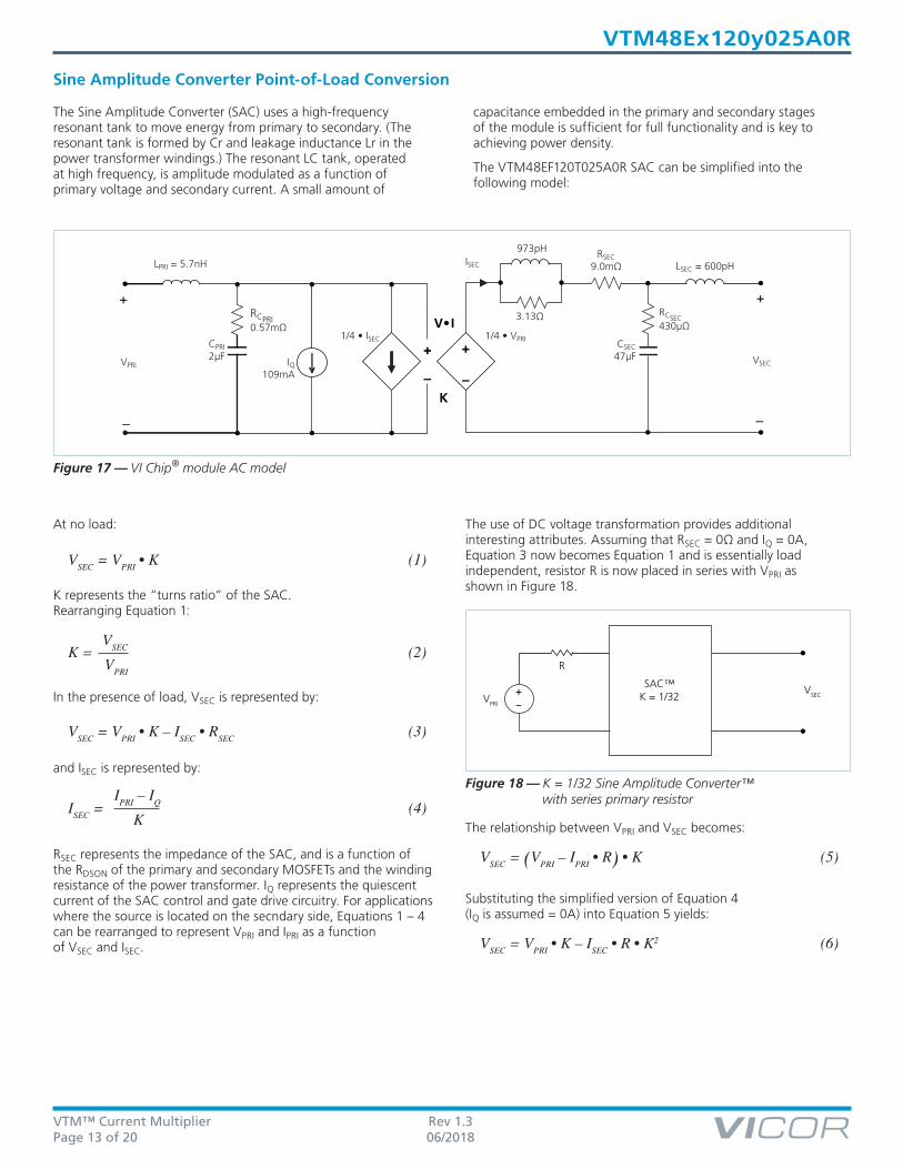
Sine Amplitude Converter Point-of-Load Conversion
The Sine Amplitude Converter (SAC) uses a high-frequency resonant tank to move energy from primary to secondary. (The resonant tank is formed by Cr and leakage inductance Lr in the power transformer windings.) The resonant LC tank, operated at high frequency, is amplitude modulated as a function of primary voltage and secondary current. A small amount of
capacitance embedded in the primary and secondary stages of the module is sufficient for full functionality and is key to achieving power density.
The VTM48EF120T025A0R SAC can be simplified into the following model:
Figure 17 — VI Chip® module AC model
+
–
+
–
VOUT
COUTVIN
V•I
K
+
–
+
–
CIN
IOUT
RCOUT
IQ
ROUT
RCIN
IQ109mA
1/4 • ISEC
RCPRI0.57mΩ
973pH
3.13Ω RCSEC430µΩ
LSEC = 600pHLPRI = 5.7nH ISECRSEC
9.0mΩ
VPRI VSEC
CSEC47µF
CPRI2µF
1/4 • VPRI
At no load:
K represents the “turns ratio” of the SAC. Rearranging Equation 1:
In the presence of load, VSEC is represented by:
and ISEC is represented by:
RSEC represents the impedance of the SAC, and is a function of the RDSON of the primary and secondary MOSFETs and the winding resistance of the power transformer. IQ represents the quiescent current of the SAC control and gate drive circuitry. For applications where the source is located on the secndary side, Equations 1 – 4 can be rearranged to represent VPRI and IPRI as a function of VSEC and ISEC.
The use of DC voltage transformation provides additional interesting attributes. Assuming that RSEC = 0Ω and IQ = 0A, Equation 3 now becomes Equation 1 and is essentially load independent, resistor R is now placed in series with VPRI as shown in Figure 18.
The relationship between VPRI and VSEC becomes:
Substituting the simplified version of Equation 4 (IQ is assumed = 0A) into Equation 5 yields:
Figure 18 — K = 1/32 Sine Amplitude Converter™ with series primary resistor
R
SAC™K = 1/32V
PRI
VSEC+
–
VSEC = VPRI • K (1)
K = VSEC
VPRI
(2)
VSEC = VPRI • K – ISEC • RSEC (3)
ISEC = IPRI – IQ
K(4)
VSEC = (VPRI – IPRI • R) • K (5)
VSEC = VPRI • K – ISEC • R • K2 (6)

VTM™ Current Multiplier Rev 1.3Page 14 of 20 06/2018
VTM48Ex120y025A0R
This is similar in form to Equation 3, where RSEC is used to represent the characteristic impedance of the SAC™. However, in this case a real R on the primary side of the SAC is effectively scaled by K2 with respect to the secondary.
Assuming that R = 1Ω, the effective R as seen from the secondary side is 0.98mΩ, with K = 1/32 as shown in Figure 18.
A similar exercise should be performed with the additon of a capacitor or shunt impedance at the primary to the SAC. A switch in series with VPRI is added to the circuit. This is depicted in Figure 19.
A change in VPRI with the switch closed would result in a change in capacitor current according to the following equation:
Assume that with the capacitor charged to VPRI, the switch is opened and the capacitor is discharged through the idealized SAC. In this case,
Substituting Equations 1 and 8 into Equation 7 reveals:
The equation in terms of the secondary has yielded a K2 scaling factor for C, specified in the denominator of the equation. A K factor less than unity results in an effectively larger capacitance on the secondary when expressed in terms of the primary. With a K = 1/32 as shown in Figure 19, C = 1µF would appear as C = 1024µF when viewed from the secondary. Note that in situations where the source voltage is located on the secondary side, the effect is reversed and effective valve of capacitance located on the secondary side is divided by a factor of 1/K2 when reflected to the primary.
Low impedance is a key requirement for powering a high-current, low-voltage load efficiently. A switching regulation stage should have minimal impedance while simultaneously providing appropriate filtering for any switched current. The use of a SAC between the regulation stage and the point-of-load provides a dual benefit of scaling down series impedance leading back to the source and scaling up shunt capacitance or energy storage as a function of its K factor squared. However, the benefits are not useful if the series impedance of the SAC is too high. The impedance of the SAC must be low, i.e., well beyond the crossover frequency of the system.
A solution for keeping the impedance of the SAC low involves switching at a high frequency. This enables small magnetic components because magnetizing currents remain low. Small magnetics mean small path lengths for turns. Use of low-loss core material at high frequencies also reduces core losses.
The two main terms of power loss in the VTM module are:
�� No load power dissipation (PNL): defined as the power used to power up the module with an enabled powertrain at no load.
�� Resistive loss (RSEC): refers to the power loss across the VTM modeled as pure resistive impedance.
Therefore,
The above relations can be combined to calculate the overall module efficiency:
C
S
SAC™K = 1/32V
PRI
VSEC+
–
Figure 19 — Sine Amplitude Converter™ with input capacitor
IC (t) = C dVPRI
dt(7)
IC = ISEC • K (8)
ISEC = (9)CK
2
dVSEC
dt•
PDISSIPATED = PNL + PRSEC(10)
PSEC = PPRI – PDISSIPATED = PPRI – PNL – PRSEC(11)
PSEC
PPRI
PPRI – PNL – PRSEC
PPRI
VPRI • IPRI – PNL – (ISEC)2 • RSEC
VPRI • IPRI
PNL + (ISEC)2 • RSEC
VPRI • IPRI
= 1 –
η =
=
= (12)
( )

VTM™ Current Multiplier Rev 1.3Page 15 of 20 06/2018
VTM48Ex120y025A0R
Primary and Secondary Filter Design
A major advantage of a SAC system versus a conventional PWM converter is that the former does not require large functional filters. The resonant LC tank, operated at extreme high frequency, is amplitude modulated as a function of primary voltage and secondary current and efficiently transfers charge through the isolation transformer. A small amount of capacitance embedded in the primary and secondary stages of the module is sufficient for full functionality and is key to achieving high power density.
This paradigm shift requires system design to carefully evaluate external filters in order to:
�� Guarantee low source impedance:
To take full advantage of the VTM module dynamic response, the impedance presented to its input terminals must be low from DC to approximately 5MHz. Primary capacitance may be added to improve transient performance or compensate for high source impedance.
�� Further reduce primary and/or secondary voltage ripple without sacrificing dynamic response:
Given the wide bandwidth of the VTM module, the source response is generally the limiting factor in the overall system response. Anomalies in the response of the source will appear at the secondary of the VTM module multiplied by its K factor.
�� Protect the module from overvoltage transients imposed by the system that would exceed maximum ratings and cause failures:
The VI Chip® module primary/secondary voltage ranges must not be exceeded. An internal overvoltage lockout function prevents operation outside of the normal operating primary or secondary range. Even during this condition, the powertrain is exposed to the applied voltage and power MOSFETs must withstand it.
Capacitive Filtering Considerations for a Sine Amplitude Converter™
It is important to consider the impact of adding capacitance to a Sine Amplitude Converter on the system as a whole. Both the capacitance value and the effective impedance of the capacitor must be considered.
A Sine Amplitude Converter has a DC RSEC value which has already been discussed on Page 13. The AC RSEC of the SAC contains several terms:
�� Resonant tank impedance
�� Primary lead inductance and internal capacitance
�� Secondary lead inductance and internal capacitance
The values of these terms are shown in the behavioral model on Page 13. It is important to note on which side of the transformer these impedances appear and how they reflect across the transformer given the K factor.
The overall AC impedance varies from model to model. For most models it is dominated by DC RSEC value from DC to beyond 500kHz. The behavioral model on Page 13 should be used to approximate the AC impedance of the specific model.
Any capacitors placed at the output of the VTM module reflect back to the primary of the module by the square of the K factor (Equation 9) with the impedance of the module appearing in series. It is very important to keep this in mind when using a PRM™ regulator to power the VTM module. Most PRM modules have a limit on the maximum amount of capacitance that can be applied to the secondary. This capacitance includes both the PRM output capacitance and the VTM module secondary capacitance reflected back to the primary. In PRM module remote-sense applications, it is important to consider the reflected value of VTM module secondary capacitance when designing and compensating the PRM module control loop.
Capacitance placed at the primary of the VTM module appear to the load reflected by the K factor with the impedance of the VTM module in series. In step-down ratios, the effective capacitance is increased by the K factor. The effective ESR of the capacitor is decreased by the square of the K factor, but the impedance of the module appears in series. Still, in most step-down VTM modules an electrolytic capacitor placed at the primary of the module will have a lower effective impedance compared to an electrolytic capacitor placed at the secondary. This is important to consider when placing capacitors at the secondary of the module. Even though the capacitor may be placed at the secondary, the majority of the AC current will be sourced from the lower impedance, which in most cases will be the module. This should be studied carefully in any system design using a module. In most cases, it should be clear that electrolytic secondary capacitors are not necessary to design a stable, well-bypassed system.

VTM™ Current Multiplier Rev 1.3Page 16 of 20 06/2018
VTM48Ex120y025A0R
Current Sharing
The SAC™ topology bases its performance on efficient transfer of energy through a transformer without the need of closed-loop control. For this reason, the transfer characteristic can be approximated by an ideal transformer with some resistive drop and positive temperature coefficient.
This type of characteristic is close to the impedance characteristic of a DC power distribution system, both in behavior (AC dynamic) and absolute value (DC dynamic).
When connected in an array with the same K factor, the VTM module will inherently share the load current (typically 5%) with parallel units according to the equivalent impedance divider that the system implements from the power source to the point-of-load.
Some general recommendations to achieve matched array impedances:
�� Dedicate common copper planes within the PCB to deliver and return the current to the modules.
�� Provide the PCB layout as symmetric as possible.
�� Apply same filtering to each unit.
For further details see: AN:016 Using BCM® Bus Converters in High Power Arrays.
Fuse Selection
In order to provide flexibility in configuring power systems VI Chip® products are not internally fused. Line fusing of VI Chip products is recommended at system level to provide thermal protection in case of catastrophic failure.
The fuse shall be selected by closely matching system requirements with the following characteristics:
�� Direction of power flow: if a power source is located on the primary, there must be a fuse located in the series with the primary source; if a source is located on the secondary, there must also be a fuse located in series with the secondary source.
�� Current rating (usually greater than maximum current of VTM module)
�� Maximum voltage rating (usually greater than the maximum possible primary voltage)
�� Ambient temperature
�� Nominal melting I2t
Bidirectional Operation
The VTM48EF120T025A0R is capable of bidirectional operation. If a voltage is present at the secondary which satisfies the condition VSEC > VPRI • K at the time the VC voltage is applied, or after the unit has started, then energy will be transferred from secondary to primary. The primary-to-secondary ratio will be maintained. The VTM48EF120T025A0R will continue to operate bidirectional as long as the primary and secondary are within the specified limits.
VPRI VSEC
+
– DC
ZPRI_EQ1
ZPRI_EQ2
ZSEC_EQ1
ZSEC_EQ2
Load
VTM 1RS_1
VTM 2RS_2
VTM nRS_n
ZSEC_EQnZPRI_EQn
Figure 20 — VTM module array

VTM™ Current Multiplier Rev 1.3Page 17 of 20 06/2018
VTM48Ex120y025A0R
inchmm
NOTES:
.
DIMENSIONS ARE .2. UNLESS OTHERWISE SPECIFIED, TOLERANCES ARE:
.X / [.XX] = +/-0.25 / [.01]; .XX / [.XXX] = +/-0.13 / [.005]3. PRODUCT MARKING ON TOP SURFACE
DXF and PDF files are available on vicorpower.com
4
inchmm .
DIMENSIONS ARE .2. UNLESS OTHERWISE SPECIFIED, TOLERANCES ARE:
.X / [.XX] = +/-0.25 / [.01]; .XX / [.XXX] = +/-0.13 / [.005]3. PRODUCT MARKING ON TOP SURFACE
DXF and PDF files are available on vicorpower.com
4
+PRI
-PRI-SEC2
-SEC1
+SEC2
+SEC1
J-Lead Package Recommended Land Pattern
J-Lead Package Mechanical Drawing
mm [inch]

VTM™ Current Multiplier Rev 1.3Page 18 of 20 06/2018
VTM48Ex120y025A0R
inchmm
NOTES:
.
DIMENSIONS ARE .2. UNLESS OTHERWISE SPECIFIED, TOLERANCES ARE:
.X / [.XX] = +/-0.25 / [.01]; .XX / [.XXX] = +/-0.13 / [.005]3. PRODUCT MARKING ON TOP SURFACE
DXF and PDF files are available on vicorpower.com
4
inchmm .
DIMENSIONS ARE .2. UNLESS OTHERWISE SPECIFIED, TOLERANCES ARE:
.X / [.XX] = +/-0.25 / [.01]; .XX / [.XXX] = +/-0.13 / [.005]3. PRODUCT MARKING ON TOP SURFACE
DXF and PDF files are available on vicorpower.com
4
+PRI
-PRI-SEC2
-SEC1
+SEC2
+SEC1
inchmm
NOTES:
.
DIMENSIONS ARE .2. UNLESS OTHERWISE SPECIFIED, TOLERANCES ARE:
.X / [.XX] = +/-0.25 / [.01]; .XX / [.XXX] = +/-0.13 / [.005]3. PRODUCT MARKING ON TOP SURFACE
DXF and PDF files are available on vicorpower.com
4
inchmm .
DIMENSIONS ARE .2. UNLESS OTHERWISE SPECIFIED, TOLERANCES ARE:
.X / [.XX] = +/-0.25 / [.01]; .XX / [.XXX] = +/-0.13 / [.005]3. PRODUCT MARKING ON TOP SURFACE
DXF and PDF files are available on vicorpower.com
4
+PRI
-PRI-SEC2
-SEC1
+SEC2
+SEC1
Through-Hole Package Recommended Land Pattern
Through-Hole Package Mechanical Drawing
mm [inch]

VTM™ Current Multiplier Rev 1.3Page 19 of 20 06/2018
VTM48Ex120y025A0R
Notes:
1. Maintain 3.50 (0.138) Dia. keep-out zone free of copper, all PCB layers.2. (A) Minimum recommended pitch is 39.50 (1.555). This provides 7.00 (0.275) component edge-to-edge spacing, and 0.50 (0.020) clearance between Vicor heat sinks. (B) Minimum recommended pitch is 41.00 (1.614). This provides 8.50 (0.334) component edge-to-edge spacing, and 2.00 (0.079) clearance between Vicor heat sinks.
3. VI Chip® module land pattern shown for reference only; actual land pattern may differ. Dimensions from edges of land pattern to push–pin holes will be the same for all full-size VI Chip® products.4. RoHS compliant per CST–0001 latest revision.
(NO GROUNDING CLIPS) (WITH GROUNDING CLIPS)
5. Unless otherwise specified: Dimensions are mm (inches) tolerances are: x.x (x.xx) = ±0.3 (0.01) x.xx (x.xxx) = ±0.13 (0.005)6. Plated through holes for grounding clips (33855) shown for reference, heat sink orientation and device pitch will dictate final grounding solution.
Recommended Heat Sink Push Pin Location
PC
VC
TM
Bottom View
A
B
C
D
E
F
G
H
J
K
L
M
N
P
R
T
4 3 2 1
A
B
C
D
E
H
J
K
L
M
N
P
R
T
+PRI
–PRI–SEC
–SEC
+SEC
+SEC
VTM Module Pin Configuration
Signal Name Pin Number
+PRI A1 – E1, A2 – E2
–PRI L1 – T1, L2 – T2
TM H1, H2
VC J1, J2
PC K1, K2
+SEC A3 – D3, A4 – D4, J3 – M3, J4 – M4
–SEC E3 – H3, E4 – H4, N3 – T3, N4 – T4

VTM™ Current Multiplier Rev 1.3Page 20 of 20 06/2018
VTM48Ex120y025A0R
Contact Us: http://www.vicorpower.com/contact-us
Vicor Corporation25 Frontage Road
Andover, MA, USA 01810Tel: 800-735-6200Fax: 978-475-6715
www.vicorpower.com
emailCustomer Service: [email protected]
Technical Support: [email protected]
Vicor’s comprehensive line of power solutions includes high density AC-DC and DC-DC modules and accessory components, fully configurable AC-DC and DC-DC power supplies, and complete custom power systems.
Information furnished by Vicor is believed to be accurate and reliable. However, no responsibility is assumed by Vicor for its use. Vicor makes no representations or warranties with respect to the accuracy or completeness of the contents of this publication. Vicor reserves the right to make changes to any products, specifications, and product descriptions at any time without notice. Information published by Vicor has been checked and is believed to be accurate at the time it was printed; however, Vicor assumes no responsibility for inaccuracies. Testing and other quality controls are used to the extent Vicor deems necessary to support Vicor’s product warranty. Except where mandated by government requirements, testing of all parameters of each product is not necessarily performed.
Specifications are subject to change without notice.
Visit http://www.vicorpower.com/dc-dc-converters-board-mount/vtm for the latest product information.
Vicor’s Standard Terms and Conditions and Product WarrantyAll sales are subject to Vicor’s Standard Terms and Conditions of Sale, and Product Warranty which are available on Vicor’s webpage (http://www.vicorpower.com/termsconditionswarranty) or upon request.
Life Support Policy
VICOR’S PRODUCTS ARE NOT AUTHORIZED FOR USE AS CRITICAL COMPONENTS IN LIFE SUPPORT DEVICES OR SYSTEMS WITHOUT THE EXPRESS PRIOR WRITTEN APPROVAL OF THE CHIEF EXECUTIVE OFFICER AND GENERAL COUNSEL OF VICOR CORPORATION. As used herein, life support devices or systems are devices which (a) are intended for surgical implant into the body, or (b) support or sustain life and whose failure to perform when properly used in accordance with instructions for use provided in the labeling can be reasonably expected to result in a significant injury to the user. A critical component is any component in a life support device or system whose failure to perform can be reasonably expected to cause the failure of the life support device or system or to affect its safety or effectiveness. Per Vicor Terms and Conditions of Sale, the user of Vicor products and components in life support applications assumes all risks of such use and indemnifies Vicor against all liability and damages.
Intellectual Property Notice
Vicor and its subsidiaries own Intellectual Property (including issued U.S. and Foreign Patents and pending patent applications) relating to the products described in this data sheet. No license, whether express, implied, or arising by estoppel or otherwise, to any intellectual property rights is granted by this document. Interested parties should contact Vicor’s Intellectual Property Department.
The products described on this data sheet are protected by the following U.S. Patents Numbers: 5,945,130; 6,403,009; 6,710,257; 6,911,848; 6,930,893; 6,934,166; 6,940,013; 6,969,909; 7,038,917; 7,145,186; 7,166,898; 7,187,263; 7,202,646; 7,361,844; D496,906; D505,114; D506,438; D509,472; and for use under 6,975,098 and 6,984,965.
©2018 Vicor Corporation. All rights reserved. The Vicor name is a registered trademark of Vicor Corporation.All other trademarks, product names, logos and brands are property of their respective owners.