Embed Size (px)
Citation preview
8/6/2019 xilinx pwm
http://slidepdf.com/reader/full/xilinx-pwm 1/7
8/6/2019 xilinx pwm
http://slidepdf.com/reader/full/xilinx-pwm 2/7
Online at http://ejum.fsktm.um.edu.myVol.1, No 2 December 2006 pp 40-45 © 2006 Engineering e-Transaction, University of Malaya
_______________________________________________________________________________________________
converted in configuration data file and loaded intoXS95108 CPLD board.
II. THE PROPOSED CIRCUIT
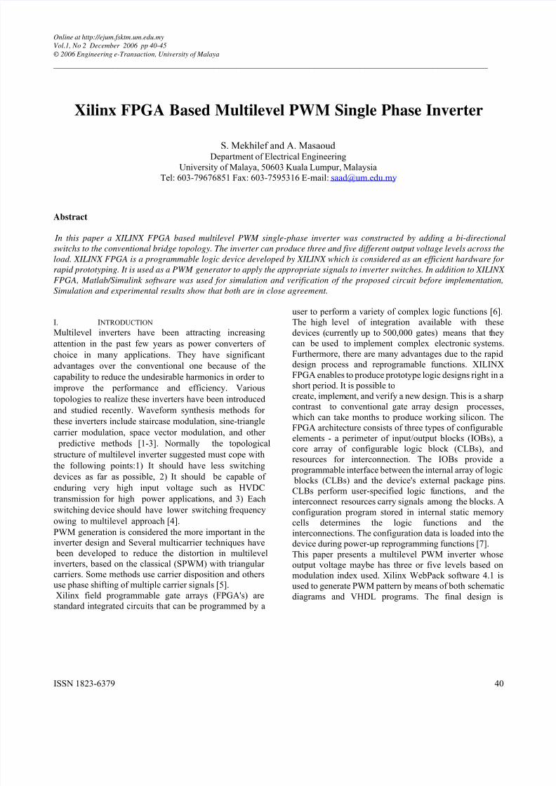
The multilevel PWM single phase inverter has been clearly presented in Fig.1. A bi-directional switch consists of twoswitches S5 and S6 and four diodes are added to theconventional full-bridge inverter.
Fig.1 The proposed circuit of the multilevel PWM single phase inverter
Fig.2 PWM generation technique used for the multilevelPWM single phase inverter.
Two dc capacitors, which are considered as an energy tank for the inverter, are also connected to the dc voltagesource. The function of bi-directional switch is to controlcurrent flow. The PWM pattern adopted in the proposedinverter makes the inverter producing output voltage withthree levels (zero and half supply dc voltage positive andnegative respectively) at modulation index (Ma ≤ 0.5) andfive levels (zero, half and full supply voltage positive andnegative respectively) at modulation index (Ma > 0.5).The parameters of the modulation process are shown inFig.2 and defined as following:
1) The modulation index is defined as:
2AcAm
Ma = (1)
Where Am is peak value of sinusoidal wave and Ac is the peak is the carrier peak-peak value.
2) The frequency modulation index:
fm fc=Mf (2)
Where is the frequency of the carrier wave and isthe frequency of the sinusoidal wave.
fc fm
3) The angle of displacement existing between thesinusoidal wave and the first positive carrier wave can bedefined as following:
Ac1)(Am.Sin =φ
⎟ ⎠ ⎞
⎜⎝ ⎛ =
AmAc
Sin1 1-φ (3)
12 φ π φ −= (4)
13 φ π φ += (5)
124 φ π φ −= (6)The proposed inverter may be operate in four modesdefined as following:Mode1: 21 φ φ << wt (7)
Mode2: 10 φ ≤< wt and π φ ≤< wt 2 (8)
Mode3: 3φ π ≤< wt and π φ 24 ≤< wt (9)
Mode4: 43 φ φ ≤< wt (10)At modulation index Ma > 0.5 the inverter operates in allmodes producing five voltage levels 0, Vdc/2,Vdc, -Vdc/2,-Vdc respectively.At certain load when the required voltage is Vdc/2 or less
the inverter operates at modulation index Ma ≤ 0.5 in twomodes 2 and 3 only. The displacement angles become:
221
π φ φ == (11)
23
43π
φ φ == (12)
ONSWITCHES
Va Vb Vab=Vo
S4,S1 Vdc 0 +VdcS4,S6 Vdc/2 0 +Vdc/2S4,S3 0 0 0S2,S1 Vdc/2 Vdc/2 0
S2, S5 0 Vdc -VdcS2,S3 0 Vdc/2 -Vdc/2
Table.1 Output voltage based on switches combination
ISSN 1823-6379 41

8/6/2019 xilinx pwm
http://slidepdf.com/reader/full/xilinx-pwm 3/7
Online at http://ejum.fsktm.um.edu.myVol.1, No 2 December 2006 pp 40-45 © 2006 Engineering e-Transaction, University of Malaya
_______________________________________________________________________________________________
Fig.3 The block diagram of PWM generation strategy
Fig.4 The block diagram of single phase PWM generator in XILINX FPGA
III. PWM GENERATION USING XILINX FPGA
The overall block diagram of the proposed multilevelsingle-phase inverter PWM generator is shown in Fig.3.The upper and lower carrier waves (1800 Hz) are
compared with the sinusoidal wave (50 Hz). In same time a pulse signal has frequency of (50 Hz) is generated andinverted to get its inverse pulse signal.
Fig.5 Single phase PWM scheme generator in XILINXFPGA
There are only three control signals S6, S5 and S2 will be needed to derive, another three S3, S1, and S4 aresimply generated in method of the logical inverse of S6,S5, and S2 respectively as shown in fig.5.
1- sinusoidal wave generationThe schematic diagram of the sine wave consists of amemory Pointer unit and schematic block includes aVHDL program for sine wave data as shown in Fig.4. TheVHDL program includes 19 sine wave data calculated at
every 5° degrees, these data cover quarter cycle of sinewave 90° degrees. As the modulation index depends on the modulation waveamplitude, the sine wave data can be changed to achievethe required modulation index and thus the required outputvoltage.
2- Carrier wave generationAn 8-bit up-down counter is clocked at 918 KHz to
produce 1800Hz carrier frequency and VHDL programincludes a simple addition process is also written andconverted into schematic block (addition unit) to generatetwo types of carrier (upper and lower) waves. The main
clock frequency is determined by the following formula:
( )212 −= n fc fclk (12)
Where is the main clock frequency, is the carrier (upper and lower) wave frequencies and n is the bit size of the up-down counter.
fclk fc
ISSN 1823-6379 42

8/6/2019 xilinx pwm
http://slidepdf.com/reader/full/xilinx-pwm 4/7
Online at http://ejum.fsktm.um.edu.myVol.1, No 2 December 2006 pp 40-45 © 2006 Engineering e-Transaction, University of Malaya
_______________________________________________________________________________________________
3- Pulse signal 50Hz generationTwo inverse pulse signals have same frequency (50Hz)need to be generated; their frequencies are similar to thesinusoidal wave and the output frequency.
Pointer unit consists of an 8 bit counter, some logic gatesand VHDL program developed to store data in term of condition statements are the main structure of the pulsesignal (50 Hz). These two signals have two functions, firstas a switching signal for switches S4 and S2, second toinvolve with the resultant signals produced fromcomparators to generate the appropriate switching signalsfor switches S6, S3, S5 and S1.
4- PWM distribution unitThis unit is used to distribute the PWM output pattern tothe switches (S1, S2, S3, S4, S5 and S4). The distributionunit consists of a few logic gates (AND, OR, and NOT)
deal with the three main signals produced fromcomparators and pulse signals 50 Hz generation unit toform the final PWM as shown in Fig.5.
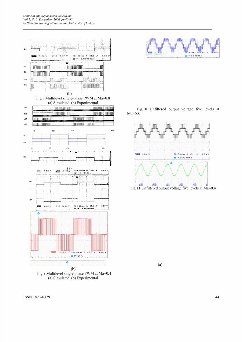
SIMULATION AND EXPERMINTAL RESULTS
The model of the proposed multilevel PWM single phaseinverter is simulated by using Matlab/Simulink®simulation tool. The PWM pattern is derived and simulatedat different modulation indexes (Ma) as a control signals;the system is tested and simulated by different types of load, resistive, and mixed (resistive and inductive) loads
respectively. The waveforms of voltage output and loadcurrent are obtained, experimental and simulated resultsare compared and show satisfactory results.
Fig.6 Multilevel PWM single phase simulation results using XILINXFPGA at Ma = 0.8.
Fig.7 Multilevel PWM single phase simulation results using XILINX
FPGA at Ma = 0.4.
(a)
ISSN 1823-6379 43
8/6/2019 xilinx pwm
http://slidepdf.com/reader/full/xilinx-pwm 5/7

8/6/2019 xilinx pwm
http://slidepdf.com/reader/full/xilinx-pwm 6/7
Online at http://ejum.fsktm.um.edu.myVol.1, No 2 December 2006 pp 40-45 © 2006 Engineering e-Transaction, University of Malaya
_______________________________________________________________________________________________
(b)Fig.12 Ac voltage waveform before and after the filter inthe proposed multilevel PWM inverter at modulationindexes (a) 0.8 and (b) 0.4.
Fig.13 Ac voltage and current output waveforms for resistive load.
Fig.14 Ac voltage and current output waveforms for (resistive- inductive) load.
Fig.15 Ac voltage output harmonic spectral after filter
IV. CONCLUSION
The switching patterns adopted are applied at the sixinverter switches to generate five or three output voltagelevels at different modulation indexes. XILINX FPGAenables to make easy, fast and flexible design andimplementation. The experimental and simulated resultsare show satisfactory results in term of total harmonicdistortion and output voltage and current waveformshapes.
REFERENCES
[1] V.G.Agelidis, D.M.Baker, W.B.Lawrance and C.V. Nayar “ AMultilevel PWM Inverter Topology for Photovoltaic Applications”
IEEE.ISIE’97, Guimar ä es, Portugal, pp.589-594,1997.
[2] J.S. Lai and F.Z.Peng, ”Multilevel converters –Anew breed of power conversion ” IEEE Trans. 1nd.
Applicat ., vol.32, pp. 509-517, May/June. 1996.[3] N.S. Choi, J.H. Cho, and G.H. Cho, “A General
circuit Topology of Multilevel Inverter” IEEE Trans . Power Electronics , vol. 6, pp.96-103, 1991.
[4] E. Cengelci, S. U. Sulistijo, B. O. Woom, P. Enjeti, R.Teodorescu, and F. Blaabjerge,“A new mediumvoltage PWM inverter topology for adjustable speeddrives” in Conf. Rec. IEEE-IAS Annu. Meeting , St.
Louis MO, pp.1416-1423, Oct.1998.[5] B. N. Mwinyiwiwa, Z.Wolanski, and B. T. Ooi,
“Microp- rocessor implemented SPWM for multiconverters with phase-shifted triangle carriers”in Conf. Rec IEEE-IAS Annu. Meet- ing ,
NewOrleans, pp. 1542–1549, Oct. 1997.[6] S.Mekhilef and N.A.Rahim,”XILINX FPGA
three-phase PWM inverter and its application for utility connected PV system”inProc.IEEE.TENCO’02 , 2002, pp.2079-2082.
ISSN 1823-6379 45

8/6/2019 xilinx pwm
http://slidepdf.com/reader/full/xilinx-pwm 7/7
Online at http://ejum.fsktm.um.edu.myVol.1, No 2 December 2006 pp 40-45 © 2006 Engineering e-Transaction, University of Malaya
_______________________________________________________________________________________________
[7] Introduction to WebPack 4.1 for CPLDs, XESSCorporation, 2001.
ISSN 1823-6379 46