Embed Size (px)
Citation preview
15 • 2019 IEEE International Solid-State Circuits Conference
ISSCC 2019 / SESSION 14 / MACHINE LEARNING & DIGITAL LDO CIRCUITS / 14.5
14.5 A 0.6-to-1.1V Computationally Regulated Digital LDO with 2.79-Cycle Mean Settling Time and Autonomous Runtime Gain Tracking in 65nm CMOS
Xun Sun, Akshat Boora, Wenbing Zhang, Venkata Rajesh Pamula, Visvesh Sathe
University of Washington, Seattle, WA
Low-Dropout Regulators (LDOs) play an important role in enabling fine-grainedsupply-voltage domains for energy-efficient SoC design [1]. Digital LDOs are ofparticular interest due to integration and scalability advantages, but their transientresponse is slowed down by intrinsic limitations in sampled feedback systems.Design margins to ensure stability across worst-case PVT conditions furtherdegrade transient response. Meanwhile, voltage domains continue to shrink insize, thus mandating a faster LDO response to compensate for reduced availabledecoupling capacitance (decap).
Recently reported non-linear control and event-driven architectures offer fastrecovery times [2] [3]. However, non-linear approaches face the challenge ofensuring stable mode transitions under random load current (IL) conditions.Event-driven LDOs trigger logic to control MOS devices based on thresholdcrossings made by the regulated voltage (Vout). However, typical digital systemsexhibit constant load fluctuation, which can result in prohibitive switching losses.To address the impact of worst-case margining, adaptive LDO designs have alsobeen proposed, but they largely focus on suppressing Vout ripple [4], andcompensating for load current variation [5].
This paper presents computational regulation, a technique for fast and stabletransient response across PVT. This concept is demonstrated in a Digital LDOthat drives a Cortex-M0 processor with an integrated linear algebra accelerator(Fig. 14.5.1). The key idea is to: 1) derive time-domain models that are moreaccurate than those obtained from the traditional discrete-time transfer functionand 2) evaluate the resulting state equations at runtime for rapid regulatorresponse. We also introduce Autonomous Gain Tracking (AGT), a low-overhead,low-complexity technique that examines Vout statistics for runtime loop-gaintuning to enable rapid LDO response across PVT. In any cycle n, the LDO samplesand quantizes the error voltage ΔV[n] = Vout[n] - Vref. A Solver then uses ΔV[n] toevaluate LDO state equations to determine k[n], the number of PMOS devices tobe turned-on in the same cycle. Ideally, k[n] is selected to meet IL requirementsand restore Vout within one LDO cycle. To determine k[n], the Solver requires awell-tuned gain term, GS = CL/(I0T) (Fig. 14.5.1) that captures important designparameters. These parameters include: 1) I0, the current delivered by a unit LDOPMOS device, 2) CL, the Vout decap, and 3) T, the LDO clock period. GS is thereforesensitive to PVT variation and must be tracked for rapid, robust response. AGTmonitors the LDO loop gain and subsequently adjusts GS to maintain speed andstability.
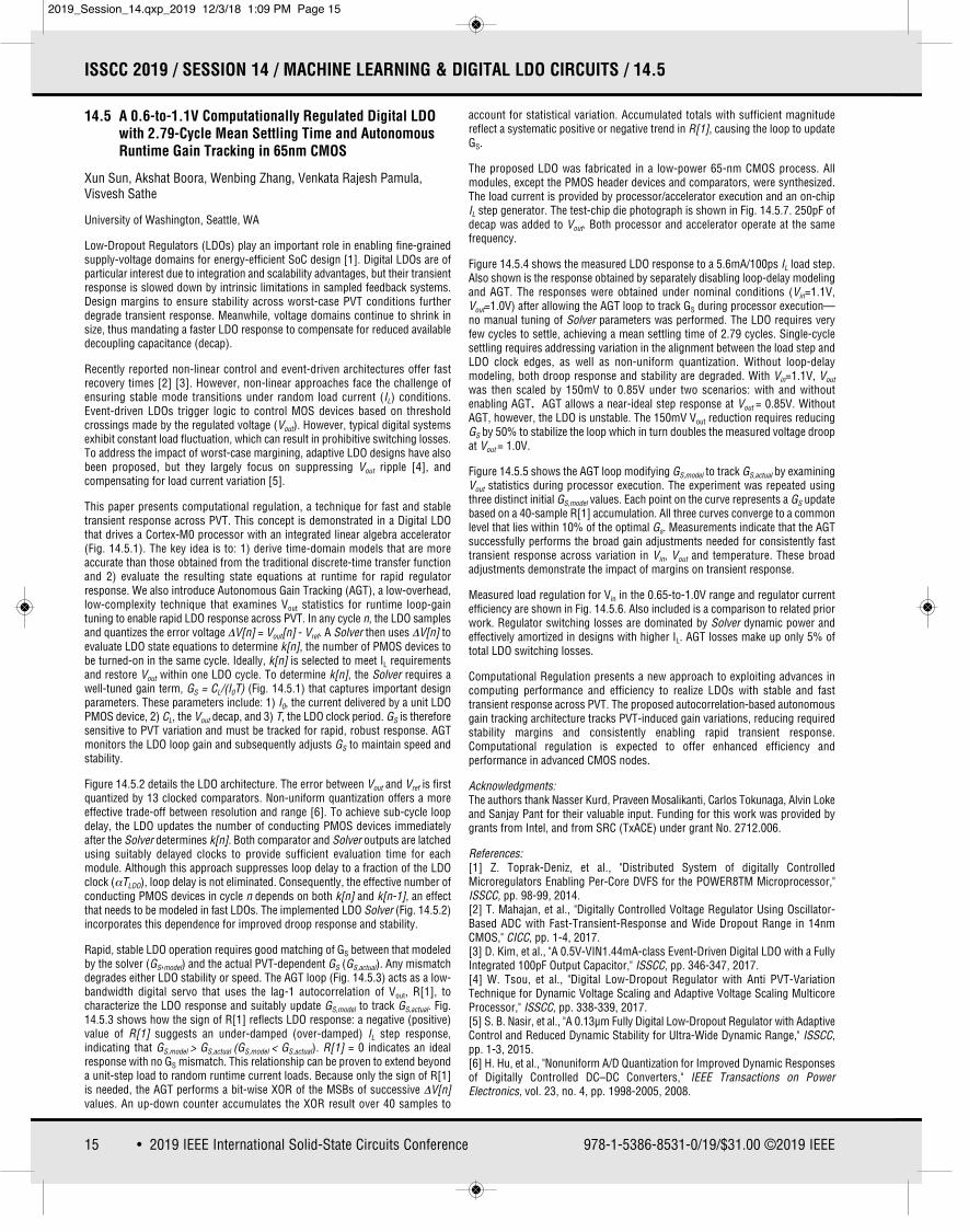
Figure 14.5.2 details the LDO architecture. The error between Vout and Vref is firstquantized by 13 clocked comparators. Non-uniform quantization offers a moreeffective trade-off between resolution and range [6]. To achieve sub-cycle loopdelay, the LDO updates the number of conducting PMOS devices immediatelyafter the Solver determines k[n]. Both comparator and Solver outputs are latchedusing suitably delayed clocks to provide sufficient evaluation time for eachmodule. Although this approach suppresses loop delay to a fraction of the LDOclock (αTLDO), loop delay is not eliminated. Consequently, the effective number ofconducting PMOS devices in cycle n depends on both k[n] and k[n-1], an effectthat needs to be modeled in fast LDOs. The implemented LDO Solver (Fig. 14.5.2)incorporates this dependence for improved droop response and stability.
Rapid, stable LDO operation requires good matching of GS between that modeledby the solver (GS,model) and the actual PVT-dependent GS (GS,actual). Any mismatchdegrades either LDO stability or speed. The AGT loop (Fig. 14.5.3) acts as a low-bandwidth digital servo that uses the lag-1 autocorrelation of Vout, R[1], tocharacterize the LDO response and suitably update GS,model to track GS,actual. Fig.14.5.3 shows how the sign of R[1] reflects LDO response: a negative (positive)value of R[1] suggests an under-damped (over-damped) IL step response,indicating that GS,model > GS,actual (GS,model < GS,actual). R[1] = 0 indicates an idealresponse with no GS mismatch. This relationship can be proven to extend beyonda unit-step load to random runtime current loads. Because only the sign of R[1]is needed, the AGT performs a bit-wise XOR of the MSBs of successive ΔV[n]values. An up-down counter accumulates the XOR result over 40 samples to
account for statistical variation. Accumulated totals with sufficient magnitudereflect a systematic positive or negative trend in R[1], causing the loop to updateGS.
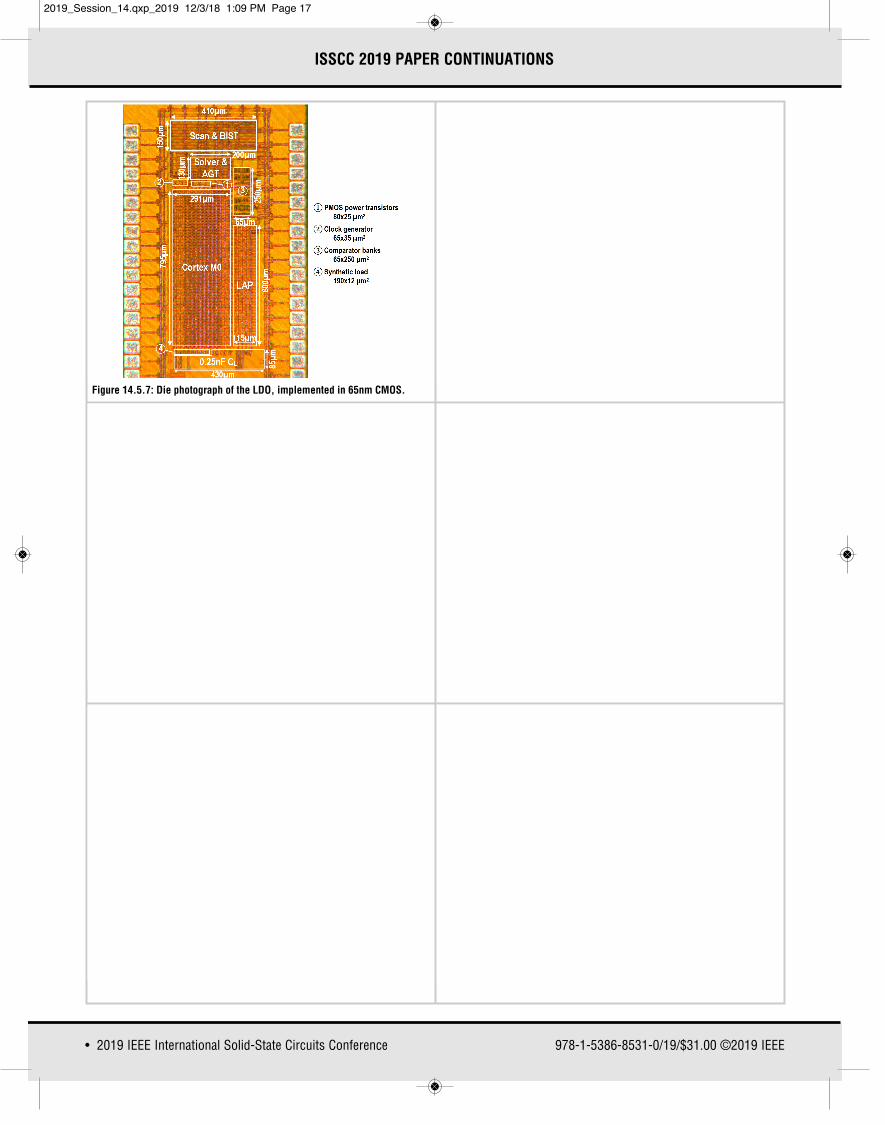
The proposed LDO was fabricated in a low-power 65-nm CMOS process. Allmodules, except the PMOS header devices and comparators, were synthesized.The load current is provided by processor/accelerator execution and an on-chipIL step generator. The test-chip die photograph is shown in Fig. 14.5.7. 250pF ofdecap was added to Vout. Both processor and accelerator operate at the samefrequency.
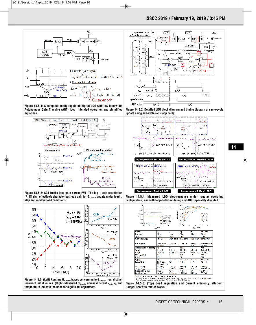
Figure 14.5.4 shows the measured LDO response to a 5.6mA/100ps IL load step.Also shown is the response obtained by separately disabling loop-delay modelingand AGT. The responses were obtained under nominal conditions (Vin=1.1V,Vout=1.0V) after allowing the AGT loop to track GS during processor execution—no manual tuning of Solver parameters was performed. The LDO requires veryfew cycles to settle, achieving a mean settling time of 2.79 cycles. Single-cyclesettling requires addressing variation in the alignment between the load step andLDO clock edges, as well as non-uniform quantization. Without loop-delaymodeling, both droop response and stability are degraded. With Vin=1.1V, Voutwas then scaled by 150mV to 0.85V under two scenarios: with and withoutenabling AGT. AGT allows a near-ideal step response at Vout = 0.85V. WithoutAGT, however, the LDO is unstable. The 150mV Vout reduction requires reducingGS by 50% to stabilize the loop which in turn doubles the measured voltage droopat Vout = 1.0V.
Figure 14.5.5 shows the AGT loop modifying GS,model to track GS,actual by examiningVout statistics during processor execution. The experiment was repeated usingthree distinct initial GS,model values. Each point on the curve represents a GS updatebased on a 40-sample R[1] accumulation. All three curves converge to a commonlevel that lies within 10% of the optimal Gs. Measurements indicate that the AGTsuccessfully performs the broad gain adjustments needed for consistently fasttransient response across variation in Vin, Vout and temperature. These broadadjustments demonstrate the impact of margins on transient response.
Measured load regulation for Vin in the 0.65-to-1.0V range and regulator currentefficiency are shown in Fig. 14.5.6. Also included is a comparison to related priorwork. Regulator switching losses are dominated by Solver dynamic power andeffectively amortized in designs with higher IL. AGT losses make up only 5% oftotal LDO switching losses.
Computational Regulation presents a new approach to exploiting advances incomputing performance and efficiency to realize LDOs with stable and fasttransient response across PVT. The proposed autocorrelation-based autonomousgain tracking architecture tracks PVT-induced gain variations, reducing requiredstability margins and consistently enabling rapid transient response.Computational regulation is expected to offer enhanced efficiency andperformance in advanced CMOS nodes.
Acknowledgments:The authors thank Nasser Kurd, Praveen Mosalikanti, Carlos Tokunaga, Alvin Lokeand Sanjay Pant for their valuable input. Funding for this work was provided bygrants from Intel, and from SRC (TxACE) under grant No. 2712.006.
References:[1] Z. Toprak-Deniz, et al., "Distributed System of digitally ControlledMicroregulators Enabling Per-Core DVFS for the POWER8TM Microprocessor,"ISSCC, pp. 98-99, 2014.[2] T. Mahajan, et al., "Digitally Controlled Voltage Regulator Using Oscillator-Based ADC with Fast-Transient-Response and Wide Dropout Range in 14nmCMOS," CICC, pp. 1-4, 2017.[3] D. Kim, et al., "A 0.5V-VIN1.44mA-class Event-Driven Digital LDO with a FullyIntegrated 100pF Output Capacitor," ISSCC, pp. 346-347, 2017.[4] W. Tsou, et al., "Digital Low-Dropout Regulator with Anti PVT-VariationTechnique for Dynamic Voltage Scaling and Adaptive Voltage Scaling MulticoreProcessor," ISSCC, pp. 338-339, 2017.[5] S. B. Nasir, et al., "A 0.13μm Fully Digital Low-Dropout Regulator with AdaptiveControl and Reduced Dynamic Stability for Ultra-Wide Dynamic Range," ISSCC,pp. 1-3, 2015.[6] H. Hu, et al., "Nonuniform A/D Quantization for Improved Dynamic Responsesof Digitally Controlled DC–DC Converters," IEEE Transactions on PowerElectronics, vol. 23, no. 4, pp. 1998-2005, 2008.
978-1-5386-8531-0/19/$31.00 ©2019 IEEE
2019_Session_14.qxp_2019 12/3/18 1:09 PM Page 15
16DIGEST OF TECHNICAL PAPERS •
ISSCC 2019 / February 19, 2019 / 3:45 PM
Figure 14.5.1: A computationally regulated digital LDO with low-bandwidthAutonomous Gain Tracking (AGT) loop. Intended operation and simplifiedequations.
Figure 14.5.2: Detailed LDO block diagram and timing diagram of same-cycleupdate using sub-cycle (αT) loop delay.
Figure 14.5.3: AGT tracks loop gain across PVT. The lag-1 auto-correlation(R[1]) sign effectively characterizes loop gain for GS,model update under load IL
step and random load conditions.
Figure 14.5.5: (Left) Runtime GS,model traces converging to GS,actual from distinctincorrect initial values. (Right) Measured GS,model across different Vout, Vin andtemperature indicate the need for significant adjustment.
Figure 14.5.6: (Top) Load regulation and Current efficiency. (Bottom)Comparison with related works.
Figure 14.5.4: Measured LDO step-response under regular operatingconfiguration, and with loop-delay modeling and AGT separately disabled.
14
2019_Session_14.qxp_2019 12/3/18 1:09 PM Page 16
• 2019 IEEE International Solid-State Circuits Conference 978-1-5386-8531-0/19/$31.00 ©2019 IEEE
ISSCC 2019 PAPER CONTINUATIONS
Figure 14.5.7: Die photograph of the LDO, implemented in 65nm CMOS.
2019_Session_14.qxp_2019 12/3/18 1:09 PM Page 17


![WES-XUN I 카다로그.ppt [호환 모드] WES-XUN I WESnet-eXtendableUbiquitous Network I 8051 AVR PIC 사양서 분류 구분 사양 MCU 8051 89S52 AVR ATmega128(AT90CAN128) PIC](https://img.pdfslide.tips/doc/110x75/5ff95c91de84c221fd4fa061/wes-xun-i-eeoeeppt-eeoe-wes-xun-i-wesnet-extendableubiquitous.jpg)