Embed Size (px)
Citation preview

深入了解抖动与高速串行测试
Yu Ocean
2014.5
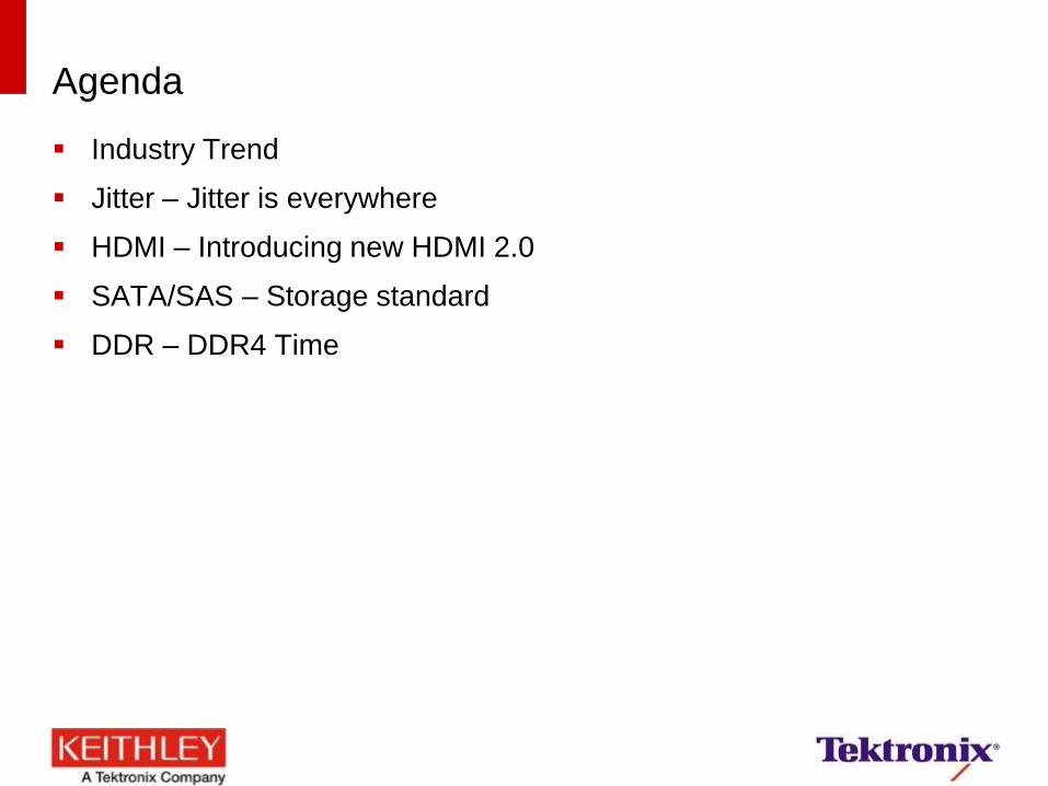
Agenda
Industry Trend
Jitter – Jitter is everywhere
HDMI – Introducing new HDMI 2.0
SATA/SAS – Storage standard
DDR – DDR4 Time
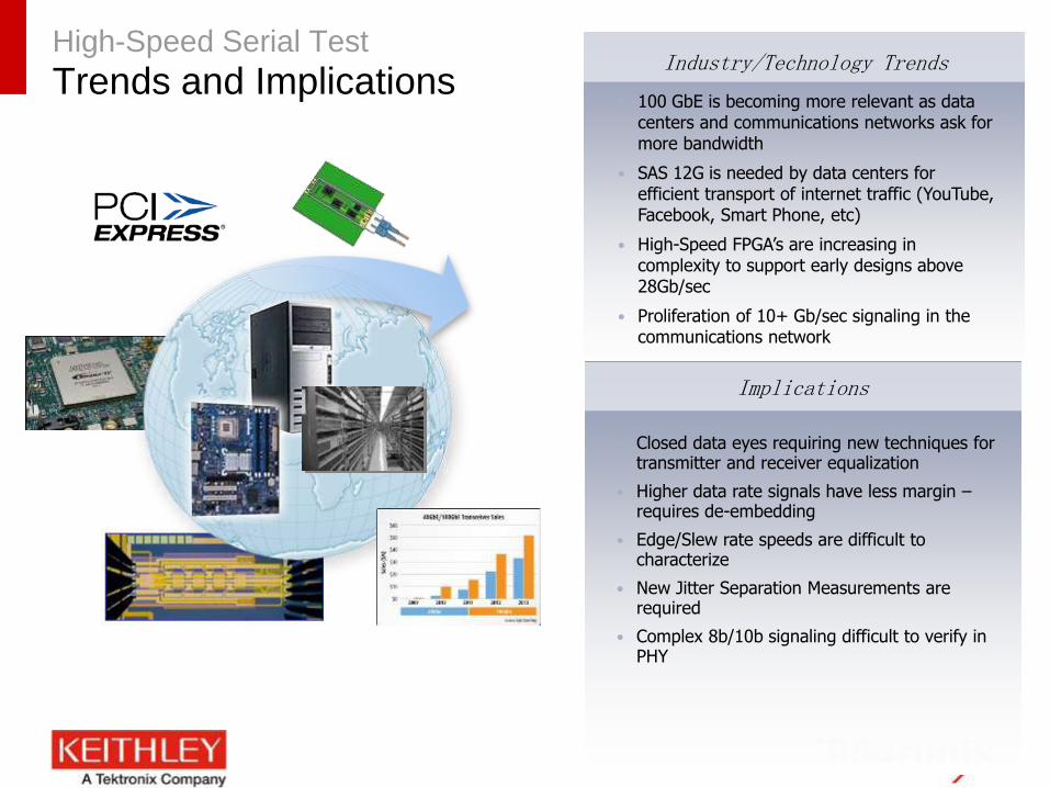
High-Speed Serial Test
Trends and Implications • 100 GbE is becoming more relevant as data
centers and communications networks ask for more bandwidth
• SAS 12G is needed by data centers for efficient transport of internet traffic (YouTube, Facebook, Smart Phone, etc)
• High-Speed FPGA’s are increasing in complexity to support early designs above 28Gb/sec
• Proliferation of 10+ Gb/sec signaling in the communications network
Industry/Technology Trends
• Closed data eyes requiring new techniques for transmitter and receiver equalization
• Higher data rate signals have less margin – requires de-embedding
• Edge/Slew rate speeds are difficult to characterize
• New Jitter Separation Measurements are required
• Complex 8b/10b signaling difficult to verify in PHY
Implications
Jitter – Jitter is everywhere
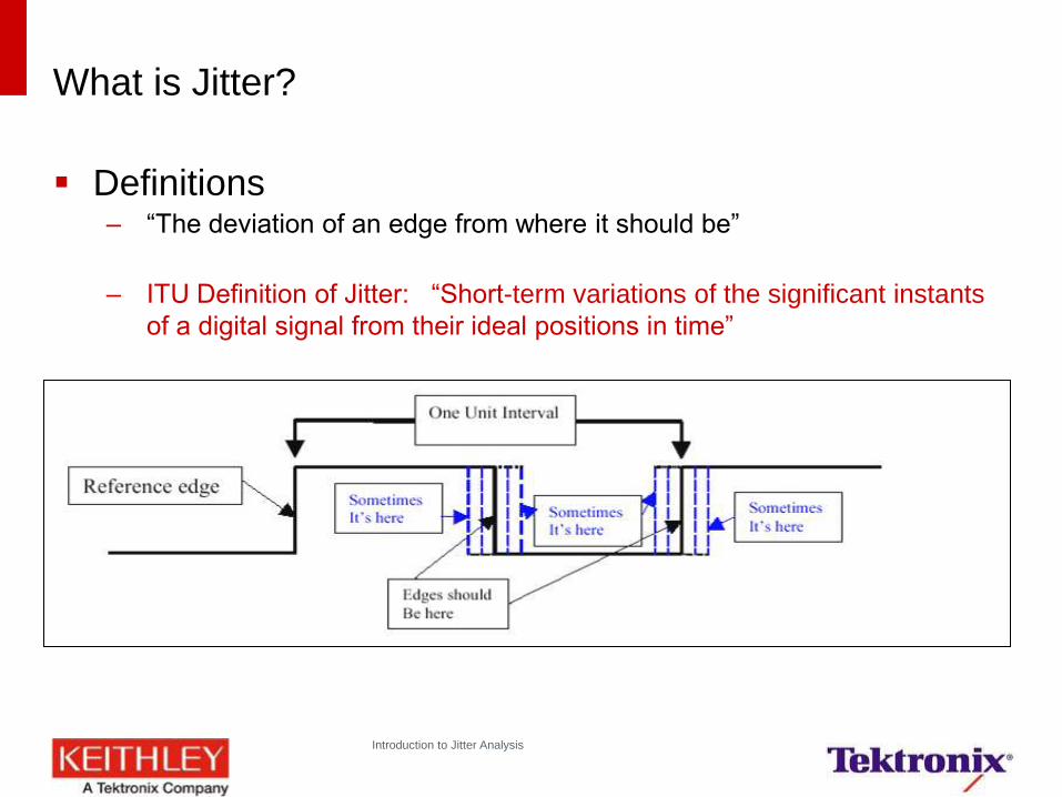
What is Jitter?
Definitions – “The deviation of an edge from where it should be”
– ITU Definition of Jitter: “Short-term variations of the significant instants
of a digital signal from their ideal positions in time”
Introduction to Jitter Analysis
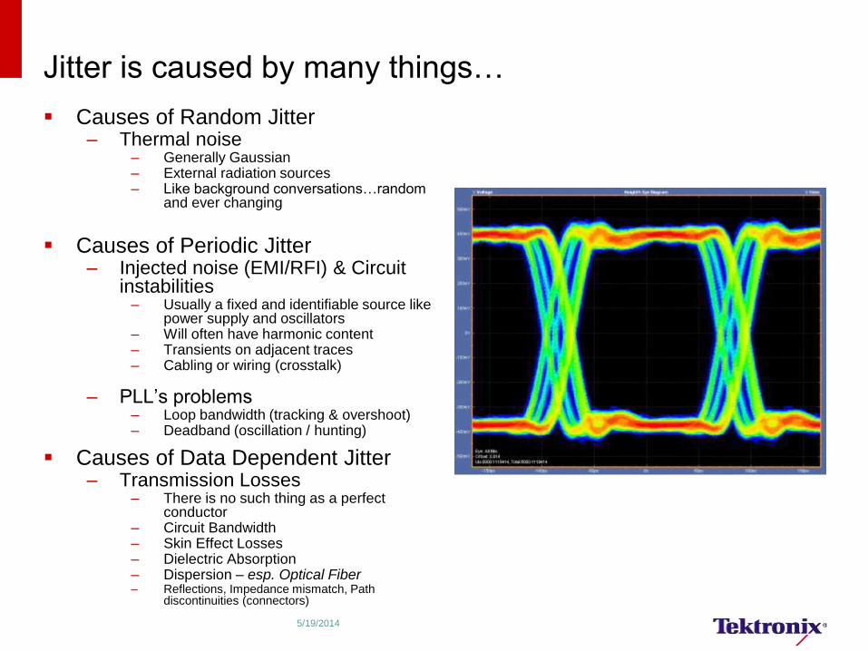
Jitter is caused by many things…
Causes of Random Jitter – Thermal noise
– Generally Gaussian – External radiation sources – Like background conversations…random
and ever changing
Causes of Periodic Jitter – Injected noise (EMI/RFI) & Circuit
instabilities – Usually a fixed and identifiable source like
power supply and oscillators – Will often have harmonic content – Transients on adjacent traces – Cabling or wiring (crosstalk)
– PLL’s problems – Loop bandwidth (tracking & overshoot) – Deadband (oscillation / hunting)
Causes of Data Dependent Jitter – Transmission Losses
– There is no such thing as a perfect conductor
– Circuit Bandwidth – Skin Effect Losses – Dielectric Absorption – Dispersion – esp. Optical Fiber – Reflections, Impedance mismatch, Path
discontinuities (connectors)
5/19/2014
Types of Jitter
5/19/2014 Introduction to Jitter Analysis
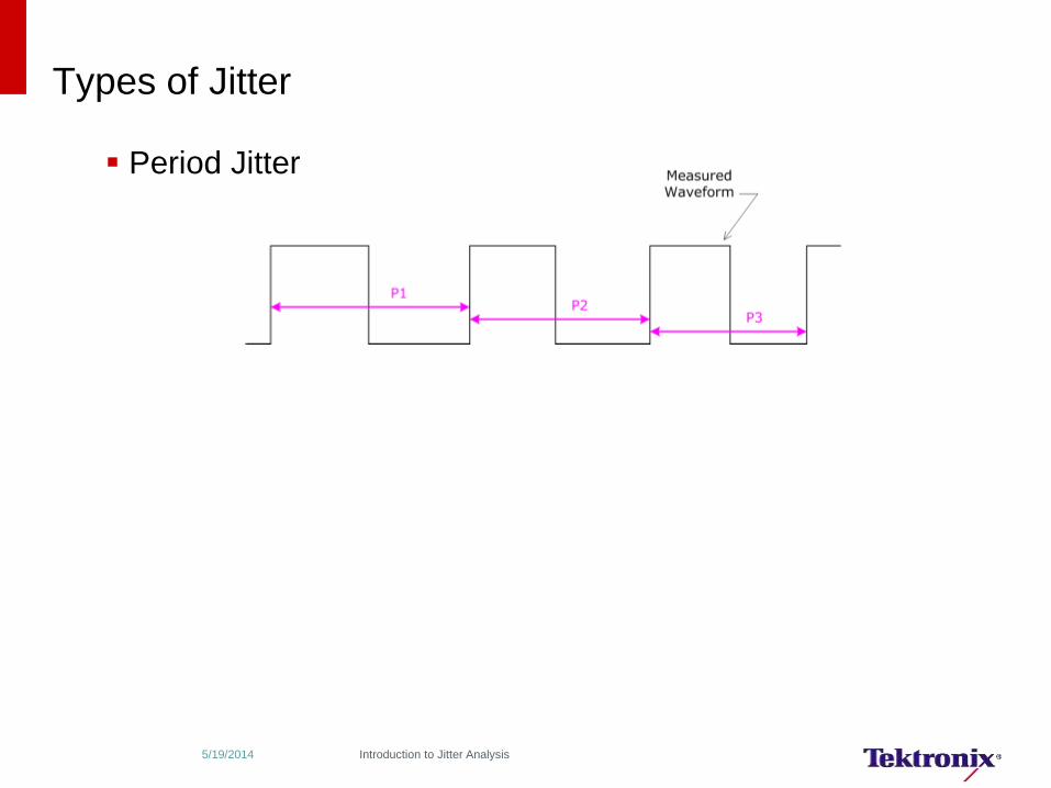
Period Jitter
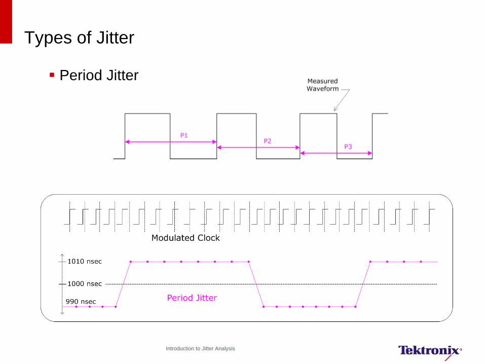
Types of Jitter
Introduction to Jitter Analysis
Period Jitter
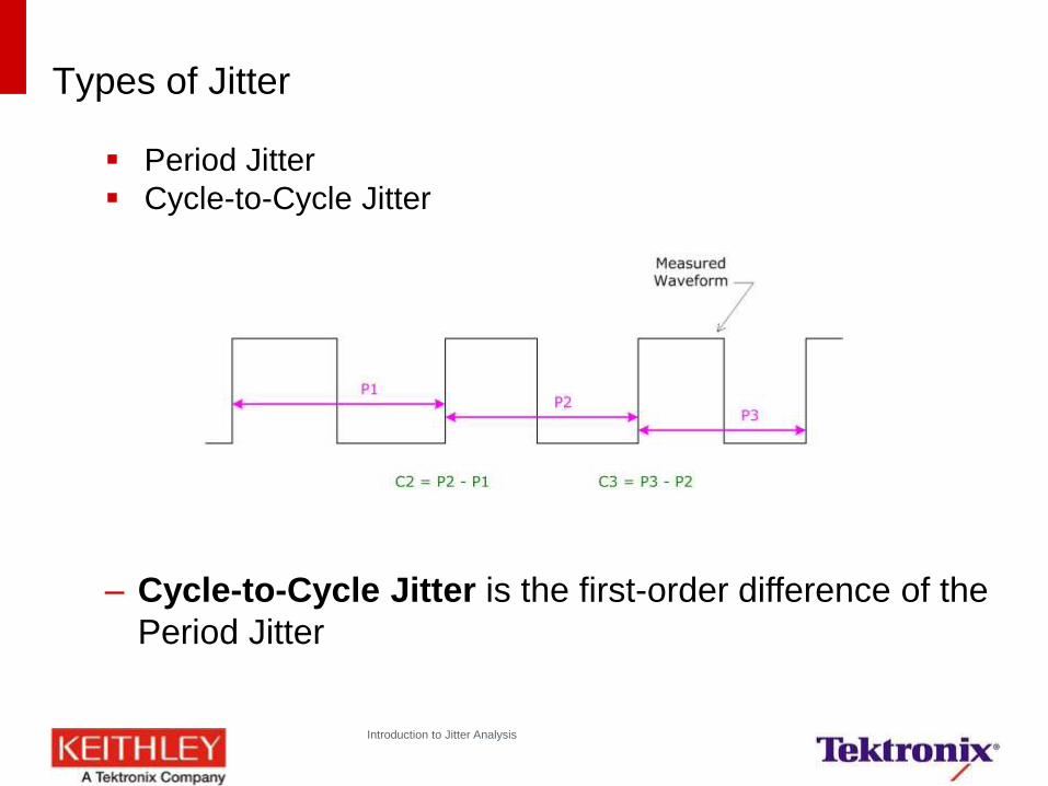
Types of Jitter
Introduction to Jitter Analysis
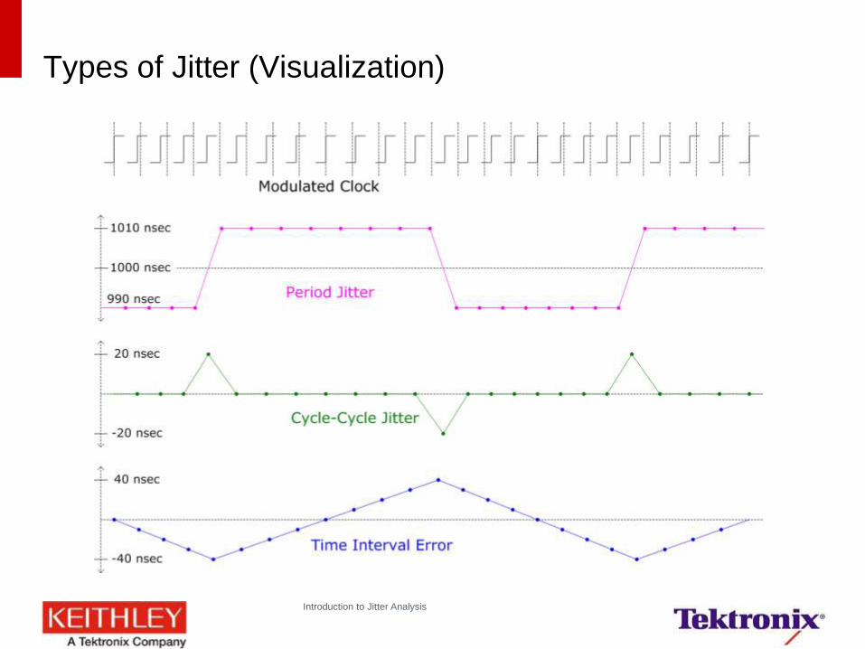
– Cycle-to-Cycle Jitter is the first-order difference of the
Period Jitter
Period Jitter
Cycle-to-Cycle Jitter

Types of Jitter (Visualization)
Introduction to Jitter Analysis
Types of Jitter
Introduction to Jitter Analysis
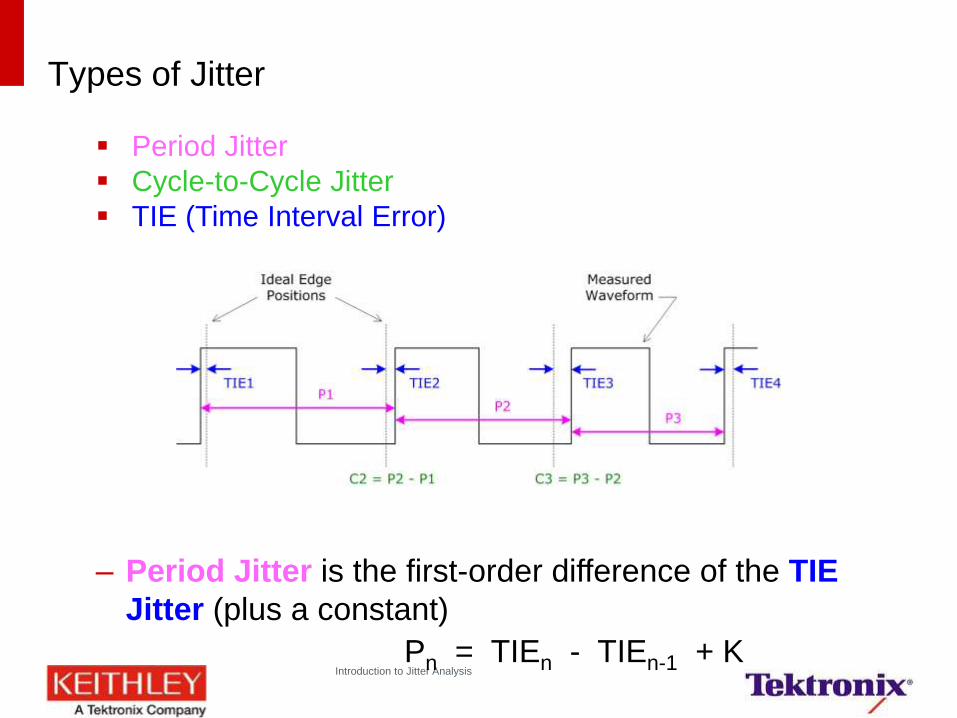
– Period Jitter is the first-order difference of the TIE
Jitter (plus a constant)
Pn = TIEn - TIEn-1 + K
Period Jitter
Cycle-to-Cycle Jitter
TIE (Time Interval Error)
Types of Jitter (Visualization)
Introduction to Jitter Analysis
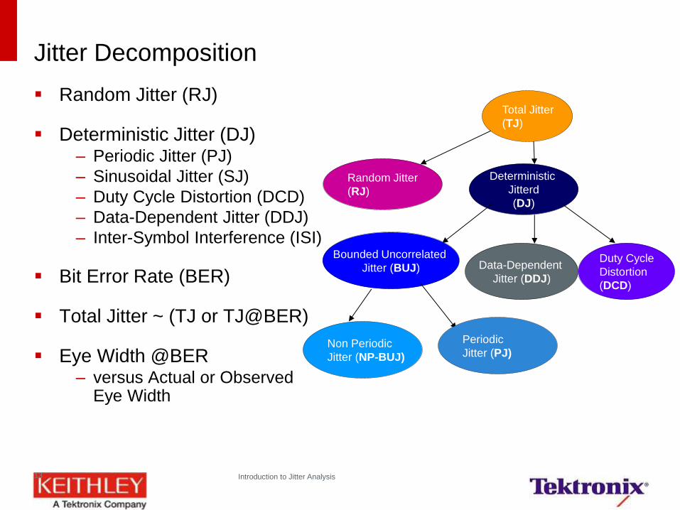
Jitter Decomposition
Random Jitter (RJ)
Deterministic Jitter (DJ) – Periodic Jitter (PJ)
– Sinusoidal Jitter (SJ)
– Duty Cycle Distortion (DCD)
– Data-Dependent Jitter (DDJ)
– Inter-Symbol Interference (ISI)
Bit Error Rate (BER)
Total Jitter ~ (TJ or TJ@BER)
Eye Width @BER – versus Actual or Observed
Eye Width
Introduction to Jitter Analysis 13
Deterministic
Jitterd
(DJ)
Random Jitter
(RJ)
Duty Cycle
Distortion
(DCD)
Data-Dependent
Jitter (DDJ)
Bounded Uncorrelated
Jitter (BUJ)
Periodic
Jitter (PJ) Non Periodic
Jitter (NP-BUJ)
Total Jitter
(TJ)
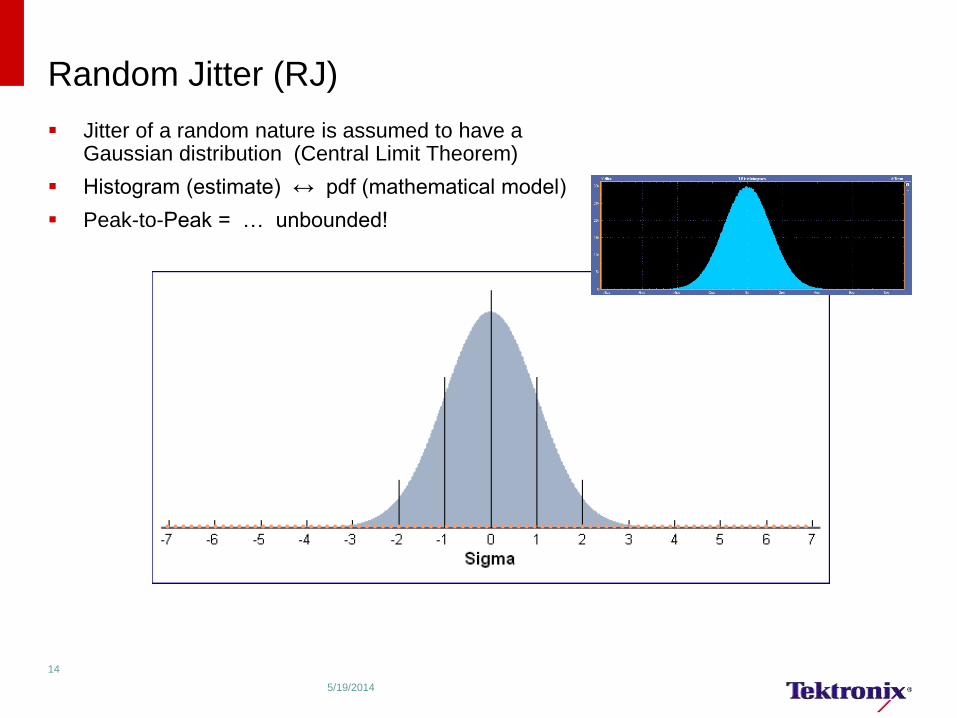
Random Jitter (RJ)
Jitter of a random nature is assumed to have a Gaussian distribution (Central Limit Theorem)
Histogram (estimate) ↔ pdf (mathematical model)
Peak-to-Peak = … unbounded!
5/19/2014
14

Deterministic Jitter (DJ)
Deterministic jitter has a bounded
distribution: the observed peak-to-peak
value will not grow over time
Histogram = pdf (close enough)
5/19/2014
15
Peak-to-Peak
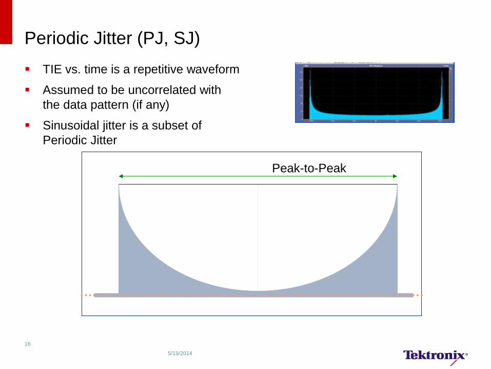
Periodic Jitter (PJ, SJ)
TIE vs. time is a repetitive waveform
Assumed to be uncorrelated with
the data pattern (if any)
Sinusoidal jitter is a subset of
Periodic Jitter
5/19/2014
16
Peak-to-Peak
Duty Cycle Distortion (DCD)
DCD is the difference between the mean TIE for rising
edges and the mean TIE for falling edges
Causes
– Asymmetrical rise-time vs. fall-time
– Non-optimal choice of decision threshold
For a clock signal, the pdf consists of two impulses
17
0.0v
-0.1v
Data-Dependent Jitter
DDJ or PDJ – used interchangeably
ISI – usually considered to be the physical effect that causes DDJ
Characterizes how the jitter on each transition is correlated with specific patterns of prior bits
– Due to the step response of the system
– Due to transmission line effects (e.g. reflections)
18
No ISI
24” ISI
40” ISI
Bounded Uncorrelated Jitter
Interconnect and board layout technology is
advancing and the greatest area of focus is in
reducing the insertion loss and Signal-to-
Crosstalk ratio.
The implications of complex channel interaction
can be observed and identified by examining the
type and amount of Bounded Uncorrelated Jitter
or BUJ.
There is a strong Cause–and-Effect relationship
between Crosstalk and BUJ which often gets
classified as Random if special steps are not
observed.
– Results in inflated TJ
– TJ = DJ = RJ*14 @ BER 10-12
BUJ vs. Legacy Jitter Decomposition Results
TJ@BER1, Math1 10.105ps
RJ1, Math1 506.04fs
PJ1, Math1 3.6968ps
DJ1, Math1 3.6968ps
NPJ1, Math1 881.89fs
TIE2, Math1 55.789fs
Rise Slew Rate1, Math1 9.2627V/ns
TJ@BER1, Math1 9.9087ps
RJ1, Math1 556.41fs
PJ1, Math1 2.6685ps
DJ1, Math1 2.6685ps
NPJ1, Math1 592.92fs
TIE2, Math1 89.108fs
Rise Slew Rate1, Math1 9.2542V/ns
TJ@BER1, Math1 10.315ps
RJ1, Math1 680.95fs
PJ1, Math1 1.7365ps
DJ1, Math1 1.7365ps
TIE2, Math1 44.029fs
Rise Slew Rate1, Math1 9.3228V/ns
TJ@BER1, Math1 11.159ps
RJ1, Math1 694.31fs
PJ1, Math1 2.8264ps
DJ1, Math1 2.8264ps
TIE2, Math1 -25.694fs
Rise Slew Rate1, Math1 9.2843V/ns
Legacy Decomposition New BUJ Decomposition
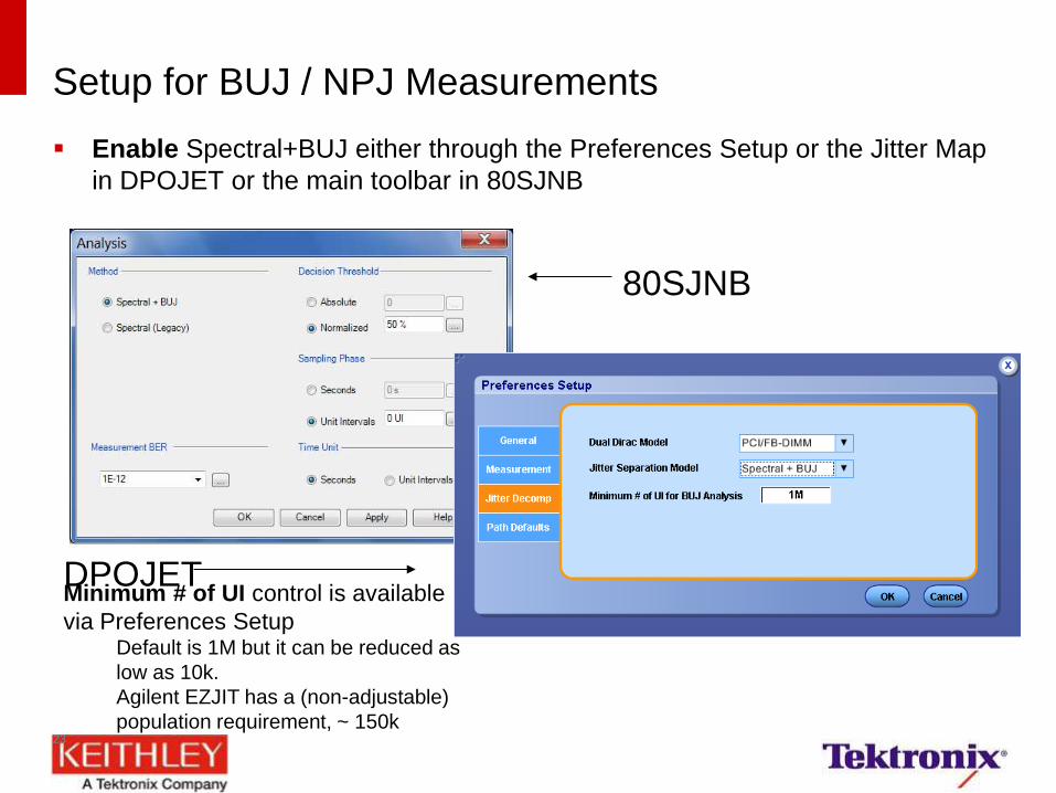
Setup for BUJ / NPJ Measurements
Enable Spectral+BUJ either through the Preferences Setup or the Jitter Map
in DPOJET or the main toolbar in 80SJNB
23
80SJNB
DPOJET Minimum # of UI control is available
via Preferences Setup Default is 1M but it can be reduced as
low as 10k.
Agilent EZJIT has a (non-adjustable)
population requirement, ~ 150k
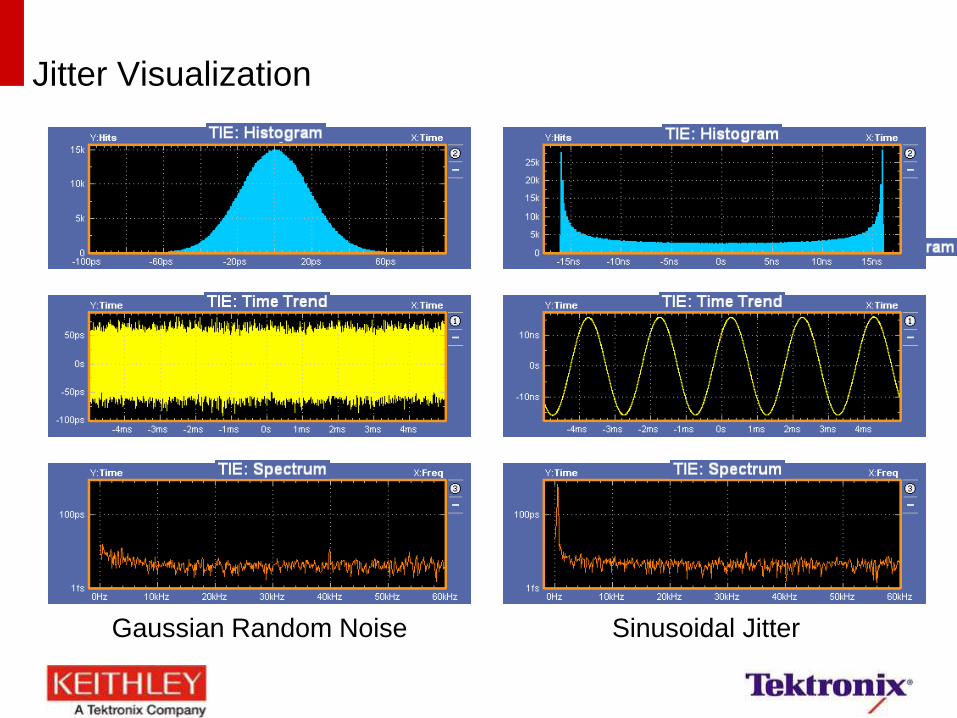
Jitter Visualization
Gaussian Random Noise Sinusoidal Jitter
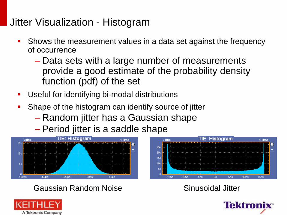
Jitter Visualization - Histogram
Gaussian Random Noise Sinusoidal Jitter
Shows the measurement values in a data set against the frequency of occurrence
– Data sets with a large number of measurements provide a good estimate of the probability density function (pdf) of the set
Useful for identifying bi-modal distributions
Shape of the histogram can identify source of jitter
– Random jitter has a Gaussian shape
– Period jitter is a saddle shape
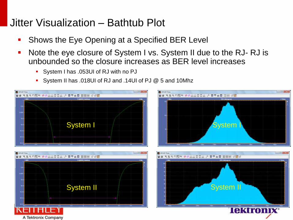
Jitter Visualization – Bathtub Plot
Shows the Eye Opening at a Specified BER Level
Note the eye closure of System I vs. System II due to the RJ- RJ is unbounded so the closure increases as BER level increases
System I has .053UI of RJ with no PJ
System II has .018UI of RJ and .14UI of PJ @ 5 and 10Mhz
System I System I
System II System II

5/19/2014 27
Jitter Visualization – Time Trend
Histogram does not have any context of time
Time Trend can reveal repeating patterns that may indicate modulation on the signal
For example 5 cycle of SSC @ 30khz as shown below
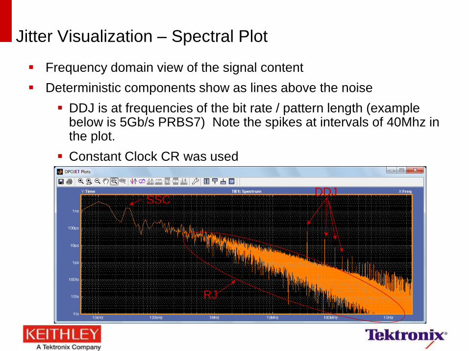
Jitter Visualization – Spectral Plot
Frequency domain view of the signal content
Deterministic components show as lines above the noise
DDJ is at frequencies of the bit rate / pattern length (example below is 5Gb/s PRBS7) Note the spikes at intervals of 40Mhz in the plot.
Constant Clock CR was used
DDJ
SSC
RJ
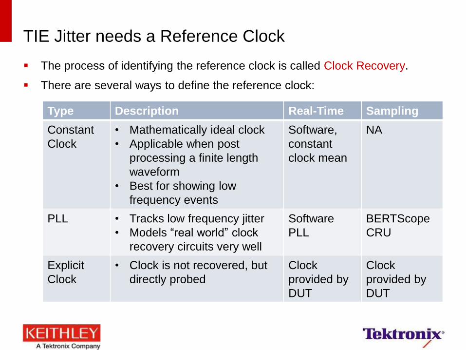
TIE Jitter needs a Reference Clock
The process of identifying the reference clock is called Clock Recovery.
There are several ways to define the reference clock:
Type Description Real-Time Sampling
Constant
Clock
• Mathematically ideal clock
• Applicable when post
processing a finite length
waveform
• Best for showing low
frequency events
Software,
constant
clock mean
NA
PLL • Tracks low frequency jitter
• Models “real world” clock
recovery circuits very well
Software
PLL
BERTScope
CRU
Explicit
Clock
• Clock is not recovered, but
directly probed
Clock
provided by
DUT
Clock
provided by
DUT
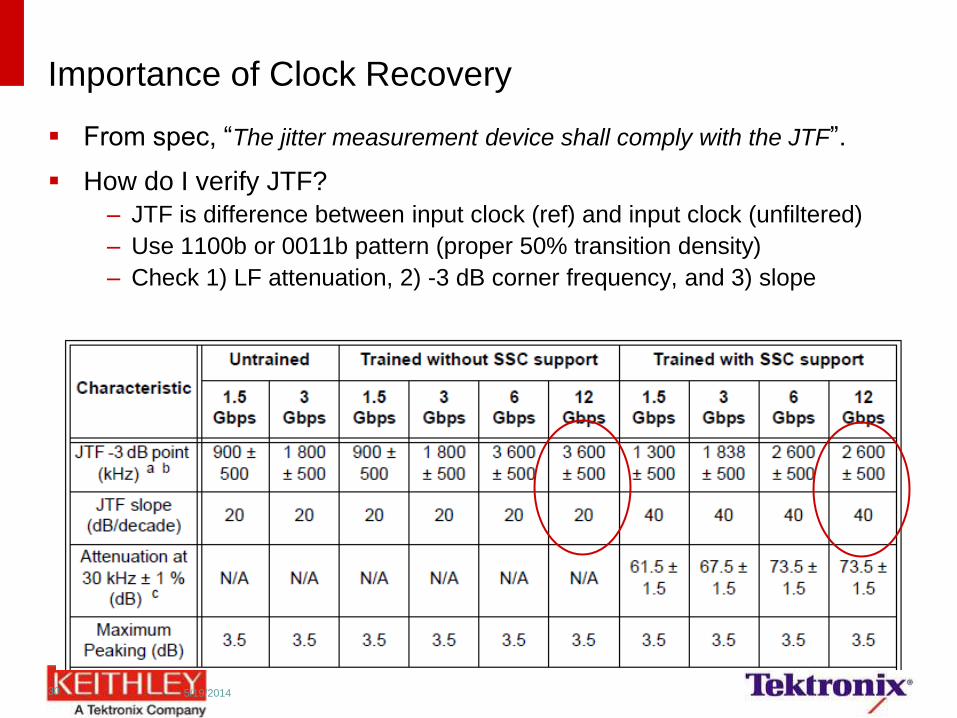
Importance of Clock Recovery
From spec, “The jitter measurement device shall comply with the JTF”.
How do I verify JTF?
– JTF is difference between input clock (ref) and input clock (unfiltered)
– Use 1100b or 0011b pattern (proper 50% transition density)
– Check 1) LF attenuation, 2) -3 dB corner frequency, and 3) slope
5/19/2014 30
JTF vs PLL Loop Bandwidth
Configuring the correct PLL settings is key to
correct measurements
Most standards have a reference/defined CR setup – For example, USB 3.0 uses a Type II with JTF of 4.9Mhz
Type I PLL – Type I PLL has 20dB of roll off per decade
– JTF and PLL Loop Bandwidth are Equal
Type 2 PLL – Type II PLL has 40dB of roll off per decade
– JTF and PLL Loop Bandwidth are not Equal
– For example, USB 3.0 uses a Type 2 PLL with a JTF of
4.9Mhz. The corresponding loop bandwidth is 10.126 Mhz
– Setting the Loop Bandwidth as opposed to JTF will lead to
incorrect jitter measurement results
31
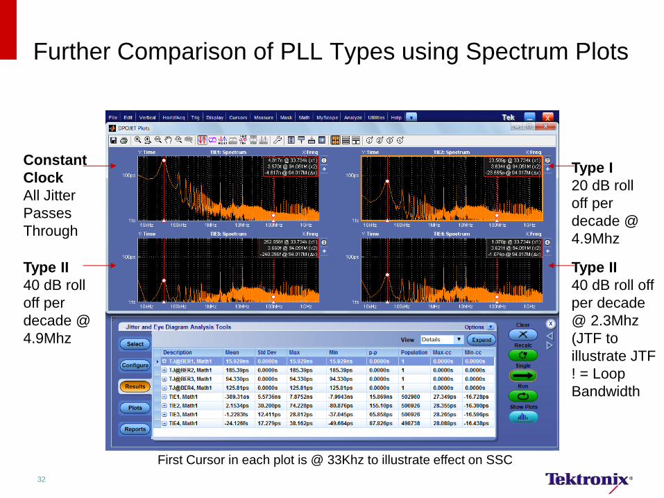
Further Comparison of PLL Types using Spectrum Plots
32
Constant
Clock
All Jitter
Passes
Through
Type I
20 dB roll
off per
decade @
4.9Mhz
Type II
40 dB roll
off per
decade @
4.9Mhz
Type II
40 dB roll off
per decade
@ 2.3Mhz
(JTF to
illustrate JTF
! = Loop
Bandwidth
First Cursor in each plot is @ 33Khz to illustrate effect on SSC
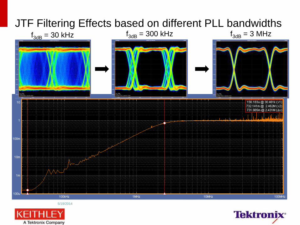
JTF Filtering Effects based on different PLL bandwidths
5/19/2014
f3dB = 30 kHz f3dB = 300 kHz f3dB = 3 MHz
HDMI – Introducing new HDMI 2.0
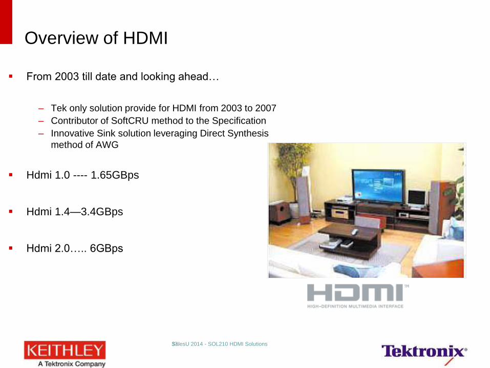
Overview of HDMI
From 2003 till date and looking ahead…
– Tek only solution provide for HDMI from 2003 to 2007
– Contributor of SoftCRU method to the Specification
– Innovative Sink solution leveraging Direct Synthesis
method of AWG
Hdmi 1.0 ---- 1.65GBps
Hdmi 1.4—3.4GBps
Hdmi 2.0….. 6GBps
37 SalesU 2014 - SOL210 HDMI Solutions
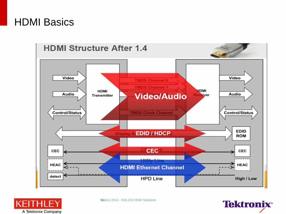
HDMI Basics
38 SalesU 2014 - SOL210 HDMI Solutions
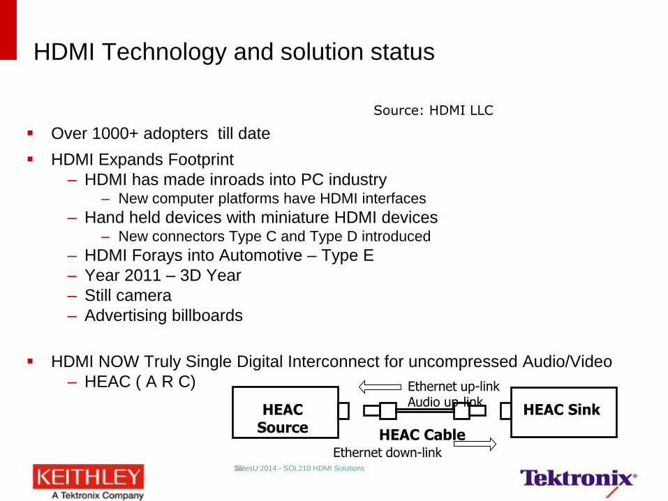
HDMI Technology and solution status
Over 1000+ adopters till date
HDMI Expands Footprint
– HDMI has made inroads into PC industry – New computer platforms have HDMI interfaces
– Hand held devices with miniature HDMI devices – New connectors Type C and Type D introduced
– HDMI Forays into Automotive – Type E
– Year 2011 – 3D Year
– Still camera
– Advertising billboards
HDMI NOW Truly Single Digital Interconnect for uncompressed Audio/Video
– HEAC ( A R C)
39
Source: HDMI LLC
Ethernet up-link Audio up-link
HEAC Source
HEAC Cable Ethernet down-link
HEAC Sink
SalesU 2014 - SOL210 HDMI Solutions
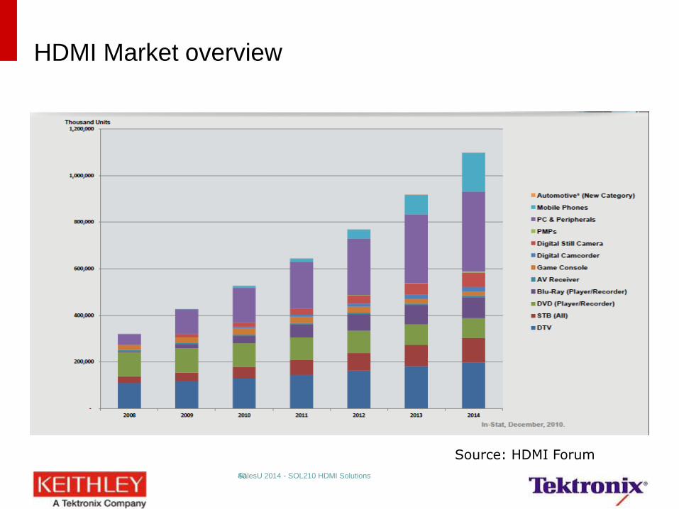
HDMI Market overview
40
Source: HDMI Forum
SalesU 2014 - SOL210 HDMI Solutions
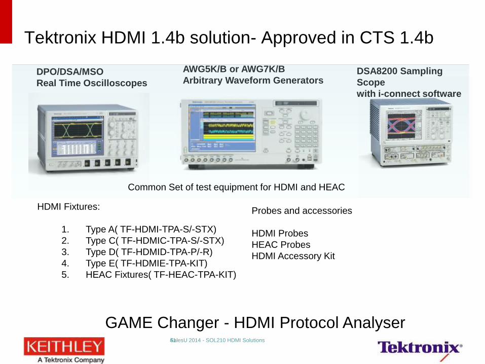
Tektronix HDMI 1.4b solution- Approved in CTS 1.4b
41
DPO/DSA/MSO
Real Time Oscilloscopes
AWG5K/B or AWG7K/B
Arbitrary Waveform Generators DSA8200 Sampling
Scope
with i-connect software
Common Set of test equipment for HDMI and HEAC
HDMI Fixtures:
1. Type A( TF-HDMI-TPA-S/-STX)
2. Type C( TF-HDMIC-TPA-S/-STX)
3. Type D( TF-HDMID-TPA-P/-R)
4. Type E( TF-HDMIE-TPA-KIT)
5. HEAC Fixtures( TF-HEAC-TPA-KIT)
Probes and accessories
HDMI Probes
HEAC Probes
HDMI Accessory Kit
GAME Changer - HDMI Protocol Analyser SalesU 2014 - SOL210 HDMI Solutions
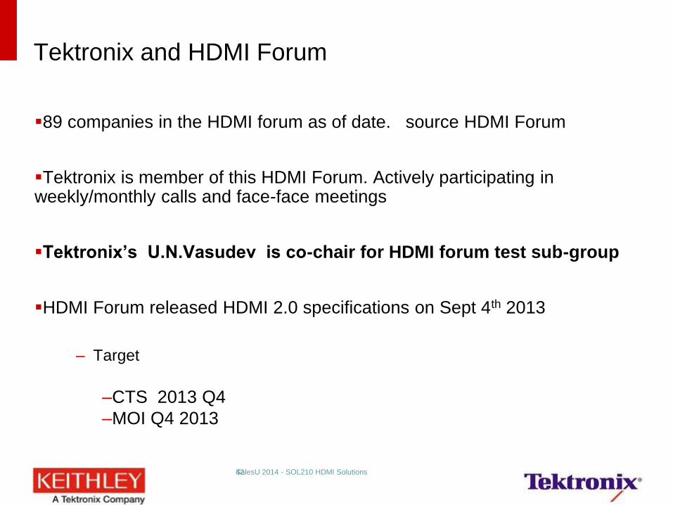
Tektronix and HDMI Forum
89 companies in the HDMI forum as of date. source HDMI Forum
Tektronix is member of this HDMI Forum. Actively participating in weekly/monthly calls and face-face meetings
Tektronix’s U.N.Vasudev is co-chair for HDMI forum test sub-group
HDMI Forum released HDMI 2.0 specifications on Sept 4th 2013
– Target
–CTS 2013 Q4
–MOI Q4 2013
42 SalesU 2014 - SOL210 HDMI Solutions
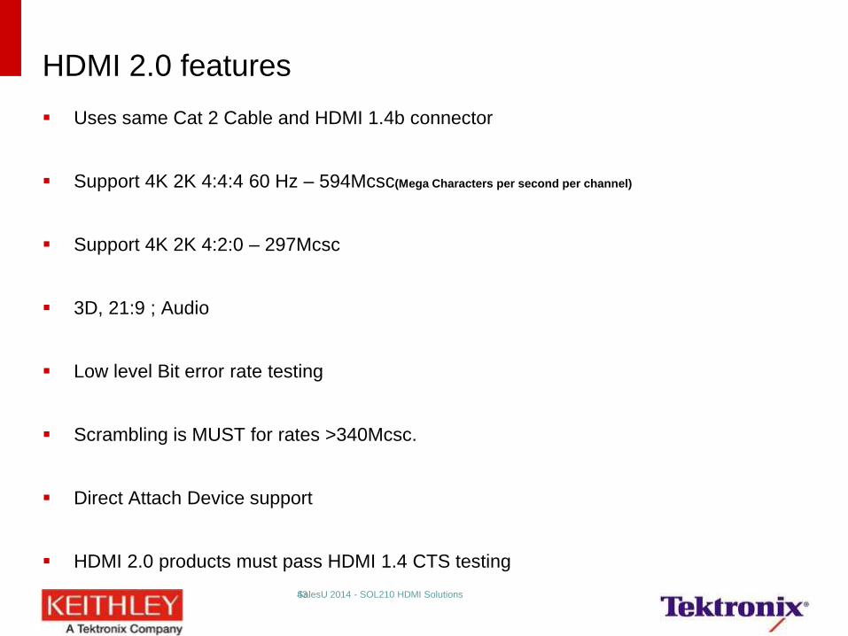
HDMI 2.0 features
Uses same Cat 2 Cable and HDMI 1.4b connector
Support 4K 2K 4:4:4 60 Hz – 594Mcsc(Mega Characters per second per channel)
Support 4K 2K 4:2:0 – 297Mcsc
3D, 21:9 ; Audio
Low level Bit error rate testing
Scrambling is MUST for rates >340Mcsc.
Direct Attach Device support
HDMI 2.0 products must pass HDMI 1.4 CTS testing
43 SalesU 2014 - SOL210 HDMI Solutions
44
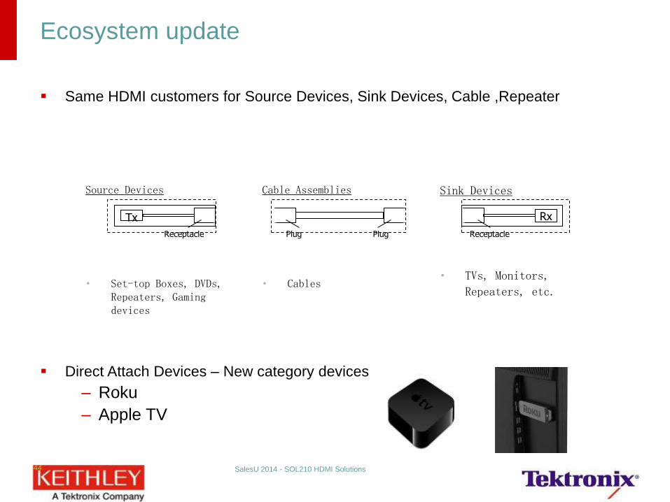
Same HDMI customers for Source Devices, Sink Devices, Cable ,Repeater
Direct Attach Devices – New category devices
– Roku
– Apple TV
Ecosystem update
Plug Plug Receptacle
Tx
Receptacle
Rx
Sink Devices
• TVs, Monitors,
Repeaters, etc.
Source Devices
• Set-top Boxes, DVDs, Repeaters, Gaming devices
Cable Assemblies
• Cables
SalesU 2014 - SOL210 HDMI Solutions
HDMI 2.0 Solutions Portfolio
( Source setup, Sink Setup,
Protocol Decode, Probes)
45 SalesU 2014 - SOL210 HDMI Solutions
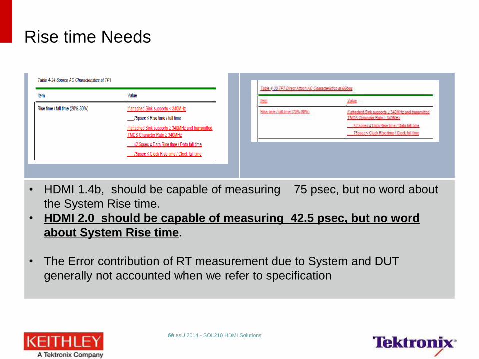
Rise time Needs
• HDMI 1.4b, should be capable of measuring 75 psec, but no word about
the System Rise time.
• HDMI 2.0 should be capable of measuring 42.5 psec, but no word
about System Rise time.
• The Error contribution of RT measurement due to System and DUT
generally not accounted when we refer to specification
46 SalesU 2014 - SOL210 HDMI Solutions
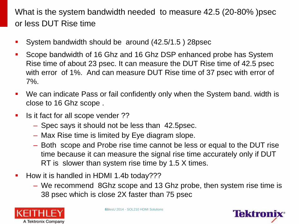
What is the system bandwidth needed to measure 42.5 (20-80% )psec
or less DUT Rise time
System bandwidth should be around (42.5/1.5 ) 28psec
Scope bandwidth of 16 Ghz and 16 Ghz DSP enhanced probe has System
Rise time of about 23 psec. It can measure the DUT Rise time of 42.5 psec
with error of 1%. And can measure DUT Rise time of 37 psec with error of
7%.
We can indicate Pass or fail confidently only when the System band. width is
close to 16 Ghz scope .
Is it fact for all scope vender ??
– Spec says it should not be less than 42.5psec.
– Max Rise time is limited by Eye diagram slope.
– Both scope and Probe rise time cannot be less or equal to the DUT rise
time because it can measure the signal rise time accurately only if DUT
RT is slower than system rise time by 1.5 X times.
How it is handled in HDMI 1.4b today???
– We recommend 8Ghz scope and 13 Ghz probe, then system rise time is
38 psec which is close 2X faster than 75 psec
47 SalesU 2014 - SOL210 HDMI Solutions
Conclusion
16GHz BW scope will give 1% error and hence is recommended for
HDMI 2.0 testing.
HDMI 2.0 RT/FT (20%-80%) data signals is 42.5ps
Note: We also support 12.5GHz BW scope for HDMI 2.0 but will have a
10% error in RT/FT measurements
48 SalesU 2014 - SOL210 HDMI Solutions
Source Testing 1.4b Vs 2.0
Eye Diagram and Clock Jitter test is now performed at TP2
Rest of the tests is same as HDMI 1.4b
1.4b CTS test is a pre-requsite for HDMI 2.0
Min 8GHz scope to 16GHz scope
New Fixtures
Same Probes
HDM and HDM-DS Software
49 SalesU 2014 - SOL210 HDMI Solutions
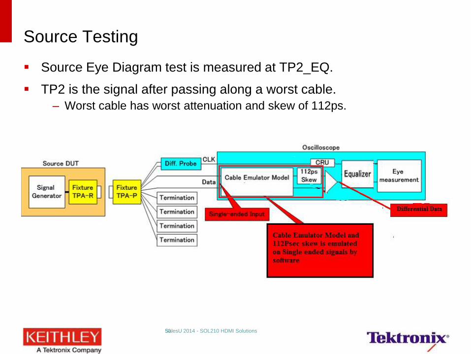
Source Testing
Source Eye Diagram test is measured at TP2_EQ.
TP2 is the signal after passing along a worst cable.
– Worst cable has worst attenuation and skew of 112ps.
50 SalesU 2014 - SOL210 HDMI Solutions
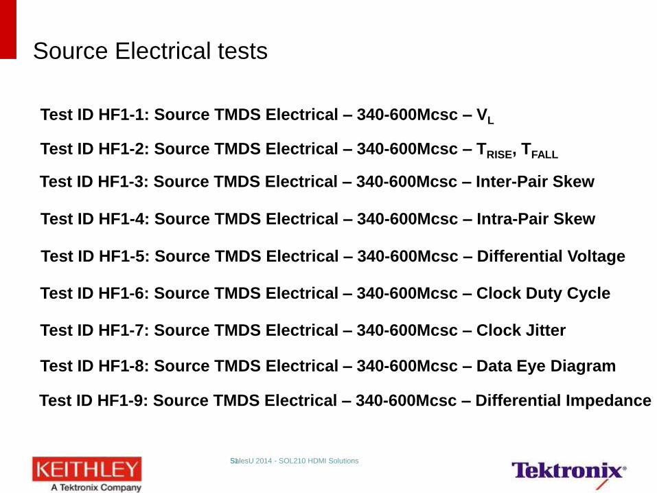
Source Electrical tests
51
Test ID HF1-1: Source TMDS Electrical – 340-600Mcsc – VL
Test ID HF1-2: Source TMDS Electrical – 340-600Mcsc – TRISE, TFALL
Test ID HF1-3: Source TMDS Electrical – 340-600Mcsc – Inter-Pair Skew
Test ID HF1-4: Source TMDS Electrical – 340-600Mcsc – Intra-Pair Skew
Test ID HF1-5: Source TMDS Electrical – 340-600Mcsc – Differential Voltage
Test ID HF1-6: Source TMDS Electrical – 340-600Mcsc – Clock Duty Cycle
Test ID HF1-7: Source TMDS Electrical – 340-600Mcsc – Clock Jitter
Test ID HF1-8: Source TMDS Electrical – 340-600Mcsc – Data Eye Diagram
Test ID HF1-9: Source TMDS Electrical – 340-600Mcsc – Differential Impedance
SalesU 2014 - SOL210 HDMI Solutions

Source Eye Diagram Test
52
SMA Pair Cable
HDMI Source
Clk +
Clk -
Tektronix Oscilloscope
DPO/DSA/MSO70000 Series ≧ 16GHz
Include Reference Cable Emulator (s4p) and Reference Cable Equalizer
HDMI Plug Fixture
with EDID Emulator
Data + Data -
Diff Clk
SE Data
TF-HDMI-TPA-T
SalesU 2014 - SOL210 HDMI Solutions
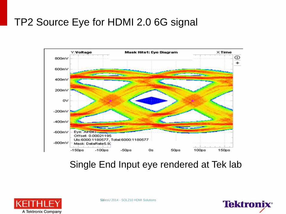
TP2 Source Eye for HDMI 2.0 6G signal
53
Single End Input eye rendered at Tek lab
SalesU 2014 - SOL210 HDMI Solutions
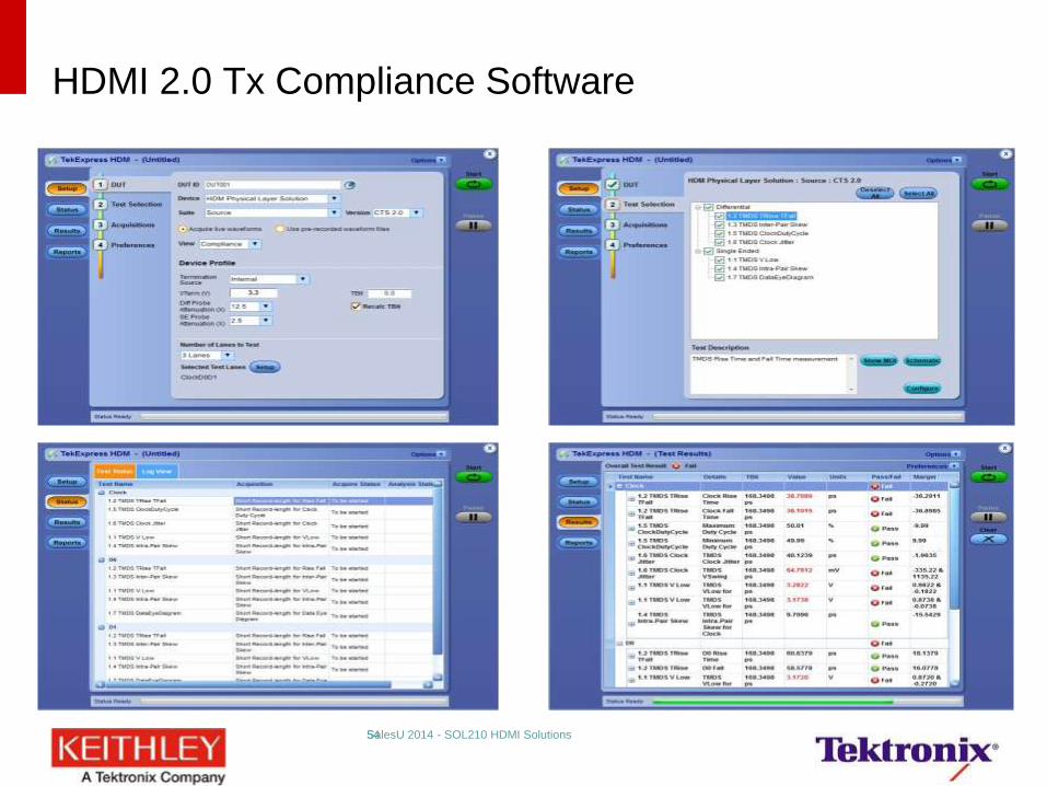
HDMI 2.0 Tx Compliance Software
54 SalesU 2014 - SOL210 HDMI Solutions
HDMI 2.0 Sink testing Equipment needs
16GHz BW scope will give 1% error and hence is recommended for HDMI 2.0 Sink
testing for Jitter Verification/Calibration/Controller.
P7313SMA probes > 3
Option HDM and HDM-DS
HDMI 2.0 Fixture set
2# AWG7122C with Opt 01,02 or 06, 08 for HDMI 2.0 Compliance only setup. OR
2# AWG70002A with Opt 01,03 and 225 for HDMI 2.0 Compliance and Margin Test setup.(Margin
test feature will be available later and is part of roadmap)
Note- We shall also support a 12.5GHz BW scope which would result in appx. 10% inaccuracy in RT/FT
results .
SalesU 2014 - SOL210 HDMI Solutions
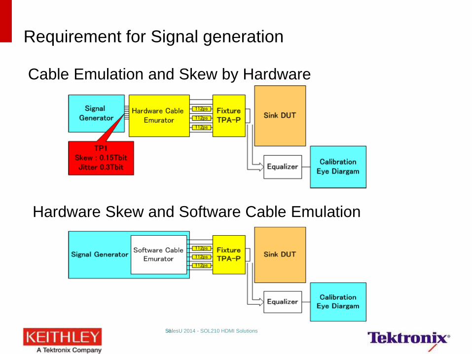
Requirement for Signal generation
56
Hardware Skew and Software Cable Emulation
Cable Emulation and Skew by Hardware
SalesU 2014 - SOL210 HDMI Solutions
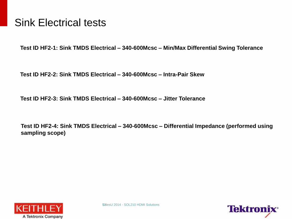
Sink Electrical tests
57
Test ID HF2-1: Sink TMDS Electrical – 340-600Mcsc – Min/Max Differential Swing Tolerance
Test ID HF2-2: Sink TMDS Electrical – 340-600Mcsc – Intra-Pair Skew
Test ID HF2-3: Sink TMDS Electrical – 340-600Mcsc – Jitter Tolerance
Test ID HF2-4: Sink TMDS Electrical – 340-600Mcsc – Differential Impedance (performed using
sampling scope)
SalesU 2014 - SOL210 HDMI Solutions

HDMI 2.0 Rx solution positioning statement
Tektronix will support HDMI 2.0 Sink Electrical and protocol tests
using either 2# AWG7122C (w/ Opt 01,02/06,08) OR 2# AWG70002A
(W/ Opt 01,03 ,225)
Solution Positioning:
– Compliance solution for HDMI 2.0 Rx
– 2# AWG7122C with opt 01, 02/06 and 08
– 1# AFG3102/C
Customers can use common test setup for HDMI 1.4b and HDMI 2.0 giving
value for their investment in Tektronix HDMI 1.4b Rx solution.
– Compliance and Margin solution for HDMI 2.0 Rx – 2# AWG70002A with Opt 01,03 and 225.
– 1# AFG3102/C
Customers can use common test setup for HDMI 1.4b and HDMI 2.0 giving
value for their investment in Tektronix HDMI 1.4b Rx solution
SalesU 2014 - SOL210 HDMI Solutions
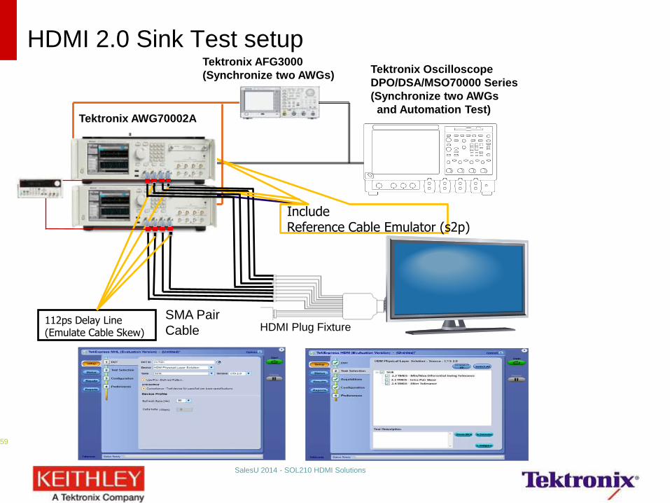
HDMI 2.0 Sink Test setup
HDMI Sink
59
HDMI Plug Fixture
Tektronix AFG3000
(Synchronize two AWGs)
Tektronix AWG70002A
Tektronix Oscilloscope
DPO/DSA/MSO70000 Series
(Synchronize two AWGs
and Automation Test)
SMA Pair
Cable 112ps Delay Line (Emulate Cable Skew)
Include Reference Cable Emulator (s2p)
SalesU 2014 - SOL210 HDMI Solutions
Sink Testing 1.4b Vs 2.0
Jitter Tolerance test needs +ve and –ve lanes tested with 112ps delay line
Rest of the tests is similar to HDMI 1.4b tests
1.4b CTS test is a pre-requsite for HDMI 2.0
Need AWG 70002A for HDMI 2.0 Compliance and Margin needs while
AWG7122C is suitable for HDMI 2.0 Compliance testing only..
Min 8GHz scope to 16GHz scope
Fixtures and Probes
HDM and HDM-DS Software
60 SalesU 2014 - SOL210 HDMI Solutions
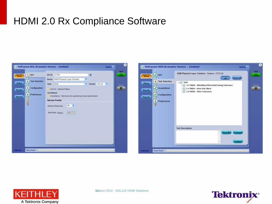
HDMI 2.0 Rx Compliance Software
61 SalesU 2014 - SOL210 HDMI Solutions
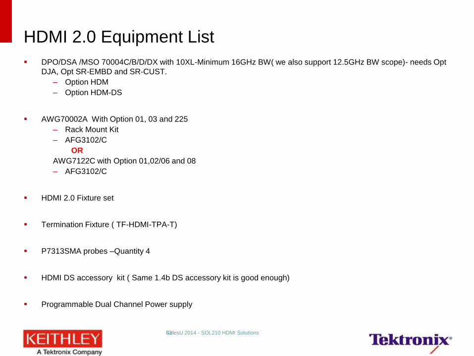
HDMI 2.0 Equipment List
DPO/DSA /MSO 70004C/B/D/DX with 10XL-Minimum 16GHz BW( we also support 12.5GHz BW scope)- needs Opt
DJA, Opt SR-EMBD and SR-CUST.
– Option HDM
– Option HDM-DS
AWG70002A With Option 01, 03 and 225
– Rack Mount Kit
– AFG3102/C
OR
AWG7122C with Option 01,02/06 and 08
– AFG3102/C
HDMI 2.0 Fixture set
Termination Fixture ( TF-HDMI-TPA-T)
P7313SMA probes –Quantity 4
HDMI DS accessory kit ( Same 1.4b DS accessory kit is good enough)
Programmable Dual Channel Power supply
62 SalesU 2014 - SOL210 HDMI Solutions
SATA/SAS – Storage standard
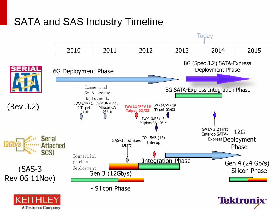
SATA and SAS Industry Timeline
Today
2010 2011
6G Deployment Phase
– Commercial Gen3 product deployment.
– Commercial product
deployment. Gen 4 (24 Gb/s) - Silicon Phase
2012
IW#9/PF#14 Taipei 11/16
SAS-3 first Spec Draft
IW#10/PF#15 Milpitas CA
05/16
IW#11/PF#16 Taipei 03/23
2013 2014
IW#13/PF#18 Milpitas CA 10/14
IW#14/PF#19 Taipei 03/03
8G SATA-Express Integration Phase
SATA 3.2 First Interop SATA-
Express
8G (Spec 3.2) SATA-Express Deployment Phase
IOL SAS (12)
Interop
Integration Phase
12G Deployment
Phase
(Rev 3.2)
Gen 3 (12Gb/s)
- Silicon Phase
(SAS-3 Rev 06 11Nov)
2015
Embedded Applications SATA BGA
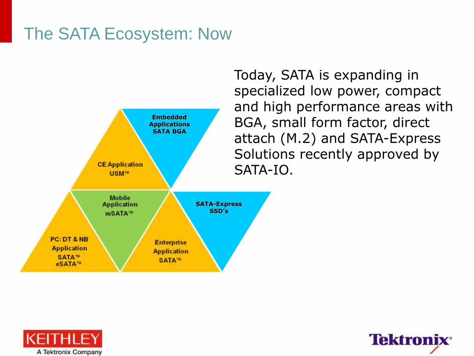
Today, SATA is expanding in specialized low power, compact and high performance areas with BGA, small form factor, direct attach (M.2) and SATA-Express Solutions recently approved by SATA-IO.
The SATA Ecosystem: Now
SATA-Express SSD’s
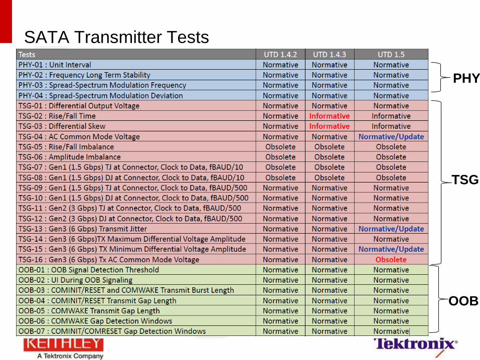
SATA Transmitter Tests
PHY
TSG
OOB
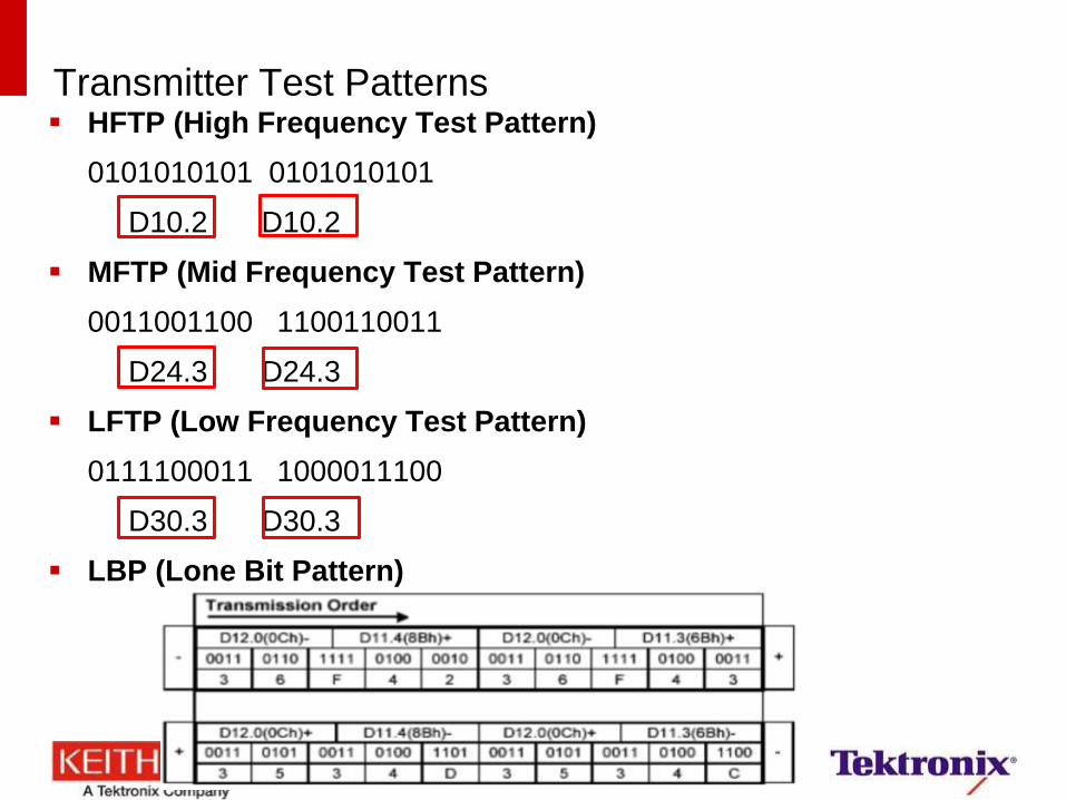
Transmitter Test Patterns HFTP (High Frequency Test Pattern)
0101010101 0101010101
D10.2 D10.2
MFTP (Mid Frequency Test Pattern)
0011001100 1100110011
D24.3 D24.3
LFTP (Low Frequency Test Pattern)
0111100011 1000011100
D30.3 D30.3
LBP (Lone Bit Pattern)
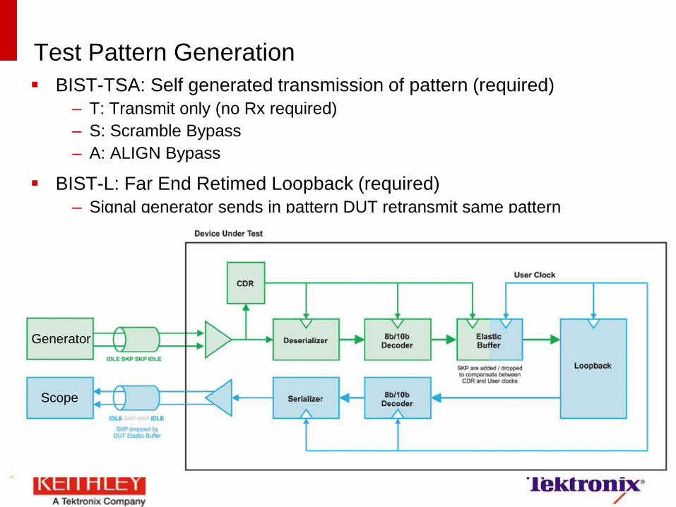
Test Pattern Generation
BIST-TSA: Self generated transmission of pattern (required)
– T: Transmit only (no Rx required)
– S: Scramble Bypass
– A: ALIGN Bypass
BIST-L: Far End Retimed Loopback (required)
– Signal generator sends in pattern DUT retransmit same pattern
Generator
Scope
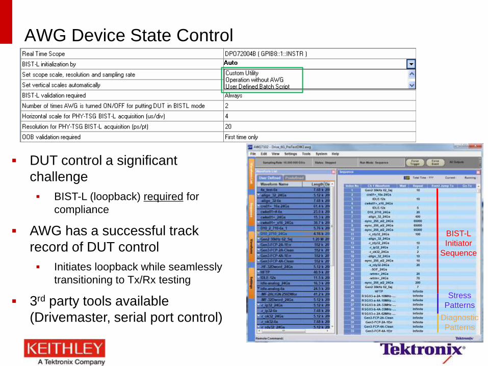
AWG Device State Control
DUT control a significant
challenge
BIST-L (loopback) required for
compliance
AWG has a successful track
record of DUT control
Initiates loopback while seamlessly
transitioning to Tx/Rx testing
3rd party tools available
(Drivemaster, serial port control)
BIST-L
Initiator
Sequence
Stress
Patterns
Diagnostic
Patterns
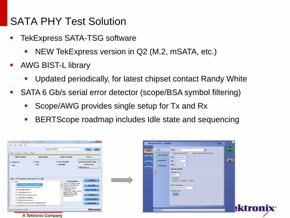
SATA PHY Test Solution
TekExpress SATA-TSG software
NEW TekExpress version in Q2 (M.2, mSATA, etc.)
AWG BIST-L library
Updated periodically, for latest chipset contact Randy White
SATA 6 Gb/s serial error detector (scope/BSA symbol filtering)
Scope/AWG provides single setup for Tx and Rx
BERTScope roadmap includes Idle state and sequencing
Introduction to SAS
74
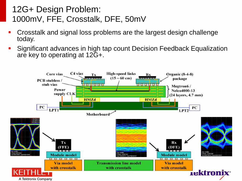
12G+ Design Problem: 1000mV, FFE, Crosstalk, DFE, 50mV
Crosstalk and signal loss problems are the largest design challenge today.
Significant advances in high tap count Decision Feedback Equalization are key to operating at 12G+.
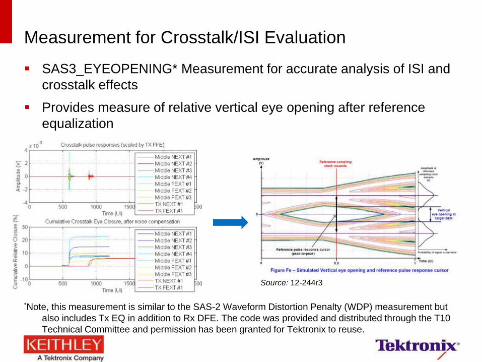
Measurement for Crosstalk/ISI Evaluation
SAS3_EYEOPENING* Measurement for accurate analysis of ISI and
crosstalk effects
Provides measure of relative vertical eye opening after reference
equalization
*Note, this measurement is similar to the SAS-2 Waveform Distortion Penalty (WDP) measurement but
also includes Tx EQ in addition to Rx DFE. The code was provided and distributed through the T10
Technical Committee and permission has been granted for Tektronix to reuse.
Source: 12-244r3
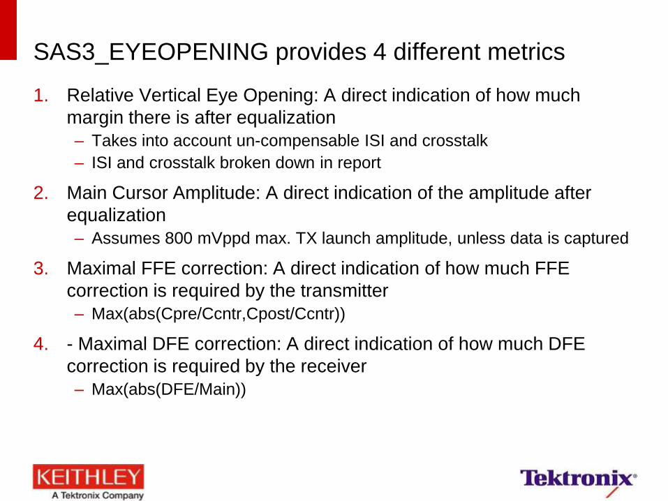
SAS3_EYEOPENING provides 4 different metrics
1. Relative Vertical Eye Opening: A direct indication of how much
margin there is after equalization
– Takes into account un-compensable ISI and crosstalk
– ISI and crosstalk broken down in report
2. Main Cursor Amplitude: A direct indication of the amplitude after
equalization
– Assumes 800 mVppd max. TX launch amplitude, unless data is captured
3. Maximal FFE correction: A direct indication of how much FFE
correction is required by the transmitter
– Max(abs(Cpre/Ccntr,Cpost/Ccntr))
4. - Maximal DFE correction: A direct indication of how much DFE
correction is required by the receiver
– Max(abs(DFE/Main))
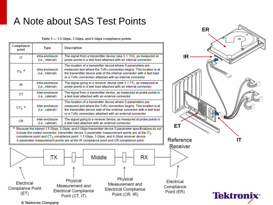
A Note about SAS Test Points
IT
ER
ET
IR
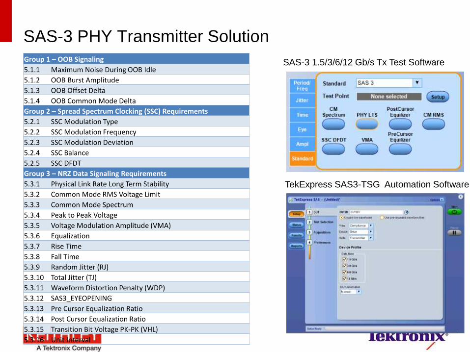
SAS-3 PHY Transmitter Solution
SAS-3 1.5/3/6/12 Gb/s Tx Test Software
TekExpress SAS3-TSG Automation Software
Group 1 – OOB Signaling
5.1.1 Maximum Noise During OOB Idle
5.1.2 OOB Burst Amplitude
5.1.3 OOB Offset Delta
5.1.4 OOB Common Mode Delta
Group 2 – Spread Spectrum Clocking (SSC) Requirements
5.2.1 SSC Modulation Type
5.2.2 SSC Modulation Frequency
5.2.3 SSC Modulation Deviation
5.2.4 SSC Balance
5.2.5 SSC DFDT
Group 3 – NRZ Data Signaling Requirements
5.3.1 Physical Link Rate Long Term Stability
5.3.2 Common Mode RMS Voltage Limit
5.3.3 Common Mode Spectrum
5.3.4 Peak to Peak Voltage
5.3.5 Voltage Modulation Amplitude (VMA)
5.3.6 Equalization
5.3.7 Rise Time
5.3.8 Fall Time
5.3.9 Random Jitter (RJ)
5.3.10 Total Jitter (TJ)
5.3.11 Waveform Distortion Penalty (WDP)
5.3.12 SAS3_EYEOPENING
5.3.13 Pre Cursor Equalization Ratio
5.3.14 Post Cursor Equalization Ratio
5.3.15 Transition Bit Voltage PK-PK (VHL)
5.3.16 Unit Interval
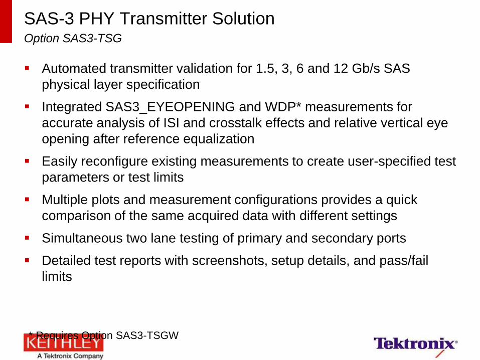
SAS-3 PHY Transmitter Solution Option SAS3-TSG
Automated transmitter validation for 1.5, 3, 6 and 12 Gb/s SAS
physical layer specification
Integrated SAS3_EYEOPENING and WDP* measurements for
accurate analysis of ISI and crosstalk effects and relative vertical eye
opening after reference equalization
Easily reconfigure existing measurements to create user-specified test
parameters or test limits
Multiple plots and measurement configurations provides a quick
comparison of the same acquired data with different settings
Simultaneous two lane testing of primary and secondary ports
Detailed test reports with screenshots, setup details, and pass/fail
limits
* Requires Option SAS3-TSGW
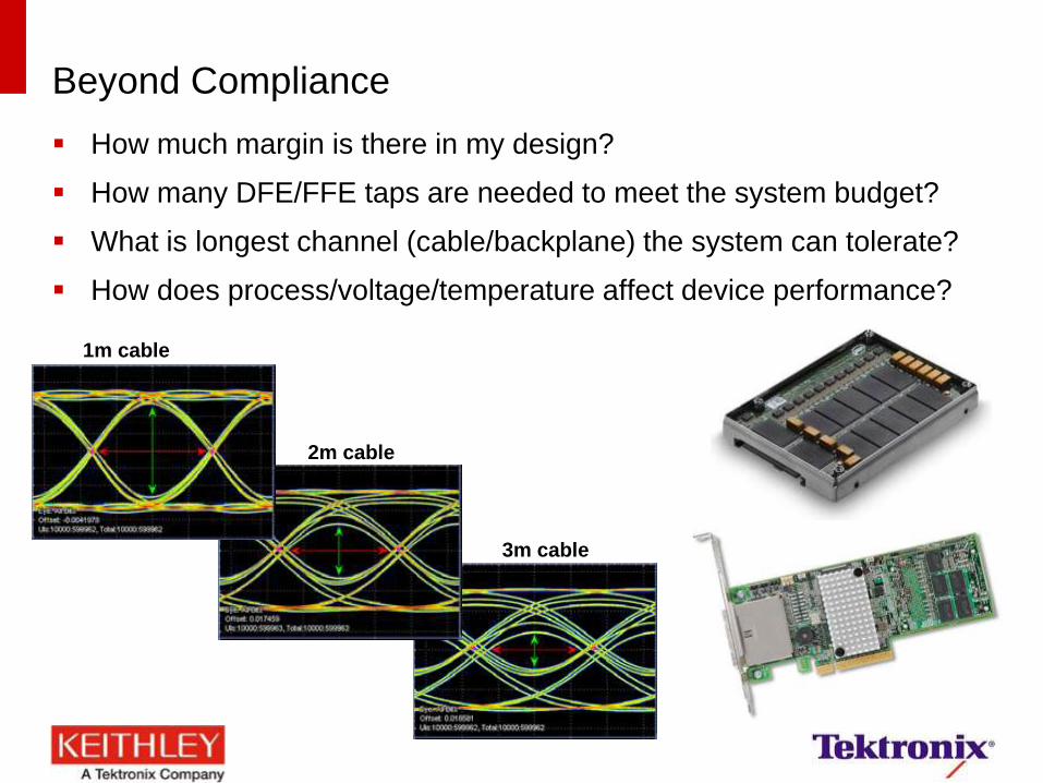
Beyond Compliance
How much margin is there in my design?
How many DFE/FFE taps are needed to meet the system budget?
What is longest channel (cable/backplane) the system can tolerate?
How does process/voltage/temperature affect device performance?
1m cable
2m cable
3m cable
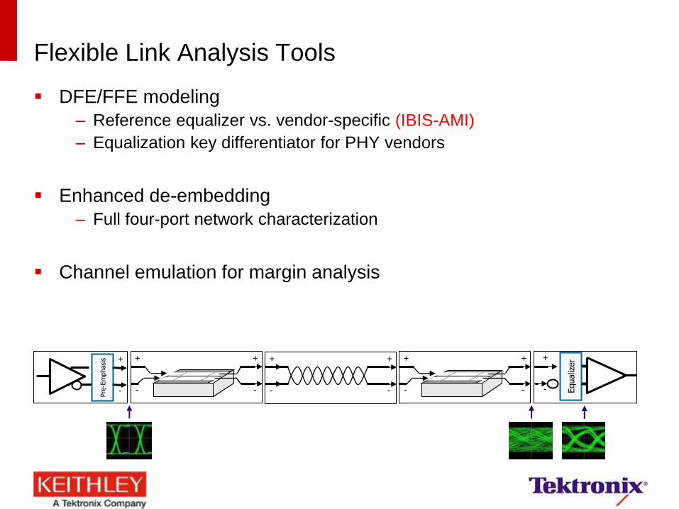
Flexible Link Analysis Tools
DFE/FFE modeling
– Reference equalizer vs. vendor-specific (IBIS-AMI)
– Equalization key differentiator for PHY vendors
Enhanced de-embedding
– Full four-port network characterization
Channel emulation for margin analysis
+
-
+
-
+
-
+
-
+
-
+
-
+
-
+
- Equaliz
er
Pre
-Em
phasi
s
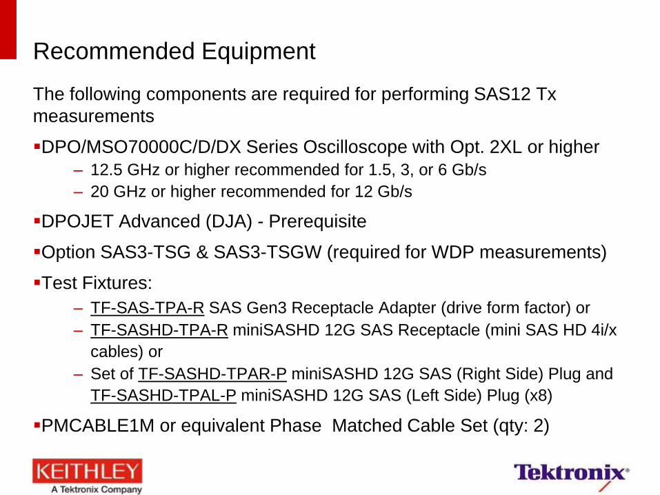
Recommended Equipment
The following components are required for performing SAS12 Tx
measurements
DPO/MSO70000C/D/DX Series Oscilloscope with Opt. 2XL or higher
– 12.5 GHz or higher recommended for 1.5, 3, or 6 Gb/s
– 20 GHz or higher recommended for 12 Gb/s
DPOJET Advanced (DJA) - Prerequisite
Option SAS3-TSG & SAS3-TSGW (required for WDP measurements)
Test Fixtures:
– TF-SAS-TPA-R SAS Gen3 Receptacle Adapter (drive form factor) or
– TF-SASHD-TPA-R miniSASHD 12G SAS Receptacle (mini SAS HD 4i/x
cables) or
– Set of TF-SASHD-TPAR-P miniSASHD 12G SAS (Right Side) Plug and
TF-SASHD-TPAL-P miniSASHD 12G SAS (Left Side) Plug (x8)
PMCABLE1M or equivalent Phase Matched Cable Set (qty: 2)
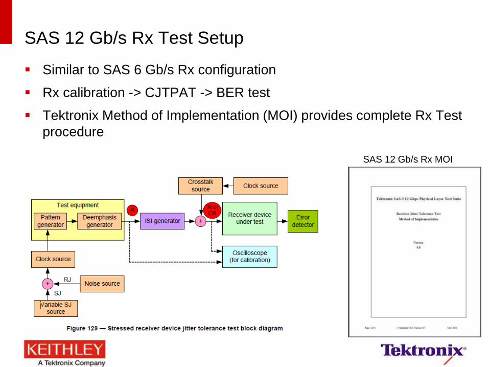
SAS 12 Gb/s Rx Test Setup
Similar to SAS 6 Gb/s Rx configuration
Rx calibration -> CJTPAT -> BER test
Tektronix Method of Implementation (MOI) provides complete Rx Test
procedure
SAS 12 Gb/s Rx MOI
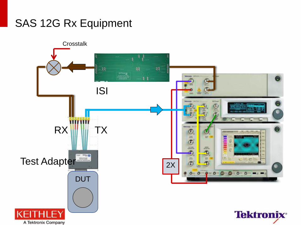
SAS 12G Rx Equipment
DUT
Crosstalk
2X Test Adapter
ISI
RX TX
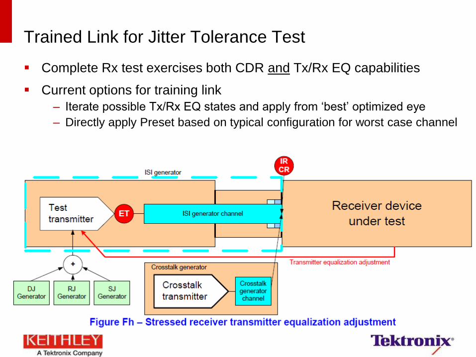
Trained Link for Jitter Tolerance Test
Complete Rx test exercises both CDR and Tx/Rx EQ capabilities
Current options for training link
– Iterate possible Tx/Rx EQ states and apply from ‘best’ optimized eye
– Directly apply Preset based on typical configuration for worst case channel
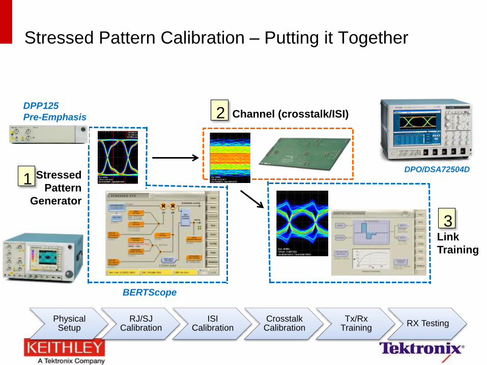
Stressed Pattern Calibration – Putting it Together
Stressed
Pattern
Generator
Link
Training
BERTScope
DPP125
Pre-Emphasis
Channel (crosstalk/ISI)
1
2
3
DPO/DSA72504D
Physical Setup
RJ/SJ Calibration
ISI Calibration
Crosstalk Calibration
Tx/Rx Training
RX Testing
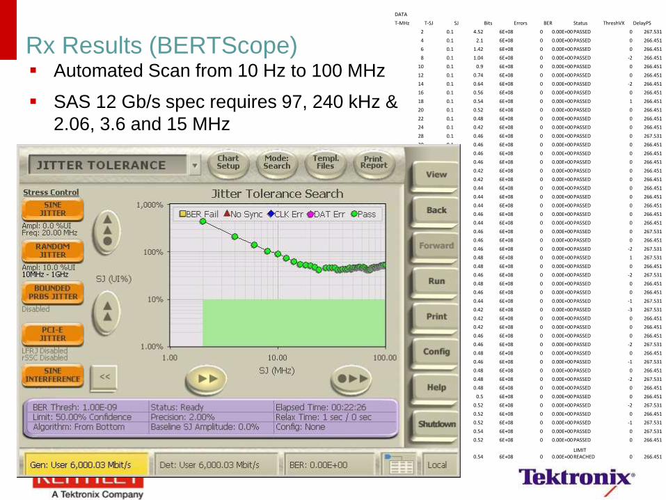
Rx Results (BERTScope)
DATA
T-MHz T-SJ SJ Bits Errors BER Status ThreshVX DelayPS
2 0.1 4.52 6E+08 0 0.00E+00 PASSED 0 267.531
4 0.1 2.1 6E+08 0 0.00E+00 PASSED 0 266.451
6 0.1 1.42 6E+08 0 0.00E+00 PASSED 0 266.451
8 0.1 1.04 6E+08 0 0.00E+00 PASSED -2 266.451
10 0.1 0.9 6E+08 0 0.00E+00 PASSED 0 266.451
12 0.1 0.74 6E+08 0 0.00E+00 PASSED 0 266.451
14 0.1 0.64 6E+08 0 0.00E+00 PASSED -2 266.451
16 0.1 0.56 6E+08 0 0.00E+00 PASSED 0 266.451
18 0.1 0.54 6E+08 0 0.00E+00 PASSED 1 266.451
20 0.1 0.52 6E+08 0 0.00E+00 PASSED 0 266.451
22 0.1 0.48 6E+08 0 0.00E+00 PASSED 0 266.451
24 0.1 0.42 6E+08 0 0.00E+00 PASSED 0 266.451
28 0.1 0.46 6E+08 0 0.00E+00 PASSED 0 267.531
30 0.1 0.46 6E+08 0 0.00E+00 PASSED 0 266.451
32 0.1 0.46 6E+08 0 0.00E+00 PASSED 0 266.451
34 0.1 0.46 6E+08 0 0.00E+00 PASSED 0 266.451
36 0.1 0.42 6E+08 0 0.00E+00 PASSED 0 266.451
38 0.1 0.42 6E+08 0 0.00E+00 PASSED 0 266.451
40 0.1 0.44 6E+08 0 0.00E+00 PASSED 0 266.451
42 0.1 0.44 6E+08 0 0.00E+00 PASSED 0 266.451
44 0.1 0.44 6E+08 0 0.00E+00 PASSED 0 266.451
46 0.1 0.46 6E+08 0 0.00E+00 PASSED 0 266.451
48 0.1 0.44 6E+08 0 0.00E+00 PASSED 0 266.451
50 0.1 0.46 6E+08 0 0.00E+00 PASSED 0 267.531
52 0.1 0.46 6E+08 0 0.00E+00 PASSED 0 266.451
54 0.1 0.46 6E+08 0 0.00E+00 PASSED -2 267.531
56 0.1 0.48 6E+08 0 0.00E+00 PASSED 1 267.531
58 0.1 0.48 6E+08 0 0.00E+00 PASSED 0 266.451
60 0.1 0.46 6E+08 0 0.00E+00 PASSED -2 267.531
62 0.1 0.48 6E+08 0 0.00E+00 PASSED 0 266.451
64 0.1 0.46 6E+08 0 0.00E+00 PASSED 0 266.451
66 0.1 0.44 6E+08 0 0.00E+00 PASSED -1 267.531
68 0.1 0.42 6E+08 0 0.00E+00 PASSED -3 267.531
70 0.1 0.42 6E+08 0 0.00E+00 PASSED 0 266.451
72 0.1 0.42 6E+08 0 0.00E+00 PASSED 0 266.451
74 0.1 0.46 6E+08 0 0.00E+00 PASSED 0 266.451
76 0.1 0.46 6E+08 0 0.00E+00 PASSED -2 267.531
78 0.1 0.48 6E+08 0 0.00E+00 PASSED 0 266.451
80 0.1 0.46 6E+08 0 0.00E+00 PASSED -1 267.531
82 0.1 0.48 6E+08 0 0.00E+00 PASSED 0 266.451
84 0.1 0.48 6E+08 0 0.00E+00 PASSED -2 267.531
86 0.1 0.48 6E+08 0 0.00E+00 PASSED 0 266.451
88 0.1 0.5 6E+08 0 0.00E+00 PASSED 0 266.451
90 0.1 0.52 6E+08 0 0.00E+00 PASSED -2 267.531
92 0.1 0.52 6E+08 0 0.00E+00 PASSED 0 266.451
94 0.1 0.52 6E+08 0 0.00E+00 PASSED -1 267.531
96 0.1 0.54 6E+08 0 0.00E+00 PASSED 0 267.531
98 0.1 0.52 6E+08 0 0.00E+00 PASSED 0 266.451
100 0.1 0.54 6E+08 0 0.00E+00 LIMIT REACHED 0 266.451
Automated Scan from 10 Hz to 100 MHz
SAS 12 Gb/s spec requires 97, 240 kHz &
2.06, 3.6 and 15 MHz
DDR – DDR4 Time
89
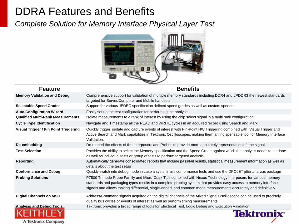
Feature Benefits Memory Validation and Debug Comprehensive support for validation of multiple memory standards including DDR4 and LPDDR3 the newest standards
targeted for Server/Computer and Mobile handsets.
Selectable Speed Grades Support for various JEDEC specification defined speed grades as well as custom speeds
Auto Configuration Wizard Easily set up the test configuration for performing the analysis.
Qualified Multi-Rank Measurements Isolate measurements to a rank of interest by using the chip select signal in a multi rank configuration
Cycle Type Identification Navigate and Timestamp all the READ and WRITE cycles in an acquired record using Search and Mark
Visual Trigger / Pin Point Triggering
Quickly trigger, isolate and capture events of interest with Pin-Point HW Triggering combined with Visual Trigger and
Active Search and Mark capabilities in Tektronix Oscilloscopes, making them an indispensable tool for Memory Interface
Validation.
De-embedding De-embed the effects of the Interposers and Probes to provide more accurately representation of the signal.
Test Selection Provides the ability to select the Memory specification and the Speed Grade against which the analysis needs to be done
as well as individual tests or group of tests to perform targeted analysis.
Reporting Automatically generate consolidated reports that include pass/fail results, statistical measurement information as well as
details about the test setup
Conformance and Debug Quickly switch into debug mode in case a system fails conformance tests and use the DPOJET jitter analysis package
Probing Solutions
P7500 Trimode Probe Family and Micro-Coax Tips combined with Nexus Technology Interposers for various memory
standards and packaging types results in a complete probing system that provides easy access to memory interface
signals and allows making differential, single-ended, and common mode measurements accurately and definitively
Digital Channels on MSO
Address/Command signals acquired on the digital channels of the Mixed Signal Oscilloscope can be used to precisely
qualify bus cycles or events of interest as well as perform timing measurements
Analysis and Debug Tools Tektronix provides a broad range of tools for Electrical Test, Logic Debug and Execution Validation.
DDRA Features and Benefits Complete Solution for Memory Interface Physical Layer Test
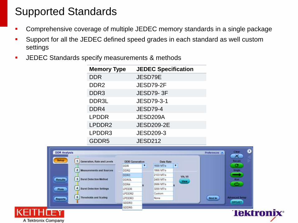
Supported Standards Comprehensive coverage of multiple JEDEC memory standards in a single package
Support for all the JEDEC defined speed grades in each standard as well custom
settings
JEDEC Standards specify measurements & methods
Memory Type JEDEC Specification
DDR JESD79E
DDR2 JESD79-2F
DDR3 JESD79- 3F
DDR3L JESD79-3-1
DDR4 JESD79-4
LPDDR JESD209A
LPDDR2 JESD209-2E
LPDDR3 JESD209-3
GDDR5 JESD212
www.tektronix.com/ddr
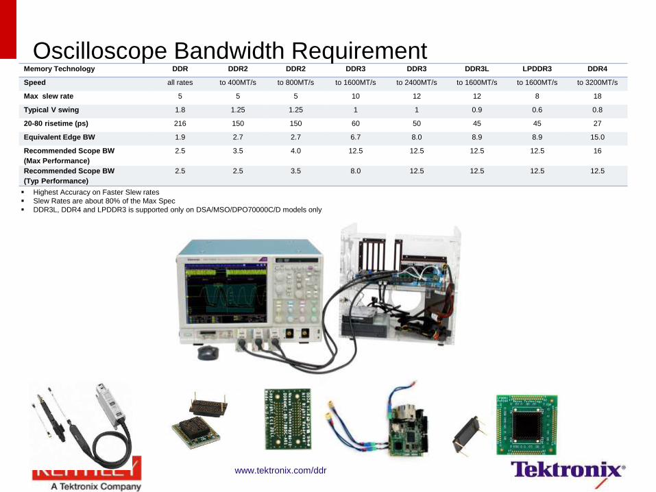
Memory Technology DDR DDR2 DDR2 DDR3 DDR3 DDR3L LPDDR3 DDR4
Speed all rates to 400MT/s to 800MT/s to 1600MT/s to 2400MT/s to 1600MT/s to 1600MT/s to 3200MT/s
Max slew rate 5 5 5 10 12 12 8 18
Typical V swing 1.8 1.25 1.25 1 1 0.9 0.6 0.8
20-80 risetime (ps) 216 150 150 60 50 45 45 27
Equivalent Edge BW 1.9 2.7 2.7 6.7 8.0 8.9 8.9 15.0
Recommended Scope BW
(Max Performance)
2.5 3.5 4.0 12.5 12.5 12.5 12.5 16
Recommended Scope BW
(Typ Performance)
2.5 2.5 3.5 8.0 12.5 12.5 12.5 12.5
Highest Accuracy on Faster Slew rates
Slew Rates are about 80% of the Max Spec
DDR3L, DDR4 and LPDDR3 is supported only on DSA/MSO/DPO70000C/D models only
Oscilloscope Bandwidth Requirement
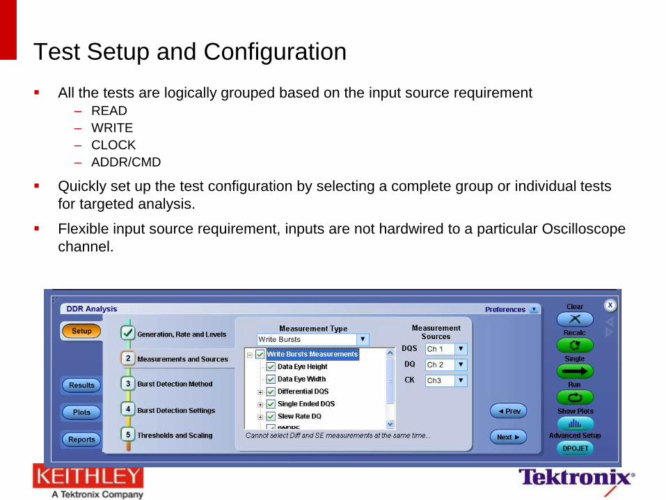
Test Setup and Configuration
All the tests are logically grouped based on the input source requirement
– READ
– WRITE
– CLOCK
– ADDR/CMD
Quickly set up the test configuration by selecting a complete group or individual tests
for targeted analysis.
Flexible input source requirement, inputs are not hardwired to a particular Oscilloscope
channel.

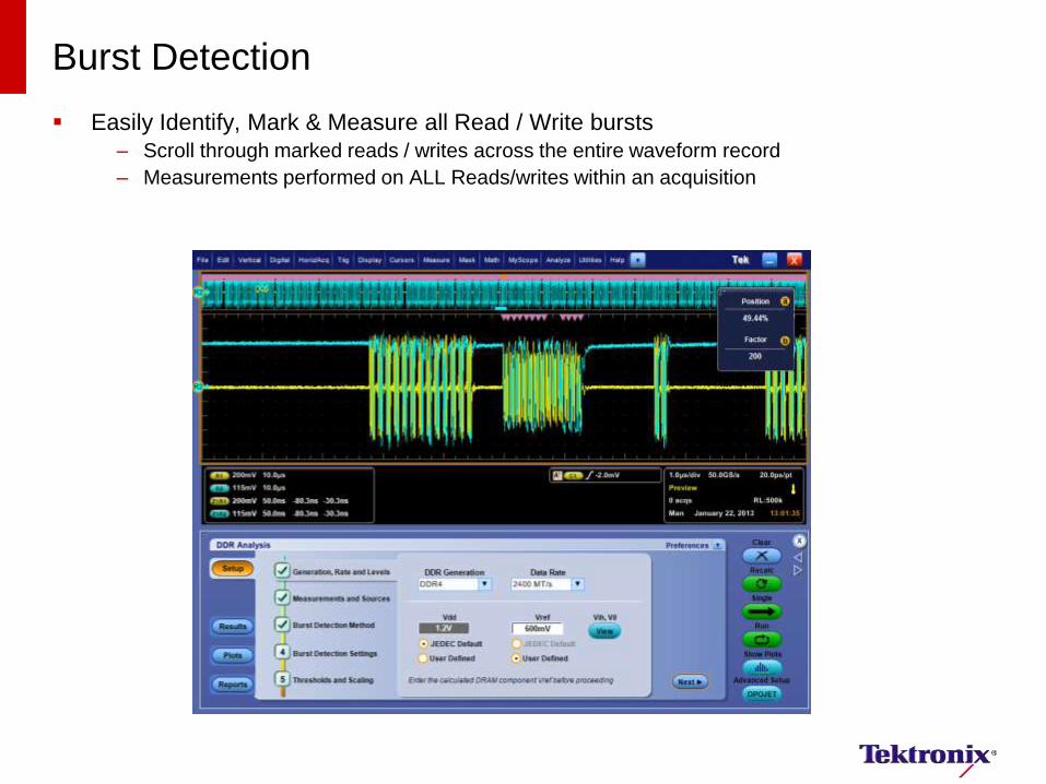
Burst Detection
Read / Write bursts are automatically detected for
analysis purposes
Several different techniques are used for Read/Write
Burst Separation – DQ/DQS phase alignment: DQ and DQS have different
phase relationship in Read and Write bursts
– CS, Latency + DQ/DQS Phase Alignment: CS is used
to quality the occurrence of a burst, followed by DQ/DS
phase relationship to distinguish between Read/Write
– Logic State + Burst latency: The command bus probed
using the digital channels on the MSO is used to
identify Read/Write commands on the command bus
are quality and distinguish Read and Write bursts
Options are provided to adjust the levels to improve
burst detection in systems with lower signal integrity
Burst Detection
Easily Identify, Mark & Measure all Read / Write bursts
– Scroll through marked reads / writes across the entire waveform record
– Measurements performed on ALL Reads/writes within an acquisition
96
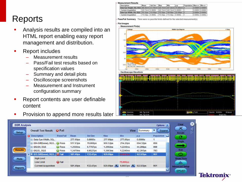
Reports Analysis results are compiled into an
HTML report enabling easy report
management and distribution.
Report includes – Measurement results
– Pass/Fail test results based on
specification values
– Summary and detail plots
– Oscilloscope screenshots
– Measurement and Instrument
configuration summary
Report contents are user definable
content
Provision to append more results later
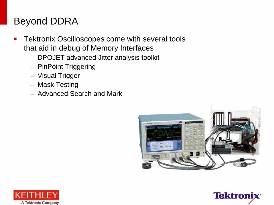
Beyond DDRA
Tektronix Oscilloscopes come with several tools
that aid in debug of Memory Interfaces
– DPOJET advanced Jitter analysis toolkit
– PinPoint Triggering
– Visual Trigger
– Mask Testing
– Advanced Search and Mark
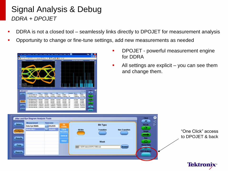
Signal Analysis & Debug DDRA + DPOJET
DDRA is not a closed tool – seamlessly links directly to DPOJET for measurement analysis
Opportunity to change or fine-tune settings, add new measurements as needed
“One Click” access
to DPOJET & back
DPOJET - powerful measurement engine
for DDRA
All settings are explicit – you can see them
and change them.
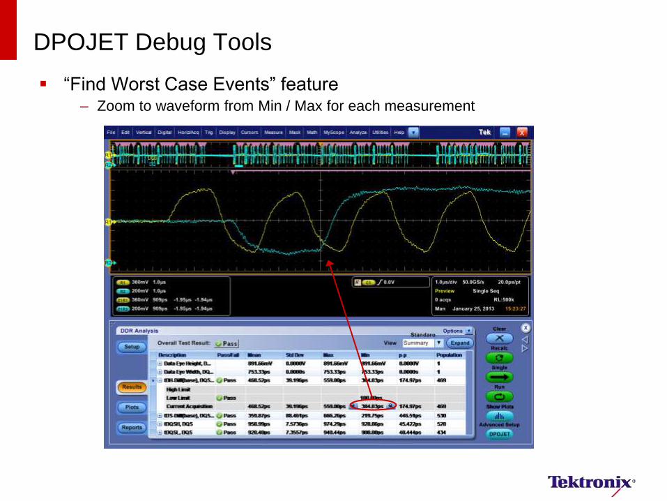
DPOJET Debug Tools
“Find Worst Case Events” feature – Zoom to waveform from Min / Max for each measurement
Pinpoint Triggering
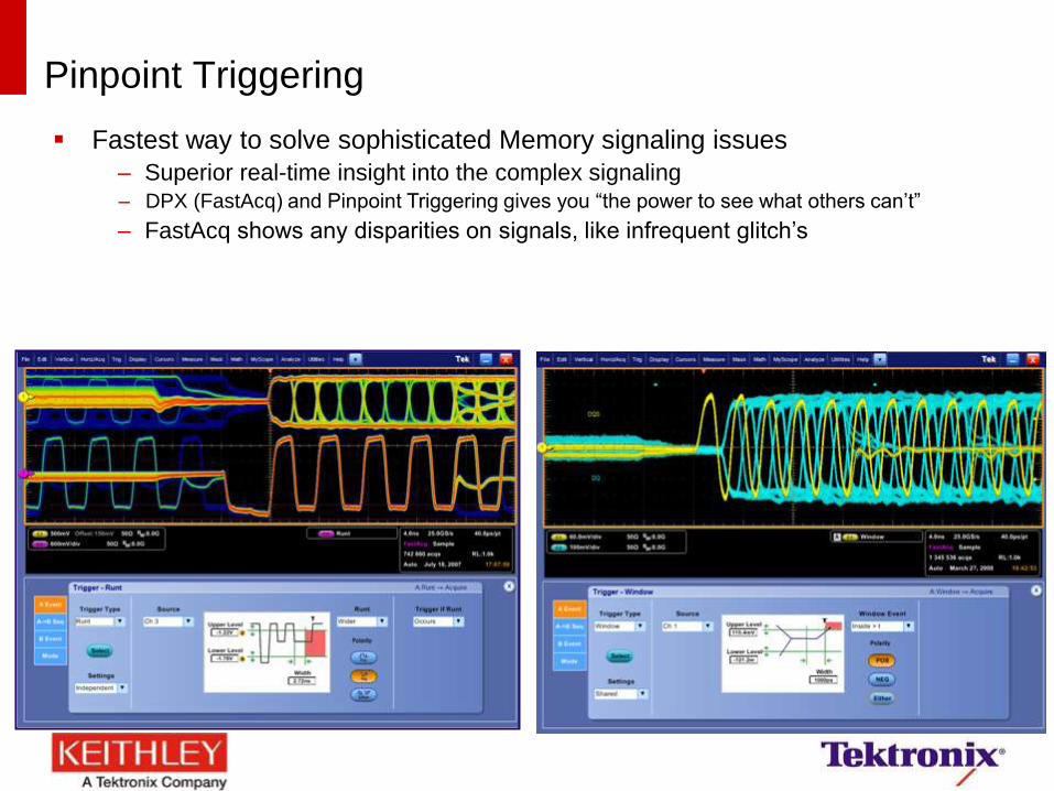
Fastest way to solve sophisticated Memory signaling issues
– Superior real-time insight into the complex signaling
– DPX (FastAcq) and Pinpoint Triggering gives you “the power to see what others can’t”
– FastAcq shows any disparities on signals, like infrequent glitch’s
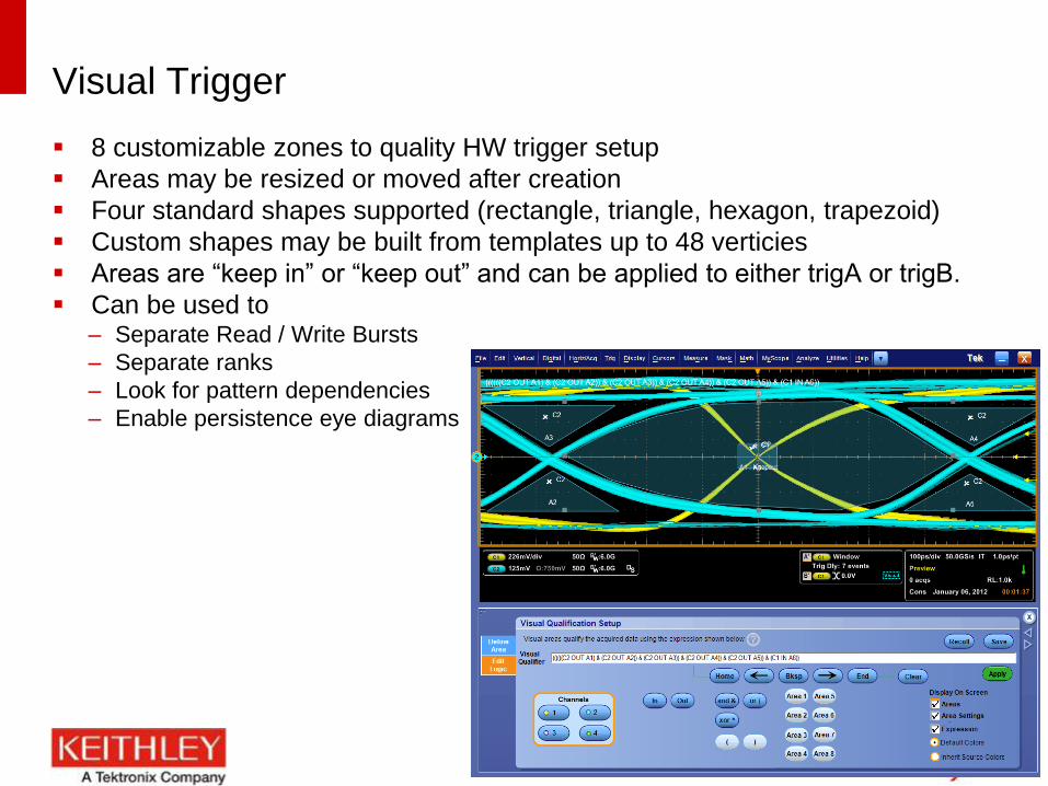
Visual Trigger
8 customizable zones to quality HW trigger setup
Areas may be resized or moved after creation
Four standard shapes supported (rectangle, triangle, hexagon, trapezoid)
Custom shapes may be built from templates up to 48 verticies
Areas are “keep in” or “keep out” and can be applied to either trigA or trigB.
Can be used to – Separate Read / Write Bursts
– Separate ranks
– Look for pattern dependencies
– Enable persistence eye diagrams

Visual Trigger Used For DQ Pattern Detection 010000X Pattern
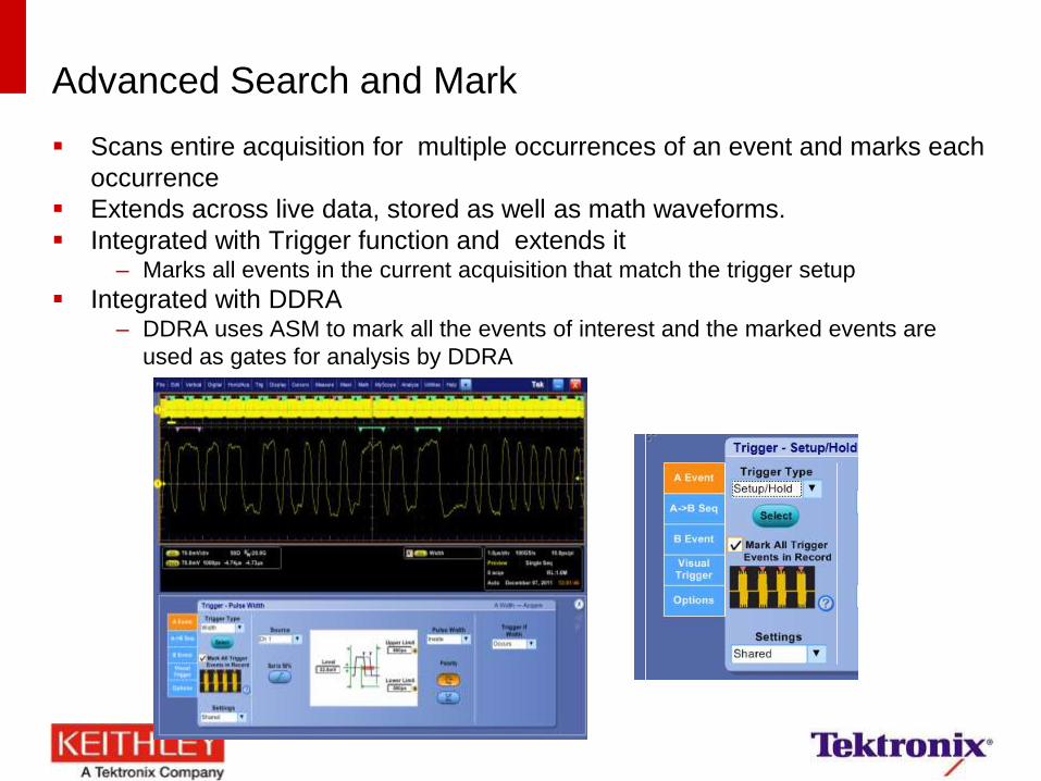
Advanced Search and Mark
Scans entire acquisition for multiple occurrences of an event and marks each
occurrence
Extends across live data, stored as well as math waveforms.
Integrated with Trigger function and extends it – Marks all events in the current acquisition that match the trigger setup
Integrated with DDRA – DDRA uses ASM to mark all the events of interest and the marked events are
used as gates for analysis by DDRA
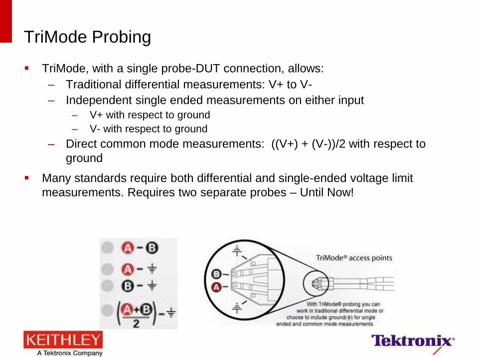
TriMode Probing
TriMode, with a single probe-DUT connection, allows:
– Traditional differential measurements: V+ to V-
– Independent single ended measurements on either input
– V+ with respect to ground
– V- with respect to ground
– Direct common mode measurements: ((V+) + (V-))/2 with respect to
ground
Many standards require both differential and single-ended voltage limit
measurements. Requires two separate probes – Until Now!
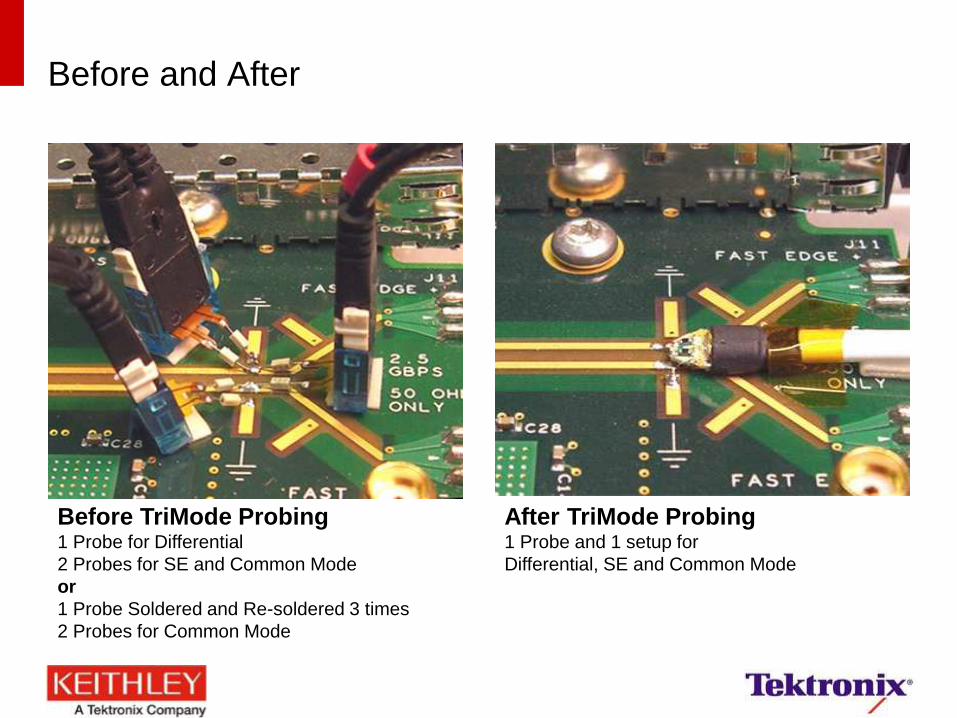
Before and After
Before TriMode Probing 1 Probe for Differential
2 Probes for SE and Common Mode
or
1 Probe Soldered and Re-soldered 3 times
2 Probes for Common Mode
After TriMode Probing 1 Probe and 1 setup for
Differential, SE and Common Mode
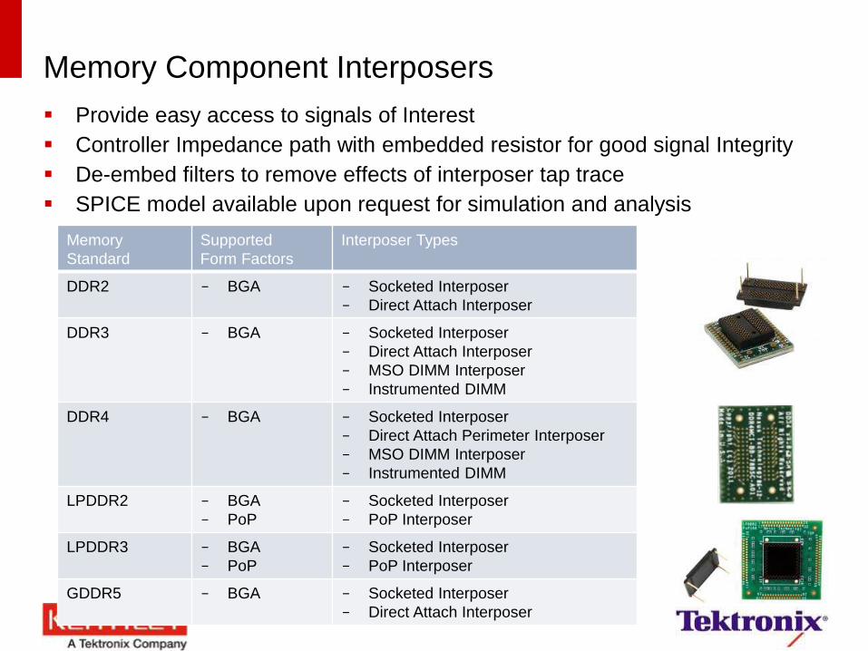
Memory Component Interposers
Memory
Standard
Supported
Form Factors
Interposer Types
DDR2 - BGA - Socketed Interposer
- Direct Attach Interposer
DDR3 - BGA
- Socketed Interposer
- Direct Attach Interposer
- MSO DIMM Interposer
- Instrumented DIMM
DDR4 - BGA - Socketed Interposer
- Direct Attach Perimeter Interposer
- MSO DIMM Interposer
- Instrumented DIMM
LPDDR2 - BGA
- PoP
- Socketed Interposer
- PoP Interposer
LPDDR3 - BGA
- PoP
- Socketed Interposer
- PoP Interposer
GDDR5 - BGA
- Socketed Interposer
- Direct Attach Interposer
Provide easy access to signals of Interest
Controller Impedance path with embedded resistor for good signal Integrity
De-embed filters to remove effects of interposer tap trace
SPICE model available upon request for simulation and analysis
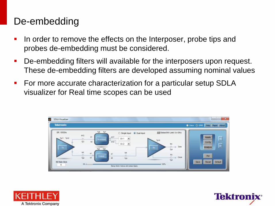
De-embedding
In order to remove the effects on the Interposer, probe tips and
probes de-embedding must be considered.
De-embedding filters will available for the interposers upon request.
These de-embedding filters are developed assuming nominal values
For more accurate characterization for a particular setup SDLA
visualizer for Real time scopes can be used
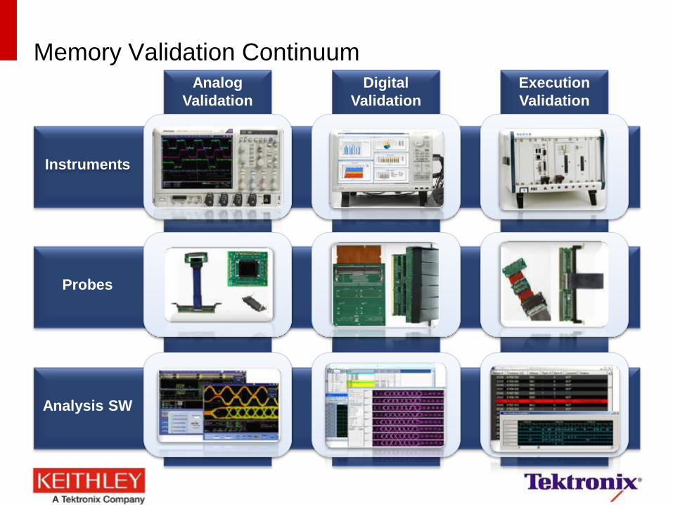
Memory Validation Continuum
Analysis SW
Analog
Validation
Instruments
Probes
Digital
Validation
Execution
Validation
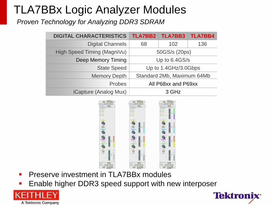
TLA7BBx Logic Analyzer Modules Proven Technology for Analyzing DDR3 SDRAM
50GS/s (20ps)
Memory Depth
TLA7BB3 TLA7BB4 TLA7BB2 DIGITAL CHARACTERISTICS
Digital Channels
High Speed Timing (MagniVu)
Deep Memory Timing
State Speed
68 102 136
Up to 6.4GS/s
Up to 1.4GHz/3.0Gbps
Standard 2Mb, Maximum 64Mb
Probes All P68xx and P69xx
iCapture (Analog Mux) 3 GHz
Preserve investment in TLA7BBx modules
Enable higher DDR3 speed support with new interposer
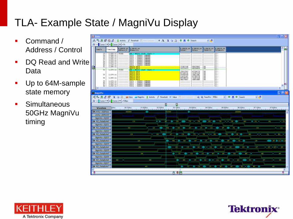
TLA- Example State / MagniVu Display
Command /
Address / Control
DQ Read and Write
Data
Up to 64M-sample
state memory
Simultaneous
50GHz MagniVu
timing
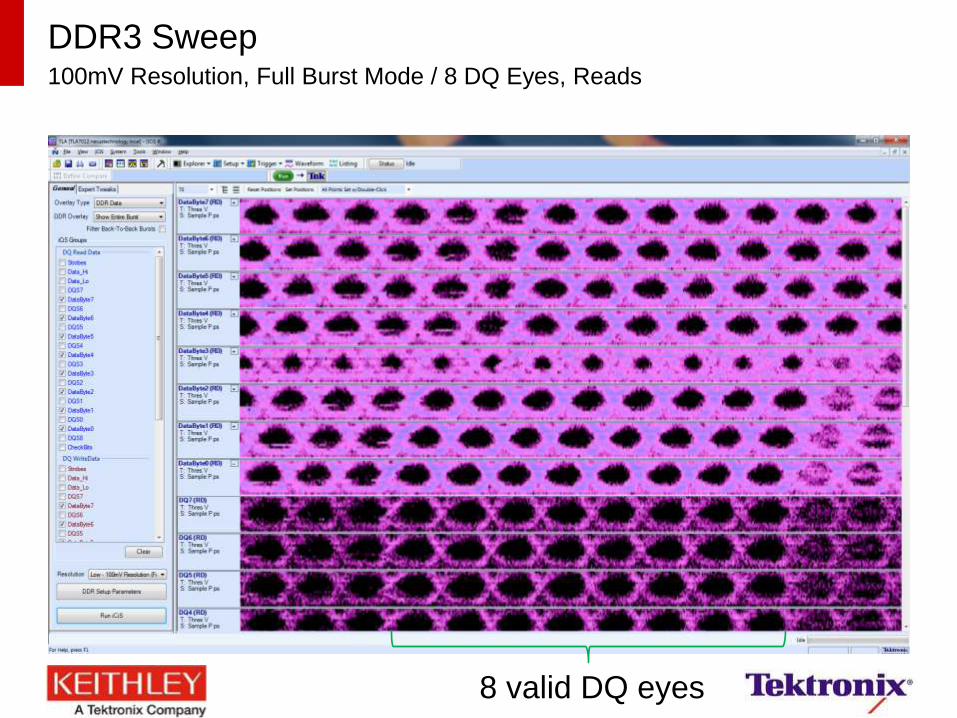
DDR3 Sweep 100mV Resolution, Full Burst Mode / 8 DQ Eyes, Reads
8 valid DQ eyes
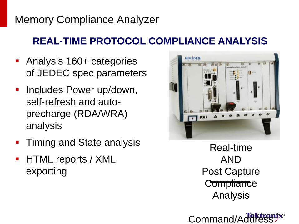
Memory Compliance Analyzer
REAL-TIME PROTOCOL COMPLIANCE ANALYSIS
Real-time
AND
Post Capture
Compliance
Analysis
Command/Address
Analysis 160+ categories
of JEDEC spec parameters
Includes Power up/down,
self-refresh and auto-
precharge (RDA/WRA)
analysis
Timing and State analysis
HTML reports / XML
exporting

Thanks!