Embed Size (px)
Citation preview

Projekt współfinansowany ze środków Unii Europejskiej w ramach Europejskiego Funduszu Społecznego
ROZWÓJ POTENCJAŁU I OFERTY DYDAKTYCZNEJ POLITECHNIKI WROCŁAWSKIEJ
Wrocław University of Technology
Electronics, Photonics, Microsystems
Leszek Golonka (Chapters 1-5)
Karol Malecha (Chapters 6-9)
CERAMIC MICROSYSTEMS
Wrocław 2011

Wrocław University of Technology
Electronics, Photonics, Microsystems
Leszek Golonka (Chapters 1-5) Karol Malecha (Chapters 6-9)
CERAMIC MICROSYSTEMS
Developing Engine Technology
Wrocław 2011

Copyright © by Wrocław University of Technology
Wrocław 2011
Reviewer: Andrzej Dziedzic
ISBN 978-83-62098-29-3
Published by PRINTPAP Łódź, www.printpap.pl

i
CERAMIC MICROSYSTEMS
Contents i
Chapter 1. Thick film materials and processing 1.1
1.1. Introduction 1.1
1.2. Thick film manufacturing process 1.2
Substrate 1.3
Paste 1.4
Design 1.9
Screen 1.10
Screen printing 1.11
Firing process 1.12
Trimming process 1.14
Assembling and packaging 1.15
References 1.17
Chapter 2. LTCC (Low Temperature Cofired Ceramics)
materials and processing 2.1
2.1. Introduction 2.1
2.2. Multichip Module (MCM) 2.1
2.3. LTCC manufacturing process 2.3
2.4. Properties of cofired LTCC module 2.6
2.5. Design of LTCC module 2.9
2.6. Integrated passive components 2.12
2.7. Microwave application 2.16
2.8. LTCC processes for microsystems 2.17
References 2.18
Chapter 3. Sensors, actuators and microsystems –
fundamentals and classification 3.1
3.1. Introduction 3.1
3.2. Fundamentals 3.1
3.3. Physical and chemical sensors 3.3
3.4. LTCC microsystems – general information 3.5
3.5. MEMS, MOEMS packaging 3.7

ii
3.6. Heating and cooling systems 3.9
3.7. Energy source 3.11
References 3.14
Chapter 4. LTCC and thick film physical sensors 4.1
4.1. Temperature sensors 4.1
Thermocouples 4.1
RTD (Resistive Temperature Device) sensors 4.3
Thermistors 4.6
4.2. Flow sensors 4.10
4.3. Pressure sensors 4.13
4.4. Force sensors 4.17
4.5. Proximity sensor 4.17
References 4.19
Chapter 5. LTCC and thick film chemical sensors
5.1. Humidity sensors 5.1
Ceramic humidity sensors 5.4
5.2. Gas sensors 5.7
Semiconductor gas sensors 5.7
Electrochemical gas sensors 5.10
References 5.11
Chapter 6. Foundation of microfluidics 6.1
6.1. Introduction 6.1
6.2. Basic terms and equations of fluid dynamics 6.2
Reynolds number 6.2
The continuity equation 6.4
Navier-Stokes equation 6.6
Pressure drop 6.8
6.3. Scaling laws in microfluidics 6.10
References 6.16

iii
Chapter 7. Technology of the LTCC-based
microfluidic systems 7.1
7.1. Introduction 7.1
7.2. Laser processing of green ceramic tapes 7.3
7.3. Mechanical machining of green ceramic tapes 7.7
7.4. Hot embossing 7.9
7.5. Jet vapor etching 7.12
7.6. Photolithographic patterning 7.14
7.7. Photoformable LTCC tapes 7.15
7.8. Sacrificial volume material 7.18
7.9. Low pressure lamination methods 7.24
References 7.29
Chapter 8. Bonding techniques of the LTCC with
different materials 8.1
8.1. Introduction 8.1
8.2. LTCC-Si 8.1
8.3. LTCC-glass 8.5
8.4. LTCC-PDMS 8.8
8.5. LTCC-ceramic 8.11
References 8.12
Chapter 9. LTCC-based microfluidic systems 9.1
9.1. Introduction 9.1
9.2. Microvalves and micropumps 9.1
Piezoelectric action 9.1
Piezoelectric valve 9.4
Piezoelectric pump 9.6
Electromagnetic actuation 9.8
Electromagnetic valve 9.9
Electromagnetic pump 9.11
9.3. Ceramic micromixers 9.13
Magneto-hydro-dynamic (MHD) mixer 9.15
Serpentine passive mixres 9.17
9.4. Microreactors 9.20
Enzymatic microreactor for urea determination 9.20

iv
PCR (Polymerase Chain Reaction) microreactor 9.23
9.5. Electrochemical sensors 9.26
Potentiometric sensor with ion selective (ISE) based array 9.26
PDMS/ceramic module for potentiometic determination
of urea 9.29
Amperometric sensor for continuous glucose monitoring 9.31
Electrochemical sensor for heavy metal determination
in biological and environmental fluids 9.34
9.6. Optical sensors 9.35
LTCC-based microfluidic sensor for absorbance
measurement 9.35
LTCC-based fluorescent sensor 9.37
LTCC-based microfluidic system with
optical detection 9.39
References 9.40

1.1
Chapter 1
Thick film materials and processing
1.1. Introduction
In the thick film technology, the individual layer is deposited by
screen printing on the insulator substrate. The thick film material is referred
to as an ink or paste. The paste contains three main components: a functional
phase (metal or oxide powder) which determines the electrical properties of
the fired films, a binder (glass powder) which provides adhesion between the
fired film and the substrate, and the organic vehicle which enables the screen
printing process. After deposition the films are dried and then fired at the
temperature around 850oC.
The screen print technique has been known for few thousand years. It
was used in China to decorate ceramics with gold patterns. In electronics the
technique was used for the first time around 1930 to make a silver electrode
on a capacitor. The first thick film hybrid device was made in 1945 in the
USA.
The mass production of thick film hybrid microelectronics started
around 1960. Thirty years later the technology was also used for production
of MCM (Multichip Module), sensors, actuators and microsystems. The
pastes were deposited not only on alumina substrates but also on green
ceramic tape to form a multilayer LTCC (Low Temperature Cofired
Ceramics) module [1-6].
Advantages of thick film technology:
- low cost,
- simple automation,
- inexpensive production of short series,
- miniaturisation,
- very good electrical properties,
- production of various components,
- resistance to high temperatures,
- good mechanical properties.
1.1

1.2
Disadvantages:
- dimensions,
- no active components,
- tolerance.
Thick film components:
- conductor,
- resistor,
- capacitor,
- inductor,
- sensor,
- actuator,
- microsystem,
- thermistor,
- varistor,
- heaters,
- . . .
This chapter will focus on the basic technology for thick film
materials with an emphasis on composition, design, processing and properties
of the thick film components.
1.2. Thick film manufacturing process
After printing, the pastes are typically dried at 150oC for 10 min to
remove the volatile solvent component of the vehicle. Next, the film is fired
in a tunnel oven with a temperature profile which includes 10 min at a peak
temperature of 850oC and an overall firing cycle time from 30 to 60 min. The
process is shown in Fig. 1.1. Precious metal conductors are fired in air while
copper requires firing in nitrogen. The print, dry, and fire steps are repeated to
fabricate the final structure. The process can be automated for low cost, high
volume production.
Typical parameters of thick films:
film thickness 5-15 m (dielectric 50 m)
width (min) 100 m (min 15 m)
1.2
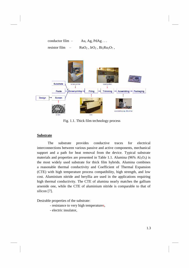
1.3
conductor film – Au, Ag, PdAg . . .
resistor film – RuO2 , IrO2 , Bi2Ru2O7 ,
Fig. 1.1. Thick film technology process
Substrate
The substrate provides conductive traces for electrical
interconnections between various passive and active components, mechanical
support and a path for heat removal from the device. Typical substrate
materials and properties are presented in Table 1.1. Alumina (96% Al2O3) is
the most widely used substrate for thick film hybrids. Alumina combines
a reasonable thermal conductivity and Coefficient of Thermal Expansion
(CTE) with high temperature process compatibility, high strength, and low
cost. Aluminium nitride and beryllia are used in the applications requiring
high thermal conductivity. The CTE of alumina nearly matches the gallium
arsenide one, while the CTE of aluminium nitride is comparable to that of
silicon [7].
Desirable properties of the substrate:
- resistance to very high temperatures,
- electric insulator,
1.3

1.4
- good thermal conductivity,
- proper CTE,
- surface flatness.
Substrate materials:
- alundum ceramics ( 96% Al2O3 ),
- AlN ceramics,
- BeO ceramics,
- enamel steel.
Table 1.1.
Summary of typical substrate materials
Paste
The paste contains three components: the main ingredient (functional
phase - metal or oxide powder) which determines the electrical properties of
the fired films, the binder (glass powder) which provides adhesion between
the fired film and the substrate, and the organic vehicle which enables the
screen printing process.
• Main ingredient (powdered functional phase):
conductive paste - Au, Ag, PdAg, ...
resistive paste - RuO2, IrO2, Bi2Ru2O7, ... .
Ceramics AlN Al2O3 BeO LTCC
Thermal Conductivity [W/m.K] 140-170 10-35 150-250 2-3
Coefficient of Thermal Expansion
(CTE) [10-6
/K]
4.6 7.3 5.40 5.8-7
Resistivity [.m] 4x10
11 > 10
14 10
13-10
15 > 10
12
Electrical permittivity (1 MHz) 10 9.5 7 5.9-9
1.4

1.5
• Glass (powdered glass phase):
PbO - B2O3 - SiO2 (or without PbO
• Organic vehicle:
solvent - viscosity (η) correction,
- reduction of surface tension,
- improving of wetting,
Ethylcellulose - adhesion to substrate after drying at the temperature
of 120oC.
All the components are mixed together. The paste productivity
depends on the quality of the paste, screen density and emulsion thickness.
Typical productivity is presented in
Table 1.2.
Table 1.2.
Paste productivity
Substrate coverage
[cm2/g]
Screen
[mesh]
Au
Pt-Au
Pd-Ag
Pt-Ag
Cu
Dielectric paste
45 ÷ 55
40 ÷ 45
65 ÷ 75
55 ÷ 65
65 ÷ 75
75 ÷ 85
325
200
200
200
240
200
Emulsion thickness: 10 ÷ 12 μm
Mesh –number of openings in 1 inch length
Conductor paste
The functional phase for conductors may be made of gold, palladium-
gold, platinum-gold, silver, palladium-silver, platinum-silver or copper. The
1.5

1.6
choice of the metallurgy depends on bondability or solderability of the wire,
environmental requirements, electrical conductivity and the cost [7]. A
comparison of various conductors is provided in Table 1.3.
Thick film conductor sheet resistance R = /d = 2 ÷ 100 m/□
where: - resistivity of film
d – film thickness
Materials fired in air: Au, PtAu, PdAu, Ag, PtAg, PdAg
(disadvantage: Au – dissolution in solder,
Ag – diffusion)
Material fired in nitrogen: Cu
Application: electrode, connection, soldering pads etc.
Requirements: low resistivity, adhesion, solderability, ... .
Table 1.3.
Properties of thick film conductors
Material R [m/] Material R [m/]
Au 2 10 PdAg 10 50
Pt-Au 15 100 Pt 50 80
Pd-Au 10 100 Cu* 2
Ag 2 10 Ni* 7 40
* firing in nitrogen
Resistor paste
Resistor systems are formulated with ruthenium (RuO2, Bi2Ru2O7,
etc.) or IrO2 doped glasses. Thick film resistor pastes provide a wide range of
resistance values by varying the concentration of the glass. The most
important resistor properties are sheet resistance (R), Temperature
Coefficient of Resistance (TCR) and stability. There are resistor systems for
1.6

1.7
general purposes, high voltage, potentiometric and sensor (high Gauge
Factor) applications.
Sheet resistance (R)
R = /d = 10 108 [/],
Temperature Coefficient of Resistance (TCR)
TCR = (R2 – R1)x106/[R1(T2 – T1)] = (50300) [ppm/K]
where: R1 – resistance at temperature T1
R2 - resistance at temperature T2
Cold TCR (T1 = 25oC, T2 = -55
oC)
Hot TCR (T1 = 25oC, T2 = 125
oC)
Piezoresistive properties - Gauge Factor (GF)
GF = (R/R)/(l/l) = 10 20
where: R – resistance change
R - initial resistance
l - length change
l - initial length
Parameters of thick film resistors:
R 1/ ÷ 100 M/
TCR ± 50 ppm/°C ÷ ± 300 ppm/°C
d – film thickness 5 ÷ 15 μm
tolerance (without trimming) ± 20%
Pr (alumina substrate 96% Al2O3) 8 W/cm2
Pp (for substrate surface) 0.25 W/cm2
S – noise index -35 ÷ +35 dB
1.7

1.8
Pr - max power density dissipated by the resistor (area of the resistor
film)
Pp - max power density dissipated by the substrate (area of the
substrate).
Fig. 1.2. Typical characteristic of piezoresistor [7]
Dielectric paste
Dielectric pastes are used for insulation between conductor layers,
formation of capacitors and encapsulation of the hybrid substrate. Dielectric
for insulation are typically glass-ceramics compositions with low dielectric
constant, low dissipation factor, high voltage strength, high insulation
1.8

1.9
resistance and a CTE matched to the substrate. Thick film parallel plate
capacitors are not widely used [7].
Other pastes: solder, thermistor, varistor, magnetoresistor, sensor, etc.
Design
The screen printing process is capable of resolving lines and spaces
down to 100 µm or less. However, in high volume production it is advisable
to restrict the resolution [7]. Typical thick film resistors guidelines are
presented in Fig. 1.3, Fig. 1.4 and Table 1.4.
Fig. 1.3. Thick film resistor
dimensions [7]
Fig. 1.4. Laser trim cut modes [7]
1.9

1.10
D1 250 (125)
D2 250 (125)
D3 250 (200)
D4 500 (375)
D5 750 (500)
D6 500 (500)
(i) – in brackets minimal value
Screen
The screen is fabricated by stretching a fine stainless steel mesh screen
over a frame and epoxying the mesh to the frame. The screen dimensions are
presented in Fig. 1.5. The most important screen parameters are: mesh angle,
screen frame size, screen mesh size and screen tension. The photosensitive
emulsion is applied by one of two methods: by using liquid emulsion or by
using a photosensitive film. The emulsion is exposed to the ultraviolet light to
get the desired circuit pattern. The screen covered with emulsion is shown in
Fig. 1.6. It is also possible to buy ready made screens, both with and without
the emulsion.
Fig. 1.5. Screen dimensions
1.10
Table 1.4.
Thick film resistor dimensions (vide Fig. 1.3)
Dimension Length [m] Remarks
L 1000 (500) 0.5<L/W<5 (0.3<L/W<10)
W width depends on tolerance and power

1.11
Fig. 1.6. Screen covered with the emulsion [8]
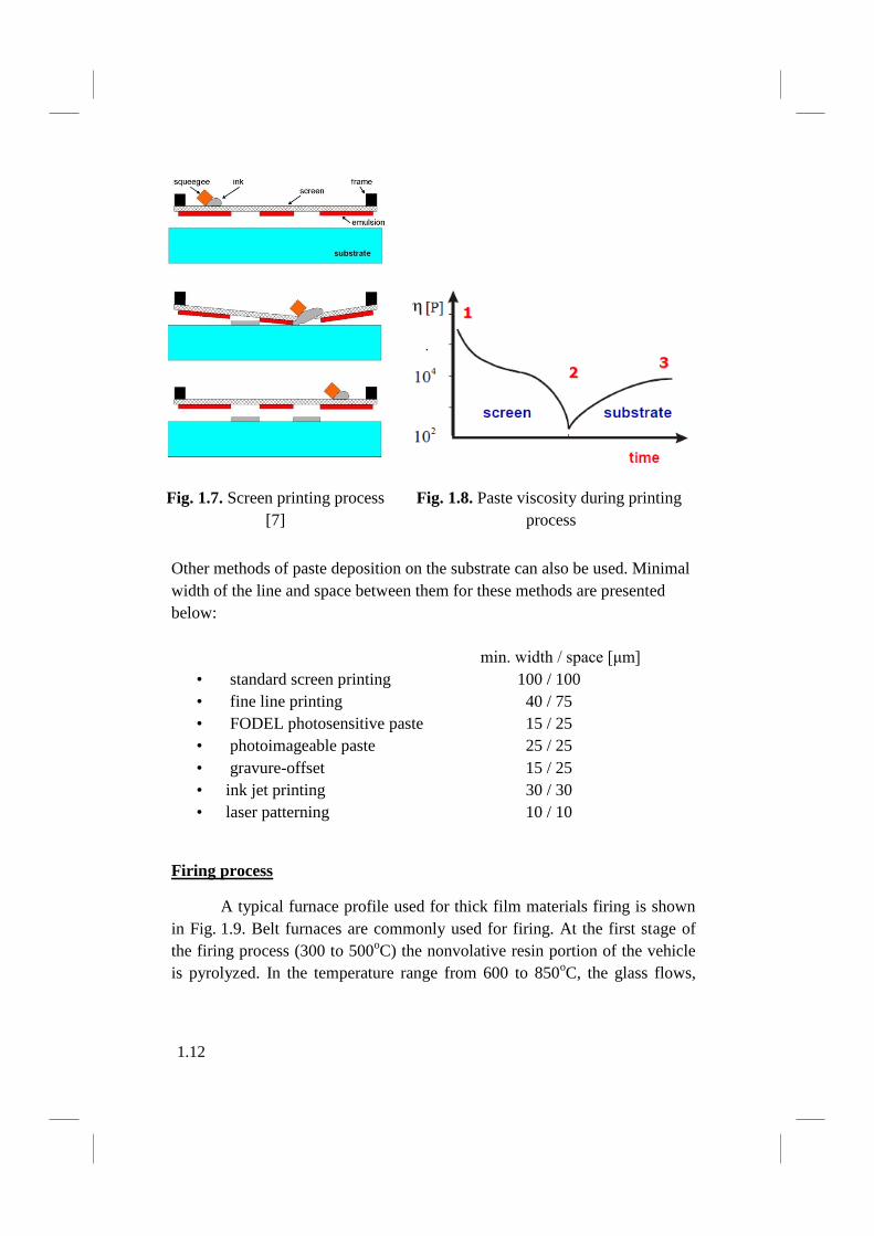
Screen printing
The purpose of screen printing is to deposit a film of ink with
predictable dimension on a substrate. The individual layer is deposited as
illustrated in Fig. 1.7. Screen printing determines the accuracy of the printed
pattern. The important process parameters in screen printing include screen
printer setup (snap-off distance, speed, pressure), squeegee (hardness, shape),
screen (wire diameter, mesh opening size, emulsion chemistry and thickness,
screen tension) and paste rheology. The change in paste viscosity during the
printing process is shown in Fig. 1.8.
1.11
1.12
Fig. 1.7. Screen printing process
[7]
Fig. 1.8. Paste viscosity during printing
process
Other methods of paste deposition on the substrate can also be used. Minimal
width of the line and space between them for these methods are presented
below:
min. width / space [μm]
• standard screen printing 100 / 100
• fine line printing 40 / 75
• FODEL photosensitive paste 15 / 25
• photoimageable paste 25 / 25
• gravure-offset 15 / 25
• ink jet printing 30 / 30
• laser patterning 10 / 10
Firing process
A typical furnace profile used for thick film materials firing is shown
in Fig. 1.9. Belt furnaces are commonly used for firing. At the first stage of
the firing process (300 to 500oC) the nonvolative resin portion of the vehicle
is pyrolyzed. In the temperature range from 600 to 850oC, the glass flows,
1.12
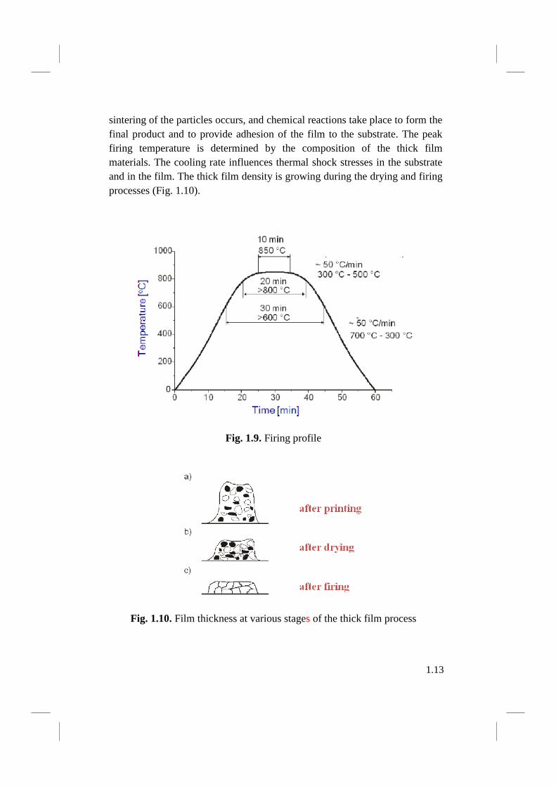
1.13
sintering of the particles occurs, and chemical reactions take place to form the
final product and to provide adhesion of the film to the substrate. The peak
firing temperature is determined by the composition of the thick film
materials. The cooling rate influences thermal shock stresses in the substrate
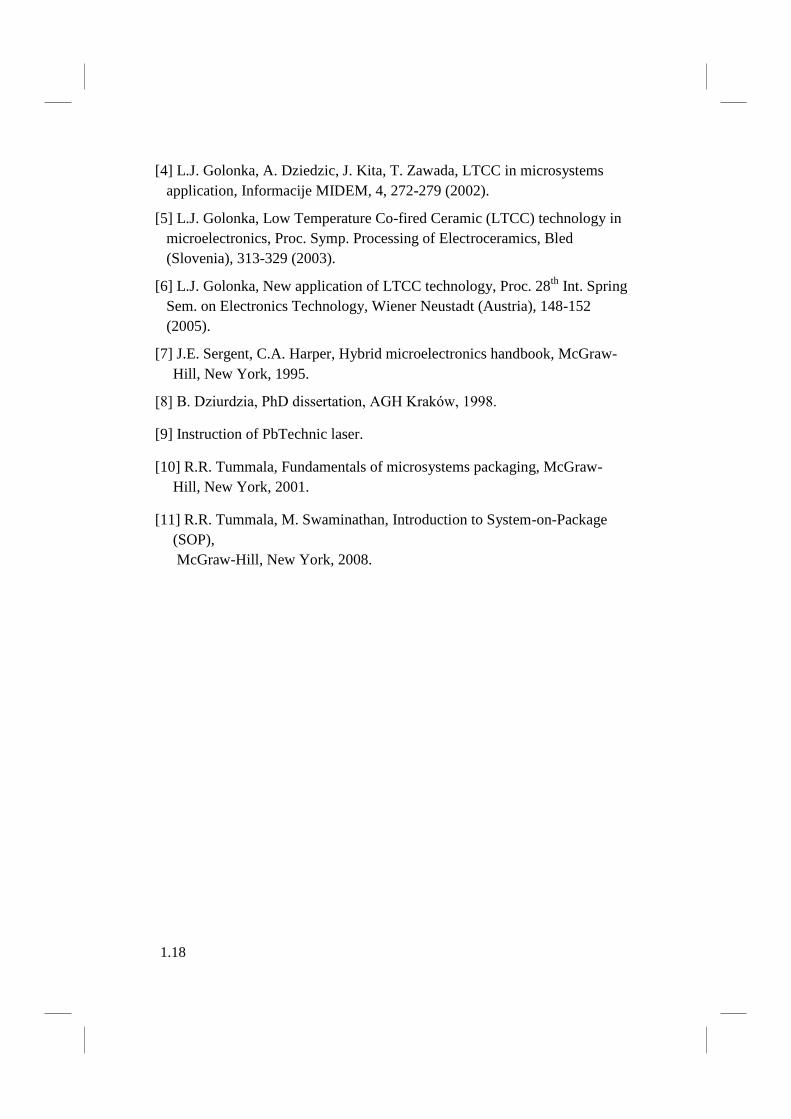
and in the film. The thick film density is growing during the drying and firing
processes (Fig. 1.10).
Fig. 1.9. Firing profile
Fig. 1.10. Film thickness at various stages of the thick film process
1.13

1.14
Trimming process
Thick film resistors are required to meet sometimes tolerances of
±0.1%. Because of the complex nature of the resistor they cannot be fired
with the required tolerance. Very often the tolerance after firing is equal to
±20%. Therefore, the resistors are trimmed to the target value by removing a
part of the resistor film with a laser. The film absorbs the light, which causes
it to heat rapidly and vaporise. Decreasing the effective width of the resistor
increases the resistance value (Fig. 1.11). A neodymium-doped yttrium
aluminium garnet (Nd:YAG) laser operating at 1064 nm wavelength is
typically used. The laser parameters (Q-rate, power, cut speed) must be
experimentally determined. The laser trims can be classified into four major
types of cut: plunge, double plunge, L and serpentine (Fig. 1.12).
Fig. 1.11. Resistance distribution a) after firing, b) after trimming
1.14

1.15
Fig. 1.12. Type of laser trim cuts [9]
Assembling and packaging
Various assembly technologies are used for the electro-mechanical
attachment of discrete components to the substrate. The attachment can be
realised by soldering or wire bonding methods. Moreover, polymer adhesives
can be used for the attachment. Various assembling methods are shown in
Fig. 1.13 and Fig. 1.14.
1.15

1.16
Fig. 1.13. Various assembling methods [10]
Fig. 1.14. Various assembling methods [Europractice EU Project]
Proper operating conditions can be maintained by encasing the thick
film circuit in a protective package. A significant performance improvement
can be achieved by optimising the electronic package. The device requires the
electronic package that can match its performance in electrical, mechanical
1.16

1.17
and thermal aspects. The packaging of the device or microsystem should
ensure the following conditions: proper operating temperature, protection
from humidity and contaminants, mechanical support, good thermal
management [10,11]. Various packaging levels are presented in Fig. 1.15.
Fig. 1.15. Electronics packaging levels [10]
References
[1] P.E. Garrou, I. Turlik, Multichip Module technology handbook, McGraw-
Hill, New York, 1998.
[2] L.J. Golonka, Zastosowanie ceramiki LTCC w mikroelektronice, Oficyna
Wydawnicza Politechniki Wroclawskiej, Wroclaw 2001.
[3] L.J. Golonka, Application of thick films in LTCC technology, Informacije
MIDEM,
vol. 29 (4), 169-175 (1999).
1.17
1.18
[4] L.J. Golonka, A. Dziedzic, J. Kita, T. Zawada, LTCC in microsystems
application, Informacije MIDEM, 4, 272-279 (2002).
[5] L.J. Golonka, Low Temperature Co-fired Ceramic (LTCC) technology in
microelectronics, Proc. Symp. Processing of Electroceramics, Bled
(Slovenia), 313-329 (2003).
[6] L.J. Golonka, New application of LTCC technology, Proc. 28th
Int. Spring
Sem. on Electronics Technology, Wiener Neustadt (Austria), 148-152
(2005).
[7] J.E. Sergent, C.A. Harper, Hybrid microelectronics handbook, McGraw-
Hill, New York, 1995.
[8] B. Dziurdzia, PhD dissertation, AGH Kraków, 1998.
[9] Instruction of PbTechnic laser.
[10] R.R. Tummala, Fundamentals of microsystems packaging, McGraw-
Hill, New York, 2001.
[11] R.R. Tummala, M. Swaminathan, Introduction to System-on-Package
(SOP),
McGraw-Hill, New York, 2008.
1.18
2.1
Chapter 2
LTCC (Low Temperature Cofired Ceramics) materials and
processing
2.1. Introduction
The Low Temperature Cofired Ceramic (LTCC) technology started at
eighties of the last century as one of the technologies used for production of
Multichip Modules (MCM). Multilayer MCM substrate is capable of
supporting several chips in one package [1]. At the beginning, the technology
was mostly used for production of high volume microwave devices. Recently,
the LTCC is applied to the production of sensors, actuators, microreactors,
microsystems, MEMS and MOEMS packages [2-7]. The LTCC module
exhibits very good electrical and mechanical properties, high reliability and
stability as well as possibility of making three-dimensional (3D) integrated
microstructures. The technology is well established both for low volume, high
performance applications (military, space) and high volume low cost
applications (wireless communication, car industry). A great advantage of
LTCC technology is the low temperature of cofiring (in comparison with
standard ceramic processes). It enables the use of typical thick film materials.
2.2. Multichip Module (MCM)
Multichip Module technology is the most efficient packaging
technology. It has the features that enable size reduction and higher speed
performance to be obtained by eliminating individual packages and their
parasitics. The semiconductor devices are attached to the MCM substrate by
using various interconnection methods such as wire bonding, tape automated
bonding or flip chip [1]. Depending on the method of fabrication, MCMs
have been divided into three basic groups, shown in Fig. 2.1:
- MCM-C are built using either multilayer cofired ceramic substrates or
thick film interconnection technology on ceramic substrate,
2.1

2.2
- MCM-D have interconnection structure built by deposition of thin
film metals and dielectric materials over silicon, diamond, ceramic or
metal substrate,
- MCM-L have substrates built by using the most advanced PWB
(Printing Wired Boards) technology
Examples of the MCM-D and MCM-C modules are presented in Fig. 2.2.
Ceramic technology (MCM-C) for multilayer modules can be divided into
three major categories:
- Thick film multilayer process (TFM),
- High temperature cofired alumina processes (HTCC),
- Low temperature cofired ceramic/glass based processes (LTCC).
Fig. 2.1. Various Multichip Modules
LTCC modules have a number of advantages over HTCC (High
Temperature Co-fired Ceramics) structures used before. The cofiring process
takes place at lower temperature (LTCC at 8500C; HTCC at 1600
0C1800
0C)
and therefore well established thick film materials and processing can be
adopted to this technology. Metals with higher conductivity like gold, silver
2.2

2.3
or copper replace tungsten or molybdenum used in HTCC modules. Two
basic materials are used in the LTCC tape fabrication – alumina filled glasses
and glass-ceramics. The basic LTCC ceramic tape can be modified to produce
dielectric materials with different electrical and physical properties. The
coefficient of thermal expansion can be adopted to match alumina, gallium
arsenide, or silicon. Standard thick film conductor, resistor and capacitor
materials are used in LTCC circuits as buried (2D or 3D) or surface
components. Lower mechanical strength and thermal conductivity are the
main disadvantages of LTCC, in comparison with HTCC. The advantages of
the LTCC technology in comparison with other MCM-C techniques are
presented in Fig. 2.3.
Fig. 2.2. Examples of MCM-D and MCM-C (LTCC) modules
2.3. LTCC manufacturing process
The LTCC multilayer structure is presented in Fig. 2.4. The module consists
of dielectric tapes, connecting vias, external and internal conductors and
passive components (resistors, capacitors, inductors). The components are
made by a standard screen printing method. Thick or thin film components
can be made on the top and bottom surfaces of the fired module. Additional
2.3

2.4
circuits and elements are added on the top and the bottom of the structure
using various assembling methods. Moreover, the module can integrate
sensors, actuators, channels, optoelectronic components, heating and cooling
systems.
Fig. 2.3. Advantages of LTCC technology
Fig. 2.4. Cross-section of a LTCC module (author: T. Zawada)
2.4

2.5
The conductors and passive components are printed by a standard
screen printing method. After printing the cavities are made using automatic
punch or laser. The finished sheets are stacked on a laminating plate and
laminated in an uniaxial or isostatic laminator. The typical laminating
parameters are 200 atm at 70oC for 10 minutes. After the lamination process
the structures are cofired in two steps (Fig. 2.7). The first step, typically at
around 500oC is the binder burnout step. The second, at 850
oC, makes the
ceramic material densify. The firing process is carried out in one
programmable oven or in two separate ovens. The processes which occur
during the cofiring process are described in [7,8]. The second firing step can
be made in an ordinary thick film furnace. The fired parts usually shrink by
12% in the x- and y- directions and by about 17% in the z-direction. After
cofiring the thick film or thin films components can be made on the top and
bottom surfaces and additional active or passive elements can be added using
various assembling methods. Thin film deposition process is a very expensive
one, and the surface of the fired tape must be extremely smooth for good
adhesion [9]. In the end the structures are singulated using dicing saw,
ultrasonic cutting or laser cutting.
Fig. 2.5. LTCC process flow
2.5

2.6
Fig. 2.6. Tape casting process
Fig. 2.7. Cofiring profile
2.4. Properties of cofired LTCC module
LTCC materials are based either on crystallizable glass [10,11] or a
mixture of glass (CaO-B2O3-SiO2, … ) and ceramics, for example, alumina,
silica or cordierite (Mg2Al4Si5O18) [12,13]. Typical properties of LTCC
materials are presented in Table 2.1.
Shrinkage variations and poor thermal conductivity are the main
limitations of LTCC technology. To eliminate shrinkage, Heraeus produces
new tape HeraLockTM
2000 (Table 2.2).
2.6

2.7
Table 2.1. Typical properties of the LTCC materials
Property \ Tape DuPont
DP 951
DuPont
DP 943
Ferro
A6M
ESL
41110-
7-C
Heraeus
CT 2000
Heraeus
HL2000
Electrical
Dielectric
constant
7.85 7.5 5.9 4.34.7 9.1 7.3
Dissipation
factor
0.0045 0.001 0.002 0.004 0.002 0.0026
Breakdown
voltage
[V/25m]
> 1000 > 1000 > 1000 > 1500 > 1000 > 800
Insulation
resistance
[cm]
> 1012
> 1012
> 1012
> 1012
> 1013
> 1013
Dimensional
Thickness –
green [µm]
50, 112,
162, 250
125 125, 250 125 25, 50,
97, 127,
250
131
Thickness –
fired [µm]
42, 95,
137, 212
112 92, 185 105 20, 40,
77, 102,
200
8794
Shrinkage x,y
[%]
12.70.3 9.50.3 14.80.2 130.5 10.60.3 0.160.24
Shrinkage z [%] 15.00.5 10.30.3 270.5 161 20.01.5 32
Camber
[µm/mm]
< 2 < 2 < 2 < 1
Colour blue light blue white blue light blue light blue
Thermal
CTE [ppm/K] 5.8 4.5 7 6.4 5.6 6.1
Thermal cond.
[W/m.K]
3 4.4 2 2.5÷3 3 3
Mechanical
Density [g/cm3] 3.1 3.2 2.45 2.3 2.45 2.45
Flexural
Strength [MPa]
320 230 > 170 310 > 200
Young’s
Modulus [GPa]
152 92
2.7

2.8
The tape exhibits near-zero shrinkage (less than 0.2% with variation in the
shrinkage less than 0.014%) in the x and y directions upon firing. The tape
shows about 30% z-axis total shrinkage through firing [14-18]. HeraLockTM
2000 is a lead and cadmium free formulation with the properties appropriate
for RF applications, automotive modules and general purpose packaging. For
optoelectronic applications it is possible to make buried optical channels and
fibers which remain undistorted after firing. Low x-y shrinkage also enables
firing the tape with embedded passive devices such as ferrite transformers or
chip capacitors. HL2000 exhibits a nearly dry (glass free) ceramic surface
after firing without negative effect on conductor solderability.
LTCC’s thermal conductivity of 2.0 2.5 W/mK is a limitation to the
structures dissipating many watts of power. The most common method of
increasing heat transfer in the z-axis is the application of thermal vias [19].
The thermal vias are the holes that are filled with silver or gold and are placed
beneath the hot components. The thermal conductivity in the z- axis can be
increased up to 120 W/mK or 70 W/mK in the case of Ag and Au,
respectively [3].
Generations of LTCC modules
I generation - conductive paths and vias
II generation - conductive paths and vias
- passive components (MCIC)
III generation - conductive paths and vias
- passive components (MCIC)
- sensors and actuators
- microsystems
Advantages and disadvantages of LTCC technology
Advantages:
• very good electrical and mechanical properties,
• high stability,
• integration of various components,
• 3-dimensional (3D) structures,
• various applications,
• low cost.
2.8

2.9
Disadvantages:
• dimension,
• no active components,
• thermal conductivity.
Applications of LTCC technology:
• Multichip Modules
• microwave modules
• passive components
• sensors and actuators
• photonic modules
• smart packages
• fuel cells
• microreactors
• microsystems
2.5. Design of LTCC module
Some basic DuPont information on design rules are presented in Figs.
2.8 - 2.10 and Table 2.2 [20].
Fig. 2.8. Interconnect terminology [20]
2.9

2.10
Fig. 2.9. Design of vias in LTCC module [20]
Fig. 2.10. Design of resistor and ground plane in the LTCC module [20]
2.10

2.11
Table 2.2.
Design parameters [20]
Feature Typical Demonstrated capability
# tape layers 20 100
Substrate x, y dimension
(green) [mm]
200 x 200 450 x 450
Substrate thickness [mm]
< 100 x 100 0.625 0.095
> 100 x 100 1.25 0.500
Lines / spaces
Co-fired [µm] 125 / 125 50 / 50
Post fired [µm] 175 min 75
Via diameter 1:1 aspect ratio < 1:1 aspect ratio
Via cover pad 2x via dia 1x via dia
Via pitch (min) 3x via dia 2x via dia
Via center to center 3x via dia 0x via dia
Via metal to line
spacing [µm]
125 min no pad
Via stagger (min) 2x via dia no stagger
Thermal via diameter/pitch [µm]
Option I 250 / 750 thermal slots
Option II 375 / 1000 -
Space from gnd/pwr/sig
to part edge [µm]
250 min 0
Gnd/pwr plane coverage 70% gridded 100%
Gnd/pwr plane openings for feed throughs [mm]
Thermal via 1.75 1.25
Signal via 1.25 0.625
2.11

2.12
Post fired resistors
Length 750 250
Width 750 250
Overlap 125 125
Product Thickness (green) [µm]
951C2 50
951PT, 951AT 114
951P2, 951A2 165
951PX, 951AX 254
951RT release tape 127
2.6. Integrated passive components
The LTCC module can integrate electrical, optical, gas and fluidic
networks with electronic measurement, control and signal conditioning
circuits. Passive electronic components are embedded inside the LTCC
module or made on the top. The properties of the passive components are
presented below:
R Resistors - sheet resistance surface 10 /sq. to 1 M/sq.
(tolerances of 1% to 2%)
buried 10 /sq. to 100 k/sq.
(tolerances of 10% to 20%)
L Inductors - inductance 5 nH to 200 nH
C Capacitors – capacitance 70 pF/cm2 using standard tape
(accuracy of 10%-20%)
up to 25 nF/cm2 using K700 dielectric
The resistor can be made on the top of the LTCC module as
“postfired” (print on fired ceramics) or cofired (print on green tape).
Embedded resistors are printed on green tapes and cofired with the module.
2.12

2.13
Various methods of resistor trimming are shown in Fig. 2.11. The resistors
can be made as planar (2D) or 3-dimensional (3D) as presented in Fig. 2.12.
The designs of capacitors and inductors are shown in Figs. 2.13 - 2.18.
Microwave transmission lines in LTCC are presented in Fig. 2.19.
Fig. 2.11. Resistors in LTCC [21]
Fig. 2.12. Planar (2D) and 3-dimensional (3D) resistors
2.13

2.14
Fig. 2.13. Passive LTCC components (capacitor and inductor)
Fig. 2.14. Basic design of capacitors in
LTCC [21]
Fig. 2.15. Capacitor model for
wide-band simulations [21]
2.14

2.15
Fig. 2.16. Inductors in LTCC [21]
Fig. 2.17. Inductor design in LTCC and
a photo of 4.5 turns buried coil [21]
Fig. 2.18. Fine-line laser patterned
top layer inductor spiral
2.15

2.16
a) b) c)
Fig. 2.19. Transmission lines in LTCC a) RF/high-speed-line, b) microwave-
stripline, c) waveguide [21]
2.7. Microwave application
Microwave circuits were the first application of the LTCC technology.
This area of LTCC products is still the biggest one. Various LTCC
microwave devices are presented in Fig. 2.20.
Fig. 2.20. Microwave application of LTCC [22].
2.16

2.17
Murata is one of the biggest producers of LTCC microwave
components. It has delivered over 950 million pieces of multilayer LTCC
based components in the years 1989 - 2000 (LC filters, baluns, couplers, chip
antennas, RF diode SW) [22]. The parameters of Murata components are
presented below:
Substrate length and width max 10 mm
thickness 1 – 2 mm
layer thickness 50 m (25, 100, 150 m
optional)
Conductor line width/space 100 m / 100 m
via diameter 130 m
Resistor range 50 - 100 k
tolerance 5%
TCR 300 ppm/K
Buried capacitor C 1 pF/mm2 x layer
tolerance 5%
TCC 80 20 ppm/K
Strip line inductance impedance 100 max
spiral or radial 100 nH max
2.8. LTCC processes for microsystems
New materials for tape casting (high k, piezoelectric, piroelectric etc.)
and special LTCC techniques are developed for the fabrication of LTCC
microsystems. These techniques are connected with the following processes:
fine line patterning, micromachining of LTCC tapes, lamination, making of
cavities, holes and channels, bonding of LTCC tapes to other materials.
2.17

2.18
The LTCC techniques for ceramic microsystems are described in Chapter 7
(laser processing and mechanical machining of green ceramic tapes, hot
embossing, jet vapor etching, photolithographic patterning, photoformable
LTCC tapes, sacrificial volume material, low pressure lamination methods).
LTCC can be joined to various materials by different techniques. These
methods are described in Chapter 8.
References
[1] P.E. Garrou, I. Turlik, Multichip Module technology handbook, McGraw-
Hill, New York, 1998.
[2] L.J. Golonka, Zastosowanie ceramiki LTCC w mikroelektronice, Oficyna
Wydawnicza Politechniki Wroclawskiej, Wroclaw 2001.
[3] L.J. Golonka, Application of thick films in LTCC technology, Informacije
MIDEM, vol. 29 (4), 169-175 (1999).
[4] L.J. Golonka, A. Dziedzic, J. Kita, T. Zawada, LTCC in microsystems
application, Informacije MIDEM, 4, 272-279 (2002).
[5] L.J. Golonka, Low Temperature Co-fired Ceramic (LTCC) Technology in
microelectronics, Proc. Symp. Processing of Electroceramics, Bled
(Slovenia), 313-329 (2003).
[6] L.J. Golonka, New application of LTCC technology, Proc. 28th
Int. Spring
Sem. on Electronics Technology, Wiener Neustadt (Austria), 148-152
(2005).
[7] C.B. DiAntonio, D.N. Bencoe, K.G. Ewsuk, “Characterization and control
of Low Temperature Co-fire Ceramic (LTCC) sintering”, Proc. IMAPS
Conf. on Ceramic Interconnect Technology, Denver 2003, pp. 160-164.
[8] T.J. Garino, “The co-sintering of LTCC materials”, Proc. IMAPS Conf. on
Ceramic Interconnect Technology, Denver 2003, pp. 171-176.
[9] T. Pisarkiewicz, A. Sutor, W. Maziarz, H. Thust, T. Thelemann, “Thin
film gas sensors on Low Temperature Cofired Ceramics”, Proc. European
Microelectronics Packaging and Interconnection Symposium, Prague,
2000, pp. 399-403.
[10] A.A. Shapiro, D.F. Elwell, P.Imamura, M.L. MeCartney, “Structure-
property relationships in low-temperature cofired ceramic”, Proc. 1994
Int. Symp. on Micr ISHM-94, Boston, 1994, pp. 306-311.
2.18

2.19
[11] J.-H. Jean, C.-R. Chang, “Camber development during cofiring Ag-based
low-dielectric-constant ceramic package”, J. Mater. Res., 12, (10), (1997),
pp. 2743-2750.
[12] R.E. Doty, J.J. Vajo, “A study of field-assisted silver migration in low
temperature cofirable ceramic”, Proc. 1995 Int. Symp. on Micro ISHM-95,
Los Angeles, 1995, pp. 468-474.
[13] C.-J. Ting, C.-S. Hsi, H.-J. Lu, “Interactions between ruthenium-based
resistors and cordierite-glass substrates in low temperature co-fired
ceramics”, J. Am. Ceram. Soc., 83, (12), (2000), pp. 2945-2953.
[14] P. Barnwell, E. Amaya, F. Lautzenhiser, J. Wood, “HeraLock TM 2000
self-constrained LTCC tape – beneficts and applications”, Proc. IMAPS
Nordic Annual Conference, Stockholm (Sweden), Sept. 2002, pp. 250-256.
[15] M. Ehlert, B. Spenser, F. Lautzenhiser, E. Amaya, ”Characterization of
unrestrained zero shrink LTCC material for volume production of RF
LTCC modules”, Proc. Int. Symp. on Microel. IMAPS USA, Denver, Sept.
2002.
[16] F. Lautzenhiser, E. Amaya, P. Barnwell, J. Wood, „Microwave module
design with HeraLockTM
HL2000 LTCC”, Proc. Int. Symp. on Microel.
IMAPS USA, Denver, Sept. 2002.
[17] Q. Reynolds, P. Barnwell, “Self constrained LTCC technology –
HeraLock”, Proc. MicroTech 2003, London, Feb. 2003, pp. 3-38.
[18] C. Modes, M. Neidert, F. Herbert, Q. Reynolds, F. Lautzenhiser, P.
Barnwell, „A new constrained sintering LTCC technology for automotive
electronic applications“, Proc. 14th
European Microel. and Pack. Conf.,
Friedrichshafen (Germany), June 2003, pp. 118-122.
[19] R. Kandukuri, Y. Liu, M. Zampino, W. Kinzy Jones, „High density
thermal vias in Low Temperature Cofire Ceramic (LTCC)”, Proc. Int. Symp.
on Microel. IMAPS USA, Denver, Sept. 2002.
[20]http://www2.dupont.com/MCM/en_US/assets/downloads/prodinfo/LTCC_Desi
gnGuide.pdf
[21] L.J. Golonka, H. Thust, Applications of LTCC ceramics in microwave,
Proc. 9th
Int. Conf. MIXDES’2002, Wroclaw (Poland), June 2002, pp. 101-
110.
[22] Chiang S-K, Radio frequency packaging, Proc. IEMT/IMC, Japan 2000,
pp. 367-370.
2.19

2.20
2.20

3.1
Chapter 3
Sensors, actuators and microsystems - fundamentals and
classification
3.1. Introduction
The transducer that converts a non-electrical quantity into an electrical
signal is called a sensor, and the type of transducer that converts an electrical
signal into a non-electrical quantity is called an actuator. A reduction in the
size of a sensor leads to an increase in its applicability and a lower cost [1].
The microsensors are made using conventional thin film, thick film and
LTCC technologies as well as silicon micromachining. This Chapter focuses
on fundamental information on physical and chemical sensors as well as
packaging, heating, cooling and energy source LTCC modules for
microsystems.
3.2. Fundamentals
Sensor terminology
A sensor may be regarded as a system with an input x(t) and output
y(t). The input signal can be of physical, chemical or biological nature. The
output signal is electrical or optical (Fig. 3.1).
The input-output curve y=f(x) is called sensor conversion function
(Fig. 3.2). The ideal sensor has a linear output signal y(t) which
instantaneously follows the input signal x(t), hence
y(t) = S x(t)
The slope S of the input-output curve has a constant value for a linear
sensor and is called the sensitivity. In practice, the sensor conversion function
is not linear and the sensitivity does not have a constant value (Fig. 3.3).
The sensor can not respond instantaneously to a change in the input
signal but requires some time to reach its steady-state value (Fig. 3.4). The
rise (and fall) of an output signal from a sensor is exponential with a
characteristic time constant τ. The characteristic time constant τ can be related
3.1

3.2
to the physical properties of the system. Often the time taken for the sensor
signal to reach 90% of its final value is referred to as the t90 time or
sometimes the response time. It is desirable for the value of the t90 to be less
than a few seconds.
Fig. 3.1. Schematic representation of an electrical sensor
Fig. 3.2. Sensor conversion function (author: R. Jachowicz)
3.2

3.3
Fig. 3.3. Sensor sensitivity Sx (R. Jachowicz)
Fig. 3.4. Transient response of an ideal sensor system [1]
3.3. Physical and chemical sensors
The classification of the sensors can be made in different manner. It
can be made on the base of the input signal, technology, signal processing,
energy conversion or the effect applied in signal conversion [1,2].
Sensor classification
Input signal:
- physical
- chemical
- biological (biosensor)
3.3

3.4
Technology:
- conventional
- thick film, LTCC
- thin film
- semiconductor processing
Signal processing:
- electronic
- optic
Energy conversion:
- generation (self–exciting)
- parametric (modulating)
Effect applied in signal conversion:
- piezoelectric
- piezoresistive
- magnetoresistive
- pyroelectric
- thermoelectric
- polarymetric
- . . . .
Depending on the input signal the sensors are divided into two groups:
physical and chemical sensors:
Physical sensors
- temperature
- pressure
- force
- air flow
- heat flow
- radiation
- fluid level
- inclination
- . . . .
3.4

3.5
Chemical sensors
- humidity
- pH
- ion concentration
- gas concentration
- . . .
Very important parameters of the sensors are as follows:
- sensitivity
- selectivity
- stability (reproducibility)
- protection against environment
- system compatibility
- cost
Due to the possibility of very good electronic conditioning of the
signal the sensitivity is not a big problem nowadays. Selectivity is still
enormous problem for gas sensors. Stability and protection against
environment does not pose any problems for physical sensors. We can protect
them very well from the ambient atmosphere. However, it is a great problem
for chemical sensors. In this case the sensitive material of the sensor has to be
exposed to the environment. There is still a real problem for all sensors with a
time drift and a calibration.
3.4. LTCC microsystems – general information
The Low Temperature Cofired Ceramic (LTCC) technology has been
used at the beginning to produce a multilayer substrate for packaging
integrated circuits and microwave devices. Recently, the LTCC was also
applied to the production of sensors, actuators and microsystems because of
3.5

3.6
its very good electrical and mechanical properties, high reliability and
stability as well as possibility of making three-dimensional (3D) integrated
microstructures [3-5]. A great advantage of the LTCC technology is the low
temperature of cofiring. It enables the use of the typical thick film materials.
A great variety of these materials with different electrical properties are used
to make a network of conductive paths in a package and to integrate other
electronic components, sensors, actuators, microsystems, cooling and heating
systems in one module. With the use of this technology it is also possible to
produce MEMS and MOEMS packages.
LTCC sensors and actuators
- temperature sensor
- pressure sensor
- gas sensor
- heating system
- cooling system
- flow sensor
- proximity sensor
- microvalve
- micropump
LTCC technology advantages and disadvantages:
Advantages
- simple and inexpensive technology
- low cost and short time of a new design prototyping
- sensor integration
- resistance to environment and high temperature
- system integration (sensor, actuator, electronics)
- microsystems
Disadvantages
- dimension
- no active components
- . . .
3.6

3.7
LTCC physical sensors:
- temperature
- gas and liquid flow
- pressure
- force
- proximity sensor
- heat flow
- radiation
- fluid level
- inclination
- . . .
LTCC chemical and biochemical sensors
- humidity
- pH
- ion concentration
- gas concentration
- glucose
- urea
- . . .
3.5. MEMS and MOEMS packaging
The LTCC technology can be used for making a “smart” packaging
for MEMS and MOEMS microsystems [6-9]. The package not only protects
mechanically the microsystem. The integrated electronics, cooling or heating
system and sensors can be made inside the LTCC multilayer module.
Moreover, electrical, optical, fluid and gas connections can be realized via a
channel made inside the module. The LTCC packaging is presented in Fig.
3.5.
The acceleration chip sensor using the differential capacitive method,
bonded to the LTCC package is shown in Fig. 3.6. The metallized LTCC
wafer was bonded simultaneously with the Si-wafer and glass wafer. Joining
of the metallized LTCC multilayer and silicon in a wafer process without any
3.7

3.8
intermediate bonding layers is possible. Further chip packaging includes
joining the chip and LTCC; some functions will be performed in the chip,
some in the LTCC. The overall manufacturing cost may decrease because of
the reduced packaging size [9]. The photonic LTCC package is presented in
Fig. 3.7.
Fig. 3.5. The LTCC packaging for MEMS and MOEMS [6]
Fig. 3.6. Cross-section of an acceleration chip sensor and bonded layers
(anodic bonding) [9]
The LTCC can be applied to photonic integration. A 3D LTCC
structure with the grooves, cavities, holes, bumps and alignment fiducials for
passive alignment of photonic devices was presented by Kautio and Karioja
3.8

3.9
[10,11]. The thermal vias and liquid cooling channels were used for high
power laser cooling (Fig. 3.7). Moreover, high speed integrated circuits as
well as millimeter wave circuits can be integrated into the LTCC substrate.
Fig. 3.7. Photonic package [10,11]
3.6. Heating and cooling systems
The LTCC module can integrate the heating and cooling systems [12-
14]. The proper temperature of the sensor or ceramic microreactor is very
important. For example, the sensitivity of the gas sensor depends strongly on
the temperature and its distribution on the surface of the gas sensitive
material. The LTCC gas heater is shown in Fig. 3.8 and the microfluidic
3.9

3.10
mixer with the heater and temperature sensor is presented in Fig. 3.9. The rate
of the chemical reaction between two fluids in the ceramic microreactor is
temperature sensitive. The special design of the heater allows one to get a
uniform temperature distribution in the reaction area.
The cooling system is very important in the device with high density
of power. The model LTCC module with a laser diode soldered to the
package with the cooling system is shown in Fig. 3.10a. The temperature near
the laser diode with and without the cooling system is presented in Fig. 3.10b.
Fig. 3.8. Gas sensor hot-plate LTCC heater [14]
Fig. 3.9. LTCC microfluidic mixer with heater and temperature sensor [13]
3.10

3.11
(a)
(b)
Fig. 3.10. a) Scheme of a model LTCC package with a laser diode and water
cooling system [10], b) temperature near the laser diode measured with a
thermistor (b) [15]
3.7. Energy source
The LTCC technology can be used successfully for producing
integrated fuel cell system (sensors, mixer, channels, cavities, conditioning
electronics) [16,17]. Fuel cells are an alternative way to conventional
batteries for supplying electronic products (mobile phones, notebooks) with
electrical energy. The miniature fuel cells have a high efficiency and a high
power density due to the direct conversion of chemical to electrical energy.
Fig. 3.11 shows the schematic configuration of the fuel cell system [16]. At
the anode the oxidation of hydrogen takes place. The hydrogen ions move
through the electrolyte to the cathode. The electrons are directed through an
outer electrical circuit to the cathode (Fig. 3.12).
Fig. 3.11. Schematic configuration of the fuel cell system [16]
3.11

3.12
Fig. 3.12. Principle reaction in fuel cell [16]
PEM - Proton Exchange Membrane
MEA - Membrane Electrode assembly
GDL – Gas Diffusion Layer
Fig. 3.13. 3D picture of the Proton Exchange Membrane Fuel Cell (PEMFC)
system [16]
3.12

3.13
The general structure of the LTCC fuel cell system is shown in Fig.
3.13. The whole device contains the fuel cell system with the charging circuit
and the voltage converter plus a metal hydride and/or a hydrogen pressure
tank. The properties of the four cell system in series connection are shown in
Fig. 3.14. At the USB terminal the DC/DC converter transforms the varying
output voltage into a constant 5 V DC. The main parameters of the fuel cell
system are summarized in Table 3.1 [16].
Fig. 3.14. U-I-P characteristics of PEMFC system [16]
Table. 3.1.
Characteristic points of the fuel cell system [16]
3.13

3.14
References
[1] J.W. Gardner, Microsensors, Wiley,New York, 1995.
[2] M. Prudenziati, Thick film sensors, Elsevier Science B. V., Amsterdam,
1994.
[3] L.J. Golonka, A. Dziedzic, J. Kita, T. Zawada, LTCC in microsystems
application, Informacije MIDEM, 4, 2002, 272-279.
[4] L.J. Golonka, New application of LTCC technology, Proc. 28th
Int. Spring
Seminar on Electronics Technology, Wiener Neustadt (Austria), 2005, pp.
148-152.
[5] L.J. Golonka, Technology and applications of Low Temperature Cofired
Ceramic (LTCC) based sensors and microsystems, Bulletin of the Polish
Academy of Sciences, Vol. 54 (2), 2006, pp. 223-233.
[6] M. Schuenemann et al., MEMS modular packaging and interfaces, Proc.
50th
Electronic Com. & Technol. Conf., Las Vegas (USA), 2000, pp. 681-
688.
[7] L.J. Golonka, A. Dziedzic, J. Dziuban, J. Kita, T. Zawada, LTCC package
for MEMS device, Optoelectronic and Electronic Sensors V, W. Kalita,
Editor, Proceedings of SPIE, 5124, 2003, pp. 115-119.
[8] E. Műller et al., Advanced LTCC-packaging for optical sensors, Proc. 14th
European Microel. and Pack. Conf., Friedrichshafen (Germany), 2003, pp.
19-24.
[9] E. Müller et al., Development and processing of an anodic bondable
LTCC tape, Proc. 15th European IMAPS Conf. Brugge, 2005, pp. 313-318
[10] K. Kautio et al., Precision alignment and cooling structures for photonic
packaging on LTCC, Proc. IMAPS Cer. Interconnect Technology Conf.,
Denver 2004
[11] P. Karioja et al., LTCC toolbox for photonic integration, Proc. CICMT
Conference, Denver (USA) 2006.
[12] J. Kita, Ph.D. Dissertation, Wroclaw University of Technology, 2003.
[13] T. Zawada, Ph.D. Dissertation, Wroclaw University of Technology,
2004.
[14] J. Kita, F. Rettig, R. Moos, K-H. Drűe, H. Thust, Hot-plate gas sensors –
are ceramics better?, Proc. 2005 IMAPS/AcerS 1st Int. Conf. and Exhib.
on Ceramic Interconnect and Cer. Microsystem Technologies (CICMT),
Baltimore (USA), 2005, pp. 343-348.
3.14

3.15
[15] K. Keränen et al., Fiber pigtailed multimode laser module based on
passive device alignment on an LTCC substrate. IEEE Tr Advanced
Packaging 2006
[16] A. Goldberg, U. Partsch, M. Stelter, A charging unit based on Micro-
PEM-Fuel cells in LTCC technology, Proc. CICMT Conference, Denver
2007, pp. 338-343.
[17] A. Michaelis, Application of ceramic technology for cost effective
manufacturing of small fuel cell systems, Proc. CICMT Conference,
Denver 2007, pp. 333-337
3.15

3.16
3.16

4.1
Chapter 4
LTCC and thick film physical sensors
4.1. Temperature sensors
Thermal sensors are used to measure various heat related quantities,
such as temperature, heat flux and heat capacity. Temperature is perhaps the
most important process parameter and about 40% of all solid-state sensors are
thermal sensors [1]. Temperature is important in chemical processes where
reaction-rate is usually exponentially temperature dependent according to the
Arrhenius relationship. Temperature is a fundamental parameter in many
processes and it may need to be measured, compensated for or even
controlled in some manner. It is also exploited as a secondary sensing
variable in non-thermal microsensors, for example a gas sensor or a flow
sensor. The most important temperature sensors used in thick film and LTCC
microsystems are thermocouples, Resistive Temperature Devices (RTD) and
thermistors. There is a broad variety of temperature sensor applications:
- temperature measurements inside device,
- gas and fluid flow sensor,
- heater with temperature control sensors,
- heat flow sensor,
- . . .
Thermocouples
An thermoelectric force is generated when a circuit consists of two
different metals and the junctions are held at different temperatures. Fig. 4.1
shows the basic arrangement where a junction of two materials is held at a
temperature TA while a second reference junction is held at a temperature TB.
A thermoelectric potential ΔV is generated across the junctions. The device is
referred to as a thermocouple and the thermoelectric effect is known as the
Seebeck effect. The effect was discovered in 1821.
4.1

4.2
Fig. 4.1. Basic circuit of a thermocouple temperature sensor [1]
The Seebeck effect in metals (and alloys) is small. The thermoelectric
e.m.f is normally associated with combined changes in the Fermi energy EF
and the diffusion potential. The Fermi level effect VF is given by [1]:
VF = PS T = EF / q
where q is the electron charge. The Fermi level of a metal depends upon its
temperature T and the density of states N(E), and is given by
EF(T) = EF(0) – π2 k
2 T
2 d(ln N(E))/6dE
where EF(0) is the Fermi level of the metal at absolute zero and k is
Boltzmann’s constant.
PA = V / T PS = PB – PA Vr = (PB – PA) T
PA , PB – Seebeck coefficient of metal A and B
V - thermoelectric potential (open circuit voltage)
T – junction temperature (TA) – reference temperature (TB)
PS - Seebeck coefficient measured by a thermocouple
Vr - generated thermoelectric force (e.m.f)
EF - Fermi level
N(E) - density of states
4.2

4.3
Fig. 4.2 shows the typical thermoelectric e.m.f.’s E generated by
standard wire thermocouples. Thick/thin film thermopiles made on the LTCC
substrate is presented in Fig. 4.3 (a). They consist of a number of PdAg/TSG
thermocouples deposited on DP 951 ceramics. The 0.25 mm wide PdAg
tracks were screen printed and fired at 1123 K. Second arms were made by
magnetron sputtering of tantalum-antimony-germanium alloy (TSG).
Temperature [
oC]
Fig. 4.2. Thermoelectric e.m.f.’s E generated by
standard wire thermocouples [2]
RTD (Resistive Temperature Device) sensors
The resistive temperature detectors rely on the temperature
dependence of metals and alloys. This phenomenon may be exploited in
temperature sensors made of metal wires, thin and thick films. The RTD
exhibits high positive temperature coefficients of resistance (TCR).
4.3
4.4
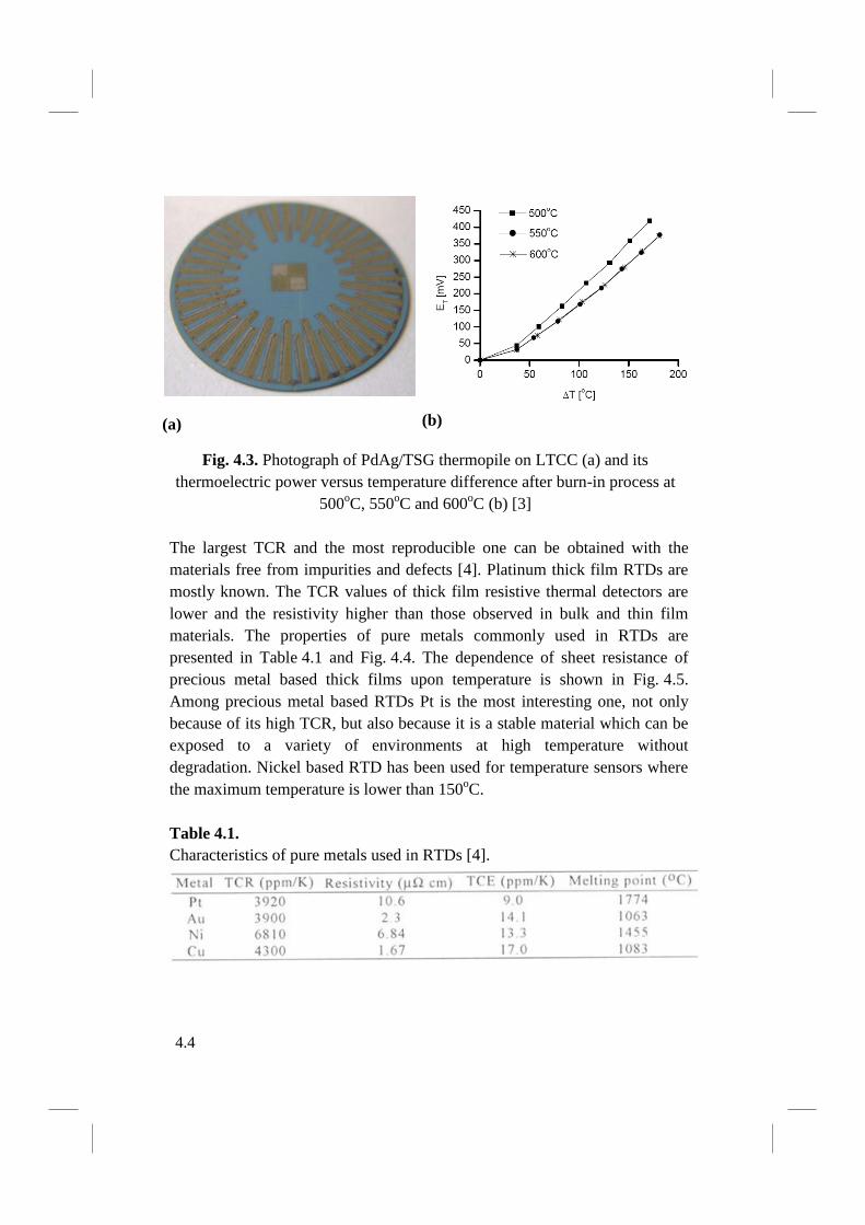
(a)
(b)
Fig. 4.3. Photograph of PdAg/TSG thermopile on LTCC (a) and its
thermoelectric power versus temperature difference after burn-in process at
500oC, 550
oC and 600
oC (b) [3]
The largest TCR and the most reproducible one can be obtained with the
materials free from impurities and defects [4]. Platinum thick film RTDs are
mostly known. The TCR values of thick film resistive thermal detectors are
lower and the resistivity higher than those observed in bulk and thin film
materials. The properties of pure metals commonly used in RTDs are
presented in Table 4.1 and Fig. 4.4. The dependence of sheet resistance of
precious metal based thick films upon temperature is shown in Fig. 4.5.
Among precious metal based RTDs Pt is the most interesting one, not only
because of its high TCR, but also because it is a stable material which can be
exposed to a variety of environments at high temperature without
degradation. Nickel based RTD has been used for temperature sensors where
the maximum temperature is lower than 150oC.
Table 4.1.
Characteristics of pure metals used in RTDs [4].
4.4

4.5
Fig. 4.4. Relative resistance changes of pure metals versus temperature [2]
Fig. 4.5. Sheet resistance of precious metal based thick films [3]
4.5

4.6
The resistance dependence of Pt, PdAg and PtAu thick films RTDs
buried in LTCC module upon temperature is shown in Fig. 4.6.
Fig. 4.6. Relative resistance changes versus temperature of RTD LTCC buried
components: Pt (TCR = 2500 ppm/K), PdAg (TCR = 430 ppm/K), PtAu (TCR
= 380 ppm/K) [5]
Thermistors
Thermistors (Fig. 4.7) are made from semiconducting ceramic
materials (e.g. sulphides, selenides, oxides of Ni, Mn, Cu etc.). The
resisitivity of a typical thermistor is much higher than that of a metal
thermoresistor. The TCR of NTC (Negative Temperature Coefficient)
thermistor is negative and highly non-linear as shown in Fig. 4.8. The plot
shows the material resistances relative to its ice-point resistance in order to
normalize the values and compare them with platinum and nickel RTD [1].
The temperature characteristic of NTC thermistor can be described by
equation:
R = A exp (B/T)
where: A – constant
B – thermistor constant
4.6

4.7
Some metal oxide materials possess a positive temperature coefficient
of resistance. These PTC thermistors have very different current-voltage
characteristics (Fig. 4.9).
Fig. 4.7. Topology of single thermistor
Fig. 4.8. Typical plot of resistance vs. temperature of a NTC thermistor and
RTD elements (Ni and Pt) [1]
4.7

4.8
Fig. 4.9. Current-voltage characteristics of NTC and PTC thermistors [1]
The design of thick film thermistor determines the required values of
the thermistor constant B and the resistance R. The temperature characteristic
(constant B) is strictly related to the thermistor composition. The resistance
depends on the resistivity of thermistor material and the thick film component
design. The requirement of resistance can be met by an appropriate choice of
the thermistor structure. It relies on three main configurations: planar, comb
and sandwich (Fig. 4.10) [4]. For the same thermistor paste the planar type
gives the highest resistance while the sandwich type the lowest one. The
resistance R of the thermistor is related to the component design according to
the following equations:
planar and comb types R = ρ L/(D W) = Rs L/W
sandwich type R = ρ D/S = Rs D2/S (D = L)
Rs = ρ/D
where ρ - resistivity
Rs - sheet resistance
D - thickness
W - electrode width
L - distance between electrodes
S - electrode area.
4.8

4.9
Fig. 4.10. Designs of thick film thermistors [4]
The properties of thick film thermistors manufactured by DuPont and
ESL are presented in Tables 4.2 and 4.3, respectively.
Table 4.2.
Parameters of DuPont 5090D PTC thick film thermistors [6].
There are many applications of the temperature sensors, for example:
- heat flow sensors,
- gas and liquid flow sensors,
- heaters,
4.9

4.10
- temperature measurements inside a multilayer LTCC structure,
- solarimeters,
- measurements of laser power.
Some applications are described below.
Table 4.3.
Parameters of Electro-Science Laboratories PTC and NTC thick film
thermistors [7].
PTC-2600 SERIES
NTC-2100 SERIES
4.2. Flow sensors
The LTCC gas flow sensor is described by Gongora Rubio [8]. The
basic sensor structure consists of a thick film resistive heater and two
thermistors printed on a thermally isolated bridge in a cavity (Fig. 4.11). The
sensor measures the temperature in the bridge using two thermistors. The
temperature difference is related to the flow in the cavity. The thermistors are
4.10

4.11
screen-printed on the bridge together with the ruthenium-based resistor for
the heater. Fig. 4.12 depicts various layers of the basic sensor schematically
and Fig. 4.11 is a SEM micrograph of the device cross-section. Temperature
difference vs. flow at different values of the heater current Ip, as a parameter
is displayed in Fig. 4.13.
Fig. 4.11. Schematics: flow sensor layers and cross-section [8]
Fig. 4.12. Cross-section of a basic
flow sensor [8]
Fig. 4.13. Delta T vs. flow with
parameter Ip [8]
4.11

4.12
A gas flow sensor made on the LTCC tube is described by Smetana
[9]. The principle of work is similar to the case of Gongora Rubio flow
sensor. The prototype of the calorimetric flow sensor and its temperature
characteristics are shown in Fig. 4.14.
where:
ΔT - temperature difference
cp - specific heat of fluid
P - electrical power in heater
element
dM/dt - mass flow
Fig. 4.14. Prototype of calorimetric flow sensor realized in thick film on tube
technology [9]
Another construction of the LTCC gas flow detector is presented in
Fig. 4.15 [10]. The detector consists of gas channel and a cavity with an axle
and a turbine. The turbine and the axle are manufactured independently. The
rotational speed of the moving turbine depends on the gas flow velocity. The
speed is measured by the optical method. The gas flow can be calculated on
the base of the frequency. The optical components are integrated with the
LTCC module.
4.12

4.13
Fig. 4.15. LTCC gas flow detector
4.3. Pressure sensors
The first thick film pressure sensor presented in Fig. 4.16 was described
in the 80-ties [11]. The piezoresistive effect in thick film resistors was utilised
in the sensor.
Fig. 4.16. Piezoresistive thick film pressure sensor [11]
4.13
4.14
The sensors were made on an alumina, which was the most common
used substrate material in thick film technology. Due to the invention of Low
Temperature Cofiring Ceramics (LTCC), the new possibilities appeared in the
sensor’s design and construction. The LTCC ceramics allows one to integrate
both sensor and microelectronics transducer into one structure. The design of
the LTCC pressure sensor is presented in [12].
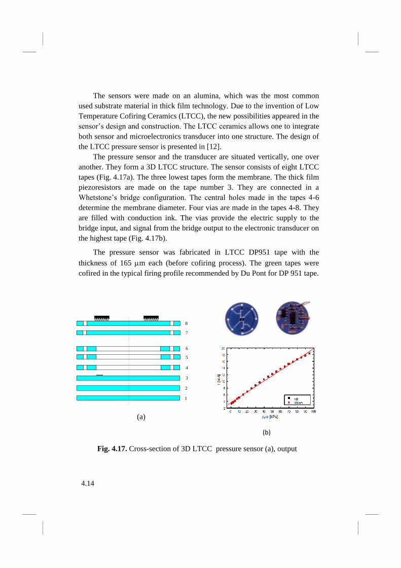
The pressure sensor and the transducer are situated vertically, one over
another. They form a 3D LTCC structure. The sensor consists of eight LTCC
tapes (Fig. 4.17a). The three lowest tapes form the membrane. The thick film
piezoresistors are made on the tape number 3. They are connected in a
Whetstone’s bridge configuration. The central holes made in the tapes 4-6
determine the membrane diameter. Four vias are made in the tapes 4-8. They
are filled with conduction ink. The vias provide the electric supply to the
bridge input, and signal from the bridge output to the electronic transducer on
the highest tape (Fig. 4.17b).
The pressure sensor was fabricated in LTCC DP951 tape with the
thickness of 165 m each (before cofiring process). The green tapes were
cofired in the typical firing profile recommended by Du Pont for DP 951 tape.
(a)
(b)
Fig. 4.17. Cross-section of 3D LTCC pressure sensor (a), output
8
7
6
5
4
3
2
1
4.14

4.15
characteristics of the pressure transducer (b) [12]
Another construction of the LTCC pressure sensor is presented in
Fig. 4.18. The principle of work is the same as described before
(piezoresistive effect). The sensor sensitivity depends on the diaphragm
thickness (Fig. 4.19).
Fig. 4.18. LTCC-based pressure sensor (finally assembled) [13]
Fig. 4.19. Sensor sensitivity (calculated vs. measured values) depending on the
diaphragm thickness [13]
4.15

4.16
The thick film pressure sensor can also work on the base of
piezoelectric effect or changes of /in capacitance. Such sensors were
presented by Belavic [14]. The cross-sections of the sensors are shown in
Fig. 4.20 and Fig. 4.21, respectively.
Fig. 4.20. Cross-section of the piezoelectric resonant pressure sensor
(schematic - not to scale) [14]
Fig. 4.21. A cross-section of a thick film capacitive pressure sensor (not to
scale). The construction is on the left and the working condition is
on the right [14]
4.16
4.17
4.4. Force sensors
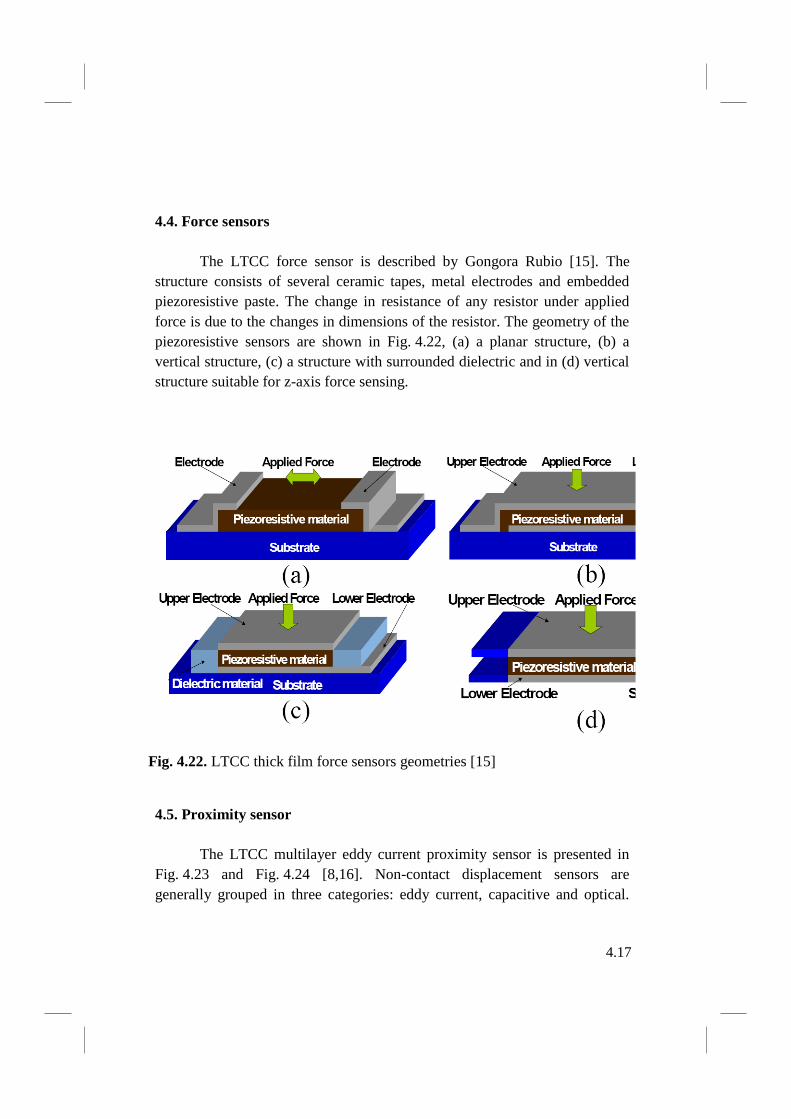
The LTCC force sensor is described by Gongora Rubio [15]. The
structure consists of several ceramic tapes, metal electrodes and embedded
piezoresistive paste. The change in resistance of any resistor under applied
force is due to the changes in dimensions of the resistor. The geometry of the
piezoresistive sensors are shown in Fig. 4.22, (a) a planar structure, (b) a
vertical structure, (c) a structure with surrounded dielectric and in (d) vertical
structure suitable for z-axis force sensing.
Fig. 4.22. LTCC thick film force sensors geometries [15]
4.5. Proximity sensor
The LTCC multilayer eddy current proximity sensor is presented in
Fig. 4.23 and Fig. 4.24 [8,16]. Non-contact displacement sensors are
generally grouped in three categories: eddy current, capacitive and optical.
4.17

4.18
Eddy current proximity sensors, in particular ceramic ones, could be used in
many industrial applications due to their ability to work in harsh
environments. The applications range are from metallic target positioning,
detection of holes, rivets or screws, precise measurement of automobile wheel
position in ABS braking systems. The eddy current proximity sensor has a
multilayer coil incorporated into a LC oscillator as shown in Fig. 4.24. When
this circuit is powered-up it creates a weak electromagnetic field near the coil.
If metallic targets are introduced in this field, eddy currents are induced in the
target changing the circuit output frequency by the modification of the coil
inductance.. The fabricated proximity sensor exhibits the following
properties: non-contact device, full scale of hundreds micrometers, could
work at high temperature and with various materials (different dielectric
constants) in the gap region. A multilayer square spiral coil of 1 cm x 1 cm
with special geometry was designed in order to reduce the quantity of
interconnection vias. A single layer was designed to make silver conductors
of 80 µm lines and 10 µm thickness with 80 µm space between the lines,
forming a 20-turn single layer coil. A five-layer proximity sensor coil was
fabricated using DuPont 951 LTCC ceramic system following a typical
process sequence, using interconnecting vias of 250 µm. 3D planar non-
contact proximity sensors with low internal capacitance allow to use higher
frequency in the associated oscillator. In addition it allows reduced
dimensions for better target tracking, 3 mm full-scale measurements,
operation at moderate temperature and it is fully compatible with all hybrid
electronics. The proximity sensor characteristics are shown in Fig. 4.25.
4.18
Fig. 4.23. Block diagram of a proximity sensor [8]

4.19
Fig. 4.24. Coil geometry and interconnection for a proximity sensor [8]
Fig. 4.25. A proximity sensor characteristics [16]
References
[1] J.W. Gardner, Microsensors, Wiley, New York, 1995.
[2] L. Michalski, K. Eckersdorf, J. Kucharski, Termometria przyrządy i
metody, Politechnika Łódzka, 1998.
4.19

4.20
[3] P. Markowski, A, Dziedzic, E. Prociów, Thick/thin film thermocouples
as Power Source for autonomous Microsystems - preliminary results,
Proc. Conf. IMAPS Poland Chapter, Wroclaw 2004.
[4] M. Prudenziati, Thick film sensors, Elsevier Science B. V., Amsterdam,
1994.
[5] J. Kita, Ph.D. Dissertation, Wroclaw University of Technology, 2003.
[6] http://www2.dupont.com/MCM/
[7] http://www.electroscience.com/
[8] M.R. Gongora-Rubio, P. Espinoza-Vallejos, L. Sola-Laguna, J.J.
Santiago-Aviles, Overview of low temperature co-fired ceramics tape
technology for meso-system technology (MsST), Sensors & Actuators
A89, 222-241 (2001).
[9] D. Güleryüz, W. Smetana, Mass Flow Sensor Realized in LTCC-
Technology, Proc. Conf. IMAPS Poland Chapter, Koszalin-Darłówko
2005, pp. 373-376.
[10] D. Jurków, L. Golonka, H. Roguszczak, LTCC gas flow detector, Proc.
16th
European Microelectronics and Packaging Conf., Oulu (Finland),
2007, pp. 204-207.
[11] A. Cattaneo, R. Dell’Acqua, G. Dell’Orto, L. Pirozzi, C. Canali, A
practical utilization of the piezoresistive effect in thick film resistors: a
low cost pressure sensor, Proc. IMS (ISHM-USA), 1980, pp. 221-228.
[12] L.J. Golonka, A. Dziedzic, H. Roguszczak, S. Tankiewicz, D. Terech,
Novel technological and constructional solutions of pressure sensors
made in LTCC technology, Optoelectronic and Electronic Sensors IV,
Jerzy Frączek, Editor, Proceedings of SPIE, 2000, vol. 4516, pp.10-14.
[13] U. Partsch, D. Arndt, H. Georgi, A new concept for LTCC based
pressure sensors, Proc. CICMT Conference, Denver 2007, pp. 367-372.
[14] D. Belavic et al., Benchmarking different types of thick-film pressure
sensors, Proc. CICMT Conference, Denver 2007, pp. 278-285.
[15] M.R. Gongora-Rubio et al, LTCC post load cell, Proc. CICMT
Conference, Denver 2006.
[16] M.R. Gongora-Rubio, L.M. Sola-Laguna, M. Smith, J.J. Santiago
Aviles, LTCC technology multilayer eddy current proximity sensor for
harsh environments, Proc. of the 32nd Int. Symp. on Microelectronics,
IMAPS'99, 1999, Chicago, pp. 676-681.
4.20

5.1
Chapter 5
LTCC and thick film chemical sensors
5.1. Humidity sensors
There are many methods of measuring humidity. Some of them are
presented in Table 5.1.
Table 5.1.
Methods of humidity measurement
Principle Operating mechanism
Capacitance dielectric constant of material varies with absorbed
water
Dew point temperature corresponding to condensation-evaporation
equilibrium at a cooled surface varies with H2O
Resisitance conductivity depends on H2O absorbed
Piezoelectric hygroscopic coating changes crystal frequency
Gravimetric a volume of moist air is exposed to a drying agent,
subsequently weighted
Hygroscopic length of fibre varies with H2O
Infrared absorption from 1.5 to 1.93 μm
. . .
Two groups of materials are commercially used as resistance or
capacitance humidity sensors: organic polymers and ceramics. Polymer
sensors exhibit the disadvantages of hysteresis, slow response time, long-term
drift and degradation upon exposure to some solvents. Moreover, they cannot
operate at high temperature and humidity. Ceramic sensors have advantages
over the polymer sensors in terms of better thermal stability and resistance to
chemicals. However, ceramic sensors need periodic thermal regeneration to
recover their humidity-sensitive properties. Thick film technology enables
reproducible production of ceramic sensors with a defined microstructure,
determined porosity and proper structure of grains and grain boundaries.
These factors are vital for the development of humidity sensors with good
parameters. Moreover, both the humidity sensor and the heater used for
5.1

5.2
periodic regeneration can be made on a single substrate in the same
technological process. Integration of the sensor and the electronic
conditioning system is also possible. Most thick film humidity sensors work
on the principle of impedance variation. The change in impedance, resistance
or capacitance measured at a constant frequency, with relative humidity
changes is widely used in practice. Thick film humidity sensor characteristics
depend on the bulk and surface properties of the ceramic material. The
properties are determined by the pore size distribution, average particle size
and additives [1].
The humidity sensor requirements:
- high sensitivity in a wide humidity range,
- short response time,
- reproducibility (no hysteresis),
- long life time,
- resistance to impurity,
- no influence of temperature,
- simple construction,
- low cost.
Disadvantages of the humidity sensors:
- long-term drift,
- limited operating temperature range,
- slow response time and hysteresis.
There are many fields of humidity sensors applications:
- industrial processes,
- human health and comfort,
- home appliances,
- electronic equipment,
- medical equipment,
- agriculture,
5.2

5.3
The mechanisms of water adsorption are very important in case of ceramic
sensors. Water can be adsorbed in three various ways. There are:
- chemical adsorption,
- physical adsorption,
- free water (macropores).
The strongest adsorption force is in the case of the chemical
adsorption, where the first monolayer of water is formed on the material
surface. The successive water layers are adsorbed by physical forces. The
weakest connection of water to the material occurs in macropores where free
water is adsorbed. Very important for proper designing of ceramic humidity
sensors is the knowledge of the adsorption – sorption curves. The dependence
of such curves upon temperature and the kind of material is shown in Fig. 5.1.
Fig. 5.1. H2O adsorption – sorption curves (T - temperature, φ - relative
humidity, m - mass of adsorbed water)
5.3

5.4
There are many parameters describing the level of humidity in the air.
The most popular one is the relative humidity, marked by RH, RH or φ . The
definition of the relative humidity is shown in Fig. 5.2.
Fig. 5.2. Curve ps versus T with marked parameters used for definition of the
relative humidity in air
Ceramic humidity sensors
Humidity sensing principle of porous oxide semiconductors
(MgCr2O4-TiO2
, MnWO4, etc.)
is based on electrical conductivity
measurements. Bulk resistivity is measured as impedance. The sensitivity of
"porous” oxide semiconductors is satisfactory. Dopants added to the mixture
play a role of catalyst. They promote the dissociation of adsorbed water into
hydrogen and hydroxyl ions. The hydroxyl ions reduce the bulk resistivity.
Electrical properties of the ceramic humidity sensor depend on:
- surface properties (hydrophobic, hydrophilic),
- microstructure (pore sizes distribution),
- electrical properties of the material.
The ceramic sensors exhibit some disadvantages. Humidity sensing
mechanism is based on the adsorption of water vapour and therefore there is
a degradation by surface contamination.
5.4

5.5
The structure of thick film ceramic humidity sensor is presented in
Fig. 5.3. Schematic illustration of water adsorption at various level of relative
humidity in the air is shown in Fig. 5.4.
Fig. 5.3. The structure of thick film ceramic humidity sensor [2]
Fig. 5.4. Schematic illustration of water adsorption [2]
5.5

5.6
The RH dependence of resistance log R = f(RH) for the ZnCr2O4–
TiO2 thick film sensor is presented in Fig. 5.5 [1]. The characteristics were
measured at the optimal working frequency (maximum of sensitivity). The
changes of resistance with humidity encompass four orders of magnitude.
The characteristics can be approximated by a straight line. The relationship
between the logarithm of resistance and relative humidity follows an almost
perfect straight line.
The response time to the variation of RH is influenced by the
microstructure, which depends on the micropores formation and the sintering
conditions due to the thermal treatment. A fast response time is obtained in
the case of large pores. The easy adsorption and desorption of water
molecules are the dominating processes [1].
Fig. 5.5. The RH dependence of resistance for the ZnCr2O4–TiO2 sensor [1]
5.6

5.7
5.2. Gas sensors
Semiconductor gas sensors
Two types of thick film gas sensors are mainly used: semiconductor
and electrochemical. The semiconductor ones are based mostly on Sn and Zn
oxides as gas sensitive material. The resistance of the sensor depends on the
gas concentration. Poor sensitivity is the main disadvantage of such sensors.
To overcome this problem the gas sensor array is made on one substrate. The
sensors in the array are made from various gas sensitive materials and work at
different temperatures. The response of each sensor to various gases is
different. The selectivity can be improved by collecting the data from all
sensors. The array of thick film sensors made from gas sensitive
semiconductors ZnO, SnO2 and WO3 with various dopants is presented in
Fig. 5.6 [3]. The sensitivity of these sensor materials to various gases is
shown in Fig. 5.7. The height of the energetic barrier between semiconductor
oxide grains depends on the gas concentration (Fig. 5.8). It explains the
dependence of sensor resistance versus gas concentration. Thick film gas
sensor structure is shown in Fig. 5.9.
Fig. 5.6. Array of thick film gas sensors [3].
5.7

5.8
G
as
se
ns
itiv
ity
(G
/Go)
Gas concentration [ppm]
Fig. 5.7. Gas sensitivity versus different gases concentration for the sensors
made from various gas sensitive thick film semiconductor oxides
shown in Fig. 5.6 [3]
(a)
(b)
Fig. 5.8. The model of inter-grain potential barrier: in absence of gases (a), in
presence of reducing gases (b) [4]
5.8

5.9
(a)
(b) (c)
Fig. 5.9. Thick film gas sensor: schematic draw (a), thick film substrate with
gas sensitive material (b), sensor with a metal cover (c) [5]
Fig. 5.10. Design of LTCC multilayer gas sensor [6]
The design of thick film gas sensor made on LTCC multilayer is presented in
Fig. 5.10. Characteristics of the LTCC gas sensor embedded heater and the
sensor response to CH4 and CO are presented in Fig. 5.11 and 5.12,
respectively.
5.9

5.10
Fig. 5.11. Characteristics of LTCC gas sensor heater [7]
Fig. 5.12. LTCC gas sensor response [7]
Electrochemical gas sensors
Thick film and LTCC electrochemical gas sensors are made from
solid state electrolyte. There is only ion conductivity in such electrolytes. The
sensors work at high temperature so as to ensure appropriate level of
electrical conductivity. There are two modes of the sensors work:
potentiometric (the electromotoric force generated on the sensor electrodes
depends on the difference in the gas concentration on the both sides of the
thick film electrolyte - Fig. 5.13) and amperometric (electrical current
depends on the gas concentration - Fig. 5.14).
5.10

5.11
Nernst equation
Fig. 5.13. Potentiometric gas sensor - schematic draw and basic characteristics
Fig. 5.14. Electrochemical amperometric O2 sensor [5]
There are many advantages of electrochemical gas sensors:
- simple measurement of the generated voltage,
- gas partial pressure directly converted to electrical signal,
- generated voltage does not depend upon the sensor dimension,
- good selectivity,
- generated voltage depends logarithmically upon gas,
5.11

5.12
concentration measurements in very wide range,
- calibration not required,
- very good mechanical properties (vibration, acceleration resistant),
- chemical inertness,
- long life time,
- stability in wide temperature range,
- low power,
- easy management,
- low cost.
Disadvantages of the electrochemical gas sensors:
- long response time,
- low accuracy in measurements of small concentration
changes (logarithmic scale),
References
[1] L. Golonka, B.W. Licznerski, K. Nitsch, H. Teterycz, Thick-film
humidity sensors, Meas. Sci. Technol. 8, 1997, pp. 92–98.
[2] L. Golonka, B.W. Licznerski, K. Nitsch, H. Teterycz, Thick film
humidity sensors based on different materials, Int. Symposium on
Microelectronics ISHM, Los Angeles (USA), 1995, Proc. pp. 107-112.
[3] M. Kaneyasu, M. Ikegami, A. Arima, H. Iwanaga, S., Smell
Identification using a thick-film hybrid gas sensor, IEEE Transactions on
Components, Hybrids, and Manufacturing Technology vol. 10 (2), 1987,
pp. 267-273.
[4] Figaro gas sensors - data sheet.
[5] www.ett.bme.hu
[6] H. Teterycz, J. Kita, R. Bauer, L. Golonka, B.W. Licznerski, K. Nitsch,
K. Wiśniewski, New design of SnO2 gas sensor on Low Temperature
Cofiring Ceramics, Sensors and Actuators B, vol.47/1-3, 1998, pp. 100-
103.
[7] H. Teterycz, J. Kita, R. Bauer, L. Golonka, B.W. Licznerski, K. Nitsch, K.
Wiśniewski, New design of SnO2 gas sensor on Low Temperature
Cofiring Ceramics, Eurosensors Conf., Warsaw, 1997.
5.12
6.1
Chapter 6
Foundation of microfluidics
6.1. Introduction
Microfluidics is the term that is used to describe flow in miniature devices
having characteristic dimensions ranging from single millimetres to hundreds
of nanometers. The microfluidic devices thanks to their very small size are
capable of handling volume of fluid (gas or liquid) in range of nano- and
microliters (10-9
– 10-6
l) [1,2]. In the last two decades there has been an
explosion of scientific papers in this area. There are several reasons for this
interest. One of the reasons is rapid development of the microelectronic
technologies (e.g. silicon micromachining). The progress which has been
made in nano- and microtechnology enables fabrication of various precise
and complex spatial structures (channels, cavities, chambers, cantilevers,
membranes etc.) with characteristic dimensions up to hundreds of
nanometers. Another aspect is the number of possible areas of microfluidic
system applications: analytical chemistry, medical diagnosis, DNA
sequencing, cell separation, microbiological analysis, high-throughput
synthesis, environmental monitoring and others. Analytical procedures which
are applied in modern chemistry, biology and medicine consists of several
steps: sample collection, carrying out an appropriate (bio)chemical reaction,
separation of reaction products and detection of the analyte. Classical
laboratory equipment is characterized by relatively long time of detection,
lack or poor process control, considerable reagents consumption and large
amount of wastes. All these disadvantages can be eliminated by use of the
microfluidic devices. Thanks to the fact that these microsystems work with
liquid or gas samples in the micro- or nanoliter scale, they are characterized
by short response time, high sensitivity and good selectivity, Moreover,
6.1

6.2
microfluidic system produces less wastes and is much safer (especially when
it works with a toxic, poisonous or explosive substance) in comparison with
classical laboratory equipment used in analytical chemistry, biology or
medicine.
6.2. Basic terms and equations of fluid dynamics
Reynolds number
According to chemical and process engineering there are generally two
patterns of fluid flow:
(1) Laminar flow
(2) Turbulent flow
For laminar flow, the forces connected with fluid viscosity dominate. As a
result of this, the laminar flow is a calm flow of the fluid that moves orderly
along the streamlines. Turbulent flow, on the other hand, is much more
violent. In this case, inertia forces exceed viscous effects. As a consequence
the fluid particles move chaotically in all direction without any traceable
pattern. The transition from laminar to turbulent flow pattern is determined by
the Reynolds number:
(6.1)
where is a fluid density (kg/m3), U is a mean fluid velocity (m/s), L is a
characteristic dimension (m) and is a fluid viscosity (Pa·s). The transition
from laminar to turbulent flow occurs for Re > 2300. In this case, the inertia
forces dominate over the viscous effects and as a result fluid recirculations
and vortices are generated. However, due to very small dimensions, of almost
all microfluidic systems, the fluid flow is nearly always in the laminar flow
regime. A comparison between a laminar and turbulent flow of a fluid in a
circular tube is given in Table 6.1.
6.2

6.3
In practice, a conduit geometry can significantly influence the value of the
Reynolds number at which the transition from laminar to turbulent flow
occurs. Therefore, the parameter L given in equation (6.1) is very often
replaced by a hydraulic diameter Dh. It is a commonly used term when
handling the fluid flow in non-circular channels. The hydraulic diameter is
defined as:
(6.2)
where A is a cross sectional area of the conduit (m2) and O is the “wet
perimeter”. It is the conduit’s perimeter that is in contact with the fluid. It can
6.3

6.4
be noticed that hydraulic diameter from the equation (6.2) for a circular tube
stands for its diameter d:
(6.3)
However, in case of microfluidic structures the channels are not circular. The
hydraulic diameter for a rectangular conduit with the width w and height h is
equal to:
(6.4)
for w = h (square channel):
(6.5)
The second parameter from equation (6.1) which should be defined more
precisely is the mean fluid velocity U. According to chemical engineering it
can be defined as:
(6.6)
where Q is a fluid volumetric flow (m3/s).
The continuity equation
During the flow of a fluid through a conduit, the mass flow is constant in
every place of the channel. The continuity equation of fluid flow is used to
determine the volumetric flow rates. Fig. 6.1 illustrates a control volume of
the fluid enclosed between two surfaces A1 and A2 which are separated by an
6.4

6.5
infinitesimally small distance dl. The mean velocity and density of the fluid at
the surface A2 are equal to:
(6.7)
(6.8)
(6.9)
Fig. 6.1. Continuous fluid flow in a conduit.
The mass flow rate at the inlet and outlet is equal to:
(6.10)
(6.11)
By the law of mass conservation, we should obtain the following relation:
(6.12)
6.5

6.6
therefore, the rate of the mass flow in the steady-state flow condition with
, or:
(6.13)
For incompressible fluids (e.g. liquids) equation (6.13) can be used to
determine the volumetric flow rate:
(6.14)
The fluidic dynamic continuity equation is analogous to Kirchoff’s Current
law known from electronic circuits. The rate at which mass enters is equal to
the rate at which it leaves the system (Fig. 6.2).
Fig. 6.2. Illustration of the fluidic continuity equation.
Navier-Stokes equation
Mathematical description of fluid flow is based on momentum conservation
law which is represented by the Navier-Stokes equation. Derivation of the
equation is beyond the scope of this book. It can be find in fluid dynamics
6.6

6.7
books [e.g. 3,4]. For a general case the equation can be presented in the
following form:
(6.15)
It is a partial differential equation in which u = (u, v, w) is the fluid velocity
vector with (m/s) unit, p is a pressure (Pa) and F is an external driving force
(N).
The presented Navier-Stokes equations are partial differential equations
which have analytical solutions only for a few very simple cases. Therefore,
more sophisticated cases have to be solved using CFD (Computational Fluid
Dynamic) methods. Although equation (6.15) describes the incompressible
flow, it is valid for the flows with spatially varying density ρ = ρ(x, y, z) and
viscosity µ = µ(x, y, z) as well. For the flows with constant density and
viscosity (e.g. liquids), the Navier-Stokes equation can be simplified to:
(6.16)
In case of microfluidic systems, it is common that the Reynolds number is
very low and the fluid flow can be approximated as a creeping flow (Stokes
flow). In a consequence, the convection term in equation (6.16) can be
neglected and the Navier-Stokes equation simplifies to:
(6.17)
The Stokes flow can be regarded as a quasi-steady flow, therefore, the time
derivative term from equation (6.17) can be also neglected and the fluid flow
in a microscale can be described by equation:
6.7

6.8
(6.18)
Pressure drop
During a fluid flow through a conduit losses of energy occur. This lost energy
is returned to the surroundings in form of heat. Fluid energy losses are caused
by a hydraulic resistance which can be indentified by pressure drop along the
fluidic conduit. The pressure drop occurs as a result of changes of the fluidic
channel configuration (broadening or contraction of the cross-sectional area)
and due to friction between the fluid and contacting conduit’s walls (viscous
losses). The pressure drop caused by broadening of the channel’s cross-
sectional area (Fig. 6.3) can be described by the equation:
(6.19)
(6.20)
Fig. 6.3. Broadening of the conduit’s cross-sectional area.
where P is a pressure drop (Pa) and is a coefficient of local resistance.
The pressure drop takes place during contracting of the conduit’s cross-
sectional area, as well (Fig. 6.4). Inertia of the fluid stream causes an increase
of fluid velocity and contraction of the flow area. However, the increase of
6.8
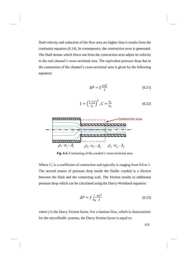
6.9
fluid velocity and reduction of the flow area are higher than it results from the
continuity equation (6.14). In consequence, the contraction area is generated.
The fluid stream which flows out from the contraction area adjust its velocity
to the real channel’s cross-sectional area. The equivalent pressure drop due to
the contraction of the channel’s cross-sectional area is given by the following
equation:
(6.21)
(6.22)
Fig. 6.4. Contracting of the conduit’s cross-sectional area.
Where C1 is a coefficient of contraction and typically is ranging from 0.6 to 1.
The second reason of pressure drop inside the fluidic conduit is a friction
between the fluid and the contacting wall. The friction results in additional
pressure drop which can be calculated using the Darcy-Weisbach equation:
(6.23)
where f is the Darcy friction factor. For a laminar flow, which is characteristic
for the microfluidic systems, the Darcy friction factor is equal to:
6.9

6.10
(6.24)
where Re is the Reynolds number and C2 is a friction coefficient which
depends on the conduit’s geometry. Exemplary values of the friction
coefficient are presented in table 6.2.
Table 6.2. Friction coefficient for various configurations of the fluidic channel.
Configuration Dh D
Circular d 64
Square w=h 57
Rectangular 2wh/(w+h) 96
Scaling laws in microfluidics
When the characteristic dimensions of the system decrease from macroscopic
to the microscopic scale, some effects that are negligible at macroscale
become significant at microscale, and vice versa. For example the effects of
gravity become negligible in comparison with the adhesive and friction
effects [5]. Surface tension and viscous forces of the fluid have a significant
impact on a fluid flow in microscale. They can drastically and rapidly damp
any motion. At high velocities, the hydrodynamics is unstable, and the
turbulent flow occurs. According to the description given in the previous
section of this book, the transition from laminar to turbulent flow takes place
when Re > 2300. One phenomenon which can be deduced from equation (6.1)
is that the Reynolds number is directly proportional to the second power of
the conduit characteristic dimension:
(6.25)
6.10

6.11
This means that the turbulence disappears in the microsystems in which fluid
flows.
Similar observation can be made for the pressure drop in the fluid over the
channel length. The relation between the pressure drop and characteristic
dimension of the conduit can be derived from the Darcy-Weisbach formula
(6.23) and equation (6.1) and (6.24) as:
(6.26)
One interesting phenomenon can be concluded from equation (6.26). For a
circular tube the pressure drop is inversely proportional to the fourth power of
the tube radius r:
(6.27)
(6.28)
A similar calculations can be made for other configurations of the fluidic
channel:
for a square channel:
(6.29)
for a rectangular channel:
(6.30)
The conclusion which comes from equations (6.28), (6.29) and (6.30) is that
the 16 times higher pumping power would be required to pump the same
6.11

6.12
amount of volumetric flow of fluid with the conduit dimensions reduced by
half.
Another important aspect which has to be taken into account is the influence
of surface tension. The surface tension in liquids relates to the cohesion forces
of the molecules. As can be seen in Fig. 6.5, for the molecules in the liquid
there is a balance of the cohesive forces. However, the molecules which are
closer to the liquid-gas or liquid-solid interface are not bonded in the same
way. When the cohesive forces between the molecules located inside the
liquid are larger than interaction with gas/solid molecules, the contact area
becomes concave upward. The surface tension Fs in a liquid can be expressed
as:
(6.31)
where S is a wet perimeter (m) and is a coefficient of surface tension (N/m).
Fig. 6.5. Superficial tension forces at the interface between a liquid and air.
The influence of surface tension becomes significant in the case of fluid flow
in microchannels, as an additional pressure has to be overcome to move the
liquid [6]. The relation between the surface tension and pressure is given by
the Laplace equation:
6.12

6.13
(6.32)
where C is the curvature of the fluid surface. The curvature depends on
geometry of the microconduit and can be defined as:
for a circular tubes:
(6.33)
for a non-circular tubes:
(6.34)
where r is the curvature radius for the fluid in a circular tube and r1 and r2 are
the curvatures of a non-circular conduit.
One can notice that reducing of the channel dimensions leads to an increase in
pressure drop due to fluid surface tension. For example, the total pressure
change in a free-standing liquid inside a circular conduit with a diameter d =
2r, as shown in Fig. 6.6, can be estimated as a sum of the pressure changes in
the liquid cylinder and liquid sphere [7]:
(6.35)
Fig. 6.6. Fluid volume in a circular tube.
6.13

6.14
For a liquid cylinder, as presented in Fig. 6.7, the pressure change due to
surface tension can be calculated by dividing the surface tension Fs by the
lateral area of the cylinder (2rL).
Fig. 6.7. Pressure change due to surface tension across the liquid cylinder [7].
According to equation (6.31) surface tension is equal to wet perimeter (2L)
times the coefficient of surface tension (Therefore, the pressure change in
the liquid cylinder due to the surface tension is equal to:
(6.36)
The pressure change due to surface tension for a liquid sphere, as presented in
Fig. 6.8, can be calculated using analogous procedure, from which we have:
(6.37)
Therefore, according to equations (6.35), (6.36) and (6.37) the total pressure
change in a free-standing liquid inside a circular conduit is equal to:
6.14

6.15
(6.38)
Fig. 6.8. Pressure change due to surface tension across the liquid sphere [7].
The coefficient of surface tension depends on the contact angle between the
liquid and the solid. For a hydrophobic materials the contact angle is high
while for hydrophilic materials are characterized by good wettability (low
contact angle). Therefore, the use of hydrophobic material increases the
pressure which is required to move the fluid inside the microchannel. As can
be seen in Fig. 6.9 the pressure required to move the liquid (P1) is higher
when the liquid–air interface reaches the region of increased hydrophobicity
(P2) [6].
Fig. 6.9. Influence of the hydrophobic material upon pressure drop [6].
6.15

6.16
References
[1] Ottino JM, Wiggins S, Introduction: mixing in microfluidics, Royal
Society of LondonTransactions Series A, 362 (2004) 923-935.
[2] Gravessen P, Branebjerg J, Jansen OS, Microfluidics – a review, Journal
of Micromechanics and Microengineering, 3 (1993) 168-182.
[3] Shaughnessy EJ, Katz IM, Schaffer JP, Introduction to fluid mechanics,
Oxford University Press, 2005.
[4] Batchelor GK. Introduction to Fluid Dynamics, Cambridge University
Press, 1967.
[5] Wautelet M, Scaling laws in the macro-, micro- and nanoworlds.
European Journal of Physics, 22 (2001) 601-611.
[6] Li D (ed.), Encyclopedia of microfluidics and nanofluidics, Springer,
2008.
[7] Hsu TR, MEMS and microsystems design and manufacture, McGraw
Hill, 2002.
6.16

7.1
Chapter 7
Technology of the LTCC-based microfluidic systems
7.1. Introduction
The chapter presents the basic method of three-dimensional (3D) structuration
of the LTCC material for the applications in microfluidics. The low
temperature co-fired ceramics has been used in microelectronics since the end
of the 1980’s. It has been applied to the fabrication of hybrid electronic
circuits and ceramic multilayer structures. A typical LTCC module consists
of several dielectric (alumina filled glasses or glass-ceramic) tapes,
connecting vias, surface and buried thick films (conductors and passives).
The conductive lines and passive components (resistors, capacitors and
inductors) are deposited using standard printing technologies (screen-printing,
ink-jet printing). After the deposition of thick films, all LTCC tapes are
stacked together in proper order and bonded during/in a lamination process.
Finally, the multilayer laminate is co-fired at the temperature of 850-900oC.
Additional active and passive components can be added on the top or the
bottom surface of the fired structure using wire-bonding, flip-chip or surface
mounting technique (SMT). Nowadays, the LTCC technology is mainly used
for automotive and telecommunication applications. However, there has been
a growing interest in the developing of fluidic structures using LTCC
technology in recent years. The ceramic-glass material is increasingly used
for microfluidic application thanks to its outstanding physical and chemical
properties. The sintered LTCC is chemically inactive and resistant to water,
saline solutions, organic substances, solvents and some of acids and bases.
Low temperature co-fired ceramics is characterized by a good thermal
conductivity, high temperature and pressure stability. Moreover the complex
and precise three-dimensional (3D) structures can be made inside the LTCC
7.1

7.2
substrate using various micromachining techniques. Quite recently,
microfluidic systems have been manufactured mainly using silicon
technology. However, according to the newest trends, cheaper technologies
and materials are applied. The modern microfluidic devices are fabricated
using relatively cheap polymeric, PCB (printed circuit board) and ceramic
technologies. The advantages of the LTCC technique, in comparison with the
silicon one, are lower price and shorter time of the new microsystem
development. Moreover, the fabrication process of the LTCC microfluidic
systems is much simpler. In comparison with PCB technology, the
advantages of LTCC technology are following: chemical inactivity, chemical
resistance, biocompatibility and high temperature stability. Moreover, the
LTCC tapes can be easily cut into desired form in the way to accomplish both
mechanical and electrical function in a single ceramic microsystem. The
possibility of integration of fluidic channels, active and passive electronic
components, sensors, actuators, MEMS (Micro Electro-Mechanical Systems)
devices and package into a one module is the main benefit of the LTCC over
the polymer technology. Moreover, the low temperature co-fired ceramics can
be bonded with other materials using anodic bonding (LTCC-silicon),
microwave plasma (LTCC-polymer) or low temperature glass (LTCC-glass,
LTCC-ceramics). Due to all above-mentioned advantages, the LTCC has
found practical application in microfluidics as flow sensors, micromixers,
micropumps, microvalves, microreactors, microanalyzers, electrochemical
sensors, cell sorting and DNA sequencing devices.
In this chapter, the challenges and issues connected with the fabrication
process of precise microfluidic components in a multilayer LTCC substrate
are discussed. Subsequently, an overview of the techniques for
micromachining the of 3D structures in the green (unfired) and fired ceramic
material is provided. Low and higher pressure lamination methods, laser
7.2
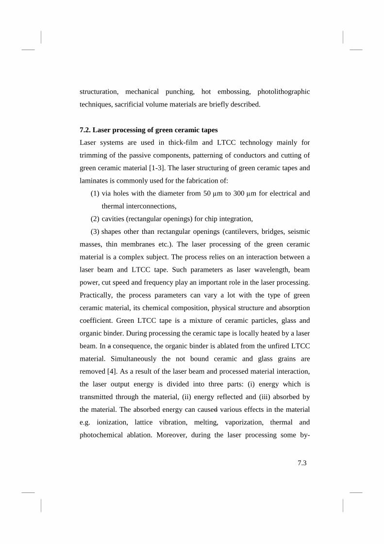
7.3
structuration, mechanical punching, hot embossing, photolithographic
techniques, sacrificial volume materials are briefly described.
7.2. Laser processing of green ceramic tapes
Laser systems are used in thick-film and LTCC technology mainly for
trimming of the passive components, patterning of conductors and cutting of
green ceramic material [1-3]. The laser structuring of green ceramic tapes and
laminates is commonly used for the fabrication of:
(1) via holes with the diameter from 50 µm to 300 µm for electrical and
thermal interconnections,
(2) cavities (rectangular openings) for chip integration,
(3) shapes other than rectangular openings (cantilevers, bridges, seismic
masses, thin membranes etc.). The laser processing of the green ceramic
material is a complex subject. The process relies on an interaction between a
laser beam and LTCC tape. Such parameters as laser wavelength, beam
power, cut speed and frequency play an important role in the laser processing.
Practically, the process parameters can vary a lot with the type of green
ceramic material, its chemical composition, physical structure and absorption
coefficient. Green LTCC tape is a mixture of ceramic particles, glass and
organic binder. During processing the ceramic tape is locally heated by a laser
beam. In a consequence, the organic binder is ablated from the unfired LTCC
material. Simultaneously the not bound ceramic and glass grains are
removed [4]. As a result of the laser beam and processed material interaction,
the laser output energy is divided into three parts: (i) energy which is
transmitted through the material, (ii) energy reflected and (iii) absorbed by
the material. The absorbed energy can caused various effects in the material
e.g. ionization, lattice vibration, melting, vaporization, thermal and
photochemical ablation. Moreover, during the laser processing some by-
7.3

7.4
products (vapour, debris) are generated which can influence the process. The
laser ablation of a material is dependent on absorption and thus (dependent)
on the wavelength of the laser radiation. Common wavelengths of industrial
lasers are 10600 nm (IR), 1064 nm (NIR), 532 nm (VIS, green), 355 nm
(UV). The absorption of laser radiation is furthermore dependent on other
factors e.g. temperature, laser pulse width.
Generally laser systems can operate in two modes: continuous wave (CW)
and pulsed. The modes of operation describe the laser energy distribution in
time (Fig. 7.1). For the CW mode the energy of laser beam is relatively low
while for the pulse mode energy of the beam depends on repetition rate, pulse
width (duration) and pulse power. All these parameters have a very strong
influence on the laser ablation of the green LTCC tape.
Fig. 7.1. The energy distribution in time for different modes of operation [5].
There are three basic laser structuring techniques: laser cutting, engraving
(ablation) and drilling. In the laser cutting method a single or multiple pass
7.4

7.5
approach can be used. The single pass approach consists in a single cutting
cycle at high energy. The laser beam energy should be sufficient to cut the
green ceramic tape through. In opposite to the single pass approach the
multiple pass approach consists in repeated cutting cycles at lower energy
(higher laser beam speed). Each approach leads to different results. On a one
hand the single cutting cycle is a bit faster. On the other hand the multi-pass
approach leads to thinner cutting kerfs and better cutting quality. However,
the heat accumulated during the multiple cutting cycles can caused melting of
the glass phase in the LTCC tape. This phenomenon is especially visible for
thicker tapes. Exemplary kerfs made with the use of a single and a multiple
pass approach are presented in Fig. 7.2.
Fig. 7.2. LTCC kerfs obtained by (a) single cutting cycle (1 x 100 mm/s) and
(b) multiple cutting cycles (4 x 500 mm/s) [5].
The laser engraving is used for the fabrication of channels, cavities or other
structures within a single ceramic tape or a laminate. Energy of the laser
beam is adjusted to ablate some of tape material but not to cut it through. The
ablation depth depends on the laser energy. Therefore, variations of laser
beam scanning speed which results in different energy density absorbed by
the engraved material can caused not uniform depth profile of the final
7.5

7.6
structure. Exemplary channels made in green LTCC tape using the laser
engraving technique is presented in Fig. 7.3.
Fig. 7.3. Fluidic channel made in green LTCC tape by laser engraving [5].
The laser drilling is mainly used to fabricate via holes in green ceramic tape
for electric and thermal interconnections. The holes can by drilled using two
dimensional (trepanning) or three dimensional (helical trepanning) laser beam
movement (Fig. 7.4).
Fig. 7.4. Techniques of vias drilling using laser system.
The laser energy vaporizes the material layer by layer and ultimately creates a
through hole. The shape of the drilled hole is defined by the profile of the
laser beam. Therefore, the percussion drilled holes are somewhat tapered
7.6

7.7
(Fig. 7.5). As can be seen in Fig. 7.6 the tapering phenomenon increases with
the tape thickness [6].
Fig. 7.5. Tapered via holes drilled in a green LTCC tape using CO2 laser [5].
7.3. Mechanical machining of green ceramic tapes
The mechanical machining methods are used in order to obtain cavities,
channels (milling) or vias for electrical and thermal connection (punching)
between ceramic layers. The principles of mechanical milling and punching
are presented in Fig.s 7.7a and 7.7b, respectively.
Fig. 7.6. Difference in dimensions of laser-drilled vias [6].
7.7

7.8
Both mechanical patterning techniques are similar to laser machining. The
only difference between mechanical and laser machining is the of way
removing the unfired ceramic material. In the case of mechanical
milling/punching a piece of LTCC tape is removed due to mechanical
interaction between a milling/punching tool and green ceramic material. In
the case of mechanical milling it is possible to achieve complex geometries
with feature size of 100
a) b)
Fig. 7.7. Principles of mechanical milling (a) and punching (b) [7,8].
The quality and size of the final milled feature strongly depends on the
applied tool. Mechanical punching is usually carried out with a tool with
desired size and a die with an opening typically 12.5 mm larger in diameter
than the punch. Exemplary punching tool is presented in Fig. 7.8. An
automated punching machine can make from 5 to 500 holes per second,
depending on the complexity of the machine. The quality of vias produced by
mechanical punching depends on the proper alignment between the punch
and the die. If these two components are not well aligned then the via quality
decreases and the punching die is likely to be damaged. The advantage of the
mechanically punched vias in comparison with the laser drilled ones, is the
7.8

7.9
lack of the tapering phenomenon. The variation of the via diameter on the
punch and back side of the tape is presented in Fig. 7.9.
Fig. 7.8. Punching tool [8].
Fig. 7.9. Difference in dimensions of mechanically punched vias [6].
7.4. Hot embossing
The hot embossing is an alternative method for fluidic structures fabrication
in unfired ceramic substrate. Originally this method was applied to form
complex spatial structures in polymeric materials. In this technique the
7.9

7.10
pattern which consists of various geometries is transferred to the surface of
the green ceramic laminate. A flow-chart of the LTCC module three-
dimensional structuration using hot embossing is presented in Fig. 7.10.
Fig. 7.10. Three-dimensional structuration of LTCC substrate using hot embossing.
In the first step, few ceramic sheets are laminated using an isostatic or
uniaxial press in order to form a ceramic substrate. Then the LTCC laminate
is put on a heated traverse. The ceramic module and embossing die are heated
above glass transition temperature of the organic binder (typically > 70oC). In
the next step, the embossing die is driven down, impressing the pattern into
ceramic laminate. Hot embossing dies can be made of various materials such
as: polymers (PMMA), rubber, nickel, brass. The pattern is manufactured
using lithography, electroplating, LIGA (ger. Lithographie, Galvanoformung,
Abformung) technology, ultra-precision milling or laser ablation techniques
[9, 10]. Exemplary embossing dies are presented in Fig. 7.11.
7.10

7.11
Fig. 7.11. Embossing die made of brass [9].
The crucial parameters of an embossing process are: temperature, pressure,
time and material of the mould pattern. The depth of the impressed shape can
be increased by rising pressure and temperature of the process. However, too
high embossing temperature can cause sticking of the ”green” ceramic
material to the die, whereas too low temperature may result in cracking.
Moreover, high embossing pressure may induce cracks and fractures in the
ceramic substrate. Therefore, embossing parameters feed rate, pressure,
maximum temperature, and dwell time have to be optimized depending on the
properties of the specific LTCC tape [10]. A green ceramic laminate with a
structured surface with embossing die is presented in Fig. 7.12. Buried fluidic
structures can be fabricated using hot embossing method, as well. However,
uniaxial or isostatic lamination cannot be applied to bond structured laminate
and ceramic cover tape. Therefore, a low pressure lamination method has to
be used. The LTCC substrate with embossed structures can be joined with
ceramic cover tape using special adhesive layer (Fig. 7.13). The ceramic
laminate is covered by a mixture of polypropylene-glycol (PPG) and ethanol.
After that, the embossed laminate and the covering LTCC tape are stacked
together and pressed with a steel roller, followed by a storage for 24 h at a/
the temperature of 80oC. The applied solvent dissolves the surface of the
7.11
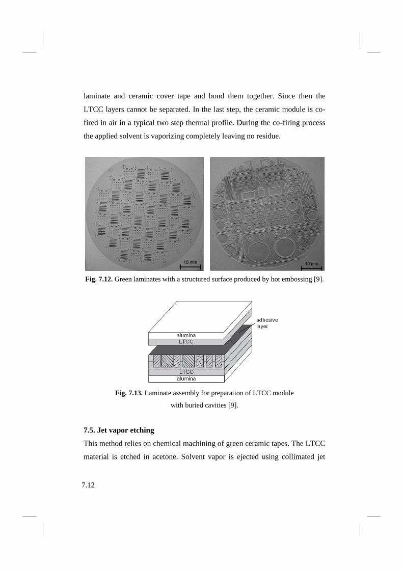
7.12
laminate and ceramic cover tape and bond them together. Since then the
LTCC layers cannot be separated. In the last step, the ceramic module is co-
fired in air in a typical two step thermal profile. During the co-firing process
the applied solvent is vaporizing completely leaving no residue.
Fig. 7.12. Green laminates with a structured surface produced by hot embossing [9].
Fig. 7.13. Laminate assembly for preparation of LTCC module
with buried cavities [9].
7.5. Jet vapor etching
This method relies on chemical machining of green ceramic tapes. The LTCC
material is etched in acetone. Solvent vapor is ejected using collimated jet
7.12

7.13
through the unfired LTCC layer. The acetone dissolves the organic material
and using the fluid flow momentum, simultaneously removes ceramic and
glass particles. Using jet vapor etching technique it is possible to achieve
fairly rounded holes with a diameter equal to about 25 μm. The processed
ceramic tape is undamaged by acetone vapor and can be laminated and co-
fired using standard LTCC processing. The system which is used for a jet
vapor etching is shown in Fig. 7.14. The tank containing solvent is placed on
a hot plate. As a result of solvent heating the vapor pressure is increased. By
pumping an inert gas (nitrogen) the solvent is atomized and ejected through
a nozzle in the direction of green LTCC sheet. The ejected acetone droplets
dissolve the organic binder of the LTCC tape. Simultaneously, the filler
grains are removed by the gas mixture momentum. The main disadvantage of
this technique is small repeatability of structure dimensions due to poor
control of material removal rate [7, 10]. Fig. 7.15 shows the vias fabricated
using chemical machining of the LTCC material.
Fig. 7.14. Schematic diagram of the atomized acetone jet reactor [7].
7.13

7.14
Fig. 7.15. Photograph of LTCC tapes machined with the atomized acetone jet [7].
7.6. Photolithographic patterning
This technique takes advantage of well known silicon lithography. The flow-
chart of the photolithographic patterning technique is presented in Fig. 7.16.
Fig. 7.16. Flow-chart of the photolithographic patterning process.
The process consists of few steps. First, the ceramic laminate is prepared
according to the standard technological process, however, the laminate is
sintered at a temperature lower than the peak firing temperature (810oC). In
the next step, a dry negative photoresist is laminated at 70oC with a partially
7.14
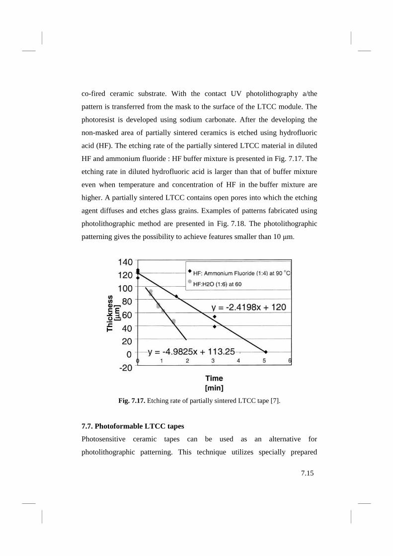
7.15
co-fired ceramic substrate. With the contact UV photolithography a/the
pattern is transferred from the mask to the surface of the LTCC module. The
photoresist is developed using sodium carbonate. After the developing the
non-masked area of partially sintered ceramics is etched using hydrofluoric
acid (HF). The etching rate of the partially sintered LTCC material in diluted
HF and ammonium fluoride : HF buffer mixture is presented in Fig. 7.17. The
etching rate in diluted hydrofluoric acid is larger than that of buffer mixture
even when temperature and concentration of HF in the buffer mixture are
higher. A partially sintered LTCC contains open pores into which the etching
agent diffuses and etches glass grains. Examples of patterns fabricated using
photolithographic method are presented in Fig. 7.18. The photolithographic
patterning gives the possibility to achieve features smaller than 10 μm.
Fig. 7.17. Etching rate of partially sintered LTCC tape [7].
7.7. Photoformable LTCC tapes
Photosensitive ceramic tapes can be used as an alternative for
photolithographic patterning. This technique utilizes specially prepared
7.15

7.16
LTCC tape. Composition of the photoformable ceramic tape is similar to a
standard LTCC tape, however, the photoformable ceramics incorporates,
besides the plasticizers and anifloculants, a photopolymer in the organic
binder. The processing sequence for the photoformable ceramic tape is
depicted in Fig. 7.19.
Fig. 7.18. Patterns fabricated using a/the photolithographic method [7].
Fig. 7.19. Process sequence for photosensitive LTCC tape [7].
7.16

7.17
It consists of few steps. First the photosensitive LTCC tape is laminated to
a rigid glass substrate and baked. Next the tape is exposed to UV light using
contact photolithography. After exposure to UV light, a sodium carbonate
solution is used to remove the unexposed surface area. The depth of etching
can be easily controlled by modifying the development process parameters
like sodium carbonate jet pressure and developing time. The influence of the
sodium carbonate jet pressure and development time on the etching rate of the
photoformable LTCC tape is presented in Fig. 7.20.
Fig. 7.20. Depth of cavity vs. development time and sodium carbonate jet pressure
(PSI -Pound per square inch, 1 PSI = 6894 Pa) [7].
After etching the ceramic tape can be laminated and co-fired. This techniques
allows one to achieve feature sizes smaller than 30 μm. Exemplary pattern
made in photosensitive LTCC tape is presented in Fig. 7.21.
7.17

7.18
Fig. 7.21. Exemplary pattern fabricated in photoformable LTCC tape [7].
7.8. Sacrificial volume material
Enclosed unfilled volumes (chambers, cavities, channels etc.) can be
fabricated in a single green LTCC tape or laminate using one of the above-
mentioned structuration techniques. However, the conventional high pressure
lamination methods (thermo-compression) pose some problems for defining
such volumes. High pressure and temperature of the isostatic or uniaxial
lamination strongly affect the geometry of the final spatial structure and
preclude realization of complex three-dimensional features such as: channels,
cavities, membranes etc. Deformations of the spatial structures can be
reduced by applying conventional thermo-compression lamination in
conjunction with a special filler material (sacrificial volume material, SVM).
This material is a temporary insert which supports and/or defines spatial
structure during high pressure lamination process. As the SVMs different
types of substances can be applied: wax, graphite-based layers, polymers and
mineral materials. Depending on the applied sacrificial volume material its
elimination from the LTCC module takes place either by dissociation during
burnout and sintering (polymers, graphite-based layers) or by etching or
pouring out after firing (mineral materials). In the methods which are based
on the applying of SVM inserts, the fluidic structures are fabricated using two
7.18

7.19
common techniques: ”define and fill” and ”collate and laminate”. A flow-
chart of the ”define and fill” technique is presented in Fig. 7.22. In a ”define
and fill” [12, 13] technique a microchannel is first created by laser cutting or
mechanical milling in the middle layer. The cutting process is followed by an
initial lamination of the middle and bottom layers in an isostatic or uniaxial
press at a relatively low pressure of about 1 MPa, at room temperature. In the
next step, the created microchannel is filled with a sacrificial volume material
and can be sealed by the upper layer (Fig. 7.22b).
a)
b)
Fig. 7.22. Fabrication of (a) surface and (b) buried channels in LTCC module
using “define and fill” process.
7.19

7.20
The SVM is a discrete layer matching with the opening in the middle tape.
The channel is filled in by screen-printing of the SVM paste through mask
made in the backing polymer. The sacrificial volume material deposition
process is referred to in the literature as a screeding. The SVM paste
screeding process is presented in Fig. 7.23.
Fig. 7.23. Screeding process of the SVM paste [14].
The backing polymer with punched or cut openings is used as a mask and a
screen-printer’s squeegee fills the channel with SVM paste. Application of
the backing polymer as a form decreases the number of the process steps
because there is no need to make a stencil or pattern on the screen. Moreover,
the SVM paste shrinkage after drying and backing the polymer ensures
proper thickness of the dried sacrificial insert. Finally, the LTCC module is
laminated second time in an isostaic or uniaxial press with standard thermo-
compression lamination process parameters. After the lamination the ceramic
laminate is co-fired in air. It is recommended to modify the burnout cycle to
insure a complete burnout of the applied temporary insert. Commercially
available sacrificial volume materials are made of graphite because of its
inherent features. Graphite is known to burn away in air above about 600oC,
7.20

7.21
which is intermediate between the debinding and sintering temperatures of
LTCC. It does not react with LTCC and can be easily applied as a thick-film
paste or tape. During firing the graphite is removed according to the
reaction (7.1):
(7.1)
Ideally, a graphite-based sacrificial volume material should be completely
removed below the temperature where the open porosity of LTCC is closed
by densification (about 800oC). Therefore, the co-firing thermal profile
should be modified by applying a slower ramp rate to 850oC or additional iso-
thermal heating stage for carbon burnout. Misfit thermal profile may lead to
swelling or cracking of the LTCC material. Top and cross-sectional views of
an embedded cavity fabricated using standard co-firing profile and a co-firing
profile with an additional iso-thermal heating for carbon burnout is presented
in Fig. 7.24.
Fig. 7.24. Top and cross-sectional views of an embedded cavity fabricated using: (a
,b) a standard co-firing profile and (c, d) a co-firing profile with an additional iso-
thermal heating cycle [10].
7.21
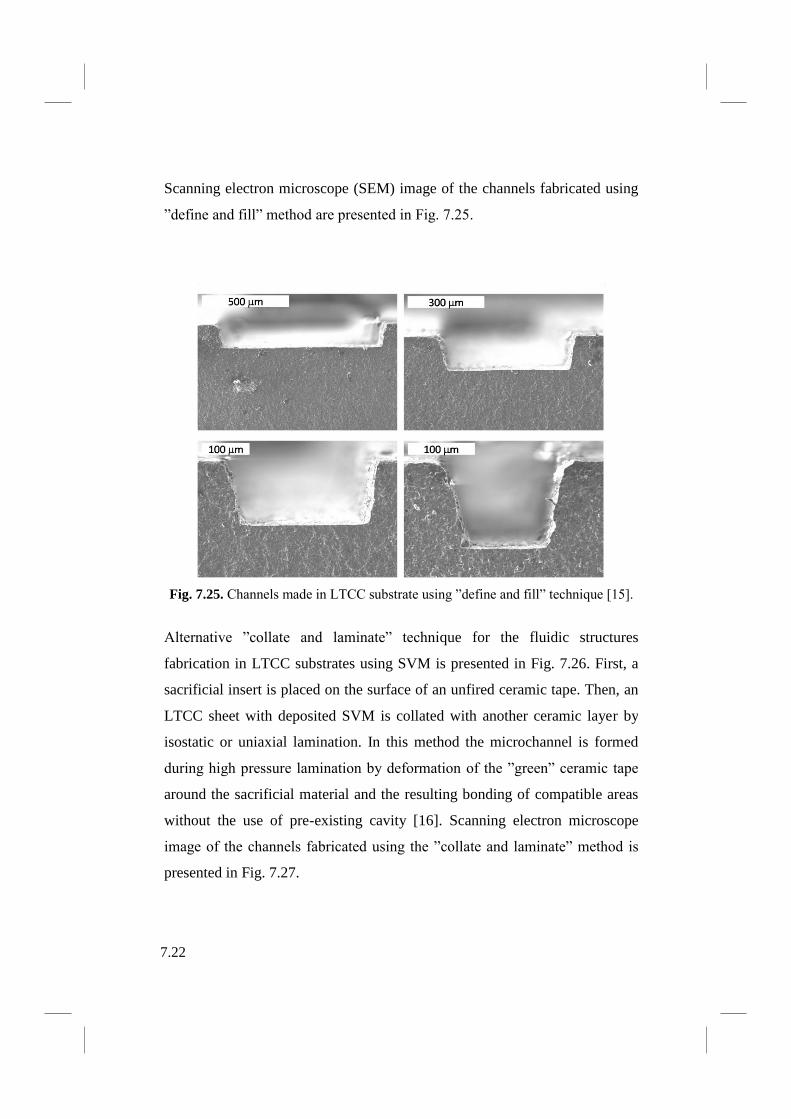
7.22
Scanning electron microscope (SEM) image of the channels fabricated using
”define and fill” method are presented in Fig. 7.25.
Fig. 7.25. Channels made in LTCC substrate using ”define and fill” technique [15].
Alternative ”collate and laminate” technique for the fluidic structures
fabrication in LTCC substrates using SVM is presented in Fig. 7.26. First, a
sacrificial insert is placed on the surface of an unfired ceramic tape. Then, an
LTCC sheet with deposited SVM is collated with another ceramic layer by
isostatic or uniaxial lamination. In this method the microchannel is formed
during high pressure lamination by deformation of the ”green” ceramic tape
around the sacrificial material and the resulting bonding of compatible areas
without the use of pre-existing cavity [16]. Scanning electron microscope
image of the channels fabricated using the ”collate and laminate” method is
presented in Fig. 7.27.
7.22

7.23
Fig. 7.26. A flow-chart of the ”collate and laminate” technique.
Fig. 7.27. Channels made in LTCC substrate using
”collate and laminate” technique [15].
7.23

7.24
Other structures that can be made using a combination of unfired LTCC tape,
sacrificial volume material and high pressure lamination are presented in
Fig. 7.28.
Fig. 7.28. Structures resulting from SVM incorporation in LTCC [14].
By printing thick film pastes onto SVM which is removed during firing it is
possible to manufacture tensile bars (Fig. 7.28a and 7.28b), conductors posts
(Fig. 7.28c), membranes (Fig. 7.28d and 7.28e) and suspended thick film
features (Fig. 7.28f-h). ”Define and fill” and ”collate and laminate”
techniques allowone to fabricate spatial structures with the feature size from
100 μm to a few centimetres in a LTCC substrate.
7.9. Low pressure lamination methods
The thermo-compression is commonly used for laminating ”green” ceramic
tapes. In this technique ceramic layers are stacked and pressed with a high
pressure (5 −30 MPa) at elevated temperature (25−90oC) for 1–20 minutes.
7.24

7.25
The temperature of the process should be set above glass transition point of
the ceramic tape’s organic binder. In order to achieve a homogeneous
junction between ”green” ceramic sheets it is crucial to ensure good
interpenetration of the glass/ceramic particles. Appropriate ratio of
glass/ceramic particles to organic binder facilitate interpenetration of the
particles between ceramic tapes, leading to defect-free homogeneous body
[17]. The thermo-compression lamination results in strong bonding, allowing
good encapsulation of LTCC structures. However, the high pressure and
temperature may affect the geometry of the fluidic structures and damage the
final device. In order to avoid deformations of the spatial structures a special
low pressure lamination methods have been developed. In contrast to a
standard thermo-compression lamination process in a progressive lamination
process each ceramic layer is individually laminated with an isostaic or
uniaxial press to the previous layer to assure a good bond between the
individual LTCC tapes (Fig. 7.29). Thanks to applying the progressive
lamination it is possible to reduce pressure of the process (below 7 MPa). It
was proven that this value of pressure is adequate to bond ceramic tapes
together, prevent layers separation and avoid the deformation of the spatial
structures that could occur at standard lamination pressure [18].
Fig. 7.29. Principle of the progressive lamination process.
Cold low pressure lamination (CLPL) is an advanced method of green
ceramic tapes joining. In contrast to previously described thermo-
compression technique, in which the junction is produced at elevated
7.25
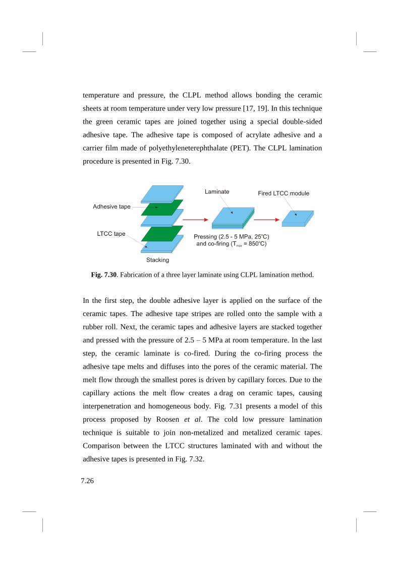
7.26
temperature and pressure, the CLPL method allows bonding the ceramic
sheets at room temperature under very low pressure [17, 19]. In this technique
the green ceramic tapes are joined together using a special double-sided
adhesive tape. The adhesive tape is composed of acrylate adhesive and a
carrier film made of polyethyleneterephthalate (PET). The CLPL lamination
procedure is presented in Fig. 7.30.
Fig. 7.30. Fabrication of a three layer laminate using CLPL lamination method.
In the first step, the double adhesive layer is applied on the surface of the
ceramic tapes. The adhesive tape stripes are rolled onto the sample with a
rubber roll. Next, the ceramic tapes and adhesive layers are stacked together
and pressed with the pressure of 2.5 – 5 MPa at room temperature. In the last
step, the ceramic laminate is co-fired. During the co-firing process the
adhesive tape melts and diffuses into the pores of the ceramic material. The
melt flow through the smallest pores is driven by capillary forces. Due to the
capillary actions the melt flow creates a drag on ceramic tapes, causing
interpenetration and homogeneous body. Fig. 7.31 presents a model of this
process proposed by Roosen et al. The cold low pressure lamination
technique is suitable to join non-metalized and metalized ceramic tapes.
Comparison between the LTCC structures laminated with and without the
adhesive tapes is presented in Fig. 7.32.
7.26

7.27
Fig. 7.31. A model of the melt flow through the smallest pores causing the LTCC
layers to approach each other. The white arrows indicate the flux of the PET melt,
while the black arrows represent the approach of the LTCC layers towards each
other [17].
Fig. 7.32. Comparison between multilayer LTCC structures laminated
(a) with and (b) without adhesive tapes [20].
Cold chemical lamination (CCL) is a solvent-based method of green ceramic
layers joining [21]. The CCL lamination procedure is presented in Fig. 7.33.
The CCL technique is similar to previously presented CLPL lamination
7.27

7.28
method. The difference between the cold chemical lamination and cold low
pressure lamination is that the ceramic tape is covered by a thin film of
a solvent instead of an adhesive layer. The solvent is deposited on the surface
of the LTCC tape using a paint brush or standard screen-printing method.
After deposition of the solvent the ceramic sheets are stacked together and
pressed with a very low pressure of 0.5 MPa at room temperature.
Fig. 7.33. Fabrication of a LTCC-based fluidic structure using CCL lamination
method
The applied solvent dissolves the surface of the two adjacent ceramic tapes
and bonds them together. Since then the LTCC layers cannot be separated. In
the last step, the ceramic module is co-fired in air in a typical two step
thermal profile. During the co-firing process the applied solvent is vaporising
completely leaving no residue. In comparison with the standard thermo-
compression method the CCL technique causes less deformation during the
lamination process. It permits us to achieve fine fluidic structures (channels,
cavities etc.). Exemplary channels fabricated in LTCC substrate using the
CCL methods are presented in Fig. 7.34.
However, this method has three main disadvantages [22]: (i) it cannot be
applied to fabrication of precise spatial structures (~50 μm) due to the etching
of green ceramic tapes during lamination, (ii) solvent that works for one
particular LTCC system might not be suitable for another LTCC material,
7.28

7.29
(iii) the applied solvent may affect the final electrical properties of the screen-
printed conductors and passives [23].
Fig. 7.34. Embedded channels fabricated in LTCC module using CCL method [21].
References
[1] Smetana W, Balluch B, Stangl G, Lüftl S, Seidler S, Processing
procedures for the realization of fine structured channel arrays and
bridging elements by LTCC-technology, Microelectronics Reliability,
49 (2009) 592-599.
[2] Nowak KM, Baker HJ, Hall DR, Cold processing of green state LTCC
with CO2 laser, Applied Physics A, Material Science and Processing, 84
(2006) 267-270.
[3] Nowak D, Miś E, Dziedzic A, Kita J, Fabrication and electrical
properties of laser-shaped thick-film and LTCC microresistors,
Microelectronics Reliability, 49 (2009) 600-606.
[4] Kita J, Dziedzic A, Golonka LJ, Zawada T, Laser treatment of LTCC
for 3D structures and elements fabrication, Microelectronics
International, 19 (2002) 14-18.
7.29

7.30
[5] Hagen G, Laser processing of ceramic green tape, Workshop on tape
3D structuring, Orbassano-Turin (Italy), November 2010.
[6] Wang G, Folk EC, Barlow F, Elshabini A, Fabrication of microvias for
multilayer LTCC substrates, IEEE Transactions on Electronics
Packaging Manufacturing, 29 (2006) 32-41.
[7] Gongora-Rubio MR, Espinoza-Vallejos P, Sola-Laguna L, Santiago-
Avilés JJ, Overview of low temperature co-fired ceramics tape
technology for meso-system technology (MsST), Sensors and Actuators
A: Physical, 89 (2001) 222-241.
[8] ZeilmannC, Punching technology, Workshop on tape 3D structuring,
Orbassano-Turin (Italy), November 2010.
[9] Rabe T, Kuchenbecker P, Schulz B, Schmidt M, Hot embossing: an
alternative method to produce cavities in ceramic multilayer,
International Journal of Applied Ceramic Technology, 4 (2007), 38-46.
[10] Khoong LE, Tan YM, Lam YC, Overview on fabrication of three-
dimensional structures in multi-layer ceramic substrate, Journal of the
European Ceramic Society, (30) 2010 1973-1987.
[11] Andrijasevic D, Smetana W, Zehetner J, Zoppel S, Brenner W, Aspects
of micro structuring low temperature co-fired ceramic (LTCC) for
realisation complex 3D objects by embossing. Microelectronic
engineering, 84 (2007) 1198-1201.
[12] Malecha K, Golonka LJ, Microchannel fabrication process in LTCC
ceramics. Microelectronics Reliability, 48 (2008) 866-871.
[13] Malecha K, Golonka LJ, Three-dimensional structuration of zero-
shrinkage LTCC ceramics for microfluidic applications,
Microelectronics Reliability, 49 (2009) 585-591.
[14] Peterson KA, Knudson RT, Garcia EJ, Patel KD, Okandan M, Ho CK,
James CD, Rohde SB, Rohrer BR, Smith F, Zawicki LR, Wroblewski
7.30

7.31
BD, LTCC in microelectronics, microsystems and sensors, Proc. 15th
IEEE International Conference MIXDES, Poznań (Poland), June 2008,
23-37.
[15] Malecha K, Maeder T, Jacq C, Ryser P, Structuration of the low
temperature co-fired ceramics (LTCC) using novel sacrificial paste with
PVA-propylene glycol-glycerol-water vehicle, Microelectronics
Reliability, 51 (2011) 805-811.
[16] Peterson KA, Patel KD, Ho CK, Rohde SB, Nordquist CD, Walker CA,
Wroblewski BD, Okandan M, Novel microsystem applications with
new techniques in low-temperature co-fired ceramics, International
Journal of Applied Ceramic Technology, 2 (2005) 345-363.
[17] Piwonski M, Roosen A, Low pressure lamination of ceramic green
tapes by gluing at room temperature, Journal of the European Ceramic
Society, 19 (1999) 263-270.
[18] Barlow F, Wood J, Elshabini A, Stephens EF, Feeler R, Kenner G,
Junghans, Fabrication of precise fluidic structures in LTCC,
International Journal of Applied Ceramic Technology, 6 (2009) 18-23.
[19] Roosen A, New lamination technique to join ceramic green tapes for
the manufacturing of multilayer devices, Journal of the European
Ceramic Society, 21 (2001) 1993-1996.
[20] Schindler K, Roosen A, Manufacture of 3D structures by cold low
pressure lamination of ceramic green tapes, Journal of the European
Ceramic Society, 29 (2009) 899-904.
[21] Jurków D, Roguszczak H, Golonka L, Cold chemical lamination of
ceramic green tapes, Journal of the European Ceramic Society, 29
(2009) 703-709.
[22] Malecha K, Jurków D, Golonka LJ, Comparison of solvent and
sacrificial volume material based lamination processes of low
7.31

7.32
temperature co-fired ceramics (LTCC) tapes, Journal of
Micromechanics and Microengineering, 19 (2009) 065022.1-
065022.10.
[23] Jurków D, Golonka LJ, Novel cold chemical lamination bonding
technique – a simple LTCC thermistor-based flow sensor, Journal of the
European Ceramic Society, 29 (2009) 1971-1976.
7.32

8.1
Chapter 8
Bonding techniques of the LTCC with different materials
8.1. Introduction
Low temperature co-fired ceramic technology is hybrid in nature. The LTCC
material can be easily bonded with different materials. Developing of the
LTCC-silicon [1, 2], LTCC-glass [3, 4], LTCC-polymer (PDMS,
polydimethylosiloxane) [5] and LTCC-ceramics bonding technologies has
expanded the frontiers of LTCC appliances.
8.2. LTCC-Si
The LTCC ceramics can be bonded with silicon structures using an anodic
bonding [6]. The main advantages of the application of LTCC technology for
the fabrication of anodic bondable substrates are:
• multi-functionality with 3D interconnected multilayer substrate,
• ceramic multilayer packaging structure with hermetic packaging
between Si chip and LTCC,
• reduction of packaging size with direct interconnections between a
chip and a package
• use of standard thick film technology,
• possibility of local bonded areas: the size of the bonded area can be
controlled by structuring of LTCC surface in green or sintered state,
• Possibility of passive components integration (to move passives from
expensive chip area into the LTCC area).
Anodic bonding is a well known process of sealing Si substrate to a plain
glass wafer (Pyrex 7740). The process takes place in the voltage range of 400
– 1000 V and at elevated temperature (about 400oC). The anodic bonding
process is shown in Fig. 8.1.
8.1

8.2
A glass wafer is biased negatively while silicon is polarized positively.
Sodium cations within, move through the glass wafer to the cathode. In a
consequence of the sodium ions transport a depletion layer is forming in the
vicinity of the anode. The generated electric field causes the motion of the
oxygen anions, which leads to the formation of an oxide layer at the metallic
interface. In order to obtain the bonding between silicon and LTCC material
three main conditions have to be fulfill:
1. the coefficient of thermal expansion (CTE) of the LTCC substrate
must be matched to the CTE of silicon (CTE difference between both
materials in the temperature range from 25oC to 400
oC should be less
than ± 0.2 ppm/K),
2. the LTCC substrate should contain appropriate concentration of the
sodium ions (1-2 wt %),
3. the LTCC surface roughness should be less than 100 nm.
Fig. 8.1. Anodic bonding process.
The commercially available LTCC does not contain the alkali ions necessary
for anodic bonding that are indispensable to realize the ionic migration
between a silicon wafer and ceramic substrate. However, LTCC can be
anodic bonded to silicon through a thin film of bondable screen-printed
8.2

8.3
glass [1]. The LTCC to Si bonding process through the layer of bondable
glass is presented in Fig. 8.2. The main drawback of the applying of screen-
printable glass is CTE mismatch between the LTCC and silicon which may
cause cracking during the cooling down.
Fig. 8.2. LTCC to silicon bonding process using a bondable glass layer.
Another approach was proposed by German company VIA Electronics GmbH
[7]. They have developed anodic bondable LTCC green tape system
(BGK79). The new LTCC tape is composed of borosilicate glass, alumina
and cordierite. This composition has a Na+ ions content of 1.7 wt%. The CTE
of the anodic bondable LTCC material is matched with silicon (Fig. 8.3).
Fig. 8.3. Comparison of CTE for silicon, anodic bondable LTCC (BGK79) and
Borofloat glass [7].
8.3

8.4
However, the LTCC material requires additional polishing step in order to
achieve appropriate surface roughness (< 100 nm) and flatness
(< 5 m/10 mm). The ceramic tape system developed by VIA Electronics
GmbH is compatible with Au metallization. Scanning electron microscope
image of the LTCC/Si interface is presented in Fig. 8.4. A comparison
between both LTCC-Si anodic bonding procedures is given in Table 8.1.
Fig. 8.4. Cross-section of anodic bonded LTCC with silicon (SEM image) [7].
Table 8.1. Comparison between Si-LTCC bonding methods.
Technique Advantages: Disadvantages: LTCC covered with
anodic bondable thick-
film glass
Compatible with standard
thick-film pastes
No polishing is required
(Ra ~ 20 nm)
Additional screen-printing
and post-firing steps
LTCC/Si structure may
crack during cooling down
step (CTE mismatch)
Anodic bondable LTCC
material Compatible with thick-
film (Au) metallization
system
CTE of the LTCC tape
matched to CTE of Si
No additional printing and
firing is required
Additional polishing is
required
Not compatible with all
thick-film metallization
systems
8.4

8.5
8.3. LTCC-glass
A serious limitation of the LTCC-based microsystems is non-transparency of
the ceramic material. In many cases it is necessary to observe the phenomena
that take place inside the microfluidic system during the operation (such as
mixing, colour changing, fluorescence, transport of the particles suspended in
the flowing medium). The non-transparent ceramic cover makes this type of
investigation impossible. A sapphire glass can be easily integrated with a
ceramic structure using the standard LTCC technology [8]. Flow-chart of a
sapphire glass to LTCC ceramic bonding process is presented in Fig. 8.5.
Fig. 8.5. A flow-chart of sapphire glass to LTCC ceramic bonding process.
A glass plate is laminated with LTCC tapes during an isostatic or uniaxial
lamination process. The channel placed below the sapphire glass is defined by
a SVM insert. After lamination the structure is co-fired in air according to the
typical two-step thermal profile. Thanks to matching of the coefficient of
thermal expansion of LTCC and sapphire glass the stress induced during the
8.5

8.6
co-firing process is negligible. The sapphire glass/LTCC based structure is
hermetic, it is characterized by helium leakproofness. Exemplary hybrid
glass-LTCC structures fabricated using the sapphire glass are presented in
Fig. 8.6.
Fig. 8.6. Sapphire glass-LTCC hybrid structures [3].
A slightly different approach was proposed by Bembnowicz et al [4]. The
technological process flow, presented in Fig. 8.7, is similar to sapphire glass
to LTCC ceramic bonding Process, however, the technique does not allow the
application of high pressure. The LTCC tapes and glass window have to be
initially bonded using a cold low pressure lamination or cold chemical
lamination process. A key in this method lies in the application of glass with
the softening temperature in the range of 670-720oC. Thanks to this, the glass
plate becomes soft during the co-firing process before the LTCC shrinkage
starts. The surface tension of the liquid glass membrane is sufficient to
balance the gravity force. The surface tension force holds the soft glass
membrane spread over the fluidic structure. As the temperature decreases the
glass membrane vitrification is initiated and a dense and transparent material
8.6
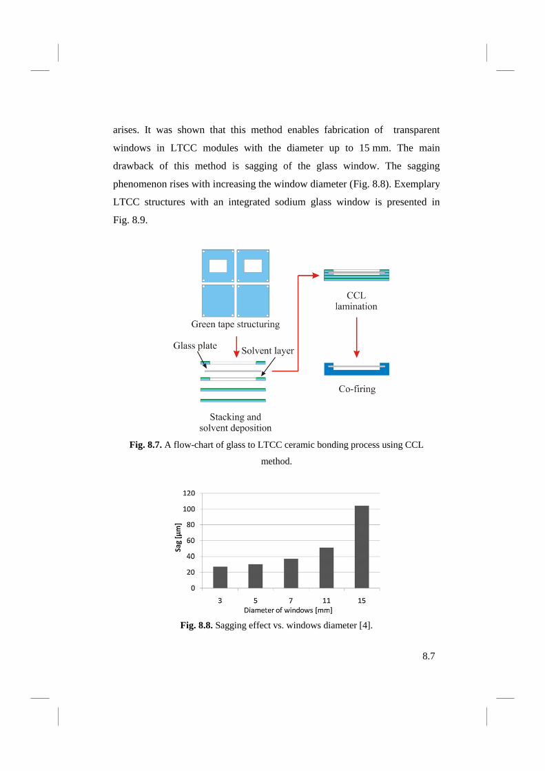
8.7
arises. It was shown that this method enables fabrication of transparent
windows in LTCC modules with the diameter up to 15 mm. The main
drawback of this method is sagging of the glass window. The sagging
phenomenon rises with increasing the window diameter (Fig. 8.8). Exemplary
LTCC structures with an integrated sodium glass window is presented in
Fig. 8.9.
Fig. 8.7. A flow-chart of glass to LTCC ceramic bonding process using CCL
method.
Fig. 8.8. Sagging effect vs. windows diameter [4].
8.7

8.8
Fig. 8.9. LTCC structures integrated with sodium glass window [4].
8.4. LTCC-PDMS
The microsystems made by the hybrid glass/LTCC technique exhibit some
technological limitations. Because of very high (> 850oC) encapsulation
temperature of the glass-ceramic modules it is impossible to place
temperature-sensitive (bio)chemical agents (e.g. catalytic bed, enzyme carrier
or polymeric receptor layer) inside the LTCC-based microfluidic device.
A solution of this problem can be the technique using plasma assisted
bonding of LTCC to transparent polymer (PDMS). A hybrid PDMS/LTCC
microsystem takes advantage of the both materials. On one hand, fine fluidic
structures can be made in a transparent polymer lid using laser
micromachining, hot embossing or soft lithography. On the other hand,
a ceramic substrate with integrated conductors, passives, MEMS devices,
actuators, optoelectronics components and fluidic structure can be fabricated
using the LTCC technology. The general manufacturing process of the hybrid
polymeric/ceramic microsystem is presented in Fig. 8.10. In the first step,
a PDMS plate is prepared using two-component mixture (prepolymer and
cross-linking agent).
8.8

8.9
Fig. 8.10. A flow-chart of LTCC-PDMS bonding process [9].
After cross-linking process the fluidic structures can be fabricated in the
polymeric substrate. Simultaneously, the LTCC multilayer substrate is
manufactured according to a standard technological process. After co-firing
the ceramic structure is covered by a thin glaze film using the screen-printing
method. Then the glass-covered LTCC module is post-fired in air at
temperature the of 875oC for 60 minutes. The glaze layer is applied to
eliminate microporosity of the fired LTCC material. In the next step, the
surfaces of both materials are activated using microwave oxygen [9] or argon
[10] plasma. The plasma generates free radicals and causes formation of
silanol groups (Si−OH) on the PDMS surface as it is presented in Fig. 8.11.
On the glass surface there are some hydroxyl and other oxygen-containing
groups that are created during the glass firing process. During the cooling
down the melted glass absorbs water from the surroundings. The energy of
8.9

8.10
the plasma is big enough to break the hydrogen bonds between the water
molecules. The applied microwave plasma divides the O-OH bond into
atomic oxygen and additional hydroxyl radicals as shown in Fig. 8.12.
Fig. 8.11. Change in the molecular structures of the PDMS surface after plasma
treatment [11].
Fig. 8.12. Change in the molecular structures of the glass surface after plasma
treatment [12].
Fig. 8.13. PDMS/LTCC microfluidic structures [5].
8.10

8.11
After putting the modified sides of the both materials into contact, Si−O−Si
covalent bond is formed as a result of condensation reaction between the
silanol groups. Exemplary PDMS/LTCC hybrid structures are presented in
Fig. 8.13.
8.5. LTCC-ceramic
A ceramic substrate can be bonded to a fired LTCC structure using low
temperature glass layer. The flow-chart of the bonding process is presented in
Fig. 8.14. In the first step, the ceramic substrate and the LTCC module are
covered with a glaze layer. Then the glass-covered surfaces of the materials
are put into contact and heated above glass transition temperature. As
the temperature decreases the glass layer forms a hermetic bond between the
both ceramic substrates. The ceramic structures fabricated using the low
temperature glass layer are presented in Fig. 8.15.
Fig. 8.14. The bonding process of sintered LTCC to ceramic plate.
Fig. 8.15. (a) Ion mobility spectrometer drift tube and (b) seven segment stack
fabricated using LTCC-LTCC bonding technique [13].
8.11

8.12
References
[1] Bergstedt L, Persson K, Printed glass for anodic bonding - a packaging
concept for MEMS and system on a chip, Advancing Microelectronics,
29 (2002) 1-4.
[2] Khan MF, Ghavanini FA, Haasl S, Löfgren L, Persson K, Rusu C,
Schjólberg-Henriksen K, Enoksson P, Methods for characterization of
wafer-level encapsulation applied on silicon to LTCC anodic bonding,
Journal of Micromechanics and Microengineering, 20 (2010),
064020.1-064010.10.
[3] Peterson KA, Knudson RT, Garcia EJ, Patel KD, Okandan M, Ho CK,
James CD, Rohde SB, Rohrer BR, Smith F, Zawicki LR, Wroblewski
BD, LTCC in microelectronics, microsystems and sensors, Proc. 15th
IEEE International Conference MIXDES, Poznań (Poland), June 2008,
23-37.
[4] Bembnowicz P, Golonka LJ, Integration of transparent glass window
with LTCC technology for μTAS application, Journal of the European
Ceramic Society, 30 (2010) 743-749.
[5] Chudy M, Malecha K, Golonka LJ, Sosicki A, Roguszczak H,
Jakubowska M, Dybko A, Brzózka, Z, Bonding technique of polymer
layer with ceramic elements of analytical microsystems, Proc. of SPIE,
6348 (2006) P1-P4.
[6] Dziuban JA, Bonding in microsystem technology, Springer,
Netherlands, 2006.
[7] Müller E, Bartnitzek T, Bechtold F, Pawlowski B, Rothe P, Ehrt R,
Heymel A, Weiland E, Schröter T, Schundau S, Kaschlik K,
Development and processing of an anodic bondable LTCC tape. Proc.
1st International Conference and Exhibition on Ceramic Interconnect
8.12

8.13
and Ceramic Microsystem Technologies, Baltimore (USA), April 2005,
53-58.
[8] Peterson KA, Rohde SB, Walker CA, Patel KD, Turner TS, Nordquist
CD, Microsystem integration with new techniques in LTCC. Proc.
IMAPS Conference and Exhibition on Ceramic Interconnect
Technology: The Next Generation II, Denver (USA), April 2004, 19-
26.
[9] Malecha K, Gancarz I, Golonka LJ, A PDMS/LTCC bonding technique
for microfluidic application. Journal of Micromechanics and
Microengineering, 19 (2009) 105016.1-105016.8.
[10] Malecha K, Gancarz I, Tylus W, Argon plasma-assisted PDMS-LTCC
bonding technique for microsystem applications. Journal of
Micromechanics and Microengineering, 20 (2010) 115006.1-115006.8.
[11] Haines SR, Beamson G, Williams RL, Weightman P, Changes in the
electronic structure of silicone rubber surface induced by oxygen
plasma treatment, Surface and Interface Analysis, 39 (2007) 942-947.
[12] Wang C, He X, Preparation of hydrophobic coating on glass surface by
dielectric barrier discharge using 16 kHz power supply, Applied
Surface Science, 252 (2006) 8348-8351.
[13] Weston H, Plumlee DG, Moll AJ, Post-bonding and fabrication of low
temperature co-fired ceramic, Proc. 3rd International Conference and
Exhibition on Ceramic Interconnect and Ceramic Microsystem
Technologies, Denver (USA), April 2007, 320-323.
8.13

8.14
8.14

9.1
Chapter 9
LTCC-based microfluidic systems
9.1. Introduction
The modern microfluidic systems consist of several functional blocks (sub-
systems). Those sub-systems are responsible for sample transport
(micropumps, microvalves), preliminary preparation of the sample
(micromixers), carrying out appropriate (bio)chemical reaction
(microreactors), product separation and detection of the analyte
(electrochemical and/or optical sensors). In this chapter, a briefly description
of construction and principle of operation of various ceramic-based
microfluidic sub-systems is given.
9.2. Microvalves and micropumps
Microvalves and micropumps cannot be fabricated as monolithic ceramic
structures. These devices are made as hybrid structures. The moving part,
usually a membrane, is made of silicon or steel. Actuation of the membrane
can be made according to the piezoelectric or electromagnetic principle.
Piezoelectric action
Piezoelectricity is an inherent property of a certain group of materials. This
feature can be described as a correlation between mechanical and electrical
behaviour of these materials. More precisely, applying of mechanical pressure
to piezoelectric material produces a small voltage proportional to the applied
pressure. Conversely, applying of electric field causes minute dimensional
changes in the material [1]. In a microscopic scale, piezoelectricity is a result
of non-uniform charge distribution within the unit cell of a crystal. In
a consequence of crystal mechanical deformation the positive and negative
9.1

9.2
charge centres displace by different amounts. Although the overall crystal
remains electrically neutral, the variation in the charge centre displacement
causes electrical polarization within a crystal structure. This polarization
caused by mechanical input is perceived as piezoelectricity [2]. Piezoelectric
properties are induced in the ceramics during electrical poling. The poling
process is performed at elevated temperature (150oC) in a silicon oil bath.
Electrical poling sets mechanical and electrical axes of orientation. When the
electric field is applied, the piezoceramics expands along the axis of the field
and contracts perpendicular to it (Fig. 9.1).
Fig. 9.1. Effect of poling on the dimensions of piezoelectric material [1].
After the poling process the piezoceramics dimensions can be changed, by
applying a voltage less than the poling voltage. Dimensional change will be
sustained as long as the voltage is applied. Fig. 9.2 illustrates a piezoceramics
motor action: conversion of electrical to mechanical energy. An electrically
poled ceramics without any applied voltage is presented in Fig. 9.2a.
Applying a voltage with polarity matched with the poling voltage results in an
additional expansion along the poling axes and contraction perpendicular to it
9.2
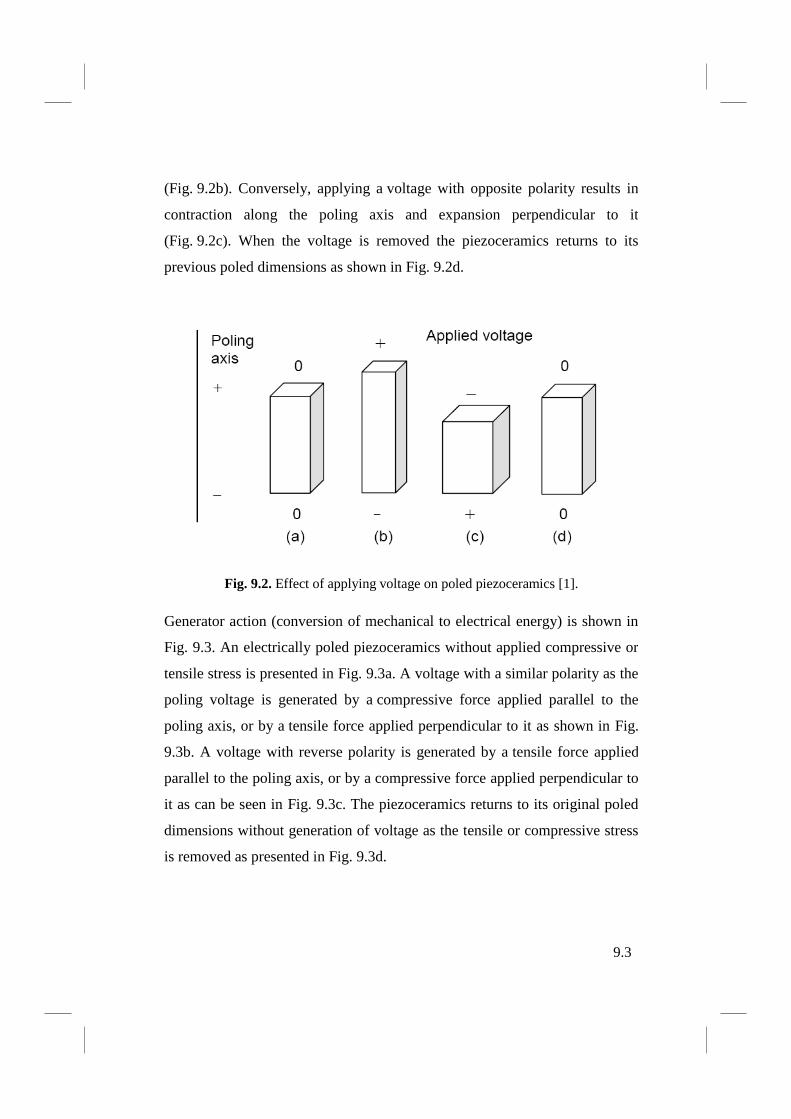
9.3
(Fig. 9.2b). Conversely, applying a voltage with opposite polarity results in
contraction along the poling axis and expansion perpendicular to it
(Fig. 9.2c). When the voltage is removed the piezoceramics returns to its
previous poled dimensions as shown in Fig. 9.2d.
Fig. 9.2. Effect of applying voltage on poled piezoceramics [1].
Generator action (conversion of mechanical to electrical energy) is shown in
Fig. 9.3. An electrically poled piezoceramics without applied compressive or
tensile stress is presented in Fig. 9.3a. A voltage with a similar polarity as the
poling voltage is generated by a compressive force applied parallel to the
poling axis, or by a tensile force applied perpendicular to it as shown in Fig.
9.3b. A voltage with reverse polarity is generated by a tensile force applied
parallel to the poling axis, or by a compressive force applied perpendicular to
it as can be seen in Fig. 9.3c. The piezoceramics returns to its original poled
dimensions without generation of voltage as the tensile or compressive stress
is removed as presented in Fig. 9.3d.
9.3
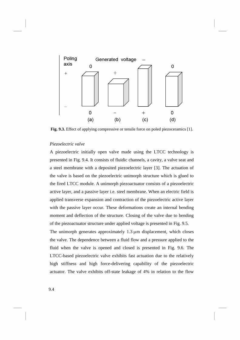
9.4
Fig. 9.3. Effect of applying compressive or tensile force on poled piezoceramics [1].
Piezoelectric valve
A piezoelectric initially open valve made using the LTCC technology is
presented in Fig. 9.4. It consists of fluidic channels, a cavity, a valve seat and
a steel membrane with a deposited piezoelectric layer [3]. The actuation of
the valve is based on the piezoelectric unimorph structure which is glued to
the fired LTCC module. A unimorph piezoactuator consists of a piezoelectric
active layer, and a passive layer i.e. steel membrane. When an electric field is
applied transverse expansion and contraction of the piezoelectric active layer
with the passive layer occur. These deformations create an internal bending
moment and deflection of the structure. Closing of the valve due to bending
of the piezoactuator structure under applied voltage is presented in Fig. 9.5.
The unimorph generates approximately 1.3 m displacement, which closes
the valve. The dependence between a fluid flow and a pressure applied to the
fluid when the valve is opened and closed is presented in Fig. 9.6. The
LTCC-based piezoelectric valve exhibits fast actuation due to the relatively
high stiffness and high force-delivering capability of the piezoelectric
actuator. The valve exhibits off-state leakage of 4% in relation to the flow
9.4

9.5
rate of the open valve due to surface roughness and LTCC distortion
preventing complete sealing of the valve by the membrane.
Fig. 9.4. LTCC-based piezoelectric valve [3].
Fig. 9.5. Cross-section of the piezoelectric LTCC valve, not in scale [3].
9.5
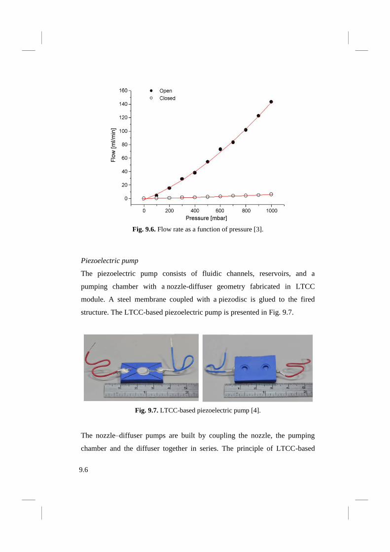
9.6
Fig. 9.6. Flow rate as a function of pressure [3].
Piezoelectric pump
The piezoelectric pump consists of fluidic channels, reservoirs, and a
pumping chamber with a nozzle-diffuser geometry fabricated in LTCC
module. A steel membrane coupled with a piezodisc is glued to the fired
structure. The LTCC-based piezoelectric pump is presented in Fig. 9.7.
Fig. 9.7. LTCC-based piezoelectric pump [4].
The nozzle–diffuser pumps are built by coupling the nozzle, the pumping
chamber and the diffuser together in series. The principle of LTCC-based
9.6

9.7
piezoelectric pump operation is based on the nozzle-diffuser pumping
phenomenon (Fig. 9.8). The volume of fluid in the pumping chamber is
periodically varied using an oscillating pressure. Variation of the pressure is
provided by a frequent deflection of the steel membrane induced by
contraction and expansion of the piezodisc supplied with AC voltage.
Fig. 9.8. Principle of operation of a nozzle–diffuser pump [5].
The kinetic energy of the fluid (velocity) is converted to the potential energy
(pressure) both in the nozzle and diffuser but the efficiency of this process is
much greater in the diffuser direction thus discharging more fluid through the
diffuser. If Qd is the discharge through the diffuser and Qn is the discharge
through the nozzle then an increase in the chamber volume causes Qd > Qn
and a decrease in the chamber volume causes Qd < Qn resulting in a net
9.7

9.8
pumping action [5]. The mean value of fluid flow and displacement of the
membrane as a function of applied AC voltage frequency is presented in
Fig. 9.9. Nuzzle/ Nozzle-diffuser pumps cannot generate large pressure and
are suitable for low-pressure fluidic systems.
Fig. 9.9. Flow rate and piezoactuator displacement amplitude vs frequency of the AC
voltage [4].
Electromagnetic actuation
Forces of magnetic origin are generated by the interaction of a magnetic field
with an electrical current [6]. For a vertical actuation, which is commonly
used in case of microvalves and micropumps, the force generated by the
interaction between magnetic field with intensity Hz created by a current I
which flows through a coil and a permanent magnet with magnetization Mz is
equal to:
9.8

9.9
(9.1)
therefore, the generated force depends on the Hz variation. When the magnet
is placed on a flexible spring then the applied force will be equal to:
(9.2)
As a result of this force, the spring generates a displacement z which is
proportional to the force divided by the equivalent spring constant k:
(9.3)
Electromagnetic actuation techniques have numerous advantages [6]:
generation of large force,
production of relatively large displacement,
good performance with temperature,
adequate velocity response,
robust and inexpensive technique.
Electromagnetic valve
A LTCC-based hybrid microvalve with electromagnetic actuation consists of
a multilayer coil, a fluidic channel and a flexible membrane with a permanent
magnet bonded to its top surface. The scheme of the magnetic valve is
presented in Fig. 9.10.
The fluidic part of the valve is made of three ceramic layers (Fig. 9.11).
Layer 1 consists of a fluidic inlet and outlet, a membrane seal and a valve
9.9

9.10
seat. The fluidic channels are made in layer 2. Layer 3 defines the bottom of
the fluidic part.
Fig. 9.10. LTCC-based hybrid magnetic valve [6].
The multilayer coil consists of seven layers of a planar spiral implemented on
LTCC tapes. The flexible diaphragm attached to the LTCC structure is made
of silicon using standard anisotropic etching method. A rare earth magnet
(SmCo) is bonded to a flexible diaphragm during its fabrication process. The
fabricated hybrid microvalve is presented in Fig. 9.12.
Fig. 9.11. Fluidic part of the
magnetic valve [6].
Fig. 9.12. Fabricated hybrid
microvalve [6].
9.10

9.11
Using SmCo magnet with 1 mm diameter it is possible to obtain 200 m
deflection of the 30 m thick silicon rectangular diaphragm [6]. The
dependence between the diaphragm displacement and the current in the coil is
presented in Fig. 9.13.
Fig. 9.13. Flexible diaphragm displacement vs. coil current [6].
Electromagnetic pump
A concept of the LTCC-based electromagnetic micropump and its equivalent
electronic circuit are presented in Fig. 9.14. The device consists of
microfluidic chamber made in the LTCC substrate and a polymeric
membrane coupled with a rare earth magnet and an excitation electromagnet
[7]. The flexible membrane is made of PDMS (polydimethylosiloxane).
The LTCC-based electromagnetic pump utilizes two ball valves which act as
a fluidic diodes and prevent back flow. The applied balls are made of
9.11

9.12
sapphire glass. The principle of LTCC-based electromagnetic pump operation
is depicted in Fig. 9.15.
Fig. 9.14. LTCC-based electromagnetic micropump design and its electronic
equivalent circuit [7].
Fig. 9.15. Principle of operation of LTCC-based electromagnetic pump.
The volume of the fluid in the chamber is periodically varied due to
deflection of the PDMS membrane. The deflection is caused by frequently
changes of the electromagnet polarity. When the membrane goes down
(chamber expansion) the inlet fluidic diode is opened and the fluid is drawn
into the chamber. When the polarity of the electromagnet is changed the
magnetic forces causes a deflection of the membrane. As a result of the
chamber contraction the inlet diode is closing. Simultaneously the outlet
diode is opening and the fluid can be pumped out of the chamber.
9.12

9.13
9.3. Ceramic micromixers
One of the essential parts of a modern microfluidic system is an efficient
micromixer. For example, enzymatic reactions require the intermix of all
reagents for initiations. In general, micromixers can be classified as either
active or passive [8]. An active micromixer requires external energy
(pressure, temperature, electro-hydro-dynamics, acoustics, etc.) to generate
disturbances necessary to achieve efficient mixing process. Contrary to the
active micromixers, the passive mixing structures do not require any external
forces. Their mixing efficiency relies entirely on molecular diffusion and
chaotic advection. The passive micromixers are generally easier to fabricate
and integrate with other microfluidic devices. A good mixing structure should
homogenise two (or more) fluids in micro- or nanoliter volume scale without
taking much space in acceptable time-scales. However, due to very small
dimensions of the microfluidic systems the flow is mostly in laminar regime.
As a consequence, the mass transfer is based mainly on molecular diffusion.
The diffusive mixing process is relatively slow in comparison with the rate at
which fluid is convected along the conduit. This make an effective mixing of
initially segregated fluids difficult. The Péclet number represents the ratio
between the mass transport due to convection and that of diffusion, and is
defined as:
(9.4)
where U is a mean fluid velocity (m/s), Dh is a hydraulic diameter (m) and D
is a coefficient of molecular diffusion (m2/s). It varies from approximately 10
-
9 for small molecules (e.g. water) to 10
-11 for the larger ones (e.g. glucose).
Convection is dominant at higher Péclet number. Typical values of the Pe for
9.13

9.14
microfluidic systems are high and vary from 101 to 10
6 [2, 7]. The Péclet
number can be interpreted as a ratio of diffusive mixing time:
(9.5)
Using equations (6.6) and (9.5) we can infer that fluids which move with a
mean velocity U have to pass through a distance U(D2
h/D) to be completely
mixed. For example, the mixing time and distance required to homogenise the
concentrations at a mean flow velocity of 1 mm/s and a channel hydraulic
diameter of 200 m may vary from 40 s and 0.4 m for a diffusion coefficient
of 10-9
m2/s to 4000 s and 40 m for diffusivity of 10
-11 m
2/s.
The magnitude of the mass flux (J) of the fluid particles due to the molecular
diffusion is equal to:
(9.6)
where c is the concentration [m-3
]. From this equation, it is clearly seen that
the key to efficient mixing in microscale relies mainly on two issues:
1. interface area between two initially segregated fluids,
2. the ability to create high concentration gradients between two mixing
fluids.
On one hand, a larger interface area results in a larger area for mass transfer.
On the other hand, very high concentration gradients accelerate the diffusion
process. Elongation of the intermaterial area and the increase in concentration
gradients can be achieved by stretching and folding phenomena characteristic
for chaotic advection. These effects can be obtained in microfluidics through
the appropriate design of the micromixer’s channel geometry. Spatial changes
along the fluidic channel axes result in frequent changes of flow direction.
9.14

9.15
The mixing process in a microfluidic system can be modeled and visualized
by solving the convection-diffusion equation:
(9.7)
where u = (u, v, w) is the fluid velocity vector in (m/s). The velocity field can
be calculated from the Navier-Stokes equation (6.15).
Magneto-hydro-dynamic(MHD) mixer
The device takes advantage of Lorentz force induced by the coupling between
the magnetic field B and the electrical field E. This force is applied to disturb
the fluid flow pattern within a device. The MHD mixer is made of three
LTCC tapes and a permanent Neodymium magnet. The details of the
particular ceramic layers and cross-section of the device are presented in
Fig. 9.16.
Fig. 9.16. LTCC layers and cross-sectional view of the MHD micromixer [9].
9.15

9.16
Gold electrodes are deposited on layer 1. Layer 2 contains the mixing channel
and two vertical vias for electrical connections. The structure is sealed by
layer 3. The mixing channel is filled with an electrolyte solution. By applying
alternating potential across the pairs of the electrodes, currents are induced in
various directions in the solution. In the presence of a magnetic force
(induced by permanent magnet) the currents generate the Lorentz force in
a perpendicular direction to both magnetic and electrical fields. The direction
of the force alternates according to the changes of the positive and negative
poles of a DC power supply. The Lorentz force is applied to induce mixing
movement of the fluid in the channel. It causes stretching and folding of the
fluid in the mixing channel. As a result, the interface layer (IL) between two
mixing fluids is being deformed. The structure of the interface layer at
various times is shown in Fig. 9.17. As time goes by, the IL elongates and
deforms. A larger contact area means a larger area for mass transfer between
two mixed fluids.
Fig. 9.17. The structure and length of the interface layer (IL) as a function of
normalized time [9].
9.16

9.17
Serpentine passive mixers
In case of passive micromixers the improvement of the mixing process can be
obtained by increasing the contributions of the convection part in equation
(9.7). That can be achieved through the proper design of the mixing structure.
Yi and Bau [10] have shown that the appropriate number of bends can
enhance the mass transfer in micro-scale. Therefore, most of the passive
mixers are arranged in a serpentine configuration (Fig. 9.18).
Fig. 9.18. Serpentine micromixer [11].
The efficiency of the serpentine micromixer relies on inertial effects. For
relatively low Reynolds numbers (less than ca. 10) the mixing is poor, but for
the Reynolds numbers greater than ca. 10 the mixing efficiency increases.
The results of mixing modelling for the Reynolds numbers equal to 1 and 10
are presented in Fig. 9.19. For low Re numbers ( ≤ 5) viscous effects
dominate and the bend-induced fluid recirculation and disturbances decay
rapidly. When Re number increases the mixing process is much better. The
fluids remain separated only in the vicinity of the T-junction, but appear to be
well homogenised after passing through about 8 bends. No separation
between the fluids can be noticed. For a relatively high values of the
Reynolds number (flow rate), the interface layer enlarges due to the stretch
and fold phenomena. As the interface layer (IL) length increases, the two
9.17

9.18
materials are brought into closer contact creating more space for the fluid
particles for diffusion. Fig. 9.20
Fig. 9.19. Concentration distribution in a serpentine micromixer for (a) Re = 1 and
(b) Re = 10 (Results of numerical computations).
Fig. 9.20. Concentration distribution of the interface layer for a serpentine
micromixer as the flow passes through n bends: (a) n = 1, (b) n = 3, (c) n =5,
(d) n = 7 (Results of computations) [11].
9.18

9.19
presents the structure of the interface layer between two fluids after the flow
has passed through 1, 3, 5 and 7 bends for Re = 10. The length of the interface
layer between two miscible fluids rises nearly linearly with the number of the
bends and with Re number as can be seen in Fig. 9.21. Exemplary LTCC-
based serpentine microfluidic mixer is presented in Fig. 9.22. It is made of
three ceramic layers. The first layer defines the bottom of the structure. The
next two layers creates serpentine geometry. The LTCC structure is sealed by
a transparent PDMS plate with attached fluidic ports.
Fig. 9.21. Length of the interface layer as a function of the number of bends [11].
Fig. 9.22. LTCC-based serpentine micromixer with a PDMS cover.
9.19

9.20
9.4. Microreactors
Microreactor technology has become a new and very promising subject in the
field of chemistry, microbiology, process engineering and biotechnology
within a very short time. A microreactor is a miniature system, where a
reaction proceeds and it uses a very small amounts of reagents. Microreactors
can work as a stand-alone devices as well as a part of various lab-on-chip or
micro-total analytical systems. The stand-alone microreactors can be used for
example in the (i) pharmaceutical industry for evaluation of the influence of
different chemical compounds and drugs on enzyme activity, (ii) molecular
biology for DNA amplification and sequencing and (iii) high throughput
chemical synthesis.
Enzymatic microreactor for urea determination
A batch type flow-through enzymatic microreactor with an integrated
platinum heater and temperature sensor made with use of the LTCC
technology is shown in Fig. 9.23. The presented construction of the
microreactor is based upon similar one made in silicon. The ceramic-based
microdevice consists of two cavities separated by a threshold. The batch in
the form of porous glass beads with immobilized enzyme (urease) is placed in
a larger compartment of the microreactor. The principle of the microfluidic
system operation is based on hydrolysis of urea catalyzed by urease:
OHNHCOOHNHCO urease223)( 42222 (9.9)
One of the reaction (9.9) products is a hydroxyl group which can be used for
indirect determination of urea (pH measurements) in the investigated sample.
9.20
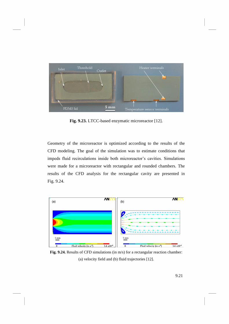
9.21
Fig. 9.23. LTCC-based enzymatic microreactor [12].
Geometry of the microreactor is optimized according to the results of the
CFD modeling. The goal of the simulation was to estimate conditions that
impeds fluid recirculations inside both microreactor’s cavities. Simulations
were made for a microreactor with rectangular and rounded chambers. The
results of the CFD analysis for the rectangular cavity are presented in
Fig. 9.24.
Fig. 9.24. Results of CFD simulations (in m/s) for a rectangular reaction chamber:
(a) velocity field and (b) fluid trajectories [12].
9.21

9.22
As can be seen in Fig. 9.24 in the corners of the rectangular chamber the areas
of fluid recirculations are formed. As a result, an effective pumping out of the
entire volume from the reaction chamber is hindered. Moreover, the fluid
recirculation in the corners makes the removal of all used beads with enzyme
(e.g. for enzyme regeneration) impossible. The results of computations
obtained for a rounded chamber are presented in Fig. 9.25.
Fig. 9.25. Results of CFD simulations (in m/s) for a rounded reaction chamber:
(a) velocity field and (b) fluid trajectories [12].
Fig. 9.26. Calibration curve for an enzymatic microreactor with urease immobilized
onto glass beads.
9.22

9.23
For this version of the microfluidic reactor the areas of fluid recirculation
seem to be eliminated. Calibration curve for an enzymatic microreactor is
shown in Fig. 9.26. The output signal of the microreactor loaded with enzyme
immobilized onto pours glass beads is very high – ca. 2.5 pH units – and
comparable with the output signal reported for silicon-based micro-
reactor [16]. The main features of the presented batch type enzymatic
microreactor are the following: variety of materials for an enzyme support,
simplicity of upload, easy control of enzyme activity and very good long-term
stability.
PCR (Polymerase Chain Reaction) microreactors
The polymerase chain reaction (PCR) is a unique temperature controlled
process, by which the selected DNA fragments can be copied many times. It
is one of if the most important techniques which finds practical application in
genetic identification and gene diagnostics. The PCR reaction is performed
during several temperature cycles. Each cycle consists of three specific
temperatures: separating a double-strand DNA (denaturation, T = 94oC),
attaching of the specific primers to the template (annealing, T = 50 - 60oC)
and extending the primers with chemical enzyme (extension, T = 72oC).
Theoretically, after each cycle, the number of DNA segments duplicates what
gives 2n copies of specific DNA molecules in n steps [13].
The miniaturization of the thermocyclers for a rapid DNA amplification has
been playing a major role to meet the current demands in the field of
molecular biology. The PCR micororeactors, in comparison with classical
laboratory equipment, are characterized by quicker thermal cycling, smaller
reactants volumes and less power consumption. Moreover, there is a
possibility to integrate such miniature thermocycler with an optical detection
system in order to develop a real-time PCR device. There are two main
9.23

9.24
approaches to construct the PCR microreactors: flow-through and
microchamber. The flow-through thermocycler consists of a fluidic channel
which is split into three temperature zones. The temperature of each zone
corresponds to the specific temperature of the PCR cycle. The amplification
of the DNA is performed by pumping the sample through the three
temperature zones of the fluidic channels. An exemplary construction of the
flow-through PCR microreactor is presented in Fig. 9.27.
a) b)
Fig. 9.27. (a) Scheme and (b) photograph of the flow-through PCR microreactor
[14].
It consists of a serpentine channel with different cross-sectional areas in
different temperature zones to ensure adequate residence time of the sample
for denaturation, annealing and extension reaction. Air-gaps made in the PCR
microreactor ensure thermal isolation between the individual reaction zones.
Thick-film heaters are fabricated below each reaction zone. They are made of
AgPd paste using screen-printing method. Simulated temperature profiles
across the central plane of the LTCC-based flow-through PCR microreactor
and experimentally validated infrared image of its surface temperature are
presented in Fig. 9.28.
9.24

9.25
a) b)
Fig. 9.28. (a) Simulated temperature profiles across the central plane and (b)
experimentally validated infrared image of the surface temperature profiles of the
three temperature zones [15].
The microchamber PCR reactor is a device where the DNA sample and other
reagents are held whilst the temperature is changing [16]. The device consists
of a reaction chamber, a thick-film heater, a SMD temperature sensor (Pt 100)
and an optical waveguide integrated in one LTCC structure. Integration of the
optical waveguide enables light excitation of the DNA sample for
fluorescence measurements and optical monitoring of the process. The
microchamber PCR reactor is sealed with a sodium glass plate using the
LTCC-glass bonding technique. The LTCC-based microreactor is depicted in
Fig. 9.29.
Fig. 9.29. Microchamber PCR reactor [16].
9.25
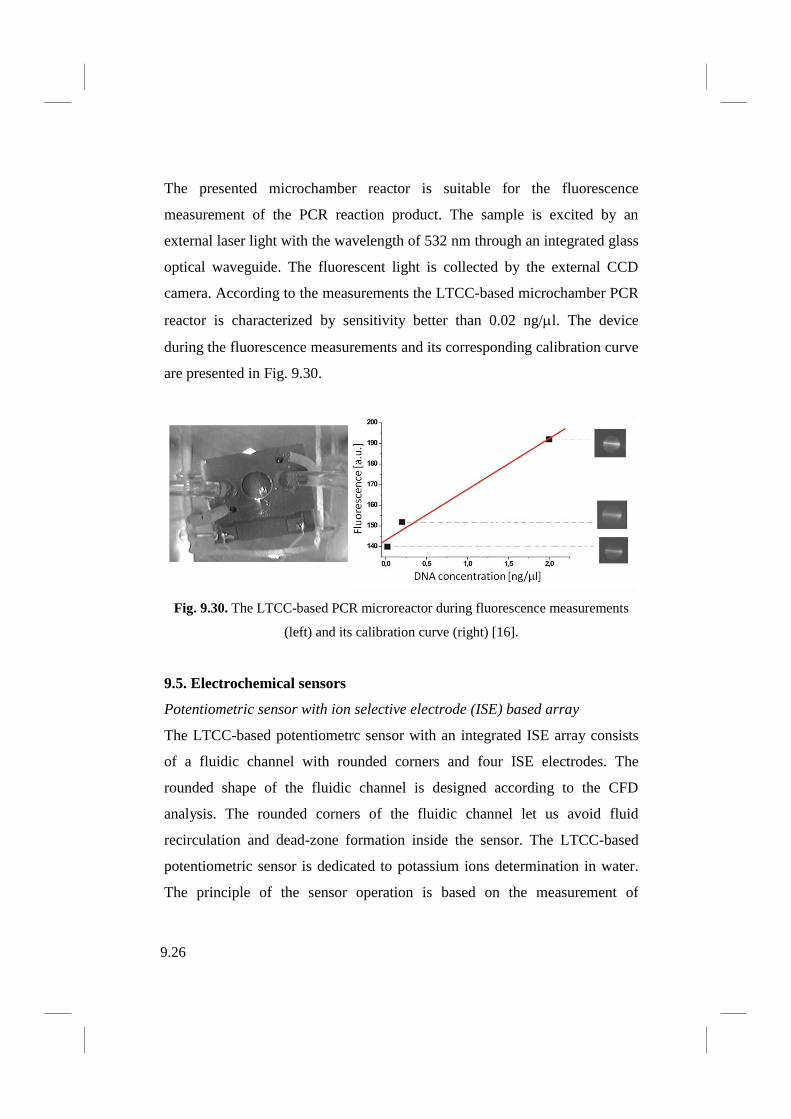
9.26
The presented microchamber reactor is suitable for the fluorescence
measurement of the PCR reaction product. The sample is excited by an
external laser light with the wavelength of 532 nm through an integrated glass
optical waveguide. The fluorescent light is collected by the external CCD
camera. According to the measurements the LTCC-based microchamber PCR
reactor is characterized by sensitivity better than 0.02 ng/l. The device
during the fluorescence measurements and its corresponding calibration curve
are presented in Fig. 9.30.
Fig. 9.30. The LTCC-based PCR microreactor during fluorescence measurements
(left) and its calibration curve (right) [16].
9.5. Electrochemical sensors
Potentiometric sensor with ion selective electrode (ISE) based array
The LTCC-based potentiometrc sensor with an integrated ISE array consists
of a fluidic channel with rounded corners and four ISE electrodes. The
rounded shape of the fluidic channel is designed according to the CFD
analysis. The rounded corners of the fluidic channel let us avoid fluid
recirculation and dead-zone formation inside the sensor. The LTCC-based
potentiometric sensor is dedicated to potassium ions determination in water.
The principle of the sensor operation is based on the measurement of
9.26

9.27
potential of a specific ion in the solution by ISE electrode. This potential is
measured against a stable reference electrode (RE) of constant potential. The
potential difference between the two electrodes depends upon the
concentration of specific ions in solution. The ISE electrodes work on the
basic principle of the galvanic cell (Fig. 9.31).
Fig. 9.31. ISE-based galvanic cell.
By measuring the electric potential generated across a membrane by specific
ions, and comparing it to a reference electrode, a net charge is determined.
The strength of this charge is directly proportional to the concentration of the
selected ions. The potential of the ISE electrode (EISE) depends on the
logarithm of the specific ion concentration, according to the Nikolsky
equation:
ln1
/0
n
j
zn
jijiISE cKcnF
RTEE (9.10)
9.27

9.28
where E0 is the standard electrode potential (V), R is the universal gas
constant (8.314 J·K-1
mol-1
), T is the absolute temperature (K), F is the
Faraday constant (9.648·104 C·mol
-1), Kij is the selectivity coefficient for ion j
of an electrode sensitive to ion i, z is the valence of the primary ion j, n is the
valence of the interfering ion j.
The LTCC-based potentiometric sensor is built of a rounded fluidic channel
and four chambers for ISE electrodes. Each of the chambers consists of three
cavities for an ion-selective membrane, Ag/AgCl electrode and hydrogel
layer. Dimensions of the cavities are equal to 2 mm2, 1.5 mm
2 and 1 mm
2,
respectively. A schematic view of the LTCC-based potentiometrc sensor with
integrated ISE array is illustrated in Fig. 9.32.
Fig. 9.32. Schematic view of the LTCC-based potentiometric sensor.
The real structure of the sensor was manufactured from nine LTCC tapes. The
fluidic channels and cavities were cut out in ceramic layers using Nd-YAG
laser before firing. The ISE-array located inside of the LTCC module was
deposited with use of silver ink by screen printing method. After laser cutting
and screen printing, all ceramic tapes were laminated and co-fired. The real
structure of the LTCC-based potentiometric sensor is presented in Fig. 9.33.
The silver/silver chloride electrodes were made by electrochemical chloriding
of screen printed silver pads in 0.1 M potassium chloride (+1.5 V vs. Pt
electrode, until total decline of the current for at least 15 minutes). After the
chloriding, the electrodes were chemically modified to form an intermediate
9.28

9.29
hygrogel layer and ion selective membrane. The dynamic response of the
sensor for various concentrations of potassium ions and corresponding
calibration curve are presented in Fig. 9.34.
Fig. 9.33. LTCC potentiometric sensor (after chloridization and deposition of
hydrogel and ion selective membrane layers) [17].
Fig.. 9.34. Time responses and the corresponding calibration curve of the LTCC
potentiometric sensor (potassium ions) [17].
PDMS/ceramic module for potentiometric determination of urea
The microfluidic module is fabricated using a hybrid technology which
combines ceramic and polymeric materials. The device is designed for
determination of urea in biological fluids. Detection of the analyte is based on
the hydrolysis reaction of urea catalyzed by urease (9). By measuring
9.29

9.30
concentration of NH4+ ion, which is one of reaction (9) product, it is possible
to determine urea concentration in the test solution. The concentration of
NH4+ ions is determined using potentiometric method. As can be seen in Fig.
9.35, the flow-through detection module is made of three layers: (a) the
ceramic substrate with deposited silver electrodes, (b) the PDMS thin layer
with the holes for ion-selective membranes and (c) the PDMS cover plate
with a microchannel and inlet/outlet holes. The module is based on ceramic
(96% Al2O3) substrate with screen-printed silver electrodes. The NH4+
selective membranes are deposited on the surface of the electrodes.
Fig. 9.35. Scheme of the module for potentiometric determination of urea [18].
Fig. 9.36. Module made of ceramic and PDMS before (left) and after plasma
bonding (right) [18].
9.30

9.31
Enzyme-urease is covalently immobilized onto the membrane surface. The
ceramic substrate is bonded with the PDMS material using microwave
plasma. The flow-through detection module before and after the bonding
process is presented in Fig. 9.36. The dynamic response and corresponding
calibration curve of the module is presented in Fig. 9.37.
Fig.. 9.37. Time responses and the corresponding calibration curve of the module
[18].
Amperometric sensor for continuous glucose monitoring
A flow-through sensor with an integrated microdialysis tube and three thick-
film electrodes for amperometric detection fabricated using the LTCC
technology is illustrated in Fig. 9.38. This microsystem is destined for
continuous monitoring of various (bio)chemical compounds (e.g. glucose,
lactate, glutamate). The principle of its operations is based on the size
selective diffusion of the glucose. The glucose diffuses from the test sample
through the walls of the semi-permeable dialysis tube to the microreaction
cell. The microreactor is filled with the buffer solution containing free
enzyme – glucose oxidase (GOx).
9.31

9.32
Fig. 9.38. Construction of the amperometric glucose sensor [19].
In the presence of the GOx the glucose is electro-oxidized on the surface of
the working electrode and gluconolactone and hydrogen peroxide is
produced:
2222cos OHtonegluconolacOHOeglu GOx (9.11)
One of the reaction products is a hydrogen peroxide which is detected
amperometrically during its oxidation at the surface of the working electrode:
eHOOH 22222 (9.12)
The current resulting from reaction (12) is a measurand as it is proportional to
the glucose concentration in the sample. The amperometric glucose sensor is
made of ten LTCC layers. The openings for the microreaction cell, the
channel for the microdialysis tube and the electrode terminals are made with a
Nd:YAG laser. Platinum paste is used for construction of the working and
counter electrodes while silver paste is used for the reference electrode. The
LTCC-based amperometric sensor’s reaction cell with a fixed microdialysis
9.32

9.33
tube is presented in Fig. 9.39. The dynamic response and corresponding
calibration curve of the sensor are presented in Fig. 9.40. A linear response of
the LTCC-based amperometric sensor to glucose was up to 13 mM. The
presented ceramic sensor has about ten times higher sensitivity (ca.
135 nA/mM) in comparison with a similar construction of sensor made in
silicon (ca. 16 nA/mM) [19].
Fig. 9.39. Reaction cell with attached microdialysis tube [19].
Fig. 9.40. (a) Dynamic response and (b) calibration curve of the LTCC glucose
sensor [20].
a) b)
9.33

9.34
Electrochemical sensor for heavy metal determination in biomedical and
environmental fluids
The LTCC-based manifold for heavy metal detection using anodic stripping
voltammetry is presented in Fig. 9.41. The anodic stripping voltammetry is an
electrochemical method for quantitative determination of specific ions in the
test solution. The detected analyte is firstly electroplated on the surface of the
working electrode (WE) and then oxidized on the electrode during the
stripping step. In the electroplating step the WE potential is held at a
relatively low level. The potential should be low enough to reduce the analyte
deposit on the electrode. During the stripping step the potential is rising what
results in an oxidation of the analyte. As a result of the oxidation the analyte
gives off the electrons which can be measured as a current. The sensor
structure is made of seven LTCC. It consists of two fluidic inlets,
microchannels, a spiral passive mixer (when a reagent addition is necessary),
a measuring cavity, an electrode array and a fluidic outlet.
a) b)
Fig. 9.41. LTCC-based electrochemical sensor: (a) layers for device, (b) fabricated
structure [21].
The electrode array for electrochemical measurements is fabricated using
thick-film screen printable pastes. The sensor array is composed of
9.34

9.35
silver/silver chloride reference electrode, a gold counter electrode and two
gold working electrodes. The reference electrode is obtained by silver electro-
deposition in a solution of AgNO3 and NH4OH. The experimental results of
square-wave anodic stripping voltammetry obtained for increasing
concentrations of copper and mercury are presented in Fig. 9.42.
Fig. 9.42. Square-wave stripping responses for increasing concentrations of
copper and mercury [21].
9.6. Optical sensors
LTCC-based microfluidic sensor for absorbance measurement
The principle of the sensor operation is based on light absorption by the
medium (analyte) which flows in an analytical microchannel between two
optical fibers. The changes in light intensity which approaches the
photodetector are related to the changes in the analyte concentration. A light
absorbance according to Lambert-Beer’s law is defined as follows:
9.35

9.36
lcI
IA o
log (9.13)
where: Io and I are intensities of the light, c is the molar concentration, is the
molar absorptivity (cm-1
M-1
) and l is the optical path length. So it can be
noticed that for the same conditions of measurement (the same optical path
lengths and molar absorptivity of measured solution) the absorbance is
proportional to the concentration of considered chemical in a particular
solution. The LTCC microfluidic sensor for absorbance measurements
presented in Fig. 9.43 consists of fluidic channels, channels for optical fibers
and two polymeric optical fibers. The light emitting diode (LED) is applied as
a light source and photodiode coupled with an amplifier and color filter is
applied as a light detector.
a)
b)
Fig. 9.43. LTCC-based microfluidic optical sensor: (a) schematic view and (b)
photograph [22].
The measured output signal is proportional to the light intensity coming to the
light detector device. So it is possible to measure the light absorbance versus
the concentration of analyte utilizing the following formula:
9.36

9.37
)(log
)(log)(
cU
U
cI
IcA oo
(9.14)
where Uo is the output voltage for pure water and U(c) is the voltage level
related to concentration c. The results of the absorbance measurements for the
LTCC sensor are given in Fig. 9.44.
Fig. 9.44. Light absorbance vs. concentration of Sunset Yellow dye
measured at wavelength = 468 nm [22].
LTCC-based fluorescent sensor
The LTCC technology is applied to fabrication of a fluorescent detection
module. The principle of the presented device operation is based on
fluorescence activated cell detection. The LTCC-based fluorescent sensor
presented in Fig. 9.45 consists of a microfluidic chamber, two polymeric fibre
optics, a miniature light source (UV light emitting diode) and a photodetector
(photodiode integrated with an amplifier and a color filter in one CMOS
structure).
9.37

9.38
Fig. 9.45. LTCC-based fluorescent sensor [23].
Fig. 9.46. Response of the LTCC-based fluorescent sensor for various concentrations
of Escherichia coli and Saccharomyces cerevisiae cells [23].
The sample is illuminated by UV light which is transmitted via the input
optical fibre to the detection chamber. As a result of the light excitation the
9.38
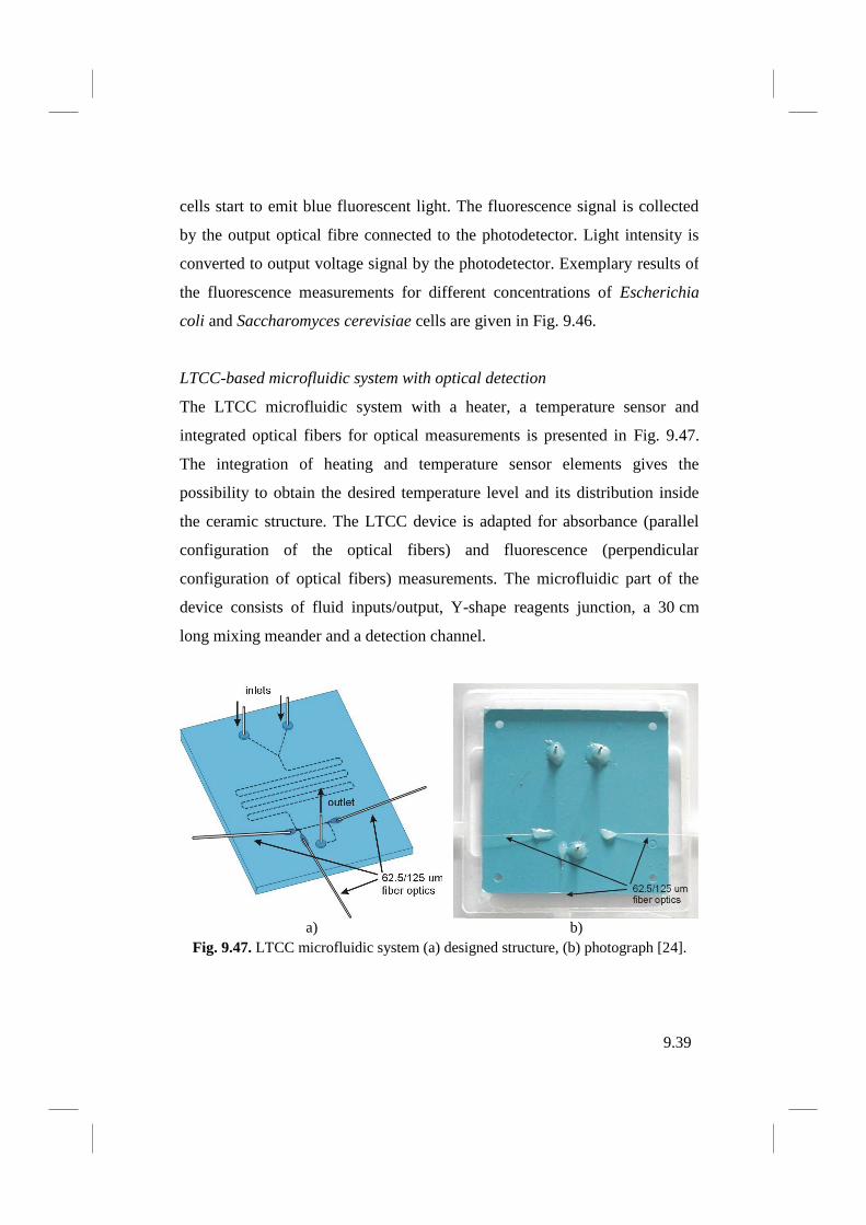
9.39
cells start to emit blue fluorescent light. The fluorescence signal is collected
by the output optical fibre connected to the photodetector. Light intensity is
converted to output voltage signal by the photodetector. Exemplary results of
the fluorescence measurements for different concentrations of Escherichia
coli and Saccharomyces cerevisiae cells are given in Fig. 9.46.
LTCC-based microfluidic system with optical detection
The LTCC microfluidic system with a heater, a temperature sensor and
integrated optical fibers for optical measurements is presented in Fig. 9.47.
The integration of heating and temperature sensor elements gives the
possibility to obtain the desired temperature level and its distribution inside
the ceramic structure. The LTCC device is adapted for absorbance (parallel
configuration of the optical fibers) and fluorescence (perpendicular
configuration of optical fibers) measurements. The microfluidic part of the
device consists of fluid inputs/output, Y-shape reagents junction, a 30 cm
long mixing meander and a detection channel.
a) b)
Fig. 9.47. LTCC microfluidic system (a) designed structure, (b) photograph [24].
9.39
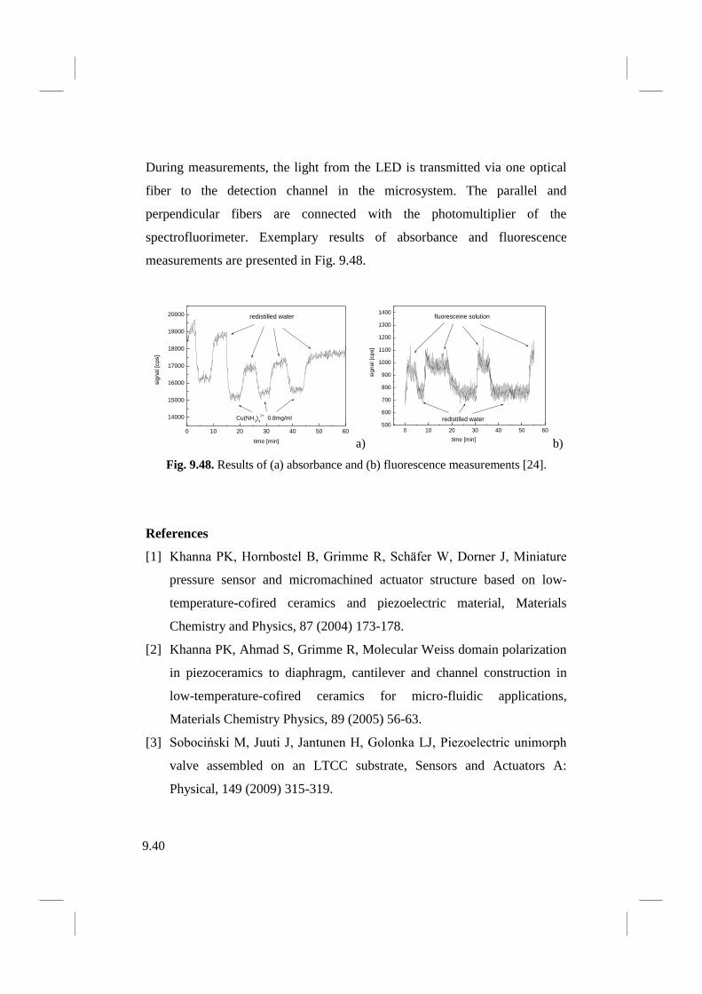
9.40
During measurements, the light from the LED is transmitted via one optical
fiber to the detection channel in the microsystem. The parallel and
perpendicular fibers are connected with the photomultiplier of the
spectrofluorimeter. Exemplary results of absorbance and fluorescence
measurements are presented in Fig. 9.48.
a) b)
Fig. 9.48. Results of (a) absorbance and (b) fluorescence measurements [24].
References
[1] Khanna PK, Hornbostel B, Grimme R, Schäfer W, Dorner J, Miniature
pressure sensor and micromachined actuator structure based on low-
temperature-cofired ceramics and piezoelectric material, Materials
Chemistry and Physics, 87 (2004) 173-178.
[2] Khanna PK, Ahmad S, Grimme R, Molecular Weiss domain polarization
in piezoceramics to diaphragm, cantilever and channel construction in
low-temperature-cofired ceramics for micro-fluidic applications,
Materials Chemistry Physics, 89 (2005) 56-63.
[3] Sobociński M, Juuti J, Jantunen H, Golonka LJ, Piezoelectric unimorph
valve assembled on an LTCC substrate, Sensors and Actuators A:
Physical, 149 (2009) 315-319.
0 10 20 30 40 50 60
14000
15000
16000
17000
18000
19000
20000 redistilled water
Cu(NH3)
4
2+ 0.8mg/ml
sig
na
l [c
ps]
time [min]
0 10 20 30 40 50 60500
600
700
800
900
1000
1100
1200
1300
1400
redistilled water
fluoresceine solution
time [min]
sig
na
l [c
ps]
9.40

9.41
[4] Huang et al., Proc. 6th International Conference and Ceramic
Microsystems Technologies, 2010.
[5] Sethu P, Mastrangel CH, Polyethylene glycol (PEG)-based actuator for
nozzle-diffuser pumps in plastic microfluidic systems, Sensors and
Actuators A: Physical, 104 (2003) 283-289.
[6] Gongora-Rubio MR, Espinoza-Vallejos P, Sola-Laguna L, Santiago-
Avilés JJ, Overview of low temperature co-fired ceramics tape
technology for meso-system technology (MsST), Sensors and Actuators
A: Physical, 89 (2001) 222-241.
[7] da Cunha MR, Saul CK, Gongora-Rubio MR, Numerical and
experimental analysis of microfluidic diode manufactured in LTCC
technology, Proc. International Conference IBERSENSOR, 2006, 1-5.
[8] Nguyen NT, Wu Z, Micromixers – a review, Journal of Micromechanics
and Microengineering, 15 (2005) R1-R16.
[9] Bau HH, Zhong J, Yi M, A minute magneto hydro dynamic (MHD)
mixer, Sensors and Actuators B: Chemical, 79 (2001) 207-215.
[10] Yi M, Bau HH, The kinematics of bend-induced mixing in micro-
conduits, International Journal of Heat and Fluid Flow, 24 (2003) 645-
656.
[11] Malecha K, Golonka LJ, Bałdyga J, Jasińska M, Sobieszuk P, Serpentine
microfluidic mixer made in LTCC, Sensors and Actuators B: Chemical,
143 (2009) 400-413.
[12] Malecha K, Pijanowska DG, Golonka LJ, Torbicz W, LTCC
microreactor for urea determination in biological fluids, Sensors and
Actuators B: Chemical, 141 (2009) 301-308.
[13] Budniewski K, Golonka LJ, Zawada T, Roguszczak H, Dobosz T,
Jonkisz A, Design and FEM analysis of novel microchamber PCR device
9.41

9.42
fabricated in LTCC technology, Proc. 28th
International Conference of
IMAPS Poland Chapter, Wrocław (Poland), September 2004, 191-194.
[14] Sadler DJ, Changrani R, Roberts P, Chou CF, Zanhausern F, Thermal
management of BioMEMS: temperature control for ceramic-based PCR
and DNA detection devices, IEEE Transactions on Components and
Packaging Technologies, 26 (2003) 309-316.
[15] Chou CF, Changrani R, Roberts P, Sadler D, Burdon J, Zenhausen F, Lin
S, Mulholland A, Swami N, Terbrueggen R, A miniaturized cyclic PCR
device – modeling and experiments, Microelectronic Engineering, 61-62
(2002) 921-925.
[16] Bembnowicz P, Małodobra M, Kubicki W, Szczepańska P, Górecka-
Drzazga A, Dziuban J, Jonkisz A, Karpiewska A, Dobosz T, Golonka LJ,
Preliminary studies on LTCC based PCR microreactor, Sensors and
Actuators B: Chemical, 150 (2010) 715-721.
[17] Malecha K, Pijanowska DG, Dawgul M, Golonka LJ, Torbicz W, LTCC
fluidic potentiometric detector, Proc. 31st IEEE International Spring
Seminar on Electronic Technology, Budapest (Hungary) , May 2008,
498-503.
[18] Grabowska I, Ksok E, Wyżkiewicz I, Chudy M, Miniaturized module
with biosensors for potentiometric determination of urea, Microchimica
Acta, 164 (2009) 299-305.
[19] Malecha K, Pijanowska DG, Golonka LJ, Kurek P, Low temperature co-
fired ceramic (LTCC)-based biosensor for continuous glucose
monitoring, Sensors and Actuators B: Chemical, (2011)
doi:10.1016/j.snb.2011.01.002.
[20] Malecha K, Pijanowska DG, Golonka LJ, Kurek P, LTCC flow-through
amperometric sensor for glucose determination, Proc. 5th
IMAPS/ACerS
9.42

9.43
International Ceramic Interconnect and Ceramic Microsystem
Technologies, Denver (USA), April 2009, 157-162.
[21] Gongora-Rubio MR, Fontes MBA, da Rocha ZM, Richter EM, Angnes
L, LTCC manifold for heavy metal detection system in biomedical and
environmental fluids, Sensors and Actuators B: Chemical, 103 (2004)
468-473.
[22] Malecha K, Zawada T, Golonka LJ, LTCC based microfluidic optical
detector, Proc. 28th
IEEE International Spring Seminar on Electronic
Technology, Wiener Neustadt (Austria), May 2005, pp. 347-351.
[23] Malecha K, Czok M, Hetnar A, Pawlik A, Sztajer H, Golonka LJ, Micro
ceramic cell analyzer (MCCA) - preliminary results, Proc. 34th
International Conference and Exhibition IMAPS-CPMT Poland,
Wrocław (Poland), September 2010.
[24] Golonka LJ, Roguszczak H, Zawada T, Radojewski J, Grabowska I,
Chudy M, Dybko A, Brzózka Z, Stadnik D, LTCC based microfluidic
system with optical detection, Sensors and Actuators B: Chemical, 111-
112 (2005) 396-402.
9.43