Embed Size (px)
Citation preview
Jurnal Kejuruteraan SI 1(3) 2018: 15-22http://dx.doi.org/10.17576/jkukm-2018-si1(3)-03
P-type Cu2ZnSnS4 as Multifunctional Material for Photovoltaic and ThermoelectricApplication: Theoretical Investigation
(Cu2ZnSnS4 Jenis-p sebagai Bahan Pelbagai Fungsi untuk Aplikasi Photovolta dan Termoelektrik: Siasatan Teori)
Hassan Ahmouma,*, Mourad Boughraraa, Mohamed Kerouada
a Faculty of Sciences, University Moulay Ismail, Morocco
Puvaneswaran Chelvanathanb, Kamaruzzaman Sopianb, Mohd Sukor Su’aitb* bSolar Energy Research Institute (SERI), Universiti Kebangsaan Malaysia, Malaysia
Lee Tian Khoonc*
c Fuel Cell Institute, Universiti Kebangsaan Malaysia, Bangi, Malaysia
Baohai Jiad, Guojian Lid
d Key Laboratory of Electromagnetic Processing of Materials (Ministry of Education), Northeastern University, China
ABSTRACT
In this work, a detailed information about physical properties of Cu2ZnSnS4 stannite phase by first principles calculation has been presented. Using density functional theory based on the generalized gradient approximation GGA, the structural properties such as lattice parameters and bulk modulus has been determined. In addition, structure electronic and partial density of state to characterize the electronic properties was also calculated. For the optical properties investigation, the absorption coefficient and the efficiency of energy conversion has been calculated. Finally, we have investigated on thermoelectric properties such as electrical conductivity, Seebeck coefficient, thermal conductivity and figure of merit to evaluate the potential of this material in different applications. From our results presented herein, we conclude that this material can be considered potential multifunctional material for thermoelectric and photovoltaic applications.
Keywords: Cu2ZnSnS4; first principles study; material modeling, photovoltaic; thermoelectric
ABSTRAK
Dalam kajian ini, sifat fizikal Cu2ZnSnS4 berfasa stanit telah dijalankan dengan menggunakan pengiraan prinsip pertama telah dipersembahkan dengan terperinci. Dengan menggunakan teori fungsi kepadatan (DFT) yang berdasarkan kepada anggaran kecerunan umum (GGA), sifat struktur seperti tenaga kekisi dan modulus pukal Cu2ZnSnS4 telah ditentukan. Selain itu, sifat elektronik Cu2ZnSnS4 ini ditentukan melalui pengiraan terhadap struktur elektronik dan ketumpatan keadaan separa (partial density of state). Sifat optik Cu2ZnSnS4 juga telah disiasat melalui pengiraan terhadap pekali serapan dan kecekapan penukaran tenaga. Akhir sekali, kami juga menyiasat pekali Seebeck, kekonduksian terma dan angka merit untuk mencungkil potensi bahan ini dalam aplikasi lain. Daripada hasil kajian yang telah diperolehi, kami boleh menyimpulkan bahawa bahan ini mempunyai potensi dan peranan sebagai bahan kepelbagaian fungsi dalam aplikasi terma elektrik dan fotovoltaik.
Kata kunci: Cu2ZnSnS4; kajian prinsip pertama; pemodalan bahan, fotovoltaik; terma elektrik
INTRODUCTION
Solar energy has been considered one of the most feasible solution to compensate the energy consumed on the whole planet by harvesting the sunlight and converting the solar energy to electricity by using the photovoltaic technology. Moreover, hybridization of photovoltaic (PV) and thermoelectric (TE) technology device has long been considered ideal for efficient harnessing solar energy. The TE is technology which allow its material to transfer a gradient thermal energy and converting it to electrical energy
(Mohamed et al. 2016). The combination of PV-TE technology is very important as it can utilize the full spectrum of solar energy via lossless coupling between PV and TE device through the collection of waste energy from thermalization and transmission losses from PV device, which subsequently, provides the maximum (or near maximum) power output (Park et al. 2013).
In terms of material used, chalcogenide alloys such as Cu(In,Ga)Se2 (CIGS), Cu2ZnSnS4 (CZTS) and GaAs are interesting to be studied (Sakib & Ahad 2018). Cu(In,Ga)Se2 (CIGS) is already integrated in the commercial solar cell
JK 30 SI1(3) Bab 3.indd 15 12/4/2018 2:02:41 PM
16
because of its high conversion energy which has already achieved efficiency of 20.8% (Jackson et al. 2014). While Na0.2Pb0.8Te is the most used material in the thermoelectric device and it has higher figure of merit around 1.74 at 774 K (Wang et al. 2013). Howbeit, the high cost and toxicity of these elements are the main concerns and responsible for the high price of these conversion materials. In order to meet the challenges of low cost PV and TE devices, the need to explore other materials and alternatives are inevitable. For this reason, we have investigated on the Cu2ZnSnS4 (CZTS) because of various advantages such as earth abundant and environmentally friendly component elements (nontoxic elements Cu, Zn, S and Sn), optimal direct band gap (1.5 eV), high absorption coefficients 105 cm-1 (Ricardo et al. 2013) and it is a semiconductor with p-type conductivity (Olgar et al. 2017). Consequently, CZTS has already found in several technologies such as photovoltaic (Mahajan et al. 2018), thermoelectric (Kumar et al. 2018) and photocatalysis (Hou et al. 2014). In fact, CZTS is considered one of the most explored material in the recent years, by experimental and computational methods. For example, Reshak et al. (2014) have investigated on the electronic and optical properties of kesterite CZTS by mean of density functional theory (DFT) and they have showed that this material can be used as an absorption material because of the value of band gap. On the other hand, Liu et al. (2009) have investigated on the thermoelectric properties of kestrite phase of Cu2ZnSnQ4 (Q = S, Se) and they have showed that CZTS can be used as a p-type thermoelectric material. As we know, CZTS material generally exists in two types of crystal structures, i.e, kesterite and stannite with space group of I-4 and I-4 2m, respectively (Quennet et al. 2017). Most of the DFT studies have been focused on the kesterite structure. However, many researchers, by experimental, have synthesis the CZTS with the presence of two phases (stannite and kesterite). While, other researchers have synthesis CZTS with pure stannite phase. The knowledge of the physical properties of stannite phase by DFT is obligatory, especially to the best of our knowledge, there are no papers published on thermoelectric study related to stannite CZTS. For this reason, in this paper, we explored the crystalline structure, electronic, electrical, optical and thermoelectric properties of stannite CZTS. By using the first principal approach, we calculated the properties of stannite CZTS. The relationship between photovoltaic and thermoelectric performance will be discussed in this paper, and a possible explanation for previous experimental observations will be provided. This work should and will help to deepen understand on stannite CZTS compound.
METHODOLOGY
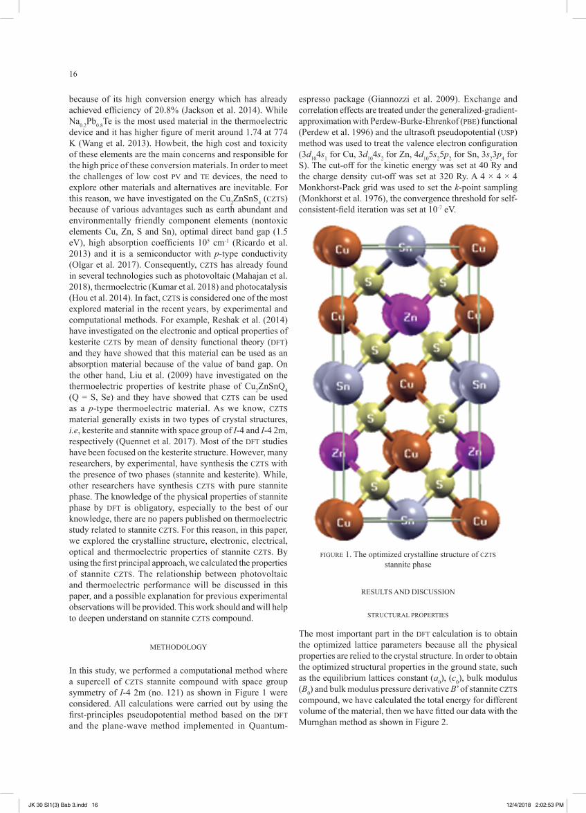
In this study, we performed a computational method where a supercell of CZTS stannite compound with space group symmetry of I-4 2m (no. 121) as shown in Figure 1 were considered. All calculations were carried out by using the first-principles pseudopotential method based on the DFT and the plane-wave method implemented in Quantum-
espresso package (Giannozzi et al. 2009). Exchange and correlation effects are treated under the generalized-gradient-approximation with Perdew-Burke-Ehrenkof (PBE) functional (Perdew et al. 1996) and the ultrasoft pseudopotential (USP) method was used to treat the valence electron configuration (3d104s1 for Cu, 3d104s2 for Zn, 4d105s25p2 for Sn, 3s23p4 for S). The cut-off for the kinetic energy was set at 40 Ry and the charge density cut-off was set at 320 Ry. A 4 × 4 × 4 Monkhorst-Pack grid was used to set the k-point sampling (Monkhorst et al. 1976), the convergence threshold for self-consistent-field iteration was set at 10-7 eV.
FIGURE 1. The optimized crystalline structure of CZTS stannite phase
RESULTS AND DISCUSSION
STRUCTURAL PROPERTIES
The most important part in the DFT calculation is to obtain the optimized lattice parameters because all the physical properties are relied to the crystal structure. In order to obtain the optimized structural properties in the ground state, such as the equilibrium lattices constant (a0), (c0), bulk modulus (B0) and bulk modulus pressure derivative B’ of stannite CZTS compound, we have calculated the total energy for different volume of the material, then we have fitted our data with the Murnghan method as shown in Figure 2.
JK 30 SI1(3) Bab 3.indd 16 12/4/2018 2:02:53 PM
17
According to the results, the lattice parameters of pure CZTS are a0 = 5.50 c0 = 10.98 Å, and this result are close to the theoretical value found by Zhao et al. (2017) which are a0 = 5.48 c0 = 10.96 Å. Whereas, the experimental results show that CZTS possessed of a0 = 5.449 c0 = 10.757 Å lattice parameters (Gusain et al. 2014). The differences between the DFT results with the experimental results are that the method generalized gradient approximation (GGA) that we have used for calculation is always considering of overestimated the value of the equilibrium lattice parameter. Finally, our value of the bulk modulus is in excellent agreement with the values obtained by Zhao et al. (2017) which is 64.39 GPa. From these results, we conclude that our method of calculations is feasible and reliable.
ELECTRONIC PROPERTIES
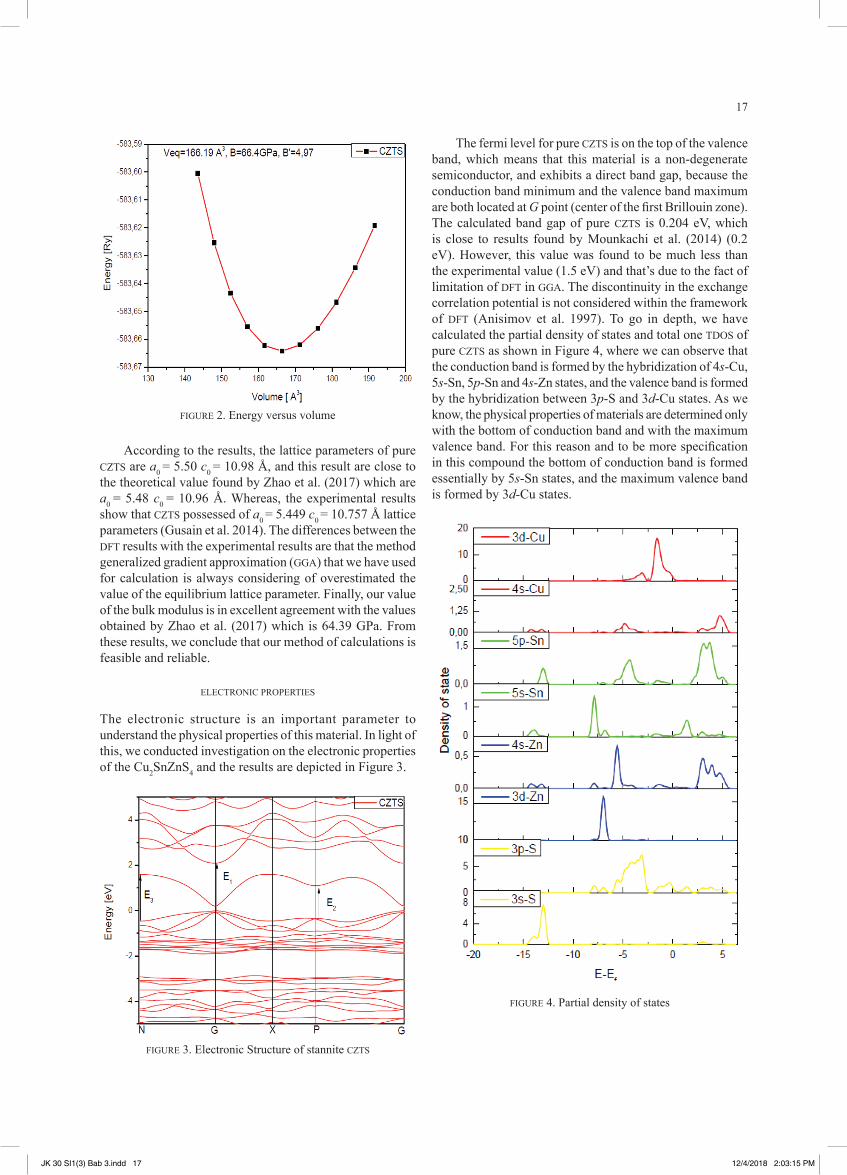
The electronic structure is an important parameter to understand the physical properties of this material. In light of this, we conducted investigation on the electronic properties of the Cu2SnZnS4 and the results are depicted in Figure 3.
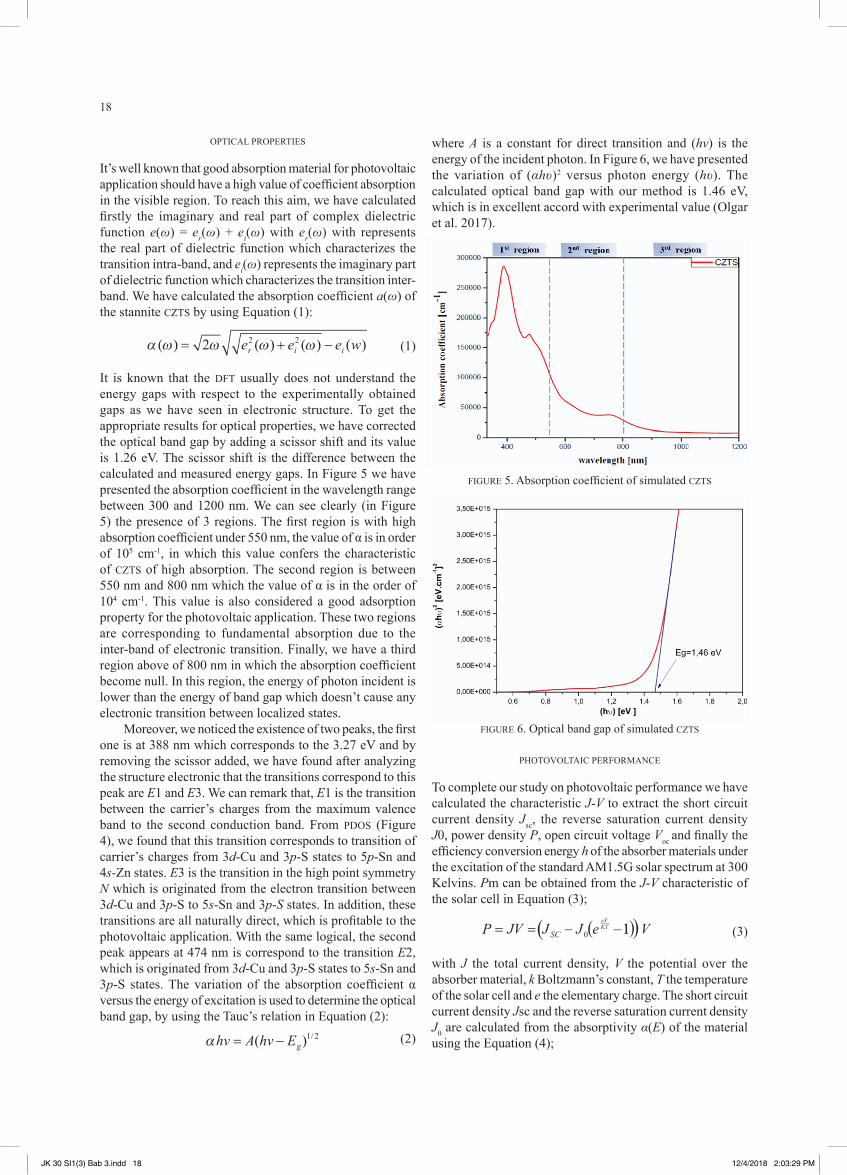
The fermi level for pure CZTS is on the top of the valence band, which means that this material is a non-degenerate semiconductor, and exhibits a direct band gap, because the conduction band minimum and the valence band maximum are both located at G point (center of the first Brillouin zone). The calculated band gap of pure CZTS is 0.204 eV, which is close to results found by Mounkachi et al. (2014) (0.2 eV). However, this value was found to be much less than the experimental value (1.5 eV) and that’s due to the fact of limitation of DFT in GGA. The discontinuity in the exchange correlation potential is not considered within the framework of DFT (Anisimov et al. 1997). To go in depth, we have calculated the partial density of states and total one TDOS of pure CZTS as shown in Figure 4, where we can observe that the conduction band is formed by the hybridization of 4s-Cu, 5s-Sn, 5p-Sn and 4s-Zn states, and the valence band is formed by the hybridization between 3p-S and 3d-Cu states. As we know, the physical properties of materials are determined only with the bottom of conduction band and with the maximum valence band. For this reason and to be more specification in this compound the bottom of conduction band is formed essentially by 5s-Sn states, and the maximum valence band is formed by 3d-Cu states.
FIGURE 2. Energy versus volume
FIGURE 3. Electronic Structure of stannite CZTS
FIGURE 4. Partial density of states
JK 30 SI1(3) Bab 3.indd 17 12/4/2018 2:03:15 PM
18
OPTICAL PROPERTIES
It’s well known that good absorption material for photovoltaic application should have a high value of coefficient absorption in the visible region. To reach this aim, we have calculated firstly the imaginary and real part of complex dielectric function e(ω) = er(ω) + ei(ω) with er(ω) with represents the real part of dielectric function which characterizes the transition intra-band, and ei(ω) represents the imaginary part of dielectric function which characterizes the transition inter-band. We have calculated the absorption coefficient a(ω) of the stannite CZTS by using Equation (1):
α ω ω ω ω
α
( ) ( ) ( ) ( )
( ) /
= + −
= −
= = − −
2 2 2
1 2
0
e e e w
hv A hv E
P JV J J e
r i i
g
SC
eVKT 11
1 2
0
0 0
V
a E e
J e a E I dE
Je
fra E I dE
ZT
E L
SC sun
bb
( )
( )
( )
( )= −
=
=
=
−
∞
∞
∫
∫
α
π
σσ
η
S T
K
T T ZT
ZTTT
h c
c
h
2
1 1
1=
− + −
+ +
(1)
It is known that the DFT usually does not understand the energy gaps with respect to the experimentally obtained gaps as we have seen in electronic structure. To get the appropriate results for optical properties, we have corrected the optical band gap by adding a scissor shift and its value is 1.26 eV. The scissor shift is the difference between the calculated and measured energy gaps. In Figure 5 we have presented the absorption coefficient in the wavelength range between 300 and 1200 nm. We can see clearly (in Figure 5) the presence of 3 regions. The first region is with high absorption coefficient under 550 nm, the value of α is in order of 105 cm-1, in which this value confers the characteristic of CZTS of high absorption. The second region is between 550 nm and 800 nm which the value of α is in the order of 104 cm-1. This value is also considered a good adsorption property for the photovoltaic application. These two regions are corresponding to fundamental absorption due to the inter-band of electronic transition. Finally, we have a third region above of 800 nm in which the absorption coefficient become null. In this region, the energy of photon incident is lower than the energy of band gap which doesn’t cause any electronic transition between localized states.
Moreover, we noticed the existence of two peaks, the first one is at 388 nm which corresponds to the 3.27 eV and by removing the scissor added, we have found after analyzing the structure electronic that the transitions correspond to this peak are E1 and E3. We can remark that, E1 is the transition between the carrier’s charges from the maximum valence band to the second conduction band. From PDOS (Figure 4), we found that this transition corresponds to transition of carrier’s charges from 3d-Cu and 3p-S states to 5p-Sn and 4s-Zn states. E3 is the transition in the high point symmetry N which is originated from the electron transition between 3d-Cu and 3p-S to 5s-Sn and 3p-S states. In addition, these transitions are all naturally direct, which is profitable to the photovoltaic application. With the same logical, the second peak appears at 474 nm is correspond to the transition E2, which is originated from 3d-Cu and 3p-S states to 5s-Sn and 3p-S states. The variation of the absorption coefficient α versus the energy of excitation is used to determine the optical band gap, by using the Tauc’s relation in Equation (2):
α ω ω ω ω
α
( ) ( ) ( ) ( )
( ) /
= + −
= −
= = − −
2 2 2
1 2
0
e e e w
hv A hv E
P JV J J e
r i i
g
SC
eVKT 11
1 2
0
0 0
V
a E e
J e a E I dE
Je
fra E I dE
ZT
E L
SC sun
bb
( )
( )
( )
( )= −
=
=
=
−
∞
∞
∫
∫
α
π
σσ
η
S T
K
T T ZT
ZTTT
h c
c
h
2
1 1
1=
− + −
+ +
(2)
where A is a constant for direct transition and (hv) is the energy of the incident photon. In Figure 6, we have presented the variation of (αhυ)2 versus photon energy (hυ). The calculated optical band gap with our method is 1.46 eV, which is in excellent accord with experimental value (Olgar et al. 2017).
FIGURE 5. Absorption coefficient of simulated CZTS
FIGURE 6. Optical band gap of simulated CZTS
PHOTOVOLTAIC PERFORMANCE
To complete our study on photovoltaic performance we have calculated the characteristic J-V to extract the short circuit current density Jsc, the reverse saturation current density J0, power density P, open circuit voltage Voc and finally the efficiency conversion energy h of the absorber materials under the excitation of the standard AM1.5G solar spectrum at 300 Kelvins. Pm can be obtained from the J-V characteristic of the solar cell in Equation (3);
α ω ω ω ω
α
( ) ( ) ( ) ( )
( ) /
= + −
= −
= = − −
2 2 2
1 2
0
e e e w
hv A hv E
P JV J J e
r i i
g
SC
eVKT 11
1 2
0
0 0
V
a E e
J e a E I dE
Je
fra E I dE
ZT
E L
SC sun
bb
( )
( )
( )
( )= −
=
=
=
−
∞
∞
∫
∫
α
π
σσ
η
S T
K
T T ZT
ZTTT
h c
c
h
2
1 1
1=
− + −
+ +
( (( (
(3)
with J the total current density, V the potential over the absorber material, k Boltzmann’s constant, T the temperature of the solar cell and e the elementary charge. The short circuit current density Jsc and the reverse saturation current density J0 are calculated from the absorptivity α(E) of the material using the Equation (4);
JK 30 SI1(3) Bab 3.indd 18 12/4/2018 2:03:29 PM
19
α ω ω ω ω
α
( ) ( ) ( ) ( )
( ) /
= + −
= −
= = − −
2 2 2
1 2
0
e e e w
hv A hv E
P JV J J e
r i i
g
SC
eVKT 11
1 2
0
0 0
V
a E e
J e a E I dE
Je
fra E I dE
ZT
E L
SC sun
bb
( )
( )
( )
( )= −
=
=
=
−
∞
∞
∫
∫
α
π
σσ
η
S T
K
T T ZT
ZTTT
h c
c
h
2
1 1
1=
− + −
+ +
(4)
where α(E) the absorptivity for an absorber material, α(E) is the absorption coefficient and L is the thickness of the material with a reflecting back surface. The short circuit current density Jsc and the reverse saturation current density J0 can be calculated by using Equation (5) and (6);
α ω ω ω ω
α
( ) ( ) ( ) ( )
( ) /
= + −
= −
= = − −
2 2 2
1 2
0
e e e w
hv A hv E
P JV J J e
r i i
g
SC
eVKT 11
1 2
0
0 0
V
a E e
J e a E I dE
Je
fra E I dE
ZT
E L
SC sun
bb
( )
( )
( )
( )= −
=
=
=
−
∞
∞
∫
∫
α
π
σσ
η
S T
K
T T ZT
ZTTT
h c
c
h
2
1 1
1=
− + −
+ +
(5)
α ω ω ω ω
α
( ) ( ) ( ) ( )
( ) /
= + −
= −
= = − −
2 2 2
1 2
0
e e e w
hv A hv E
P JV J J e
r i i
g
SC
eVKT 11
1 2
0
0 0
V
a E e
J e a E I dE
Je
fra E I dE
ZT
E L
SC sun
bb
( )
( )
( )
( )= −
=
=
=
−
∞
∞
∫
∫
α
π
σσ
η
S T
K
T T ZT
ZTTT
h c
c
h
2
1 1
1=
− + −
+ +
(6)
where Isun and Ibb are AM1.5G solar spectrum and the black body spectrum for room temperature respectively. The fraction of radiative recombination is chosen to be fr = 1, because CZTS material have the characteristic of direct band gap.
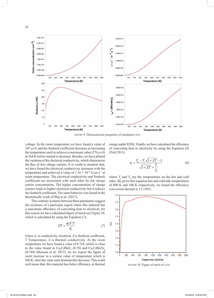
merit, by using Boltztrap code (Madsen et al. 2016) which is based on the semiclassical Boltztrap transport theory and the rigid band approach. However, for the relaxation time which is not obtained by using Boltztrap code, we supposed that the relaxation time is independent with energy. These approaches have been demonstrated to be a reasonably good approximation of several bulk thermoelectric materials (Hammi et al. 2017). In generally, the heat conduction in materials is due by phonon (lattice vibration) and electrons. At low temperature the phonon lattice thermal conductivity is the most dominant, and for higher temperature the electronic thermal conductivity becomes predominant. Therefore, the Boltztrap code calculate only the electronic thermal conductivity.
The thermal conductivity for stannite CZTS is shown in Figure 9, which increases as the temperature increasing and that's because the increasing of temperature lead to increase the probability interaction between electron-electron, and that’s is the origin of the increasing of thermal conductivity versus temperature. Also, we show the variation of the charges carriers as function of the temperature. As first remark, we observed that the concentration of charges carriers increase with the increasing of the temperature which provide the characteristic of semiconductor behavior, and the carriers concentration in the room temperature was found to be 8.89 × 1019 cm–3 which is close to the experimental measurement 2.6 × 1019 cm–3 found by Fernandes et al. (2011), the difference between our calculation and the experimental measurement is that in the experimental there’s the presence of defect which we did not considered in our study. To determine the nature of these carriers charges we have calculated the Seebeck coefficient. We remark that the Seebeck coefficient is positive which indicates that the charges carriers are holes, which mean that the nature of conduction in stannite CZTS is p-type conduction. A good thermoelectric material is the one which has a higher value of Seebeck coefficient and figure of merit. By definition the Seebeck coefficient indicates the capability of a material to converse a gradient temperature to
FIGURE 7. J-V characteristic of CZTS
In order to determine the optimized thickness where the material absorbs the totally incident photon, we have calculated the short circuit current density Jsc as a function of thickness, as shown in Figure 8. It is clearly shown that the short circuit current density Jsc of stannite CZTS become invariant with the increase of thickness of the material after 1 µm which indicate that the optimal thickness for CZTS material is 1 µm which is in excellent in accordance to the reported value (Olgar et al. 2017). In Figure 7 we presented the J-V characteristic where it is clearly seen that Jsc= 28.14 mA/cm2
and Voc = 1.24 V which mean that the efficiency conversion energy of this material is 30.3% and that’s profitable to the photovoltaic application and meet the challenges of low-cost manufacturing of solar cell devices.
THERMOELECTRIC PERFORMANCE
To complete our study, we have also investigated stannite CZTS on thermoelectric properties such as electrical and thermal conductivity, Seebeck coefficient and figure of
FIGURE 8. The relationship between the thickness and the density short circuit of CZTS
JK 30 SI1(3) Bab 3.indd 19 12/4/2018 2:03:39 PM
20
voltage. In the room temperature we have found a value of 247 μv/k, and the Seebeck coefficient increases as increasing the temperature until to achieve a maximum value (274 μv/k) at 564 K before started to decrease. Besides, we have plotted the variation of the electrical conductivity, which characterize the flux of free charge carriers. It is worth to mention that, we have found the electrical conductivity increases with the temperature and achieved a value of 1.16 × 10¹⁵ S.cm.τ–1 at room temperature. The electrical conductivity and Seebeck coefficient are associated with each other by the charge carrier concentration. The higher concentration of charge carriers leads to higher electrical conductivity but it reduces the Seebeck coefficient. The same behavior was found in the theoretically work of Haq et al. (2017).
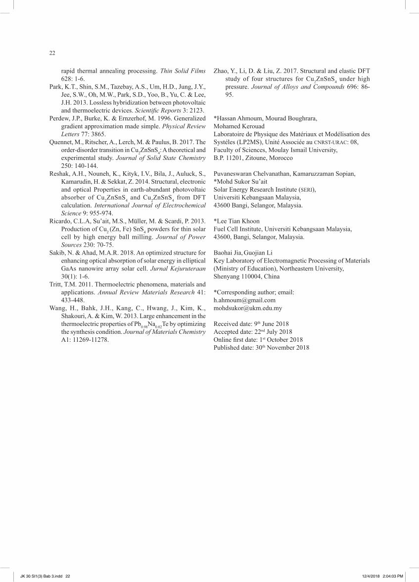
This contrary scenario between these parameters suggest the existence of a particular region where this material has a maximum efficiency of converting heat to electrical, for this reason we have calculated figure of merit see Figure 10, which is calculated by using the Equation (7);
α ω ω ω ω
α
( ) ( ) ( ) ( )
( ) /
= + −
= −
= = − −
2 2 2
1 2
0
e e e w
hv A hv E
P JV J J e
r i i
g
SC
eVKT 11
1 2
0
0 0
V
a E e
J e a E I dE
Je
fra E I dE
ZT
E L
SC sun
bb
( )
( )
( )
( )= −
=
=
=
−
∞
∞
∫
∫
α
π
σσ
η
S T
K
T T ZT
ZTTT
h c
c
h
2
1 1
1=
− + −
+ +
(7)
where σ, is conductivity electrical, S is Seebeck coefficient, T Temperature, k is thermal conductivity. At the room temperature we have found a value of 0.724, which is close to the value found in Cu2CdSnS4 (0.70) and Cu2CdSnTe4 (0.744) (Hussain et al. 2017). As we expect the figure of merit increase to a certain value of temperature which is 846 K, after the value start dramatically decrease. This could well mean that, this material has better efficiency at thermal
energy under 820 K. Finally, we have calculated the efficiency of converting heat to electricity by using the Equation (8) (Tritt 2011):
α ω ω ω ω
α
( ) ( ) ( ) ( )
( ) /
= + −
= −
= = − −
2 2 2
1 2
0
e e e w
hv A hv E
P JV J J e
r i i
g
SC
eVKT 11
1 2
0
0 0
V
a E e
J e a E I dE
Je
fra E I dE
ZT
E L
SC sun
bb
( )
( )
( )
( )= −
=
=
=
−
∞
∞
∫
∫
α
π
σσ
η
S T
K
T T ZT
ZTTT
h c
c
h
2
1 1
1=
− + −
+ + (8)
where Tc and Th are the temperatures on the hot and cold sides. By given this equation hot and cold side temperatures of 800 K and 100 K respectively, we found the efficiency conversion thermal is 12.136%.
FIGURE 9. Thermoelectric properties of simulated CZTS
FIGURE 10. Figure of merit of CZTS
JK 30 SI1(3) Bab 3.indd 20 12/4/2018 2:04:02 PM
21
CONCLUSION
In summary, we have successful studied the stannite phase of CZTS. We focus on the crystal structural, electronic structure, optical and thermoelectric properties. This study has been done using DFT+GGA functional implemented in quantum-espresso package. All obtained results are in excellent accord with experimental measurement, such the optical band gap (1.46 eV) and the coefficient absorption (105 cm–1) in the visible range, which make this material an excellent candidate to the photovoltaic application. Also, we have calculated the charge carrier concentration of holes (8.89 x 1019 cm–3), this value for CZTS semiconductor considered close to ideal value proposed by Mott criterion (David & Mott, 1970). Also, we have found figure of merit achieve to a maximum of 0.724 which also considered as good value of p-type semiconductor. From this investigation, we suggest that this material can be used as a multi-functional material in different application such as photovoltaic application and thermoelectric.
AcKnoWledgeMenT
This work has been supported by the URAC: 08 project PPR: (MESRSFC-CNRST) and also partially supported by Universiti Kebangsaan Malaysia (UKM) Young Researcher Incentive Grant (UKM-GGPM-2016-053). H. Ahmoum would also like to thank UKM for the attachment opportunity in UKM.
REFERENCES
Anisimov, V.I., Aryasetiawan, F. & Lichtenstein, A.I. 1997. First-principles calculations of the electronic structure and spectra of strongly correlated systems: the LDA+U method. Journal of Physics: Condensed Matter 9: 767-808.
David, A. & Mott, N.F. 1970. Conduction in non-crystalline systems V. Conductivity, optical absorption and photoconductivity in amorphous semiconductors. Philosophical Magazine 22(179): 903-922.
Fernandes, P.A., Salomé, P.M.P. & Cunha, A.F. 2011. Study of polycrystalline Cu2ZnSnS4 films by Raman scattering. Journal of Alloys and Compounds 509(28): 7600-7606.
Giannozzi, P., Baroni, S., Bonini, N., Calandra, M., Car, R., Cavazzoni, C., Ceresoli, D., Chiarotti, G.L., Cococcioni, M., Dabo, I., Dal Corso, A., de Gironcoli, S., Fabris, S., Fratesi, G., Gebauer, R., Gerstmann, U., Gougoussis, C., Kokalj, A., Lazzeri, M., Martin-Samos, L., Marzari, N., Mauri, F., Mazzarello, R., Paolini, S., Pasquarello, A., Paulatto, L., Sbraccia, C., Scandolo, S., Sclauzero, G., Seitsonen, A.P., Smogunov, A., Umari, P. & Wentzcovitch, R.M. 2009. Quantum espresso: A modular and open-source software project for quantum simulations of materials. Journal of Physics: Condensed Matter 21: 395502.
Gusain, M., Rawat, P. & Nagarajan, R. 2014. Solvent mediated rapid synthesis of orthorhombic Cu2ZnSnS4 (CZTS). Materials Letters 133: 220-223.
Hammi, M., El Rhazouani, O., Arejdal, M. & Slassi, A. 2017. Ab initio study of semi-classic transport coefficient of SnO2 thermoelectric material. Chinese Journal of Physics 55(1): 187-194.
Haq, B.U., Ahmed, R., Rhee, J., Shaari, A., Alfaifi, S. & Ahmed, M. 2017. composition-induced influence on the electronic band structure, optical and thermoelectric coefficients of the highly mismatched ganSb alloy over the entire range: A DFT analysis. Journal of Alloys and Compounds 693: 1020-1027.
Hou, X., li, Y., Yan, J.J. & Wang, c.W. 2014. Highly efficient photocatalysis of p-type Cu2ZnSnS4 under visible-light illumination. Materials Research Bulletin 60: 328-633.
Hussain, S., Murtaza, G., Khan, S.H., Khan, A., Ali, M.A., Faizan, M., Mahmood, A. & Khenata, R. 2016. First principle study of structural, optoelectronic and thermoelectric properties of Cu2CdSnX4 (X = S, Se, Te) chalcogenides. Materials Research Bulletin 79: 73-83.
Jackson, P., Hariskos, d., Wuerz, R., Wischmann, W. & Powalla, M. 2014. Compositional investigation of potassium doped Cu(In, Ga)Se2 solar cells with efficiencies up to 20.8%. Physica Status Solidi – Rapid Research Letters 8(3): 219-222.
Kumar, S., Ansari, M.Z. & Khare, n. 2018. Influence of compactness and formation of metallic secondary phase on the thermoelectric properties of Cu2ZnSnS4 thin films. Thin Solid Films 645: 300-304.
liu, M.l., Huang, F.Q., chen, l.d. & chen, I.W. 2009. A wide band gap p-type thermoelectric material based on quaternary chalcogenides of Cu2ZnSnQ4 (Q = S, Se). Applied Physics Letters 94(20): 202103.
Madsen, K.H.G. & Singh, D.J. 2016. BoltzTrap. A Code for calculating band-structure dependent quantities. Computer Physics Communications 175(1): 67-71.
Mahajan, S., Stathatos, E., Huse, N., Birajdar, R., Kalarakis, A. & Sharma, R. 2018. Low cost nanostructure kesterite cZTS thin films for solar cells application. Materials Letters 210: 92-96.
Mohamed, R., Yusop, A.M., Mohamed, A. & Nordin, N.I. 2016. Behavioral analysis of thermoelectric module under different configurations and temperature gradient. Jurnal Kejuruteraan 28: 19-27.
Monkhorst, H.J. & Pack, J.D. 1976. Special points for Brillouin-zone integrations. Physical Review B 13: 5188.
Mounkachi, O., Salmani, E., Mahhouti, Z., Hamedoun, M., Ez-Zahraouy, H., Benaissa, M. & Benyoussef, A. 2014. Accurate band gaps for earth-abundant photovoltaic absorber from density functional theory. In. International Renewable and Sustainable Energy Conference (IRSEC), IEEE. 1498548.
Olgar, M.A., Klaer, J., Mainz, R., Ozyuzer, L. & Unold, T. 2017. Cu2ZnSnS4-based thin films and solar cells by
JK 30 SI1(3) Bab 3.indd 21 12/4/2018 2:04:02 PM
22
rapid thermal annealing processing. Thin Solid Films 628: 1-6.
Park, K.T., Shin, S.M., Tazebay, A.S., Um, H.D., Jung, J.Y., Jee, S.W., oh, M.W., Park, S.d., Yoo, B., Yu, c. & lee, J.H. 2013. Lossless hybridization between photovoltaic and thermoelectric devices. Scientific Reports 3: 2123.
Perdew, J.P., Burke, K. & Ernzerhof, M. 1996. Generalized gradient approximation made simple. Physical Review Letters 77: 3865.
Quennet, M., Ritscher, A., Lerch, M. & Paulus, B. 2017. The order-disorder transition in Cu2ZnSnS4: A theoretical and experimental study. Journal of Solid State Chemistry 250: 140-144.
Reshak, A.H., Nouneh, K., Kityk, I.V., Bila, J., Auluck, S., Kamarudin, H. & Sekkat, Z. 2014. Structural, electronic and optical Properties in earth-abundant photovoltaic absorber of Cu2ZnSnS4 and Cu2ZnSnS4 from DFT calculation. International Journal of Electrochemical Science 9: 955-974.
Ricardo, C.L.A, Su’ait, M.S., Müller, M. & Scardi, P. 2013. Production of Cu2 (Zn, Fe) SnS4 powders for thin solar cell by high energy ball milling. Journal of Power Sources 230: 70-75.
Sakib, N. & Ahad, M.A.R. 2018. An optimized structure for enhancing optical absorption of solar energy in elliptical GaAs nanowire array solar cell. Jurnal Kejuruteraan 30(1): 1-6.
Tritt, T.M. 2011. Thermoelectric phenomena, materials and applications. Annual Review Materials Research 41: 433-448.
Wang, H., Bahk, J.H., Kang, c., Hwang, J., Kim, K., Shakouri, A. & Kim, W. 2013. large enhancement in the thermoelectric properties of Pb0.98Na0.02Te by optimizing the synthesis condition. Journal of Materials Chemistry A1: 11269-11278.
Zhao, Y., Li, D. & Liu, Z. 2017. Structural and elastic DFT study of four structures for Cu2ZnSnS4 under high pressure. Journal of Alloys and Compounds 696: 86-95.
*Hassan Ahmoum, Mourad Boughrara, Mohamed KerouadLaboratoire de Physique des Matériaux et Modélisation des Systéles (LP2MS), Unité Associée au CNRST-URAC: 08,Faculty of Sciences, Moulay Ismail University, B.P. 11201, Zitoune, Morocco
Puvaneswaran Chelvanathan, Kamaruzzaman Sopian, *Mohd Sukor Su’aitSolar Energy Research Institute (SERI), Universiti Kebangsaan Malaysia, 43600 Bangi, Selangor, Malaysia.
*Lee Tian Khoon Fuel Cell Institute, Universiti Kebangsaan Malaysia, 43600, Bangi, Selangor, Malaysia.
Baohai Jia, Guojian Li Key Laboratory of Electromagnetic Processing of Materials (Ministry of Education), Northeastern University, Shenyang 110004, China
*Corresponding author; email:[email protected]@ukm.edu.my
Received date: 9th June 2018Accepted date: 22nd July 2018online first date: 1st October 2018Published date: 30th November 2018
JK 30 SI1(3) Bab 3.indd 22 12/4/2018 2:04:03 PM