

Preface 5
Highlights of 2010 9
About CIC 13
Milestone 14
Mission and Vision 15
Organization and Manpower 16
Research and Development 19
MorPACK-Heterogeneous system Integration and Prototype Testing Platform 20 Introduction of MorPACK Platform 21
MorPACK system Design Process 24
Practical Results 29
R&D on Heterogeneous Chip Implementation Platform 31 Intelligent Sensing SoC Design Platform 31
(a) Use of CMOS MEMS material parameters to fi x the behavior simulation results of MEMS structure 32
(b) Co-simulation environment of MEMS structure and CMOS circuit 32
Intelligent sensing SoC Process Platform 33
(a) Front side CMOS MEMS process 33
(b) Inter-oxide etch CMOS MEMS process 34
(c) CMOS BioMEMS Process 34
Intelligent Sensing SoC Cutting/Package Platform 34
(a) Use Photo-resist to protect MEMS Structure 35
(b) On-wafer measurement 35
CMOS G-sensor IP Design Example 35
CMOS Resonator and Oscillator IP Design Example 37
CMOS Bio-medical Sensor Design Example 39
Conclusions 40
Patents 42
Papers 44 2010 Theses in International Journal (Journal Papers) 44
2010 Theses in International Conference (Conference Papers) 45
2010 Theses in Domestic Conference 47
Services 49
Design Environment Services 50 Chip and system Design Implementation Environment 50
Embedded system Design Implementation Environment 51
MorFPGA: Modularization FPGA Teaching & Contest common Platform 54
IC design and Manufacturing Service 56
Contents
2

3
CIC ANNUAL REPORT 2010
Chip Implementation Services 58 Processes for Prototyping IC Fabrication 58
Statistics of Services 61
Design Implementation Measurement Counseling Service (Hotline Service) 61
Measurement 63
Digital and Mixed-signal IC and System Testing Error-detection Environment 64
Analog, MEMS and Communication Chip Measurement Platform 68 Analog IC and MEMS IC Testing Platform 68
Achievements in 2010 68
For Analog chip measurement, the services currently provided by CIC include regular equipment and
high-level analog measurement 68
For MEMS measurement technology 70
CIC completed technology and measurement environment of bio-coating for bio-sensors
Communication Chip Measurement Platform 70
Training 77
Education Programs 78
E-Learning Courses 79
Contest 80 2010 IC Design Contest 80
2010 Code-O-Rama Design Contest 80
2010 University IC Computer-Aid Design (CAD) Contest 81
Publications 82
Public Education 83
The 2010 VLSI/CAD Special Session Organized by CIC 83
Activities and Events 85
21 VLSI Design/CAD Symposium and 2010 CIC Achievement Presentation 86
Contest and Award 88 4th NARL Excellent Contribution Award 88
Invention Award in“2010 Taipei International Invention Show & Technomart” 89
TSMC Manager Ge-Li Chen Award Ceremony 90
Promulgation Ceremony for Director General Tzi-Dar Chiueh 91
Meet the users 93
Imprint 96
CICCICICCICICICCICICICCICICICICICICICICICCCICICICICICICCICCCCCICICCICCICCICCICICC CCCCCCCCCCCCC CCCC CCCCCC CCCCC CCCCCCCCCC CC CCCCCC CC AAAANANANANNAAAAANANA NNNUNNUNUNUUNUNUUUNUUNUUUNUUUUUUUUUUUUUUAALALALALAAAAALAAAA RR R R EPPPPPPPEPPEPPPPPPPPPPPPPPPPE OROROROROOOOOO TTTT TT TT TTTT T 202000000000200200000020020202020202020020000020000200101101010101010101010101010001011010101010100
3
70

4

5
CIC ANNUAL REPORT 2010
6
In the era of the knowledge-based economy, high-quality human resources are the keys to enhancing the
competitiveness of a country. To make Taiwan a leading player in the global semiconductor market, for the past
two decades National Chip Implementation Center (CIC) has endeavored to provide academia in Taiwan services
in the following three major areas: IC/System design environments; chip fabrication, heterogeneous packaging
and measurement services; promotion of technology for IC/ System design and international collaboration.
In 2010, CIC integrated seven well-known IC/System design flows and 11 advanced processes for it
academic users. The advanced processes include four CMOS processes, two BiCMOS process, one GaAs
process, two CMOS MEMS processes, one CMOS BioMEMS process, and one high-voltage process. During
this period, the center helped to conduct 2783 IC design projects and to produce 1794 chips, including 187
educational chips and 1607 advanced chipsthrough local foundries. In addition, the center also helped to complete
testing/measurement of 1487 chips. More than 300 professors have benefi ted from the design and fabrication
environments provided by the center to produce 729 publications in international journals and conferences. In
2010, the center offered 164 training classes to 8423 students in 6 categories including Full-Custom IC design,
Cell-Based IC design, FPGA design, IC testing, RF/MMIC design, and CMOS MEMS design.
CIC will continue to collaborate with the academia, industries, and research institutes to cultivate more
high-quality researchers and designers, and to enhance the IC/System technology level so as to strengthen the
core competence of Taiwan’s SoC research.
6
Perface
7
CIC ANNUAL REPORT 2010
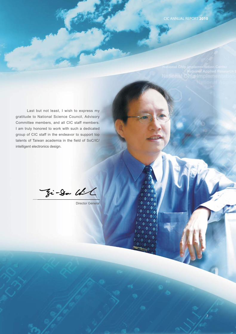
Last but not least, I wish to express my
gratitude to National Science Council, Advisory
Committee members, and all CIC staff members.
I am truly honored to work with such a dedicated
group of CIC staff in the endeavor to support top
talents of Taiwan academia in the field of SoC/IC/
intelligent electronics design.
7
CIC ANNUAL REPORT 2010
Director General

8

9
CIC ANNUAL REPORT 2010

10
Highlights of 2010
2010/10/19~11/01
2010/09/30~10/03
2010/11/01
2010/08/03~08/06
2010/07/05~09/08
2010/06/08~06/21
2010/05/28
2010/04/28~04/30
2010/01/08~03/12
2010/12/07~12/20
2010/12/13~12/15
11
CIC ANNUAL REPORT 2010
E-Learning Courses II
2010 Taipei International Invention Show & Technomart
Promulgation Ceremony for Director General Tzi-Dar Chiueh
2010 CIC Multi-Project Chip Workshop & 21th VLSI Design/CAD Symposium
CIC Summer Training Courses
E-Learning Courses Ⅰ
2010 CAD Contest
2010 IC Design Contest
CIC Spring Training Courses
E-Learning Courses III
CIC Business Presentation
12
13
CIC ANNUAL REPORT 2010
During recent decades, the focus of the
Taiwanese economy has shifted from traditional
industry to science and the high-tech industry. Despite
periodic recessions, Taiwan has invested hundreds
of billions of dollars in developing hi-tech products
such as computers, multimedia, networks, and so on.
Above all, the boom in information and semiconductor
manufacturing over the past decade has seen Taiwan
become one of the major players in the worldwide
electronics industry.
Nevertheless, Integrated Circuit (IC) has
remained the leading import in Taiwan since 1991.
IC has been labeled the rice of the electronics
industry, and is the key component for digitalizing and
minimizing electronic products, including information
and communication products, consumer electronics,
and so on. The high dependence of Taiwan on imported
ICs can be ascribed primarily to a shortage of domestic
manpower and a lag in developing critical IC design
technology. Consequently, Taiwan cannot even supply
its own demand for high value-added IC products, let
alone export to supply others.
Accordingly, the National Science Council,
based on the resolution of the Fourth National Science
and Technology Conference, init iated the Chip
Implementation Center Project (CIC Project) in 1992.
This project aims to establish a national research and
service center for IC design, namely CIC. To make
Taiwan a global IC design center, CIC is devoted to
cultivating IC design manpower and upgrading IC
design technology in Taiwan.
141414
Milestones
■ May 1992 The National Science Council initiated the Chip Implementation Center Project (CIC Project).
■ January 1993 The Project offi ce, under the control of Dr. Jen-Sheng Hwang, was established on Technology Road of the Hsinchu Science Park.
■ October 1999 CIC was located on Prosperity Road of Hsinchu Science Park.
■ August 2000 Dr. Chen-Yi Lee was appointed Director General of CIC.
■ September 2002 The south region offi ce of CIC was inaugurated in the Tainan Science Park.
■ June 2003 CIC became one of the centers under the framework of the National Applied Research Laboratory (NARL).
■ February 2004 Dr. Jing-Yang Jou was appointed Director General of CIC.
■ November 2004 CIC was relocated to the Nano Electronics Research Building in the Hsinchu Science Park.
■ May 2006 CIC passed the periodical tracking of ISO 9001:2000 quality system.
■ June 2006 Dr. Chin-Long Wey was appointed Director General of CIC.
■ August 2007 CIC acquired ISO/IEC 27001:2005 certifi cation.
■ October 2007 The south region offi ce of CIC was relocated to the Chi Mei building in National Cheng Kung University.
■ November 2010 Dr. Tzi-Dar Chiueh was appointed Director General of CIC.
15
CIC ANNUAL REPORT 2010CIC ANNUAL REPORT 2010
15
Mission and Vision
In the era of the knowledge-based economy, manpower and technology are the keys to enhancing
industrial competitiveness. With a view to making Taiwan a leading player in the global semiconductor market, CIC
is continuing to focus on developing human resources and advanced technologies. To achieve these objectives,
CIC focuses its efforts on the following four main areas:
■ Providing an IC/ system design environment;
■ Providing chip fabrication and measurement services;
■ Promoting technology for IC/ system design and international collaborations;
■ Improving IC/ system design services in southern Taiwan.
◎ Accomplishments
■ CIC achieved signifi cant results in all four of its main missions during 2008.
■ In relation to providing IC/ system design services, the center integrated nine well-known IC/ system design
fl ows and serviced 2303 hotline callers from academia.
■ In relation to providing IC fabrication and measurement services, the center helped produce 1794 chips,
including 187 educational chips and 1607 advanced process chips.
■ In relation to promoting IC/ system design technology, the center offered 164 courses to 8423 students.
■ In relation to improving IC/ system design services in southern Taiwan, the center provided 615 measurement
services to academia and industry in southern Taiwan.
◎ Vision
CIC aims to become a world-class laboratory for IC/ system design research and service in Taiwan.
1616
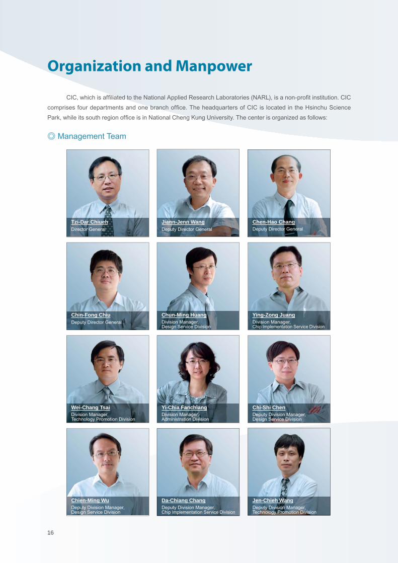
CIC, which is affi liated to the National Applied Research Laboratories (NARL), is a non-profi t institution. CIC
comprises four departments and one branch offi ce. The headquarters of CIC is located in the Hsinchu Science
Park, while its south region offi ce is in National Cheng Kung University. The center is organized as follows:
◎ Management Team
Organization and Manpower
Tzi-Dar ChiuehDirector General
Chun-Ming HuangDivision Manager, Design Service Division
Yi-Chia FanchiangDivision Manager, Administration Division
Da-Chiang ChangDeputy Division Manager,Chip Implementation Service Division
Jiann-Jenn WangDeputy Director General
Ying-Zong JuangDivision Manager, Chip Implementation Service Division
Chi-Shi ChenDeputy Division Manager, Design Service Division
Chen-Hao ChangDeputy Director General
Chin-Fong ChiuDeputy Director General
Wei-Chang TsaiDivision Manager, Technology Promotion Division
Chien-Ming WuDeputy Division Manager,Design Service Division
Jen-Chieh WangDeputy Division Manager,Technology Promotion Division

17
CIC ANNUAL REPORT 2010
17
66.37
15.93
17.70
26.55
61.95
8.85
2.65
Types of Personnel Total Percentage
Researchers 75 66.37 %
Technical Personnel 18 15.93 %
Other Personnel 20 17.70 %
Total 113 100 %
Table 2 - Statistics of Degree Holders at CIC
Table 1 - Statistics of Staff at CIC
Degree Total Percentage
Ph.D. 10 8.85 %
Master 70 61.95 %
Bachelor 30 26.55 %
College 3 2.65 %
Total 113 100 %
Figure 1 - Statistics of Staffs at CIC■ Researcher ■ Technical Personnel ■ Other Personnel
Figure 2 - Statistics of Degree Holders at CIC■ Ph.D. ■ Master ■ Bachelor ■ College
◎ Manpower
2010, CIC had 113 employees. Table 1 and Fig.1 show that 75 (66.4%) of these employees are fulltime
researchers, while 18 (15.9%) are technical support personnel.
Seventy (62%) of the center employees have acquired master’s degrees and ten (8.9%) have PhDs, as
listed in Table 2, mostly in electronics, electrical engineering, and computer science. Figure 2 shows that over two
thirds of center staff held master’s or doctoral degrees in research and development

1818

19
CIC ANNUAL REPORT 2010
19
CIC ANNUAL REPORT 2010
2020
The IC industry is one of the most important industries in Taiwan, with a gross output value of NTD 1,347.3
billion. In recent years, along with the continuous progress in semiconductor process and design automation
technology, the concept of system-on-Chip (SoC), namely applying single chip to realize complex systems, is
no longer a dream. Given the enormous infl uence of SoC on future industries, the government of Taiwan has
invested heavily and planed the“National Si-Soft Project,”with a total budget of NTD 7.6 billion, to promote
a fresh development leap for Taiwanese industry. With the support of the“National Science & Technology
Program for System-on-Chip (NSoC),”Taiwanese academia has established SoC R&D centers in universities,
including NTU, NTHU, NCTU, NCKU, NCCU, NCHU, NCU, etc. Furthermore, significant manpower has been
invested in research on SoC-related issues. However, SoC R&D teams established by academics in Taiwan have
encountered extreme difficulties in the phase of practice and test for IC chips. In order to help domestic SoC
teams apply their research results in physical IC chips, CIC has proposed the concept of“Multi-Project SoC (MP-
SoC)”, and won the great honor of 2nd place (Taiwan Xue Mountain) in the Outstanding Research Award during
the inaugural NARL Excellent Contribution Awards in Science and Technology, held in 2007. However, although
the MP-SoC concept was effective, the tap-out expenses were still high for chips with MP-SoC design, and such
chips also had heavy design personnel requirements; nonetheless, MP-SoC design could not easily achieve the
goal of heterogeneous integration.
Along with the trends of global warming, an aging population and artificial intelligence, the『National
Intelligent Electronics Program (NIE Program)』regards MG+4C (Medical Electrical Equipment, Green Energy
Electrical Equipment, Car Electronics and 3C Electrical Products) as its priority development strategy, and expects
to promote the IC design industry and transform it into an advanced industry. However, academic circles are
currently emphasizing research on the Silicon Intellectual Property (IP) of specific applications, and complete
system support continues to be required for fi nalizing applications of 『MG+4C』, including core chip and core
PCB. Current prototype platforms include (a) FPGA-based prototype platform, which cannot integrate hard IP
and performs poorly; hybrid prototype platform is currently commonly used in industry. Core hard IP is a form of
infl exible real chip. FPGA continues to perform poorly, as does the virtual prototype platform, which cannot be
physically verifi ed. The fully customized prototype platform is extremely costly in terms of money and development
time. To solve this problem, CIC thus has proposed MorPACK, a heterogeneous system integration and prototype
testing platform.
The National Chip Implementation Center (CIC) of NARL undertook the mission of building the R&D
platform, supporting academic research, and promoting advanced technology to actively develop a R&D
integration platform based around applications of MG+4C. CIC employed the concept of common use and reuse,
and also controlled the key technologies, including die-level modularization, three-dimensional (3D) module
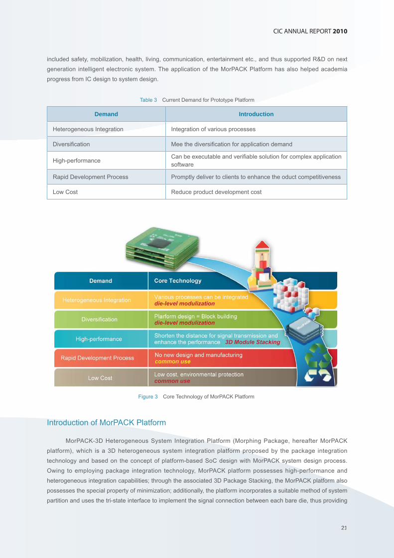
stacking etc., to develop the transformer of system R&D platform—MorPACK (Morphing + Package). Table 3
lists current demand of academia / industry for the prototype platform, and Fig.3 shows the core technologies
that the MorPACK Platform proposed to meet current demand for the prototype platform. The MorPACK Platform
has employed the core technologies, including die-level modularization, 3D module stacking and common use,
to equip it with the properties of heterogeneous integration, diversifi cation, high-performance, rapid development
process and low cost, which have infinite possibilities for use in various applications. The application scope
MorPACK-Heterogeneous system
Integration and Prototype Testing Platform
21
CIC ANNUAL REPORT 2010
21
included safety, mobilization, health, living, communication, entertainment etc., and thus supported R&D on next
generation intelligent electronic system. The application of the MorPACK Platform has also helped academia
progress from IC design to system design.
Table 3 Current Demand for Prototype Platform
Demand Introduction
Heterogeneous Integration Integration of various processes
Diversifi cation Mee the diversifi cation for application demand
High-performanceCan be executable and verifi able solution for complex application software
Rapid Development Process Promptly deliver to clients to enhance the oduct competitiveness
Low Cost Reduce product development cost
Figure 3 Core Technology of MorPACK Platform
Introduction of MorPACK Platform
MorPACK-3D Heterogeneous System Integration Platform (Morphing Package, hereafter MorPACK
platform), which is a 3D heterogeneous system integration platform proposed by the package integration
technology and based on the concept of platform-based SoC design with MorPACK system design process.
Owing to employing package integration technology, MorPACK platform possesses high-performance and
heterogeneous integration capabilities; through the associated 3D Package Stacking, the MorPACK platform also
possesses the special property of minimization; additionally, the platform incorporates a suitable method of system
partition and uses the tri-state interface to implement the signal connection between each bare die, thus providing
2222
the MorPACK system with better scalability for system accessories, as well as the ability to cheaply renew die
fl exibility in response to user demand. Teachers and students thus can focus on developing their own accelerator
die designs, and on using package integration technology to integrate their developed accelerator die design into
the MorPACK common platform so as to rapidly complete the SoC module. The proposed 3D Heterogeneous
System Integration Platform can not only solve and improve the defects of MP-SoC, but can also solve the
diffi culties faced by academic SoC teams in practically verifying SoC.
SDRAM NOR Flash
SDRAMController
NORController
Arbiter/Decoder
VGA(S) (M)
SRAM ROMTri-state
IO
AHB
NorthBridge
AcceleratorTri-state
IO
Accelerator
Tri-stateIO
ARM CPU
CPU
InterruptController
TimersPause/Remap
WDT U ART GPIO
APBBridge
Tri-stateIO SouthBridge
APB
Figure 4 Logic Framework of MorPACK system Platform
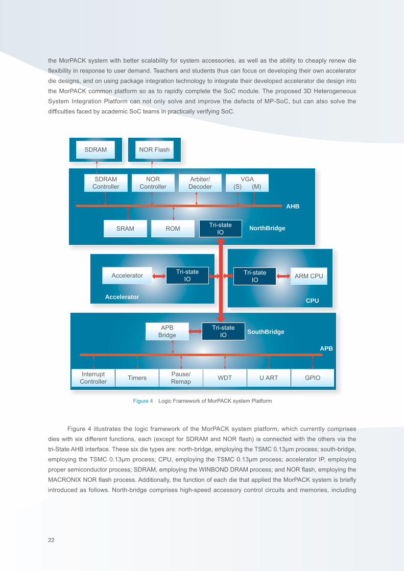
Figure 4 illustrates the logic framework of the MorPACK system platform, which currently comprises
dies with six different functions, each (except for SDRAM and NOR fl ash) is connected with the others via the
tri-State AHB interface. These six die types are: north-bridge, employing the TSMC 0.13μm process; south-bridge,
employing the TSMC 0.13μm process; CPU, employing the TSMC 0.13μm process; accelerator IP, employing
proper semiconductor process; SDRAM, employing the WINBOND DRAM process; and NOR fl ash, employing the
MACRONIX NOR fl ash process. Additionally, the function of each die that applied the MorPACK system is briefl y
introduced as follows. North-bridge comprises high-speed accessory control circuits and memories, including
23
CIC ANNUAL REPORT 2010
23
the arbiter and decoder circuits for AHB bus, SDRAM controller, NOR flash controller, VGA controller, SRAM,
and ROM. Owing to both arbiter and decoder of AHB bus being located in north-bridge, the number of master
and slave IPs can be scalable for the MorPACK system and is determined using the north-bridge chip; south-
bridge comprises some basic slow-speed accessory control circuits, including APB bridge, interrupt controller,
timers, pause/remap, watch dog timer, UART and GPIO; CPU realizes ARM926EJ_1616 processor core, which
possesses 16Kbytes instruction cache and 16Kbytes data cache, and connects with 2 units of 64Kbytes SRAM
as the instruction TCM and data TCM through two sets of tightly-coupled memory interface (hereinafter referred to
as the TCM interface). Furthermore, ARM926EJ_1616 possessed two units of the AHB bus interface: instruction
AHB and data AHB, which were combined into a single outward tri-state AHB interface to reduce the number of
pin-outs for CPU. The accelerator IP die is used as the hardware accelerator for the platform. Furthermore, the
SDRAM die is used as the memory buffer during platform operation and computation. Finally, the NOR fl ash die is
used to store and save the boot program and related application program.
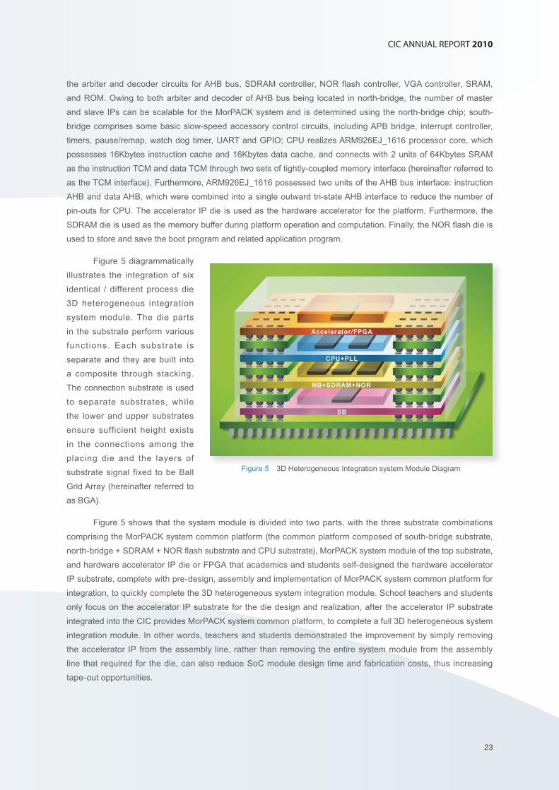
Figure 5 diagrammatically
illustrates the integration of six
identical / different process die
3D heterogeneous integration
system module. The die parts
in the substrate perform various
funct ions. Each substrate is
separate and they are built into
a composite through stacking.
The connection substrate is used
to separate substrates, while
the lower and upper substrates
ensure sufficient height exists
in the connections among the
placing die and the layers of
substrate signal fixed to be Ball
Grid Array (hereinafter referred to
as BGA).
Figure 5 shows that the system module is divided into two parts, with the three substrate combinations
comprising the MorPACK system common platform (the common platform composed of south-bridge substrate,
north-bridge + SDRAM + NOR fl ash substrate and CPU substrate), MorPACK system module of the top substrate,
and hardware accelerator IP die or FPGA that academics and students self-designed the hardware accelerator
IP substrate, complete with pre-design, assembly and implementation of MorPACK system common platform for
integration, to quickly complete the 3D heterogeneous system integration module. School teachers and students
only focus on the accelerator IP substrate for the die design and realization, after the accelerator IP substrate
integrated into the CIC provides MorPACK system common platform, to complete a full 3D heterogeneous system
integration module. In other words, teachers and students demonstrated the improvement by simply removing
the accelerator IP from the assembly line, rather than removing the entire system module from the assembly
line that required for the die, can also reduce SoC module design time and fabrication costs, thus increasing
tape-out opportunities.
Figure 5 3D Heterogeneous Integration system Module Diagram
2424
MorPACK system Design Process
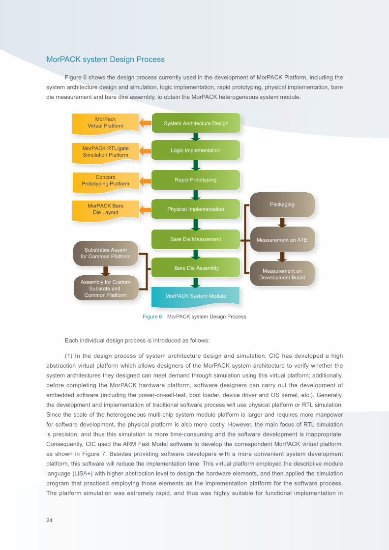
Figure 6 shows the design process currently used in the development of MorPACK Platform, including the
system architecture design and simulation, logic implementation, rapid prototyping, physical implementation, bare
die measurement and bare dire assembly, to obtain the MorPACK heterogeneous system module.
MorPackVirtual Platform
MorPACK RTL/gateSimulation Platform
ConcordPrototyping Platform
MorPACK BareDie Layout
System Architecture Design
Logic Implementation
Rapid Prototyping
Physical Implementation
Bare Die Measrement
Bare Die Assembly
MorPACK System Module
Substrates Assemfor Common Platform
Assembly for CustomSubsrate and
Common Platform
Packaging
Measurement on ATE
Measurement onDevelopment Board
Figure 6 MorPACK system Design Process
Each individual design process is introduced as follows:
(1) In the design process of system architecture design and simulation, CIC has developed a high
abstraction virtual platform which allows designers of the MorPACK system architecture to verify whether the
system architectures they designed can meet demand through simulation using this virtual platform; additionally,
before completing the MorPACK hardware platform, software designers can carry out the development of
embedded software (including the power-on-self-test, boot loader, device driver and OS kernel, etc.). Generally,
the development and implementation of traditional software process will use physical platform or RTL simulation.
Since the scale of the heterogeneous multi-chip system module platform is larger and requires more manpower
for software development, the physical platform is also more costly. However, the main focus of RTL simulation
is precision, and thus this simulation is more time-consuming and the software development is inappropriate.
Consequently, CIC used the ARM Fast Model software to develop the correspondent MorPACK virtual platform,
as shown in Figure 7. Besides providing software developers with a more convenient system development
platform, this software will reduce the implementation time. This virtual platform employed the descriptive module
language (LISA+) with higher abstraction level to design the hardware elements, and then applied the simulation
program that practiced employing those elements as the implementation platform for the software process.
The platform simulation was extremely rapid, and thus was highly suitable for functional implementation in

25
CIC ANNUAL REPORT 2010
25
software processes. Taking the software process of system function test as an example, it takes approximately
10 minutes to complete the simulation for the abovementioned RTL implementation platform, but only 5 seconds
to implement the same software process using the virtual platform. Therefore, the MorPACK virtual platform
is extremely convenient and offers significant time savings for software developers. Figure 8 (a) shows the
simulation result of the MorPACK RTL platform, and Fig.8 (b) illustrates the simulation result for the MorPACK
virtual platform; comparison shows no significant difference between the functions of the virtual platform,
built using Fast Model, and the RTL designed system. However, the latter took just 5 seconds to perform the
simulation, compared to 10 minutes for the former, representing a huge difference.
Figure 7 MorPACK Virtual Platform
Figure 8 MorPACK Virtual Platform
(a) (b)

2626
(2) In the process of logic and implementation design, CIC determined the architecture based on the
system level and used hardware descriptive language to implement the logic design and implementation for
MorPACK. This design process includes logic synthesis and implementation, and can yield the MorPACK RTL/
gate-level design and simulation platform.
(3) For the design process of rapid prototyping implementation, CIC used the self-developed SoC rapid
prototyping implementation platform (Concord) to proceed the prototyping implementation for each die of
MorPACK before tap-out. The Concord platform is employed to assure consistency between the architecture
of the implementation system and the framework of the future MorPACK chip system platform; additionally, the
rapid prototyping implementation of Concord platform for the MorPACK design can solve problems such as the
insufficient『flexibility』, the rapid prototype testing platform in the current market, and the inability to assure
consistency between the implementing system architecture and the framework of the future MorPACK chip
system platform. CIC thus has used the Concord platform to conduct prototyping implementation for MorPACK
system design.
(4) As for the software development environment, to make software development more convenient for
the MorPACK Platform, the introduction of embedded operating system has become increasingly important.
Therefore, CIC has established a related development and testing environment for embedded system software,
and has also implanted the updated Linux 2.6.33 operating system core to support resource management for
the MorPACK system. Currently, CIC has successfully implanted the Linux 2.6.33 operating system core into the
MorPACK platform, increasing the convenience of the development and implementation of software application
and hardware testing programs using this platform. Besides the implantation of the operating system and the
establishment of the development environment, to coordinate the character of the hardware of each system
module, CIC has also developed respondent boot ROM and boot loader for each system module. After starting,
the boot ROM allows the system module to be correctly set for each module status, ensures the normal operation
of each module, or conducts related POST (power-on-self-test) for each module, including the related reading and
writing tests administered to controllers of GPIO, timer, interrupt, remap/pause, watchdog, UART, SRAM, as well
Figure 9 Starting Screen of Boot ROM and Boot Loader for MorPACK
27
CIC ANNUAL REPORT 2010
27
as outside memories of SDRAM and fl ash, and then
provides the testing report as feedback. The boot
loader program is for setting the related software
and hardware environment, and loading information
on the operating system core and related fi le system
to manage resources and maintain normal system
operations. Currently, all MorPACK Platforms have
their own respondent boot ROM and boot loader
programs to assist them with booting and loading
the operating system. Figure 9 shows the starting
screen of the MorPACK boot ROM and boot loader;
moreover, Fig.10 illustrates the Linux starting screen
of the MorPACK.
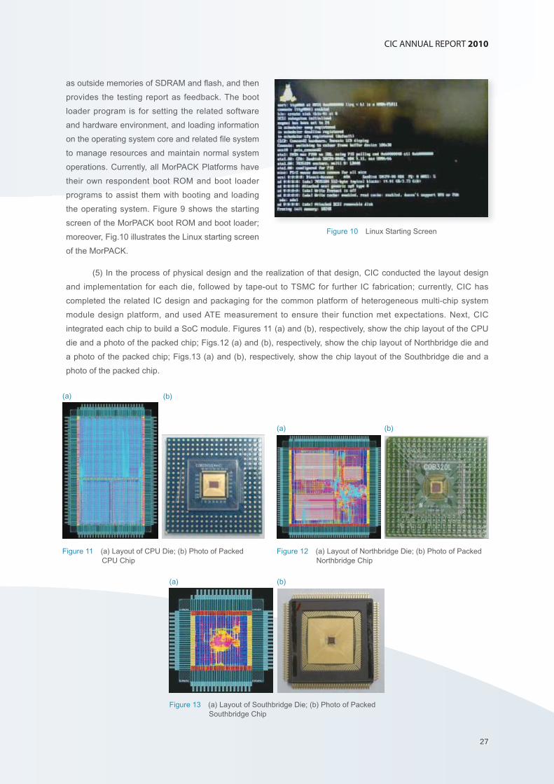
(5) In the process of physical design and the realization of that design, CIC conducted the layout design
and implementation for each die, followed by tape-out to TSMC for further IC fabrication; currently, CIC has
completed the related IC design and packaging for the common platform of heterogeneous multi-chip system
module design platform, and used ATE measurement to ensure their function met expectations. Next, CIC
integrated each chip to build a SoC module. Figures 11 (a) and (b), respectively, show the chip layout of the CPU
die and a photo of the packed chip; Figs.12 (a) and (b), respectively, show the chip layout of Northbridge die and
a photo of the packed chip; Figs.13 (a) and (b), respectively, show the chip layout of the Southbridge die and a
photo of the packed chip.
Figure 10 Linux Starting Screen
Figure 11 (a) Layout of CPU Die; (b) Photo of Packed CPU Chip
Figure 12 (a) Layout of Northbridge Die; (b) Photo of Packed Northbridge Chip
Figure 13 (a) Layout of Southbridge Die; (b) Photo of Packed Southbridge Chip
(a)
(a)
(b)
(b)
(a) (b)
2828
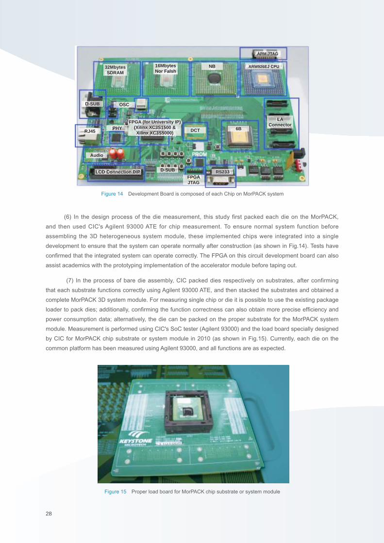
(6) In the design process of the die measurement, this study first packed each die on the MorPACK,
and then used CIC's Agilent 93000 ATE for chip measurement. To ensure normal system function before
assembling the 3D heterogeneous system module, these implemented chips were integrated into a single
development to ensure that the system can operate normally after construction (as shown in Fig.14). Tests have
confi rmed that the integrated system can operate correctly. The FPGA on this circuit development board can also
assist academics with the prototyping implementation of the accelerator module before taping out.
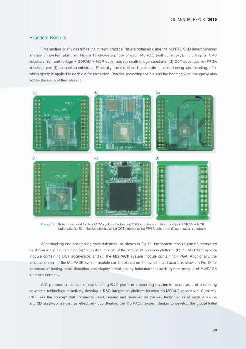
(7) In the process of bare die assembly, CIC packed dies respectively on substrates, after confirming
that each substrate functions correctly using Agilent 93000 ATE, and then stacked the substrates and obtained a
complete MorPACK 3D system module. For measuring single chip or die it is possible to use the existing package
loader to pack dies; additionally, confi rming the function correctness can also obtain more precise effi ciency and
power consumption data; alternatively, the die can be packed on the proper substrate for the MorPACK system
module. Measurement is performed using CIC's SoC tester (Agilent 93000) and the load board specially designed
by CIC for MorPACK chip substrate or system module in 2010 (as shown in Fig.15). Currently, each die on the
common platform has been measured using Agilent 93000, and all functions are as expected.
ARM JTAG
ARM926EJ CPU
LAConnector
NB16MbytesNor Falsh
32MbytesSDRAM
D-SUB
RJ45PHY
OSC
FPGA (for University IP)(Xilinx XC3S1500 &Xilinx XC3S5000)
Audio
LCD Connection DIP
DCT 6B
FPGAJTAG
RS233D-SUB
Figure 14 Development Board is composed of each Chip on MorPACK system
Figure 15 Proper load board for MorPACK chip substrate or system module
29
CIC ANNUAL REPORT 2010
29
Practical Results
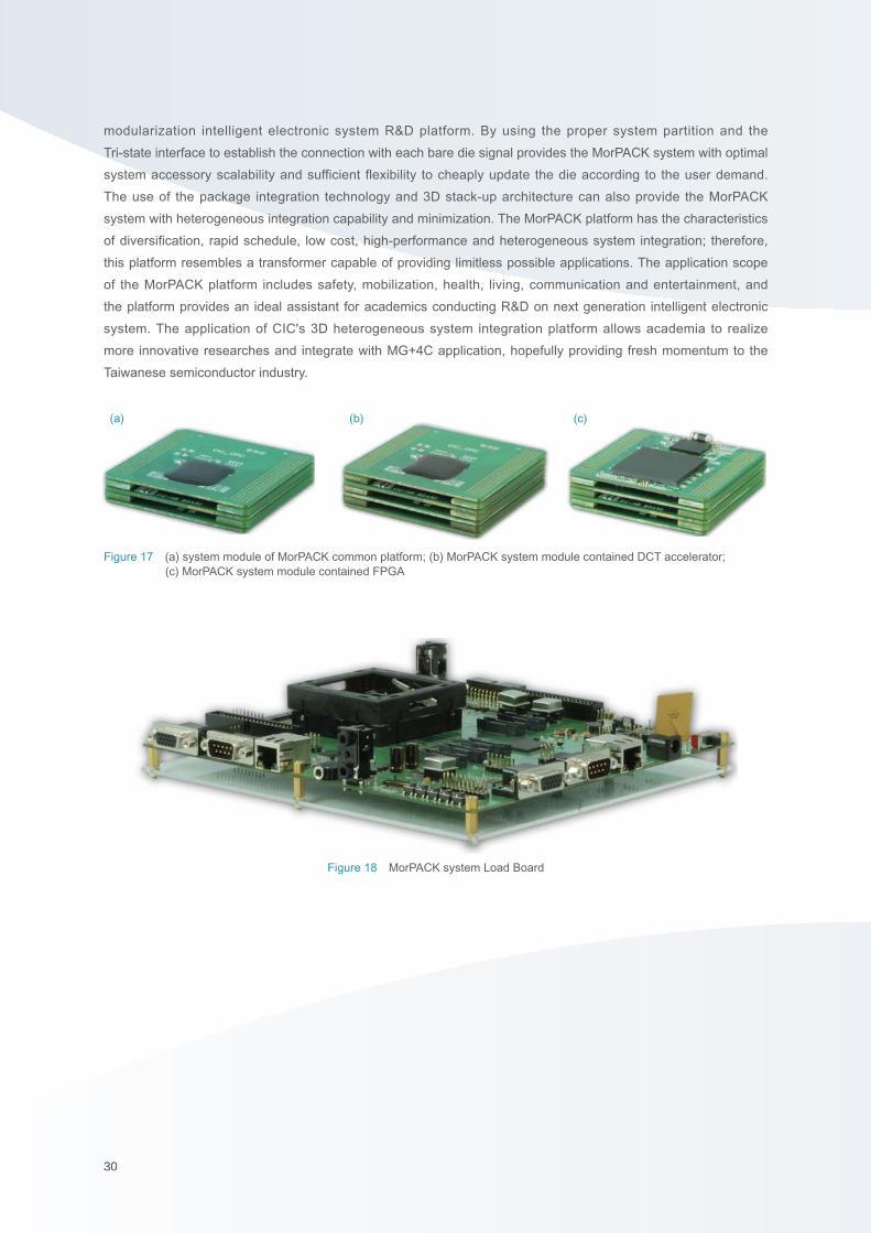
This section briefl y describes the current practical results obtained using the MorPACK 3D heterogeneous
integration system platform. Figure 16 shows a photo of each MorPAC (without epoxy), including (a) CPU
substrate, (b) north-bridge + SDRAM + NOR substrate, (c) south-bridge substrate, (d) DCT substrate, (e) FPGA
substrate and (f) connection substrate. Presently, the die of each substrate is packed using wire bonding, after
which epoxy is applied to each die for protection. Besides protecting the die and the bonding wire, the epoxy also
solves the issue of their storage.
(a) (b) (c)
(d) (e) (f)
Figure 16 Substrates used for MorPACK system module. (a) CPU substrate; (b) Northbridge + SDRAM + NOR substrate; (c) Southbridge substrate; (d) DCT substrate; (e) FPGA substrate; (f) connection substrate
After stacking and assembling each substrate, as shown in Fig.16, the system module can be completed
as shown in Fig.17, including (a) the system module of the MorPACK common platform, (b) the MorPACK system
module containing DCT accelerator, and (c) the MorPACK system module containing FPGA. Additionally, the
practical design of the MorPACK system module can be placed on the system load board as shown in Fig.18 for
purposes of testing, error-detection and display. Initial testing indicates that each system module of MorPACK
functions correctly.
CIC pursued a mission of establishing R&D platform supporting academic research, and promoting
advanced technology to actively develop a R&D integration platform focused on MG+4C application. Currently,
CIC uses the concept that commonly used, reused and reserved as the key technologies of modularization
and 3D stack-up, as well as effectively coordinating the MorPACK system design to develop the global initial
3030
modularization intelligent electronic system R&D platform. By using the proper system partition and the
Tri-state interface to establish the connection with each bare die signal provides the MorPACK system with optimal
system accessory scalability and sufficient flexibility to cheaply update the die according to the user demand.
The use of the package integration technology and 3D stack-up architecture can also provide the MorPACK
system with heterogeneous integration capability and minimization. The MorPACK platform has the characteristics
of diversifi cation, rapid schedule, low cost, high-performance and heterogeneous system integration; therefore,
this platform resembles a transformer capable of providing limitless possible applications. The application scope
of the MorPACK platform includes safety, mobilization, health, living, communication and entertainment, and
the platform provides an ideal assistant for academics conducting R&D on next generation intelligent electronic
system. The application of CIC's 3D heterogeneous system integration platform allows academia to realize
more innovative researches and integrate with MG+4C application, hopefully providing fresh momentum to the
Taiwanese semiconductor industry.
(a) (b) (c)
Figure 17 (a) system module of MorPACK common platform; (b) MorPACK system module contained DCT accelerator; (c) MorPACK system module contained FPGA
Figure 18 MorPACK system Load Board
31
CIC ANNUAL REPORT 2010
31
R&D on Heterogeneous Chip
Implementation Platform
CIC of NARL is committed to intelligent sensing SoC technology, a simple CMOS Micro Electro-Mechanical
systems (MEMS) process, the development of related design, and implementation fl ow to fabricate diverse sensor
integration chip. Currently CIC had gained great achievement in development of process, chip cutting, packaging,
and reliability, in which the layout of relevant patents are proceeded with. CIC has obtained four patents in Taiwan
and US, and another 13 patents are still pending. Furthermore, CIC has published 27 papers in well-known
journals and conferences. By establishing the co-simulation environment of MEMS structure and CMOS circuit,
CIC has completed the transfer of the IP and technology for two CMOS accelerometers to the NCTU / Si-Soft
Research Center, and then provided the industrial implementation by Si-Soft Research Center. CIC possesses the
mass-production technology capabilities for developing MEMS commercialized products.
CIC developed the following specifi c technologies to complete intelligent sensing SoC design.
1. Intelligent Sensing SoC Design Platform
Regarding the development of the intelligent sensing SoC, it should essentially comprise two parts:
the micro-sensing structure itself, and the read-out circuit. Since comparison of sensor read-out circuit with
other items such as digital / analog converter reveals differences, for example in demand for cross-domain
talents, it is important to understand how to identify the MEMS process, in addition, people who can understand
the mechanical design as well as the analog and digital circuit design were relatively not many, and thus
it is difficult to independently design the reading circuit of sensors for them and makes them to encounter
with bottleneck. Additionally, experience of design and simulation for heterogeneous integration does not lie
within the expertise of a traditional IC design company. Furthermore, it's often necessary for optimal sensor
design to correct sensor characteristics by rear-end circuit which only experienced IC design companies
can resolve. The best solution thus is to create a sensor module (sensor IP) that contains both micro-
sensing structure and reading circuit. The output signal then can be processed via the analog or even the
digital signal.
Design of a sensing system starts from specifying it that requires evaluation of market size, merits
of competitors, design cost, and design period, etc. Chip design is performed after deciding specifications
of sensor IP or sensor integration chip. In the initial phase of CMOS MEMS sensor design, designers
cooperate to discuss the sensor models used (capacitive, voltage-type, etc.), signal magnitude and detection
of signal magnitude change, etc. In the next step, individual designs of sensor structure and circuit are
performed. After completing the design, MEMS structure and CMOS circuit are needed to be co-simulated
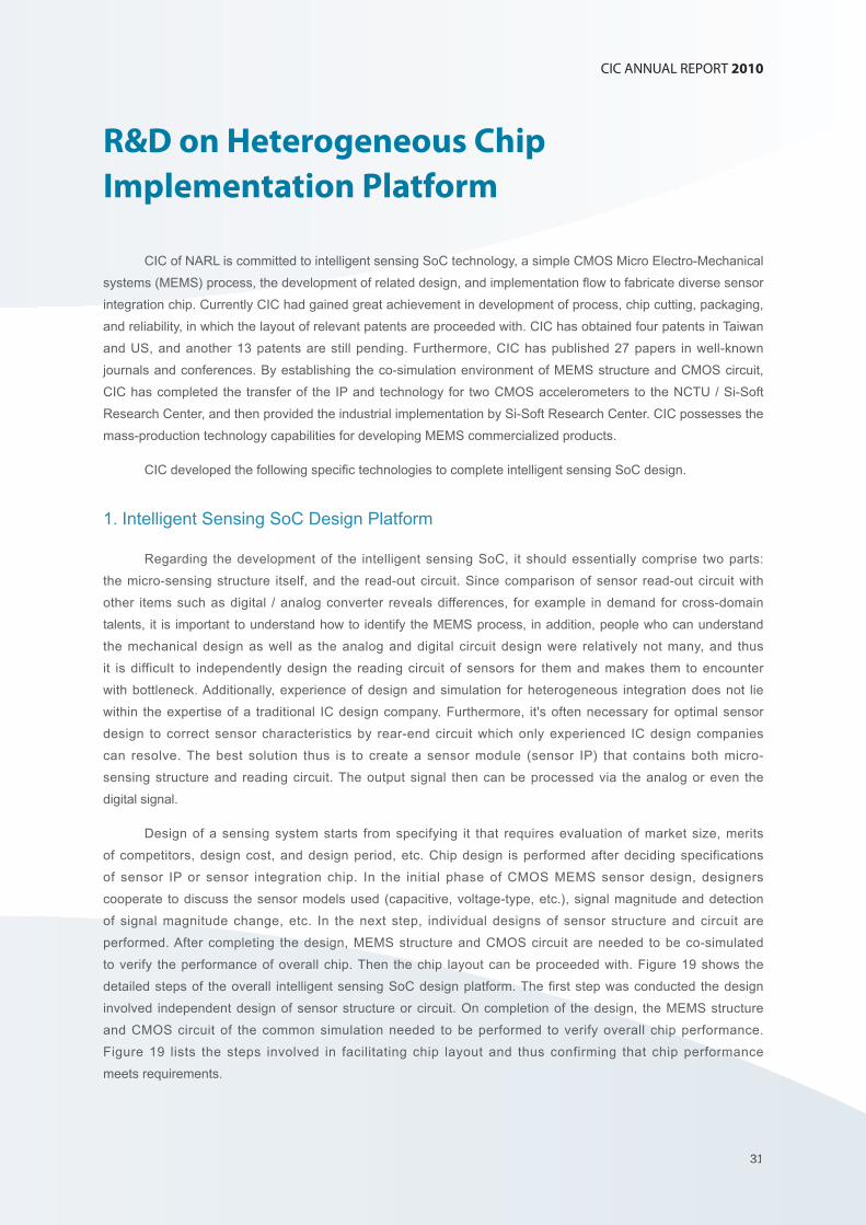
to verify the performance of overall chip. Then the chip layout can be proceeded with. Figure 19 shows the
detailed steps of the overall intelligent sensing SoC design platform. The first step was conducted the design
involved independent design of sensor structure or circuit. On completion of the design, the MEMS structure
and CMOS circuit of the common simulation needed to be performed to verify overall chip performance.
Figure 19 lists the steps involved in facilitating chip layout and thus confirming that chip performance
meets requirements.

3232
The general MEMS design process requires commercial software that supports the structure design, to
create 3D models, simulate MEMS structure behavior and simulate MEMS structure with a simple circuit. In the
fi eld of intelligent sensing SoC design platform, CIC possessed 2 unique features which they have sorted out the
material parameters used by the two largest CMOS wafer foundries in the world, and these parameters correct the
MEMS structure behavior simulation results. Additionally, complete circuit can be simulated with the co-simulation
environment of MEMS structure and CMOS circuit established by CIC.
(a) Use of CMOS MEMS material parameters to fi x the behavior simulation results of MEMS structure
Since the CMOS MEMS were based on establishing the CMOS process platform; thus, on the structure
design of CMOS MEMS, there are many materials properties and the structure consideration that will be affected
by the quality and the characteristics of CMOS process. However, when front-end CMOS process manufacturers
are developing the CMOS platform, they usually focused solely on the requirements for the electronic component
characteristics as its electrical quality (such as gate leakage current, dielectric material factor, etc.) Therefore
they cannot acquire the structure characteristics of related materials (such as residual stress, stress gradient and
Young's Modulus) from the database of original CMOS foundries. At present, CIC had verifi ed the 0.35μm and
0.18μm CMOS MEMS platform with extracting process parameters from 8 runs of chip implementation, as well as
integrated those related results into the process platform environment of CIC, as the reference to make correction
for designs. Additionally, CIC began using a modifi ed database of material parameters, and more complex and
unifi ed MEMS components for comparison and correction of parameters, with a view to conducting more accurate
simulation and analysis of relevant characteristics of MEMS components and systems. These results were
presented at the international Conference 2010 APCOT.
CIC has accumulated considerable experiences regarding the material parameter extraction and analysis;
therefore, including TSMC and UMC, many manufacturers have talked and negotiated with CIC for further
cooperation which will have important contribution to assist these manufacturers to enter MEMS foundry business
in the future.
(b) Co-simulation environment of MEMS structure and CMOS circuit
For the design of sensor and the read-out circuit, because of their different physical values; therefore,
effective and correct implementation of the co-simulation has always been a challenge for EDA software company.
CIC replaced real design fi les with behavior-descriptive models, while the language used to describe the sensor
behavior must also be considered the compatibility with the rear-end circuit simulation software. In the following
example, CIC uses a top-down approach to create efficient designs that realize stage simulation, and uses
Verilog-AMS to simulate the entire action of sensor IP. Verilog-AMS is one of behavioral descriptive languages
which can be supported by various types of EDA software. CIC applied it to describe the result of sensor
mechanical movement and the operation of analog circuit. This model can provide designers access to the circuit
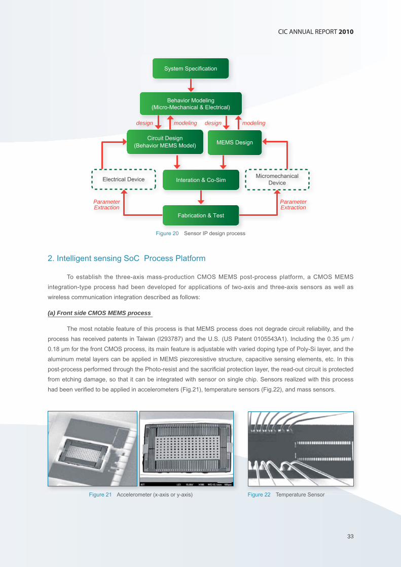
design software to facilitate whole system simulation. Figure 20 shows the sensor IP design process.
Figure 19 Intelligent sensing SoC design platform
Co-Simulation(cadence, hspice, etc.)
SensorIP (SoC)
specification
MEMSSensor &acurator
3D modelgeneration
Materialparemeter
modifications(stress, Young’s
modulus)
Sensorbehavior
simulation
Macromodel
(verilog-A)
Integratedlayout
IC design FlowFull-Custom/Cell-Base/RF IC circuits
MEMS module design flow
33
CIC ANNUAL REPORT 2010
33
2. Intelligent sensing SoC Process Platform
To establish the three-axis mass-production CMOS MEMS post-process platform, a CMOS MEMS
integration-type process had been developed for applications of two-axis and three-axis sensors as well as
wireless communication integration described as follows:
(a) Front side CMOS MEMS process
The most notable feature of this process is that MEMS process does not degrade circuit reliability, and the
process has received patents in Taiwan (I293787) and the U.S. (US Patent 0105543A1). Including the 0.35 μm /
0.18 μm for the front CMOS process, its main feature is adjustable with varied doping type of Poly-Si layer, and the
aluminum metal layers can be applied in MEMS piezoresistive structure, capacitive sensing elements, etc. In this
post-process performed through the Photo-resist and the sacrifi cial protection layer, the read-out circuit is protected
from etching damage, so that it can be integrated with sensor on single chip. Sensors realized with this process
had been verifi ed to be applied in accelerometers (Fig.21), temperature sensors (Fig.22), and mass sensors.
System Specification
Behavior Modeling(Micro-Mechanical & Electrical)
Circuit Design(Behavior MEMS Model) MEMS Design
Interation & Co-Sim
Fabrication & Test
Electrical DeviceMicromechanical
Device
design modeling design modeling
ParameterExtraction
ParameterExtraction
Figure 20 Sensor IP design process
Figure 21 Accelerometer (x-axis or y-axis) Figure 22 Temperature Sensor
3434
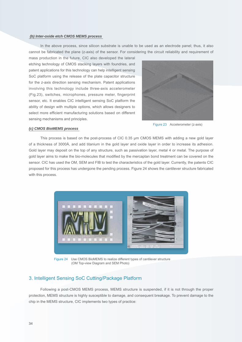
(b) Inter-oxide etch CMOS MEMS process
In the above process, since silicon substrate is unable to be used as an electrode panel; thus, it also
cannot be fabricated the plane (z-axis) of the sensor. For considering the circuit reliability and requirement of
mass production in the future, CIC also developed the lateral
etching technology of CMOS stacking layers with foundries, and
patent applications for this technology can help intelligent sensing
SoC platform using the release of the plate capacitor structure
for the z-axis direction sensing mechanism. Patent applications
involving this technology include three-axis accelerometer
(Fig.23), switches, microphones, pressure meter, fingerprint
sensor, etc. It enables CIC intelligent sensing SoC platform the
ability of design with multiple options, which allows designers to
select more effi cient manufacturing solutions based on different
sensing mechanisms and principles.
(c) CMOS BioMEMS process
This process is based on the post-process of CIC 0.35 μm CMOS MEMS with adding a new gold layer
of a thickness of 3000Å, and add titanium in the gold layer and oxide layer in order to increase its adhesion.
Gold layer may deposit on the top of any structure, such as passivation layer, metal 4 or metal. The purpose of
gold layer aims to make the bio-molecules that modifi ed by the mercaptan bond treatment can be covered on the
sensor. CIC has used the OM, SEM and FIB to test the characteristics of the gold layer. Currently, the patents CIC
proposed for this process has undergone the pending process. Figure 24 shows the cantilever structure fabricated
with this process.
Figure 23 Accelerometer (z-axis)
Figure 24 Use CMOS BioMEMS to realize different types of cantilever structure(OM Top-view Diagram and SEM Photo)
3. Intelligent Sensing SoC Cutting/Package Platform
Following a post-CMOS MEMS process, MEMS structure is suspended, if it is not through the proper
protection, MEMS structure is highly susceptible to damage, and consequent breakage. To prevent damage to the
chip in the MEMS structure, CIC implements two types of practice:

35
CIC ANNUAL REPORT 2010
35
(a) Use photo-resist to protect MEMS structure
In the end of CMOS MEMS process, the MEMS
structure is suspended and it will be directly coated a layer
of Photo-resist in wafer foundry. Photo-resist has a property
of adhesion, as well as certain mobility, which can not only
be fi lled in the hole under MEMS structure, but it is also able
to protect the entire MEMS structure to avoid damage from
follow-up cutting or packaging processes. When designers
got the well-cut chips, they can remove the Photo-resist by
referring to CIC's Photo-resist Removing Process. Figure
25 shows the protection of Photo-resist on chip, and the
condition after removing such Photo-resist. This innovative
method has obtained U.S. patent (US7435663) and Taiwan
patent (I291725) in 2005 and 2007 respectively.
(b) On-wafer measurement
The CMOS MEMS process retains full wafers rather than cutting them. If a structure of the strength is poor,
after coating Photo-resist process after breakage, convenience can use this wafer to do chip MEMS structure of
the measurement. Current approaches could address the MEMS structure damage caused by breakage of the
problem breakage, but this approach is inconvenient when applied to mass production, MEMS structure with poor
strength cannot use Photo-resist protection, so CIC is actively working with package plants to develop Wafer-
Level Package (WLP) technology. Using this technology, MEMS structure in CMOS MEMS process can be used
immediately after the lid is sealed with the future structure, thus achieving protection, MEMS Wafer-Level Package
stability, improved volumes, and improved service time.
4. CMOS G-sensor IP Design Example
Simultaneously with the launch of Wii by Nintendo, Apple introduced the iPhone, and both products
achieved strong sales. Subsequently, the MEMS Inertial Sensorsmarket officially began using MEMS
accelerometer (Accelerometer, G-sensor) to estimate the linear rate of change. Early applications of MEMS
Inertial Sensors focused on the automotive market, including providing impact cushioning protection airbags,
electronic anti-skid systems, etc. Additionally, besides independent applications in hard disk protection, optical
anti- impact devices based on motion-sensing capabilities can be settled via gestures to identify the interface
control mobile devices and game controller, intelligent remote control, 3D mouse, etc., to provide a more intuitive
control interface.
The following uses SoC technology to realize a CMOS G Sensor IP, of which the specifi cations do not stray
far from those of the commercially available ADI G-sensor. Figure 26 illustrates a simple capacitive acceleration
sensor comprising two parts: mechanical structure and read-out circuit. The mechanical structure is part of a
mass block (Mass), spring (Spring) with capacitors (Monitoring Capacitor), where the mass of the block with the
spring is used when the object generates acceleration movement to create the required displacement, while the
interdigital capacitor structure has a different coupling area from the mass of the movement of the block, resulting
in capacitance changes. The main function of the reading circuit is to capture and magnify small changes in
capacitance generated by the interdigitated capacitor volume, and voltage in the form of output for the next level
of the analog / digital converter.
PR coating and dicing After cleaning
Die Level
Figure 25 MEMS structure protected by photo-resist and the chip with photo-resist removed
3636
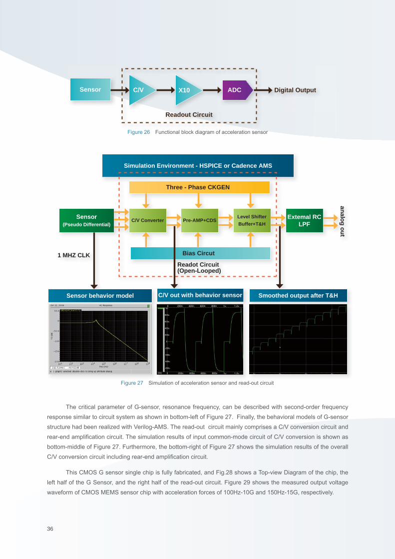
Sensor C/V X10 ADC
Readout Circuit
Digital Output
Figure 26 Functional block diagram of acceleration sensor
Simulation Environment - HSPICE or Cadence AMS
Three - Phase CKGEN
Sensor(Pseudo Differential)
C/V Converter Pre-AMP+CDSLevel Shifter
Buffer+T&HExtemal RC
LPF
Bias Circut
Sensor behavior model C/V out with behavior sensor Smoothed output after T&H
1m
800u
600u
400u
200u
0
-200u
-400u
-600u
-800u
0 200n 400n 600n 800n 1u 1.2u
(lin) 0 200n 400n 600n 800n 1u 1.2u
Readot Circuit(Open-Looped)
1 MHZ CLK
analo
g o
ut
Figure 27 Simulation of acceleration sensor and read-out circuit
The critical parameter of G-sensor, resonance frequency, can be described with second-order frequency
response similar to circuit system as shown in bottom-left of Figure 27. Finally, the behavioral models of G-sensor
structure had been realized with Verilog-AMS. The read-out circuit mainly comprises a C/V conversion circuit and
rear-end amplifi cation circuit. The simulation results of input common-mode circuit of C/V conversion is shown as
bottom-middle of Figure 27. Furthermore, the bottom-right of Figure 27 shows the simulation results of the overall
C/V conversion circuit including rear-end amplifi cation circuit.
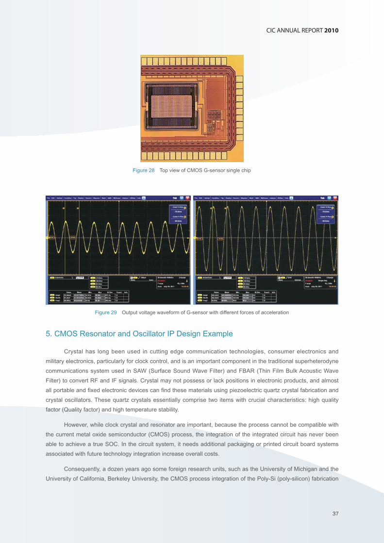
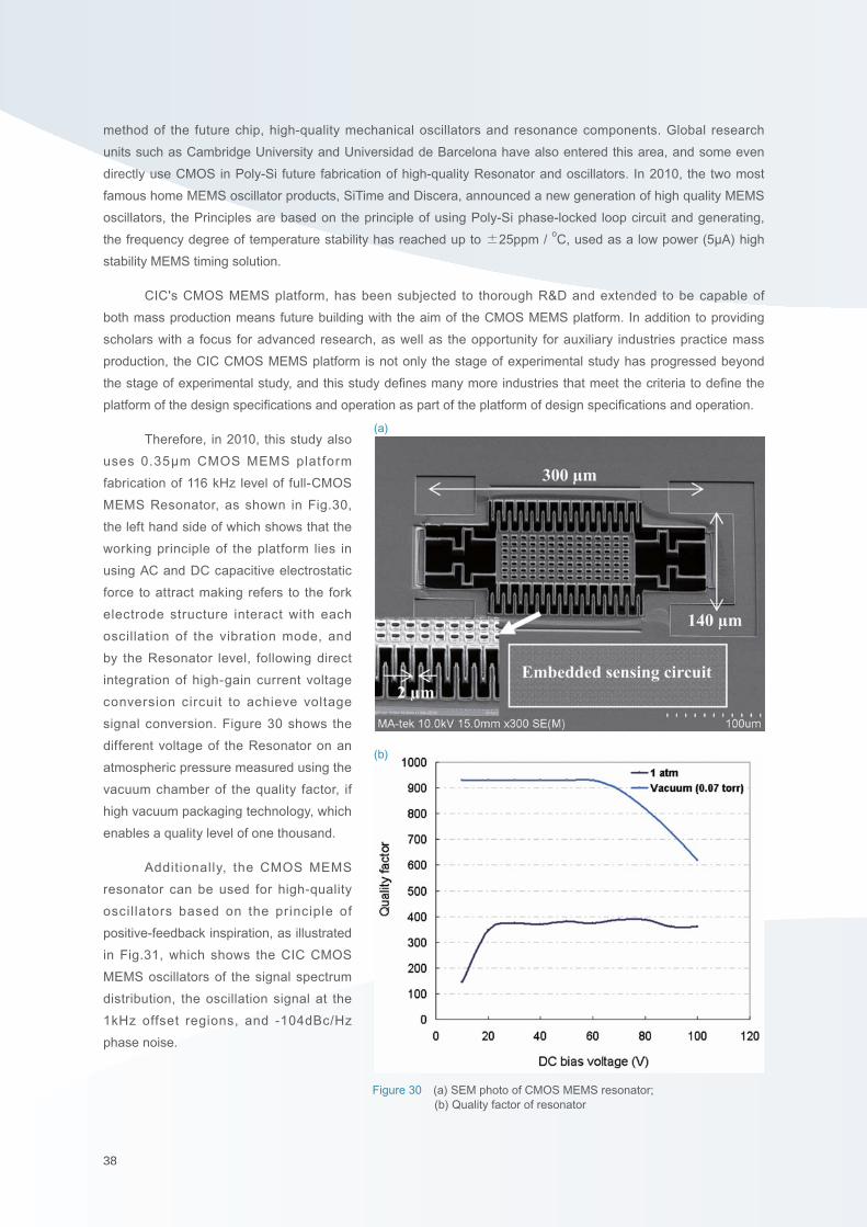
This CMOS G sensor single chip is fully fabricated, and Fig.28 shows a Top-view Diagram of the chip, the
left half of the G Sensor, and the right half of the read-out circuit. Figure 29 shows the measured output voltage
waveform of CMOS MEMS sensor chip with acceleration forces of 100Hz-10G and 150Hz-15G, respectively.
37
CIC ANNUAL REPORT 2010
37
5. CMOS Resonator and Oscillator IP Design Example
Crystal has long been used in cutting edge communication technologies, consumer electronics and
military electronics, particularly for clock control, and is an important component in the traditional superheterodyne
communications system used in SAW (Surface Sound Wave Filter) and FBAR (Thin Film Bulk Acoustic Wave
Filter) to convert RF and IF signals. Crystal may not possess or lack positions in electronic products, and almost
all portable and fi xed electronic devices can fi nd these materials using piezoelectric quartz crystal fabrication and
crystal oscillators. These quartz crystals essentially comprise two items with crucial characteristics: high quality
factor (Quality factor) and high temperature stability.
However, while clock crystal and resonator are important, because the process cannot be compatible with
the current metal oxide semiconductor (CMOS) process, the integration of the integrated circuit has never been
able to achieve a true SOC. In the circuit system, it needs additional packaging or printed circuit board systems
associated with future technology integration increase overall costs.
Consequently, a dozen years ago some foreign research units, such as the University of Michigan and the
University of California, Berkeley University, the CMOS process integration of the Poly-Si (poly-silicon) fabrication
Figure 28 Top view of CMOS G-sensor single chip
Figure 29 Output voltage waveform of G-sensor with different forces of acceleration
3838
method of the future chip, high-quality mechanical oscillators and resonance components. Global research
units such as Cambridge University and Universidad de Barcelona have also entered this area, and some even
directly use CMOS in Poly-Si future fabrication of high-quality Resonator and oscillators. In 2010, the two most
famous home MEMS oscillator products, SiTime and Discera, announced a new generation of high quality MEMS
oscillators, the Principles are based on the principle of using Poly-Si phase-locked loop circuit and generating,
the frequency degree of temperature stability has reached up to ±25ppm / oC, used as a low power (5μA) high
stability MEMS timing solution.
CIC's CMOS MEMS platform, has been subjected to thorough R&D and extended to be capable of
both mass production means future building with the aim of the CMOS MEMS platform. In addition to providing
scholars with a focus for advanced research, as well as the opportunity for auxiliary industries practice mass
production, the CIC CMOS MEMS platform is not only the stage of experimental study has progressed beyond
the stage of experimental study, and this study defi nes many more industries that meet the criteria to defi ne the
platform of the design specifi cations and operation as part of the platform of design specifi cations and operation.
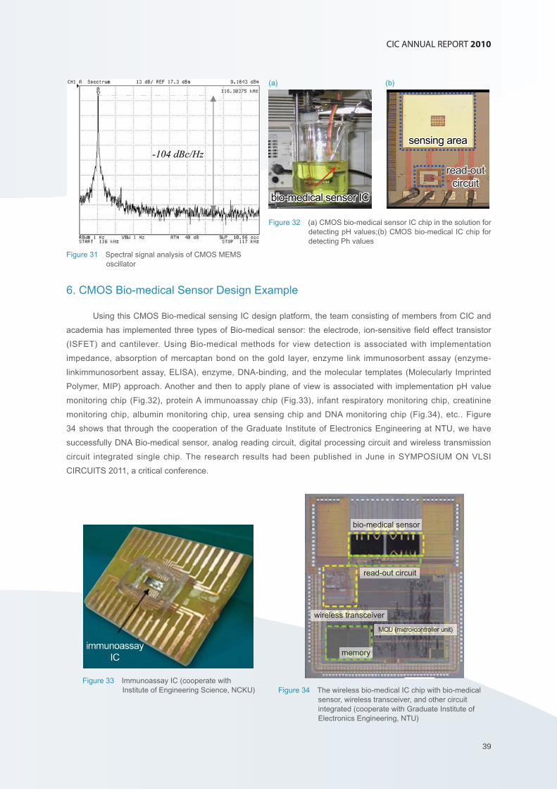
Therefore, in 2010, this study also
uses 0.35μm CMOS MEMS plat form
fabrication of 116 kHz level of full-CMOS
MEMS Resonator, as shown in Fig.30,
the left hand side of which shows that the
working principle of the platform lies in
using AC and DC capacitive electrostatic
force to attract making refers to the fork
electrode structure interact with each
oscillation of the vibration mode, and
by the Resonator level, following direct
integration of high-gain current voltage
conversion circuit to achieve voltage
signal conversion. Figure 30 shows the
different voltage of the Resonator on an
atmospheric pressure measured using the
vacuum chamber of the quality factor, if
high vacuum packaging technology, which
enables a quality level of one thousand.
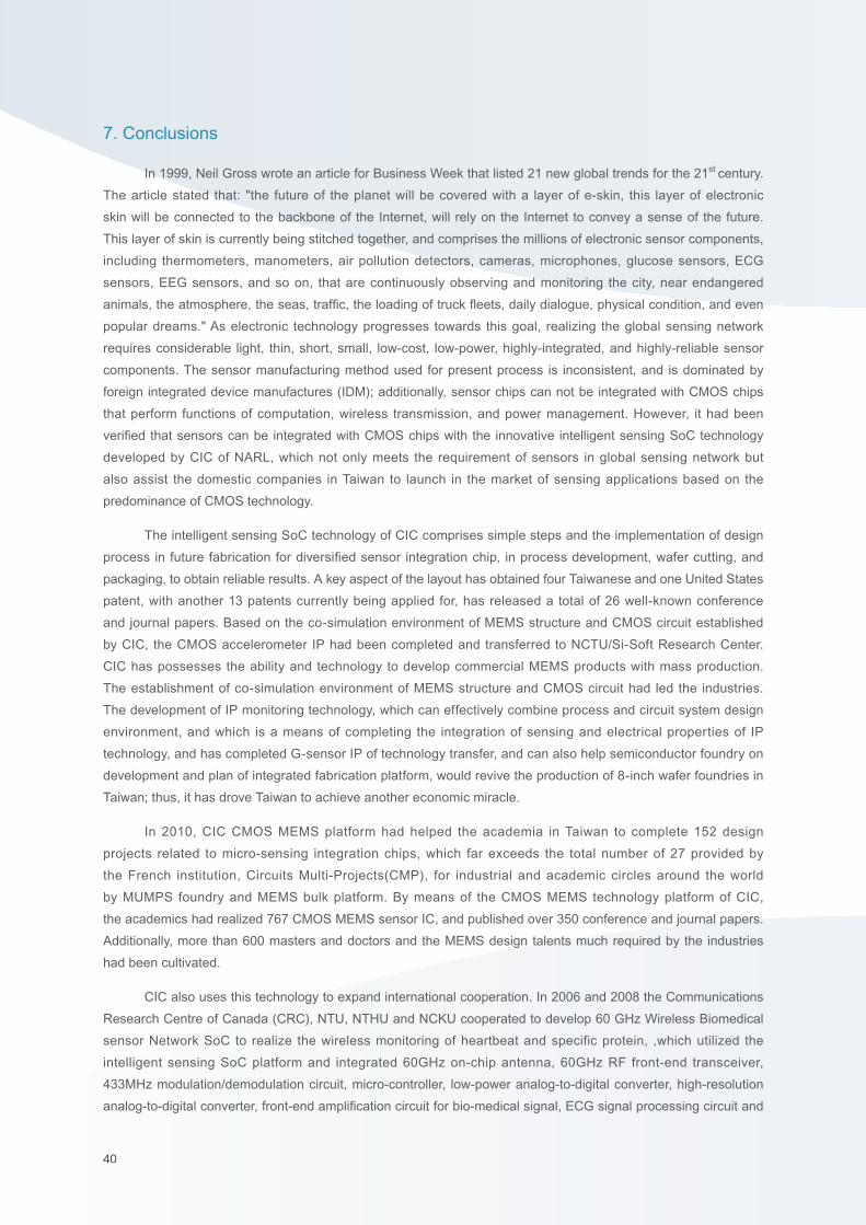
Additionally, the CMOS MEMS
resonator can be used for high-quality
oscil lators based on the principle of
positive-feedback inspiration, as illustrated
in Fig.31, which shows the CIC CMOS
MEMS oscillators of the signal spectrum
distribution, the oscillation signal at the
1kHz offset regions, and -104dBc/Hz
phase noise.
Figure 30 (a) SEM photo of CMOS MEMS resonator; (b) Quality factor of resonator
(a)
(b)
39
CIC ANNUAL REPORT 2010
39
6. CMOS Bio-medical Sensor Design Example
Using this CMOS Bio-medical sensing IC design platform, the team consisting of members from CIC and
academia has implemented three types of Bio-medical sensor: the electrode, ion-sensitive fi eld effect transistor
(ISFET) and cantilever. Using Bio-medical methods for view detection is associated with implementation
impedance, absorption of mercaptan bond on the gold layer, enzyme link immunosorbent assay (enzyme-
linkimmunosorbent assay, ELISA), enzyme, DNA-binding, and the molecular templates (Molecularly Imprinted
Polymer, MIP) approach. Another and then to apply plane of view is associated with implementation pH value
monitoring chip (Fig.32), protein A immunoassay chip (Fig.33), infant respiratory monitoring chip, creatinine
monitoring chip, albumin monitoring chip, urea sensing chip and DNA monitoring chip (Fig.34), etc.. Figure
34 shows that through the cooperation of the Graduate Institute of Electronics Engineering at NTU, we have
successfully DNA Bio-medical sensor, analog reading circuit, digital processing circuit and wireless transmission
circuit integrated single chip. The research results had been published in June in SYMPOSIUM ON VLSI
CIRCUITS 2011, a critical conference.
Figure 31 Spectral signal analysis of CMOS MEMS oscillator
Figure 32 (a) CMOS bio-medical sensor IC chip in the solution for detecting pH values;(b) CMOS bio-medical IC chip for detecting Ph values
(a) (b)
bio-medical sensor
read-out circuit
wireless transceiver
MCU (micro-controller unit)
memory
Figure 33 Immunoassay IC (cooperate with Institute of Engineering Science, NCKU) Figure 34 The wireless bio-medical IC chip with bio-medical
sensor, wireless transceiver, and other circuit integrated (cooperate with Graduate Institute of Electronics Engineering, NTU)
bio-medical sensor ICbio-medical sensor IC
sensing areasensing area
read-outcircuit
read-outcircuit
4040
7. Conclusions
In 1999, Neil Gross wrote an article for Business Week that listed 21 new global trends for the 21st century.
The article stated that: "the future of the planet will be covered with a layer of e-skin, this layer of electronic
skin will be connected to the backbone of the Internet, will rely on the Internet to convey a sense of the future.
This layer of skin is currently being stitched together, and comprises the millions of electronic sensor components,
including thermometers, manometers, air pollution detectors, cameras, microphones, glucose sensors, ECG
sensors, EEG sensors, and so on, that are continuously observing and monitoring the city, near endangered
animals, the atmosphere, the seas, traffi c, the loading of truck fl eets, daily dialogue, physical condition, and even
popular dreams." As electronic technology progresses towards this goal, realizing the global sensing network
requires considerable light, thin, short, small, low-cost, low-power, highly-integrated, and highly-reliable sensor
components. The sensor manufacturing method used for present process is inconsistent, and is dominated by
foreign integrated device manufactures (IDM); additionally, sensor chips can not be integrated with CMOS chips
that perform functions of computation, wireless transmission, and power management. However, it had been
verifi ed that sensors can be integrated with CMOS chips with the innovative intelligent sensing SoC technology
developed by CIC of NARL, which not only meets the requirement of sensors in global sensing network but
also assist the domestic companies in Taiwan to launch in the market of sensing applications based on the
predominance of CMOS technology.
The intelligent sensing SoC technology of CIC comprises simple steps and the implementation of design
process in future fabrication for diversifi ed sensor integration chip, in process development, wafer cutting, and
packaging, to obtain reliable results. A key aspect of the layout has obtained four Taiwanese and one United States
patent, with another 13 patents currently being applied for, has released a total of 26 well-known conference
and journal papers. Based on the co-simulation environment of MEMS structure and CMOS circuit established
by CIC, the CMOS accelerometer IP had been completed and transferred to NCTU/Si-Soft Research Center.
CIC has possesses the ability and technology to develop commercial MEMS products with mass production.
The establishment of co-simulation environment of MEMS structure and CMOS circuit had led the industries.
The development of IP monitoring technology, which can effectively combine process and circuit system design
environment, and which is a means of completing the integration of sensing and electrical properties of IP
technology, and has completed G-sensor IP of technology transfer, and can also help semiconductor foundry on
development and plan of integrated fabrication platform, would revive the production of 8-inch wafer foundries in
Taiwan; thus, it has drove Taiwan to achieve another economic miracle.
In 2010, CIC CMOS MEMS platform had helped the academia in Taiwan to complete 152 design
projects related to micro-sensing integration chips, which far exceeds the total number of 27 provided by
the French institution, Circuits Multi-Projects(CMP), for industrial and academic circles around the world
by MUMPS foundry and MEMS bulk platform. By means of the CMOS MEMS technology platform of CIC,
the academics had realized 767 CMOS MEMS sensor IC, and published over 350 conference and journal papers.
Additionally, more than 600 masters and doctors and the MEMS design talents much required by the industries
had been cultivated.
CIC also uses this technology to expand international cooperation. In 2006 and 2008 the Communications
Research Centre of Canada (CRC), NTU, NTHU and NCKU cooperated to develop 60 GHz Wireless Biomedical
sensor Network SoC to realize the wireless monitoring of heartbeat and specific protein, ,which utilized the
intelligent sensing SoC platform and integrated 60GHz on-chip antenna, 60GHz RF front-end transceiver,
433MHz modulation/demodulation circuit, micro-controller, low-power analog-to-digital converter, high-resolution
analog-to-digital converter, front-end amplifi cation circuit for bio-medical signal, ECG signal processing circuit and
41
CIC ANNUAL REPORT 2010
41
bio-medical micro-sensor. In 2009 the AIBN laboratory of Australia's Queensland University (The University of
Queensland) took the initiative to CIC connected network, hoping to use CIC intelligent sensing SoC technology
platform for future development of Bio-medical related sensor applications. The laboratory is currently working
with NTU and engaged in discussions regarding Bio-medical micro-sensor and circuit chip architecture. In the
future, the laboratory hopes to realize detection of single molecule with nano-electrode, as well as integrate the
bio-medical sensor and its read-out circuit into single chip, the present International Cooperation Department also
intends to promote international co-operation with AIBN. Germany's Freiburg University recently took the initiative
by suggesting the use of the CIC intelligent sensing SoC technology platform for future fabrication of cantilever
in bio-medical related molecule detection. Additionally, CMC in Canada and the president of IMEC chip service
department visited CIC in 2009 and January of 2010, respectively, for introducing this platform to Canada and
Europe, which manifested the achievement and international values of this platform.
Currently, the sensor market is dominated by foreign IDM companies, historically, few Taiwanese
manufacturers dwelt on this sensor market for few or no suitable processes and small number of sensing
applications. The sensor market has become the fastest growing market in the future as sensors are successfully
applied in 3C by Wii and iPhone. The advantages of Taiwan comprises a complete upper, middle and downstream
CMOS IC industrial chain, and the ability to integrate the sensor and IC technology represents the largest profi t
base of industrial development in Taiwan. Through the CMOS sensor platform technology of CIC, academics had
successfully verifi ed the feasibility of integrating CMOS IC with sensors in a single chip. Additionally, in 2009,
CIC cooperated with UMC on a CMOS MEMS process platform suitable for mass production, a project that was
completed this year with the release of a prototype.
Currently several IC design companies had been developing products by means of this platform with
products of CMOS sensors scheduled to be on mass production this year for launching the market of 3C sensor
applications, and will be launched on the 3C sensor application market.
Nature Journal described the global sensing network as likely to become a computer platform in 2020,
which will comprise numerous microcomputers continuously monitoring the ecosystem and buildings of the
earth, as well as the physical conditions of human beings. One National Science Foundation report predicted
that:“Global sensing network will become the first electronic nervous system,”and even forecast that the
global sensing network will initiate the next wave of the computer revolution, following personal computers in the
80s, and the Internet in the 90s. Numerous countries, including Japan, Korea, Canada, etc., have announced
a strong focus on the development of sensor IC, CIC has taken the lead by establishing the intelligent sensing
SoC technology, which can not only assist academics in researching and developing various intelligent sensor
IP, providing IC design and system firms with new horizons, but can also provide IC manufacturers with new
production capability. However, it will drive life-style changes and increase in future well-being.
4242
Patents
CIC pays considerable attention to IP Rights, as to other's IP Rights, CIC has introduced and obtained
from the legal channels and will be well-managed as general IP protection issues, and has helped establish legal
channels for monitoring IP rights. CIC has also enacted various management measures to protect its own IP,
in addition to its general work on managing and protecting the IP of others.
To provide schools with user friendly design software, CIC signs agreements with professors based on
good faith to regulate the scope of authorization (such as only using IP for teaching and research purposes) and
liability. Additionally, CIC uses the license management system to prevent software misues. To date, software
manufacturers are satisfi ed with how individual schools have implemented IP management, and therefore are
providing software to schools at preferential prices.
Title of Approved Patent Country Type Approval Date
A phase-controlled current source for phase-locked loop
Taiwan Invention 2010/4/21
An adapter for the RF front end processor chip U. S. Invention 2010/8/3
Carrier structure of SOC with custom interface
U. S. Invention 2010/7/13
Edge-missing detector structure U. S. Invention 2010/12/28
Title of Pending Patent Country TypeDate of
Application
Method for manufacturing 4-axial monitoring MEMS device on compatible CMOS platform
U. S. Invention 2010/1/5
Hydrogen ion sensitive fi eld effect transistor and manufacturing method thereof
Taiwan Invention 2010/1/11
Hydrogen ion sensitive fi eld effect transistor and manufacturing method thereof
U. S. Invention 2010/3/16
CMOS-MEMS cantilever structure U. S. Invention 2010/2/19
Multi layer system chip module architectures U. S. Invention 2010/1/12
Method for arranging memories of low-complexity ldpcdecoder and low-complexity ldpcdecoder using the same
U. S. Invention 2010/2/18
Table 4 2010 Patent Approved and Application List
43
CIC ANNUAL REPORT 2010
43
Three-dimensional SoC structure stacking by multiple chip modules
Taiwan Invention 2010/1/29
Three-dimensional SoC structure stacking by multiple chip modules
U. S. Invention 2010/4/1
Unitized charging and discharging battery management system and programmable battery management module thereof
Taiwan Invention 2010/1/22
Unitized charging and discharging battery management system and programmable battery management module thereof
U. S. Invention 2010/3/22
Device including a virtual drive system Taiwan Invention 2010/5/12
Device including a virtual drive system U. S. Invention 2010/6/23
Virtualized peripheral hardware platform system Taiwan Invention 2010/10/22
Virtualized peripheral hardware platform system U. S. Invention 2010/12/7
Year 2006 2007 2008 2009 2010
Cases Approved 0 1 4 2 4
Cases Applied 5 5 6 10 14
Table 5 Patents Approved and Applied Table
4444
Papers
2010 Theses in International Journal (Journal Papers)
1. C. L. Wei, C. F. Lin, and I. T. Tseng,“A novel MEMS respiratory fl ow sensor,”IEEE Sensors Journal, vol. 10,
no. 1, January 2010, pages 16-18.
2. Hann-Huei Tsai, Chen-Fu Lin, Ying-Zong Juang, I-Long Wang, Yu-Cheng Lin, Ruey-Lue Wang, and Hung-Yin
Lin,“Multiple type biosensors fabricated using the CMOS BioMEMS platform,”Sensors and Actuators, B,
Volume 144, Issue 2, February 2010, pages 407-412.
3. Chien-Hsuan Liu, Yan-Kuin Su, Ruey-Lue Wang, Chih-Ho Tu, and Ying-Zong Juang,“The Layout Geometry
and Power-level Dependences of Degradation in CMOS RF Power Cells from Hot-carrier Stress with Load Pull
system,”Japanese Journal of Applied Physics, vol. 49, no. 4, April 2010, pages 04DC27-1~04DC27-3.
4. HAROUN Ibrahim, WIGHT Jim, PLETT Calvin, FATHY Aly, and CHANG Da-Chiang,“Experimental Analysis
of a 60 GHz Compact EC-CPW Branch-Line Coupler for mm-Wave CMOS Radios,”IEEE microwave and
wireless components letters, vol. 20, no. 4, April 2010, pages 211-213.
5. Chien-Hsuan Liu, Yan-Kuin Su, Ruey-Lue Wang, Chih-Ho Tu, and Ying-Zong Juang,“DC and RF Degradation
Induced by High RF Power Stresses in 0.18μm nMOSFETs,”IEEE Transactions on Device and Materials
Reliability (T-DMR), vol. 10, no. 3, September 2010, pages 317-323.
6. Ruey-Lue Wang, Chien-Hsuan Liu, Yan-Kuin Su, Chih-Ho Tu, and Ying-Zong Juang,“The Layout Geometry
Dependence of the OMIT? Power Cells on Performances and Reliability,”IEEE Microwave and Wireless
Components Letters, vol. 20, no. 12, December 2010, pages 687-689.
7. Chun-Ming Huang, Chien-Ming Wu, Chih-Chyau Yang, Shih-Lun Chen, Chi-Shi Chen, Jiann-Jenn Wang, Kuen-
Jong Lee, and Chin-Long Wey,“Programmable system-on-Chip (SoC) for Silicon Prototyping,”accepted for
publication by IEEE Transaction on Industrial Electronics.
8. Chun-Ming Huang, Yu-Tsang Chang, Ju-Yun Hsieh, Chien-Ming Wu, Chen-Yen Lin, Hsi-Tse Wu, Wei-De Chien,
and Chin-Long Wey,“A Modularized FPGA Development Platform for IC Design Education,”Innovations
2010: World Innovations in Engineering Education and Research, W. Aung et al. (eds. ), iNEER, pp. 197-212,
2010.
9. Shyue-Kung Lu, Chun-Lin Yang, Yuang-Cheng Hsiao, and Cheng-Wen Wu,“Effi cient BISR Techniques for
Embedded Memories Considering Cluster Faults,”IEEE Transactions on Very Large Scale Integration (VLSI)
systems, vol. 18, no. 2, pp. 184-193, February 2010.
10. Robert Chen-Hao Chang, Chih-Hung Lin, Kuang-Hao Lin, Chien-Lin Huang, and Feng-Chi Chen,“Iterative
QR Decomposition Architecture Using the Modified Gram-Schmidt Algorithm for MIMO-OFDM systems,”
IEEE Transactions on Circuits and systems I, vol. 57, pp. 1095-1102, MAY 2010
45
CIC ANNUAL REPORT 2010
45
2010 Theses in International Conference (Conference Papers)
1. Ting-Hsu Chien, Chi-Sheng Lin, Chin-Long Wey, Ying-Zong Juang, and Chun-Ming Huang,“HIGH-SPEED
AND LOW POWER PROGRAMMABLE FREQUENCY DIVIDER,”Proc. Int. Symp. NOTE Could you write out
in full? Circuits and systems, Paris, France, May 30th-June 2
nd, 2010.
2. You-Liang Lai, Ying-Zong Juang, Sheng-Chieh Huang, Sheng-Hsiang Tseng, and Hann-Huei Tsai,“Effective
Mechanical Properties Measurement in Standard IC CMOS process,”5th
Asia-Pacific Conference on
Transducers and Micro-Nano Technology, Perth, Australia, Jul. 6th-Jul. 9th, 2010.
3. Zhen-Yu Li, Herming Chiueh, Ying-Zong Juang, and Chin-Fong Chiu,“A Small Area Fully Integrated Spread-
Spectrum Clock Generator with High EMI-reduction for SATA-3.0 applications, 53rd
IEEE International Midwest
Symposium on Circuits and Systems, Seattle, U.S.A. , Aug. 1st 2010-Aug. 4
th, 2010
4. S.-H. Tseng, Michael S. -C. Lu, Y. -J. Hung, Y. -Z. Juang,“High-Q CMOS MEMS Resonator Oscillator
Fabricated in a MPW Batch Process,”Linz, Austria, Eurosensors Sep. 5th 2010-Sep. 8
th, 2010.
5. Yin-Cheng Chang, Shuw-Guann Lin, Hwann-Kaeo Chiou, Da-Chiang Chang, and Ying-Zong Juang,
“On-Wafer Noise Figure Measurements of Millimeter-Wave LNA and Mixer,”IEEE Asia-Pacifi c Microwave
Conference, Yokohama, Japan, Dec. 7th-10
th, 2010.
6. Hsu-Feng Hsiao, Shuw-Guann Lin, Hwann-Kaeo Chiou, Da-Chiang Chang, and Ying-Zong Juang,
“On-Wafer mm-Wave V-band Semi-Automatic Power Measurement system,”Asia-Pacific Microwave
Conference, Yokohama, Japan, December 7-10, 2010
7. Yuan-Ta Hsieh, Bin-Da Liu, Jian-Fu Wu, Chiao-Li Fang, Hann-Huei Tsai, and Ying-Zong Juang,“A High
Effi ciency Boost White LED Driver for Portable Electronics Applications,”International Symposium on Next-
Generation Electronics, Kaohsiung, Taiwan, November 18-19, 2010.
8. Yuan-Ta Hsieh, Bin-Da Liu, Jian-Fu Wu, Chiao-Li Fang, Hann-Huei Tsai, and Ying-Zong Juang,“A High
Effi ciency Boost White LED Driver with Integrated Schottky Diode,”2010 Asia Pacifi c Conference on Circuits
and systems (APCCAS 2010) 6-9 December 2010, Kuala Lumpur, Malaysia.
9. Chi-Sheng Lin, Ting-Hsu Chien, Chun-Ming Huang, Ing-Zong Juang, and Chin-Long Wey,“DESIGN OF A
HIGH-SPEED AND LOW-POWER PROGRAMMABLE FREQUENCY DIVIDER,”IEEE ISCAS, pp. 1843-1846,
May 2010.
10. Ting-Hsu Chien, Chi-Sheng Lin, and Chin-Long Wey,“High-Speed and Low-Power Programmable Frequency
Divider,”IEEE ISCAS, pp. 4301-4304, May 2010.
11. Chih-Hsing Lin, Yung-Chang Chang, Wen-Chih Huang, Wei-Chih Lai, Ching-Te Chiu, Jen-Ming Wu, Shuo-
Hung Hsu, Chun-Ming Huang, Chih-Chyau Yang, and Shih-Lun Chen,“A Packet-based Emulating Platform
with Serializer/Deserializer Interface for Heterogeneous IP Verifi cation,”IEEE ISCAS, pp. 1061-1064, May
2010.
4646
12. Hsin-Fu Luo, Ming-Der Shieh, Yi-Jun Liu, and Chien-Ming Wu,“Efficient Memory Management for FFT
processors,”IEEE ISCAS, pp. 3737-3740, May 2010.
13. Kai-Chao Yang, Chun-Lung Lin, Tung-Lin Wu, and Jia-Shung Wang, "Service-Driven Approximate LT Codes,"
IEEE ICC, pp. 1-5, May 2010.
14. Kai-Chao Yang, Chih-Ting Kuo, Yu-Tsang Chang, Chien-Ming Wu, Jia-Rong Chang, Chun-Ming Huang,
and Chin-Long Wey,“Case Study: A Universal Study Platform for Embedded Software Education,”ICEE, pp.
1-8, Aug. 2010.
15. Chih-Chyau Yang, Chen-Yen Lin, Hui-Ming Lin, Yui-Chih Shih, His-Tse Wu, Shi-Lun Chen, Tien-Ching Wang,
Chien-Ming Wu, Chun-Ming Huang, and Chin-Long Wey,“Concord: A Configurable SoC Prototyping
Platform,”Sasimi, pp. 31-36, 2010.
16. Yu-Tsang Chang, Chun-Ming Huang, Chien-Ming Wu, Chun-Yu Chen, Yu-Sheng Lin, Chih-Ting Kuo,
Ting-Chun Liu, and Chin-Long Wey,“A Modularized FPGA-Based Embedded system Development
Platform,” IEEE IECON, pp. 1691-1696, Nov. 2010.
17. Yu-Tsang Chang, Chun-Ming Huang, Chien-Ming Wu, Chun-Yu Chen, Yu-Sheng Lin, Chih-Ting Kuo,
Ting-Chun Liu, and Chin-Long Wey,“MorFPGA: A Modularized FPGA-Based Embedded system Development
Platform,”SASIMI, pp. 64-69, Oct. 2010.
18. Wen-Ching Lin, Ming-Der Shieh, and Chien-Ming Wu,“Design of High-Speed Bit-Serial Divider in GF(2m),”
IEEE ISCAS, pp. 713-716, May 2010.
19. Yung-Keui Lu, Ming-Der Shieh, and Chien-Ming Wu,“Low-Complexity Reed-Solomon Decoder for Optical
Communications,”IEEE ISCAS, pp. 4173 - 4176, May 2010.
20. Alex Chien-lin Huang, Robert Chen-Hao Chang, and Chih-Hung Lin,“Low-Power Design of Variable
Block-Size LDPC Decoder Using Nanometer Technology,”IEEE ISCAS, pp. 1759-1762, May 2010.
21. Kai-Chao Yang, Yuan-Cheng Yang, and Jia-Shung Wang,“Hierarchical Data Management for
Spatial-Temporal Information in WSNs,”SENSORCOMM, pp. 435-440, Jul. 2010.
22. Chuan-Yu Cho, Yu-Hung Hsiao, Jia-Shung Wang, and Kai-Chao Yang,“Data Aggregation with Spatially
Correlated Grouping Technique on Cluster-based WSNs,”SENSORCOMM, pp. 584-589, Jul. 2010.
23. Chun-Lung Lin, Kai-Chao Yang, Chuan-Yu Cho, Jia-Shung Wang, and Hsin-Hua Lee,“Optimal Rate Allocation
for Gathering Correlated Data with Distortion Guarantee in sensor Networks,”SENSORCOMM, pp. 428-434,
2010.
24. Chi-Sheng Lin, Ting-Hsu Chien, and Chin-Long Wey,“An OMIT? Effective Phase Detector for Phase-Locked
Loops with Wide Capture Range and Fast Acquisition Time,”Proc. Int. Symp. NOTE Can you write out in full?
Circuits and systems (ISCAS 2010).
47
CIC ANNUAL REPORT 2010
47
2010 Theses in Domestic Conference
1. Ruey-Lue Wang, Chen-Fu Lin, Chiao-Li Fang, Po Cheng Kung, Chiung-Min Yeh, Hsien-Wen Chang, Po-Chang
Wu, Hann-Huei Tsai, Ying-Zong Juang, and Yan-Kuin Su,“A pH-ISFET integrated with a read-out oscillation
circuit for pH value detection,”21st VLSI CAD, Kaohsiung, Taiwan, Aug. 3 2010-Aug. 6 2010.
2. Chen-Yen Lin, Chih-Chyau Yang, Hui-Ming Lin, Yui-Chih Shih, His-Tse Wu, Shi-Lun Chen, Tien-Ching Wang,
Chien-Ming Wu, Chun-Ming Huang, and Chin-Long Wey,“A Fully Confi gurable SoC Prototyping Platform,”
VLSI/CAD Symposium, 2010.
3. Chih-Hsing Lin, Yung-Chang Chang, Wen-Chih Huang, Wei-Chih Lai, Ching-Te Chiu, Jen-Ming Wu,
Shuo-Hung Hsu, Chun-Ming Huang, Chih-Chyau Yang, and Shih-Lun Chen,“A Packet-based Emulating
Platform with Serializer/Deserializer Interface for Heterogeneous IP Verifi cation,”VLSI/CAD Symposium, 2010.
4. Chun-Yu Chen, Yu-Shen Lin, Chi-Ting Kuo, Yu-Chan Chang, Chien-Ming Wu, Chun-Ming Huang,
Chien-Chen Wang, and Chin-Long Wey,“MorFPGA: FPGA-based Modularization Embedded System
Development Platform,”CIASPCD, pp. 275-280, Oct. 2010. (ISBN: 978-986-6212-06-02)

4848

49
CIC ANNUAL REPORT 2010
49
CIC ANNUAL REPORT 2010
5050
(1) Chip and system Design Implementation Environment
To assist domestic academic circles in researching chip and system; over the years, CIC has introduced
various popular design testing software, and has integrated and packed that software to provide free applications
for teachers and students. Recently, together with demand for improvements in process technique and SoC
design, individual EDA companies have continually updated their old design testing software and functions,
as well as launching the latest design testing techniques and software. CIC has also negotiated with well-known
domestic and foreign EDA companies to update various design testing softwares, and to re-integrate various
design fl ows to provide each school for further using purpose.
In 2010, CIC provided design implementation software to the following 19 well-known companies: Altera,
Altos, Agilent, Ansoft, ARM, Cadence, CoWare, Carbon, Dolphin Integration, Magma, Mentor Graphics, National
Instrument, SpringSoft, Synopsys, Syntest, TinnoTek, TI, TransEDA and Xilinx.
As for updating the design environment (Tables 6 and 7), in line with demand for multi-voltage design
low-power circuit, CIC introduced Altos liberate, for establishing design database at different voltages under the
property model, and TinnoTek PowerMixer, for faster calculation of power addition, to improve design environment
usage effi ciency, and eliminate Magma blaster and talus.
Design Environment Services
Company Name Software
1 Altos liberate
2 TennoTek PowerMixer
Table 6 Introduced Software by CIC in 2010
Company Name Software
1 Magma blaster, talus
Table 7 Eliminated Software by CIC in 2010
In the design library area, in 2010 CIC updated design database Artisan TSMC 0.18μm CMOS Cell library,
Faraday UMC 90nm CMOS Cell library and ARM TSMC 90nm CMOS Cell library and introduced ARM TSMC
130nm CMOS Cell library for mixed-signal IC design use.
In terms of Silicon IP Database and ESL System Level Virtual Platform (Tables 8 and 9), CIC introduced
Andes N1213-30T2G Processor Hard IP (TSMC 90nm process) and N903-FGT-C6 Processor Firm IP in 2010,
making them available within academic circles free of charge; additionally, CIC has introduced ITRI through the
PAC digital processor Soft IP and PAC DUO ESL system Level Virtual Platform, has purchased the current case
51
CIC ANNUAL REPORT 2010
51
acceptance, pending completion of related documentation by CIC, and technical information collated will be
provided to academic circles as soon as possible for free use.
To sum up the above updates, in 2010, CIC also updated and conserved related design process and
environment for seven types of chips and systems: Electronic system Level (ESL), Cell-based IC, Platform-based
SoC, Full-Custom IC, FPGA, Mixed-Signal IC and IC Testing.
Company Name Silicon IP database Name
1 Andes N1213-30T2G Processor Hard IP
2 Andes N903-FGT-C6 Processor Firm IP
3 ITRI PAC Digital Processor Soft IP
Table 8 Silicon IP database introduced by CIC in 2010
Company NameSystem Level Virtual
Platform Name
1 ITRI PAC DUO ESL system Level Virtual Platform
Table 9 system Level Virtual Platform introdced by CIC in 2010
(2)Embedded system Design Implementation Environment
Embedded system design is an important key technology that is mainly used to promote SoC design.
Since 2006, to satisfy demand for developing embedded system and assist academia in engaging in research and
teaching related to, CIC started to establish an excellent embedded system design environment and technology,
and introduced and integrated software and hardware facilities of research projects related to the embedded
system to provide teachers and students of each school for further utilization of research. Additionally, within the
research environment and technologies established by full-time researchers from CIC, training courses were
opened to graduate students of each school in embedded system design. In 2010, to coordinate with the NSC
commissioned projects, CIC used its『domestically self-developed』embedded system platform as a basis and
introduced three different types of domestically self-developed embedded system platforms: (1) SunPlus S+Core-
SPCE3200 hardware platform (S+Core-7) introduced 31 sets (platform as shown in Fig.35 (a)); (2) ANDES
Leopard hardware platform (AndesCore N1213) introduced 39 sets (platform as shown in Fig.35 (b)); (3)ITRI
PAC-PMP hardware platform (PAC digital processing core) introduced 32 sets (platform as shown in Fig.35 (c)).
Simultaneously, CIC has also assisted 23 professors who participated in the application of『NSC embedded
system development project』in building embedded system lab, and provided them with related technology
consulting. Moreover, the platform BSP and related documentation of these three companies have also been
5252
updated and uploaded to the offi cial CIC website for downloading and use by school professors and students,
where the relevant website is as follows: (http://www.cic.org.tw/cic_v13/dsd/dsdsoftq01.jsp?ListType=Vender).
(a) Sunplus S+Core-SPCE3200 Embedded Development Hardware Platform PCB (S+Core-7)
(b) Andes ANDES Leopard Embedded Development Hardware Platform PCB (AndesCore N1213)
(c) ITRI PAC-Solo PMP Duo-core Embedded Development Hardware Platform PCB (PAC digital processor core)
Figure 35 Embedded System Platform Intorduced in 2010
Additionally, to establish the software and hardware environment, together with demand from training courses
and academic research, CIC has built the reference design for the embedded system, and coordinated with NSC on
project commissioning. In 2010, CIC completed three embedded software reference designs, as follows:
● Embedded software developed using the domestic Sunplus SPCE3200 platform (a digital photoframe
provides an example)
● Embedded software developed using the Andes ESL virtual platform (the domestic Andes platform provides
an example)
● Embedded software developed using the domestic ITRI PAC-Duo platform DVFS with low power-consumption
53
CIC ANNUAL REPORT 2010
53
Additionally, to promote the embedded system design and attract more students to participate in embedded
system design, in 2010 CIC has worked under the National Science Council to organize ten training courses
related to embedded software design. Table 10 lists details of these sessions. Besides these training courses, CIC
has also worked with industrial and academic circles to organize embedded software related workshops. In 2010,
CIC held eight workshops, as listed in Table 11.
Start Date Course TitleLecturer Service
UnitDays
Instruction Hour
Jan. 18, 2010 Embedded software design with Sunplus platform
CIC 1 8
Jan. 21, 2010Embedded software design with ANDES platform
CIC 2 16
Feb. 2, 2010 Embedded system: bare-level bootloader design concept and implementation
CIC 2 16
Feb. 3, 2010 ARM Processor Design Kit CIC 3 24
Feb. 4, 2010Brief Introduction and Use of ITRI PAC-Duo Hardware Platform
ITRI 2 16
Feb. 22, 2010 system-Level Design with Platform Architect CIC 2 16
Feb. 24, 2010 system-Level Design with SoC Designer CIC 2 16
Mar. 8, 2010Brief Introduction and Use of ITRI PAC-Duo hardware platform
ITRI 2 16
Jun. 10, 2010Brief Introduction and Use Training Course of ITRI PAC-Duo Hardware Platform
ITRI 2 16
Jun. 28, 2010Andes Training Course of AndesShape Duo-core Embedded Platform
Andes 1 8
Table 10 Courses related to Embedded Software Desgin
5454
Start Date Course TitleLecturer Service
UnitDays
Instruction Hour
Jan. 25, 2010 Local Embedded system Platform Workshop
Dept. of Information
Engineering, KSU3 24
Mar. 27, 2010Embedded Development Testing Solution Workshop (central session)
Sunplus 1 8
Apr. 29, 2010Embedded Development Testing Solution Workshop (Taipei session)
Sunplus 1 8
Jul. 3, 2010 Local platform seed teacher and assistant instructor training workshop (Andes, Android)
NCCU 2 16
Jul. 10, 2010 Local platform seed teacher and assistant instructor training workshop (Andes, Android)
NCCU 2 16
Jul. 17, 2010Local platform seed teacher and assistant instructor training workshop(Andes, Android)
NCCU 2 16
Aug. 9, 2010 Local platform seed teacher and assistant instructor training workshop(Sunplus)
NCCU 2 16
Aug. 16, 2010Local platform seed teacher and assistant instructor training workshop (Sunplus)
NCCU 2 16
Table 11 Embedded Software Related Workshop
Regarding the embedded software design contests, Code-O-Rama design competitions have been
organized since 1995, and over the years have seen students produce numerous creative and practical designs.
The competition held this year saw 106 groups drawn from elite tertiary institutions in Taiwan produce entries
based on the theme:“Smart Idea. Smarter Life.”The hope of such competitions is that they will stimulate
students to imagine the future of intelligent life based on the works of previous years. Students participate in such
competitions not only to devise creative designs using ARM architecture, but also to identify future possibilities
related to intelligent life that are creative, technological, convenient, and have high integrity.
(3) MorFPGA: Modularization FPGA Teaching & Contest common Platform
The MorFPGA platform was completed in April 2008, and is the result of R & D conducted by CIC on the
first modularization FPGA teaching-cum-competition common platform. During 2008 to 2010, the Ministry of
Education organized the adoption of the MorFPGA platform IC design contest and also resolved the fairness of
the game problem. The 2008 exam was the fi rst to be used without amendments, members of the direct use of
the subject when the topic questions, that this platform can solve a problem can not be diversifi ed over the years.
According to those content results from 2008 to 2010, this platform can enhance discrimination rate in games.
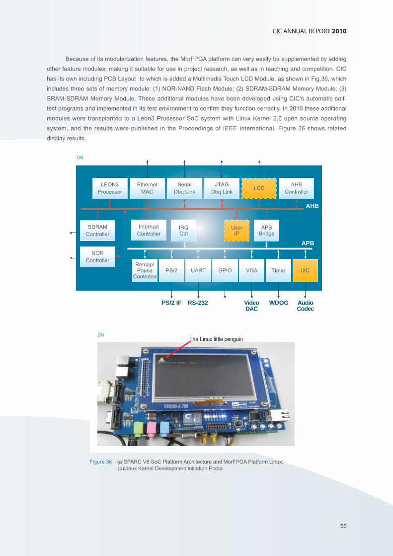
55
CIC ANNUAL REPORT 2010
55
Because of its modularization features, the MorFPGA platform can very easily be supplemented by adding
other feature modules, making it suitable for use in project research, as well as in teaching and competition. CIC
has its own including PCB Layout to which is added a Multimedia Touch LCD Module, as shown in Fig.36, which
includes three sets of memory module: (1) NOR-NAND Flash Module; (2) SDRAM-SDRAM Memory Module; (3)
SRAM-SDRAM Memory Module. These additional modules have been developed using CIC's automatic self-
test programs and implemented in its test environment to confi rm they function correctly. In 2010 these additional
modules were transplanted to a Leon3 Processor SoC system with Linux Kernel 2.6 open source operating
system, and the results were published in the Proceedings of IEEE International. Figure 36 shows related
display results.
LEON3Processor
AHB
EthernetMAC
SerialDbq Link
JTAGDbq Link
LCDAHB
Controller
SDRAMController
NORController
InterruptController
Remap/Pause
ControllerPS/2 UART GPIO VGA Timer I2C
IRQCtrl
APBBridge
UserIP
APB
PS/2 IF RS-232 VideoDAC
WDOG AudioCodec
(a)
(b)
Figure 36 (a)SPARC V8 SoC Platform Architecture and MorFPGA Platform Linux; (b)Linux Kernel Development Initiation Photo

5656
Additionally, to support competition outside of IC, this platform will also allow for the CIC training course
to be offered over the summer vacation. So far, the course has been offered over eight sessions, and is the fi rst
self-made platform to be used in the training course of CIC (the purchaser of commercially available platform
previously used the FPGA platform). In the FPGA platform, CIC only supported a single platform, reducing labor
costs, and avoiding supporting the concerns of particular vendors.
Since MorFPGA platform is the only platform in the world that can integrate with FPGA modules from
leading global manufacturers, such as Altera and Xilinx, and since it also possessed the characteristics of
“modulization,”in 2010 many professors expressed interest in purchasing this platform; to date more than 24
professors from six departments and institutes from 19 colleges and universities wish to purchase the MorFPGA
platform; additionally, many professors from foreign schools have mailed CIC requesting to purchase this platform.
The MorFPGA platform is the fi rst commercialized R&D result of CIC. The platform achieved good sales in 2009
and 2010, including sales to 19 universities, six departments, and 24 professors.
A total of 78 sets of the platform were sold, earning income of approximately NTD 2,089,780. Proceeds to
date from the sale and rental of the MorFPGA platform total approximately NTD 3,500,000.
(4) IC design and Manufacturing Service
Back-end realization of digital chip is a detailed and complicated task since it requires simultaneously
considering problems of chronological order, power source and process rule. Owing to the diffi culty academic
research teams face in obtaining feedback regarding the design of advanced process digital chip with high
complexity and SIP, academics hope for assistance from CIC. Therefore, at the end of 2010, CIC begun to assess
the feasibility of the RTL Sigh-off design service, and hopes to use the ample experience of CIC engineers in
IC design and verification, in addition to stable and reliable methods, so the Advanced Research Team can
implement RTL design practice as the chip to increase the tape out success rate for the advanced process digital
chip with high complexity and SIP. Additionally, compared with the design ability of students, given the abundant
practical experience of CIC engineers, they can also minimize the chip size and increase chip efficiency, and
furthermore can reduce the cost of advanced chip manufacture processes. Moreover, the quality of theses input
from CIC engineers can also help increase the quality of theses written by students. Proceeding methods of
this service will be students only need to complete their RTL design and confi rm that it can be synthesized and
functions correctly, after which they can submit it to CIC to complete back-end fabrication, including automatic
layout and routing, DRC and LVS verifi cation, etc. Figure 37 shows the service fl ow.
To further test the process of IC design service, in addition to implementing the design environment for the
MorPACK R&D project; since the end of 2010, CIC has invited six domestic research groups to cooperate to test
the design environment. These groups include the team of Prof. An-Yu Wu of National Taiwan University; the team
of Prof. Yin-Tsun Hwang of National Chung Hsing University; the team of Prof. Cheng-Yi Lee of National Chiao
Tung University; the team of Prof. Chu-Yin Kuo of NCCU; the team of Prof. Kun-Chung Lee of National Cheng
Kung University; and the team of Ming-Hua Hsu of National Yunlin Science and Technology University. The 90nm
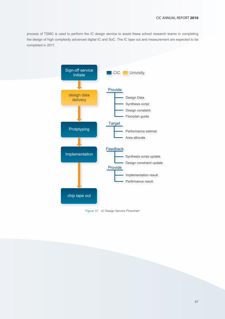
57
CIC ANNUAL REPORT 2010
57
process of TSMC is used to perform the IC design service to assist these school research teams in completing
the design of high complexity advanced digital IC and SoC. The IC tape out and measurement are expected to be
completed in 2011.
chip tape out
Implementation
Protptyping
design data delivery
Sign-off service Initiate
CIC Univisity
Provide
Design Data
Synthesis script
Design constaint
Floorplan guide
Target
Performance estimat
Area allocate
Feedback
Synthesis script update
Design constraint update
Provide
Implementation result
Perfirmance result
Figure 37 IC Design Service Flowchart
5858
Processes for Prototyping IC Fabrication
In 2010, CIC continued on completing 11 process environments, as well as the provision of real-time
information updates, including 4 CMOS processes, 2 BiCMOS processes, 1 GaAs process, 2 CMOS MEMS
processes, 1 CMOS BioMEMS process, and 1 high -voltage process, as follows:
■ UMC 90nm MS CMOS
■ TSMC 90nm MS/RF CMOS
■ TSMC 0.18μm 1P6M CMOS
■ TSMC 0.35μm 2P4M CMOS
■ TSMC 0.35μm SiGe BiCMOS
■ TSMC 0.18μm 3P6M SiGe BiCMOS
■ WIN 0.15μm PHEMT GaAs
■ TSMC 0.35μm CMOS MEMS
■ TSMC 0.18μm CMOS MEMS
■ TSMC 0.35μm CMOS BioMEMS
■ TSMC 0.25μm 60V High Voltage
The process environment that CIC had introduced and built functions to integrate technical data relevant
to processes including Process Design Kit, Design Rule, and Model File, etc. Furthermore, in order to confi rm
the feasibility of utilizing the technical data in EDA environment, CIC verify the compatibility of EDA environment
through real circuit. For easy application of using the environment, all the verifi ed environment and data about
processes can be downloaded from the website of CIC by professors. In addition, CIC also provided the relevant
training courses to facilitate the academics to design circuit with the process environment. Additionally, CIC also
has related training courses, and assisted school professors and students familiar with process environment in
circuit design. During 2010 CIC continued to expand related technical information and FAQ services, and also
established design examples.
The academics in Taiwan had published 729 papers (including 3 ISSCC papers) by using the environment
of advanced processes provided by CIC. The total amount of papers will be increased by ten after registration of
the fi rst quarter of 2011. In 2010, the advanced and educational chips taped out by the academics via CIC had
reached a total amount of 1718 including 1421 advanced chips with relevant production of 0.513 papers per chip.
In respect to the introduction and development of advanced processes, CIC continued to analyze the
development progress of advanced processes with the critical goal of introducing advanced processes for
the requirement of circuit design with advancement of process technology. In 2010, CIC had introduced and
developed the relevant processes as follows:
Chip Implementation Services
59
CIC ANNUAL REPORT 2010
59
■ Completed evaluation and introduction of the Global Foundries 40nm process. A comparison was made with
processing fi rms to provide the integrity of process options and design environment to advance implementation
of the 40nm Low Power process environment, and had completed the Full-Customer IC design environment.
■ Completed evaluation and introduced the TSMC 65nm process. Focusing on TSMC 65nm process generation
and comparing it with General Purpose, Low Power, and other process design environments, and using the
General Purpose environment that academics expect to use as the mainly introduced process, and completed
implementation of the PDK design environment.
■ Completed the development and establishment of the Laker layout environment of Global Foundries 40nm
process including relevant DRC verifi cation that had been provided and open for the academic designers.
■ Three professors from those participated teams include ESD I / O Library, digital, and analog field circuit
implemented in the Global Foundries 40nm process environment, so that not only the R&D talent of circuit
design with advanced processes were cultivated but also the relevant design environment had been verifi ed
with real circuit by users. The verifi cation of tape-out environment had been completed.
■ Collaborative academic circle involving six professors, where the three participating teams include high-
frequency, digital, analog circuit area of the TSMC 65nm process environment verification, as well as the
cultivation of advanced process circuit design R & D talent, while both the designers performed work related to
design environment verifi cation, and completed tape-out environment verifi cation.
■ Completed establishment of the relevant norms and procedures of SOP (Standards of Operation) for using the
data of TSMC 65nm process environment.
■ Completed tape-out of 12 chips implemented with TSMC 65nm CMOS process, as shown in Figs.38 and 39 .
■ Realize tape-out of 4 chips implemented with Global Foundries 40nm CMOS process, as shown in Figs.40
and 41.
To achieve progress during the current year, CIC successfully completed the introduction of Global
Foundries 40nm and TSMC 65nm advanced process and environment verifi cation, comprising two different tasks,
not only providing academia with international competitiveness and advanced process, but also reducing the rate
of academia entering the threshold for the use of advanced process, fostering circuit design R & D personnel.
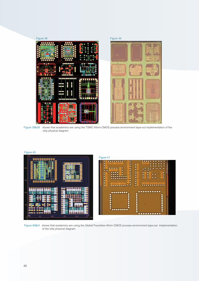
6060
Figure 40&41 shows that academics are using the Global Foundries 40nm CMOS process environment tape-out implementation of the chip physical diagram
Figure 38&39 shows that academics are using the TSMC 65nm CMOS process environment tape-out implementation of the chip physical diagram
Figure 40
Figure 41
Figure 38 Figure 39
61
CIC ANNUAL REPORT 2010
61
Design Implementation Measurement Counseling Service (Hotline Service)
Regarding the implementation of IC and system design measurement technology in academia, CIC
provides consulting services (a Hotline Service) related to problems occurring following the establishment of
self-CIC, providing a service that school teachers and students could use to study with considerable help to
further enhance technical advisory service quality. In 1993 CIC established“design environment software-
cum-technology consulting,”a dedicated service mechanism for fi elding calls or e-mail, offering basic problem
classifi cation, and then referring questions to technical staff with relevant expertise, while the service ensures
continuous improvement. In 1996 CIC standardized its technical advice hotline service, and subsequently
continued to provide the service. The service has now obtained ISO 9001 certifi cation. During 2010 the service
fi elded 525 inquiries. (Tables 12 and 13)
Statistics of Services
2010 Statistics of Hotline Jan. Feb. Mar. Apr. May Jun. Jul. Aug. Sep. Oct. Nov. Dec. Total
Hotline 77 54 135 161 108 86 112 102 152 118 94 66 1265
885 Hotline 99 91 155 145 119 76 116 125 63 99 91 81 1260
Hotline Total 176 145 290 306 227 162 228 227 215 217 185 147 2525
DTS 77 60 133 159 118 85 103 90 129 118 91 70 1233
MTS 71 56 103 82 67 34 77 81 47 74 72 55 819
SDS 4 2 3 7 12 14 9 15 5 6 6 0 83
ESTS 4 7 19 24 13 13 8 8 12 12 3 2 125
Admin 0 1 0 0 0 0 1 0 0 0 0 0 2
TPD 3 3 0 5 2 1 6 3 5 1 3 3 35
CISD 17 16 32 29 15 15 24 30 17 6 10 17 228
Section Total 176 145 290 306 227 162 228 227 215 217 185 147 2525
Hotline Question Classifi cation
Jan. Feb. Mar. Apr. May Jun. Jul. Aug. Sep. Oct. Nov. Dec. Total
Software Operation 54 34 116 138 102 60 61 87 137 91 58 45 983
Design Flow 25 20 10 27 10 20 55 22 3 7 17 34 250
Cell Library 9 4 19 11 13 14 4 4 5 8 8 5 104
Chip Measurement 1 3 0 1 0 0 1 3 1 1 1 0 12
Circuit Design 6 5 25 10 10 6 7 11 5 30 14 7 136
Software Application 4 8 5 9 8 3 4 5 3 3 3 4 59
Software Installation 12 26 26 15 15 21 22 22 9 26 26 11 231
Software Download 5 5 8 5 6 5 5 8 8 10 8 4 77
IP Chang 6 3 10 10 8 3 12 17 5 5 2 4 85
License Related 13 18 31 40 26 23 15 21 16 14 13 12 242
Processing Case 1 1 0 0 0 0 0 0 0 0 0 0 2
Embedded Platform Related
0 0 0 0 0 0 0 0 0 0 0 0 0
Others 40 18 40 40 29 7 42 27 23 22 35 21 344
Total 176 145 290 306 227 162 228 227 215 217 185 147 2525
Table 12 Statistics of Technology Consulting (I)
Table 13 Statistics of Technology Consulting (II)

6262

63
CIC ANNUAL REPORT 2010
63
CIC ANNUAL REPORT 2010
6464
CIC digital and mixed-signal Tester have continued to be provided to teachers and students in academia
to provide a high quality and high-performance measurement environment. To serve high pin and high operating
frequency IC design, in 2010 CIC provided another update multiple Loadboard and established MorPACK module
for use in the ATE testing environment, and also conducted R & D on the COB462 of IC package, intended
mainly for signal pin numbers of 320 or less, but (packages are also planned for IC with pin numbers for whole
pieces exceeding 320,) due to CIC digital and mixed-signal Tester of the highest pin number for the 320 pins,
and the achieved package design is a function of the Universal Power / Ground and Signal pins share the pin,
but digital and mixed-signal Tester Device Power Supply module with Digital Channel module differs from the
original module, so CIC is currently planning the COB462 package. Digital Channels using the machine capacity
can provide the maximum number of 320 Channels, and Power / Ground and Signal Channels are separated, so
Power / Ground pins can operate independently, which is done by the external Programmable that encapsulates
the Bare Die pin number up to over 462 of the pin number. Regarding the MorPACK module in the ATE testing
environment, CIC establishes its ATE testing environment, and the testing environment uses digital and mixed-
signal Tester analysis of numerous functions to analyze the performance and features of MorPACKIC and rapidly
implement to establish the MorPACKIC function of the action, with future cooperation being open to all from
academia. Additionally, academics have worked to make (this platform easier to use), and in 2010 the digital and
mixed-signal test error -detection platform was updated to SmsrTest_v5 version 4.2. The SmarTest_v6 version
3.4 is easier to use and more fl exible, and enables easy establishment of Test Method, Test Program and other
measurement development program. This version also includes a number of other statistical analysis functions.
CIC is expected to produce a 100 Year Plan on Test Method and Test Programs, process usage, and open
academic use.
The digital and mixed-signal automatic tester of CIC was developed in 2004 and has a lifetime of more
than five years. The Tester of the original procurement vendors,“Agilent Technologies,”was split and a
subsidiary called“Verigy Limited”was spun off. From August 2004, Agilent provided 93,000 digital and mixed-
signal Testers for use by teachers and students. Moreover, digital and mixed-signal tester measurement data was
obtained from assessing a key IC performance indicators obtained by a group of Taiwanese academics. However,
since new models have been being launched for several years, and owing to a decrease in the old auto-testing
system for resource development and software support for hardware updates, existing CIC digital and mixed-
signal tester cannot be updated or expanded. This situation affects academic IC testing services, as well as the
quality and research programs operated by CIC. As a precaution, in 2010 CIC initiated a new system of digital and
mixed-signal Tester assessment, including the planning and specifi cation of a new machine with up to 512 pins, a
Data Rate of up to 800 Mbps, 58M Vector Memory and 16 group DPS channels, Additionally, consider the future
scalablility, where after expansion the module has pin number 2048 Pins, data rate 9Gbps, 64M Vector Memory
and 64 group DPS channels (compare the specifi cations listed in Table 14)
Digital and Mixed-signal IC and System
Testing Error-detection Environment
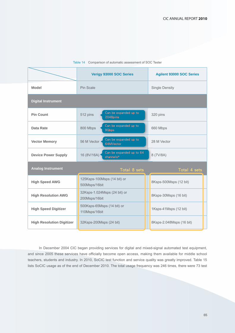
65
CIC ANNUAL REPORT 2010
65
Verigy 93000 SOC Series Agilent 93000 SOC Series
Model Pin Scale Single Density
Digital Instrument
Pin Count 512 pins 320 pins
Data Rate 800 Mbps 660 Mbps
Vector Memory 56 M Vector 28 M Vector
Device Power Supply 16 (8V/16A) 8 (7V/8A)
Analog Instrument
High Speed AWG125Ksps-100Msps (14 bit) or
500Msps/16bit8Ksps-500Msps (12 bit)
High Resolution AWG32Ksps-1.024Msps (24 bit) or
200Msps/16bit8Ksps-30Msps (16 bit)
High Speed Digitizer500Ksps-65Msps (14 bit) or
110Msps/16bit1Ksps-41Msps (12 bit)
High Resolution Digitizer 32Ksps-200Msps (24 bit) 8Ksps-2.048Msps (16 bit)
Can be expanded up to 2048pins
Can be expanded up to 9Gbps
rCan be expanded up to 64MVector
) 8Can be expanded up to 64 channels*
Total 8 sets Total 4 sets
Table 14 Comparison of automatic assessment of SOC Tester
In December 2004 CIC began providing services for digital and mixed-signal automated test equipment,
and since 2005 these services have officially become open access, making them available for middle school
teachers, students and industry. In 2010, SoCIC test function and service quality was greatly improved. Table 15
lists SoCIC usage as of the end of December 2010. The total usage frequency was 246 times, there were 73 test
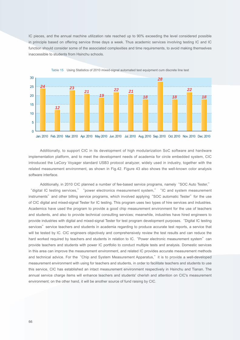
6666
IC pieces, and the annual machine utilization rate reached up to 90% exceeding the level considered possible
in principle based on offering service three days a week. Thus academic services involving testing IC and IC
function should consider some of the associated complexities and time requirements, to avoid making themselves
inaccessible to students from Hsinchu schools.
30
25
20
15
10
5
0
Jan. 2010 Feb. 2010 Mar. 2010 Apr. 2010 May 2010 Jun. 2010 Jul. 2010 Aug. 2010 Sep. 2010 Oct. 2010 Nov. 2010 Dec. 2010
24
12
2321
1922 21
18
28
18
22
18
Table 15 Using Statistics of 2010 mixed-signal automated test equipment cum discrete line test
Additionally, to support CIC in its development of high modularization SoC software and hardware
implementation platform, and to meet the development needs of academia for circle embedded system, CIC
introduced the LeCory Voyager standard USB3 protocol analyzer, widely used in industry, together with the
related measurement environment, as shown in Fig.42. Figure 43 also shows the well-known color analysis
software interface.
Additionally, in 2010 CIC planned a number of fee-based service programs, namely“SOC Auto Tester,”
“digital IC testing services,”“power electronics measurement system,”“IC and system measurement
instruments”and other billing service programs, which involved applying“SOC automatic Tester”for the use
of CIC digital and mixed-signal Tester for IC testing. This program uses two types of hire services and industries.
Academics have used the program to provide a good chip measurement environment for the use of teachers
and students, and also to provide technical consulting services; meanwhile, industries have hired engineers to
provide industries with digital and mixed-signal Tester for test program development purposes.“Digital IC testing
services”service teachers and students in academia regarding to produce accurate test reports, a service that
will be tested by IC. CIC engineers objectively and comprehensively review the test results and can reduce the
hard worked required by teachers and students in relation to IC.“Power electronic measurement system”can
provide teachers and students with power IC portfolio to conduct multiple tests and analysis. Domestic services
in this area can improve the measurement environment, and related IC provides accurate measurement methods
and technical advice. For the“Chip and System Measurement Apparatus,”it is to provide a well-developed
measurement environment with using for teachers and students, in order to facilitate teachers and students to use
this service, CIC has established an intact measurement environment respectively in Hsinchu and Tianan. The
annual service charge items will enhance teachers and students' cherish and attention on CIC's measurement
environment; on the other hand, it will be another source of fund raising by CIC.
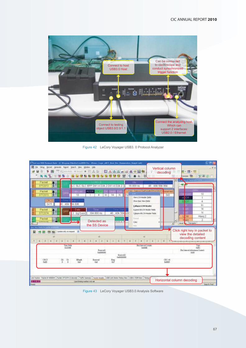
67
CIC ANNUAL REPORT 2010
67
Connect to testingobject USB3.0/2.0/1.1
Connect to hostUSB3.0 Host
Can be connected to oscilloscope and
conduct synochronized trigger function
Connect the analyzing host,Which can
support 2 interfaces:USB2.0 / Ethernet
Figure 42 LeCory Voyager USB3. 0 Protocol Analyzer
Detected as the SS Device
Click right key in packet to view the detailed decoding content
Vertical columndecoding
Horizontal column decoding
Figure 43 LeCory Voyager USB3.0 Analysis Software
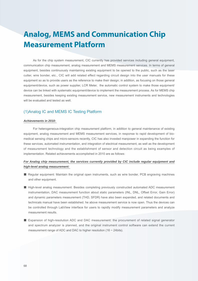
6868
As for the chip system measurement, CIC currently has provided services including general equipment,
communication chip measurement, analog measurement and MEMS measurement services. In terms of general
equipment, besides continuously maintaining existing equipment to be opened to the public, such as the laser
cutter, wire bonder, etc., CIC will add related effect regarding circuit design into the user manuals for these
equipment so as to provide users as the reference to make their design; in addition, as focusing on those general
equipment/device, such as power supplier, LCR Meter, the automatic control system to make those equipment/
device can be linked with systematic equipment/device to implement the measurement process. As for MEMS chip
measurement, besides keeping existing measurement service, new measurement instruments and technologies
will be evaluated and tested as well.
(1)Analog IC and MEMS IC Testing Platform
Achievements in 2010:
For heterogeneous-integration chip measurement platform, in addition to general maintenance of existing
equipment, analog measurement and MEMS measurement services, in response to rapid development of bio-
medical sensing chips and micro-sensors recently, CIC has also invested manpower in expanding the function for
these services, automated instrumentation, and integration of electrical measurement, as well as the development
of measurement technology and the establishment of sensor and detection circuit as being examples of
implementation. Related achievements accomplished in 2010 are as follows:
For Analog chip measurement, the services currently provided by CIC include regular equipment and
high-level analog measurement:
■ Regular equipment: Maintain the original open instruments, such as wire bonder, PCB engraving machines
and other equipment.
■ High-level analog measurement: Besides completing previously constructed automated ADC measurement
instrumentation, DAC measurement function about static parameters (INL, DNL, Offset Error, Gain Error)
and dynamic parameters measurement (THD, SFDR) have also been expanded, and related documents and
technicals manual have been established. he above measurement service is now open. Thus the devices can
be controlled through LabView interface for users to rapidly modify measurement parameters and analyze
measurement results.
■ Expansion of high-resolution ADC and DAC measurement: the procurement of related signal generator
and spectrum analyzer is planned, and the original instrument control software can extend the current
measurement range of ADC and DAC to higher resolution (16 ~ 24bits).
Analog, MEMS and Communication Chip
Measurement Platform
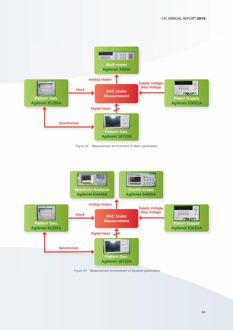
69
CIC ANNUAL REPORT 2010
69
Multi-meterAgilenet 3458A
Pattern Gen.Agilenet 16720A
Power SupplyAgilenet E3631A
DAC UnderMeasurement
Pattern Gen.Agilenet 81250A
Analog Output
Clock
Supply Voltage,Bias Voltage
Digital Input
Synchronize
Figure 44 Measurement environment of static parameters
Pattern Gen.Agilenet 16720A
Power SupplyAgilenet E3631A
DAC UnderMeasurement
Pattern Gen.Agilenet 81250A
Oscillo scopeAgilenet 54855A
Analog Output
Clock
Supply Voltage,Bias Voltage
Digital Input
Synchronize
Spectrum AnalyzerAgilenet E4440A
Figure 45 Measurement environment of dynamic parameters
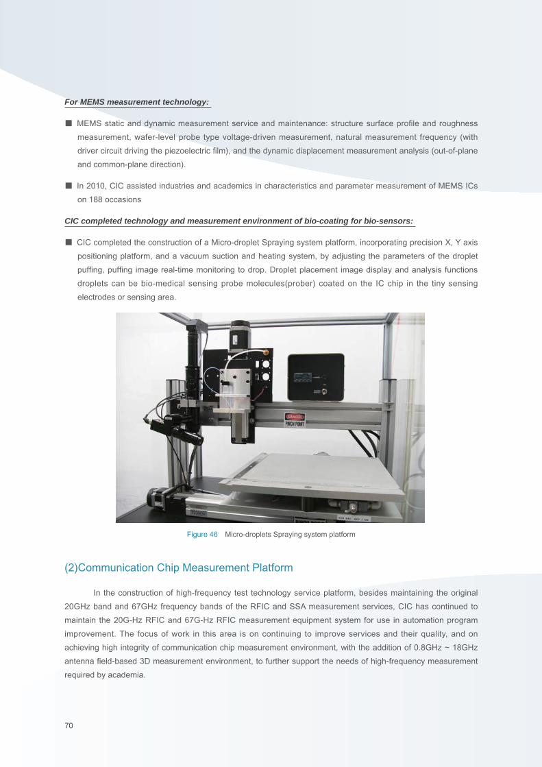
7070
For MEMS measurement technology:
■ MEMS static and dynamic measurement service and maintenance: structure surface profi le and roughness
measurement, wafer-level probe type voltage-driven measurement, natural measurement frequency (with
driver circuit driving the piezoelectric fi lm), and the dynamic displacement measurement analysis (out-of-plane
and common-plane direction).
■ In 2010, CIC assisted industries and academics in characteristics and parameter measurement of MEMS ICs
on 188 occasions
CIC completed technology and measurement environment of bio-coating for bio-sensors:
■ CIC completed the construction of a Micro-droplet Spraying system platform, incorporating precision X, Y axis
positioning platform, and a vacuum suction and heating system, by adjusting the parameters of the droplet
puffi ng, puffi ng image real-time monitoring to drop. Droplet placement image display and analysis functions
droplets can be bio-medical sensing probe molecules(prober) coated on the IC chip in the tiny sensing
electrodes or sensing area.
Figure 46 Micro-droplets Spraying system platform
(2)Communication Chip Measurement Platform
In the construction of high-frequency test technology service platform, besides maintaining the original
20GHz band and 67GHz frequency bands of the RFIC and SSA measurement services, CIC has continued to
maintain the 20G-Hz RFIC and 67G-Hz RFIC measurement equipment system for use in automation program
improvement. The focus of work in this area is on continuing to improve services and their quality, and on
achieving high integrity of communication chip measurement environment, with the addition of 0.8GHz ~ 18GHz
antenna fi eld-based 3D measurement environment, to further support the needs of high-frequency measurement
required by academia.
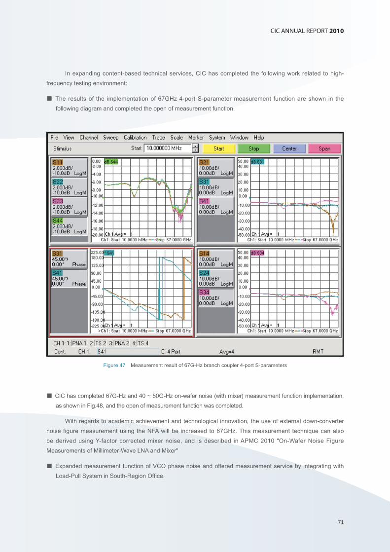
71
CIC ANNUAL REPORT 2010
71
In expanding content-based technical services, CIC has completed the following work related to high-
frequency testing environment:
■ The results of the implementation of 67GHz 4-port S-parameter measurement function are shown in the
following diagram and completed the open of measurement function.
Figure 47 Measurement result of 67G-Hz branch coupler 4-port S-parameters
■ CIC has completed 67G-Hz and 40 ~ 50G-Hz on-wafer noise (with mixer) measurement function implementation,
as shown in Fig.48, and the open of measurement function was completed.
With regards to academic achievement and technological innovation, the use of external down-converter
noise figure measurement using the NFA will be increased to 67GHz. This measurement technique can also
be derived using Y-factor corrected mixer noise, and is described in APMC 2010 "On-Wafer Noise Figure
Measurements of Millimeter-Wave LNA and Mixer"
■ Expanded measurement function of VCO phase noise and offered measurement service by integrating with
Load-Pull System in South-Region Offi ce.
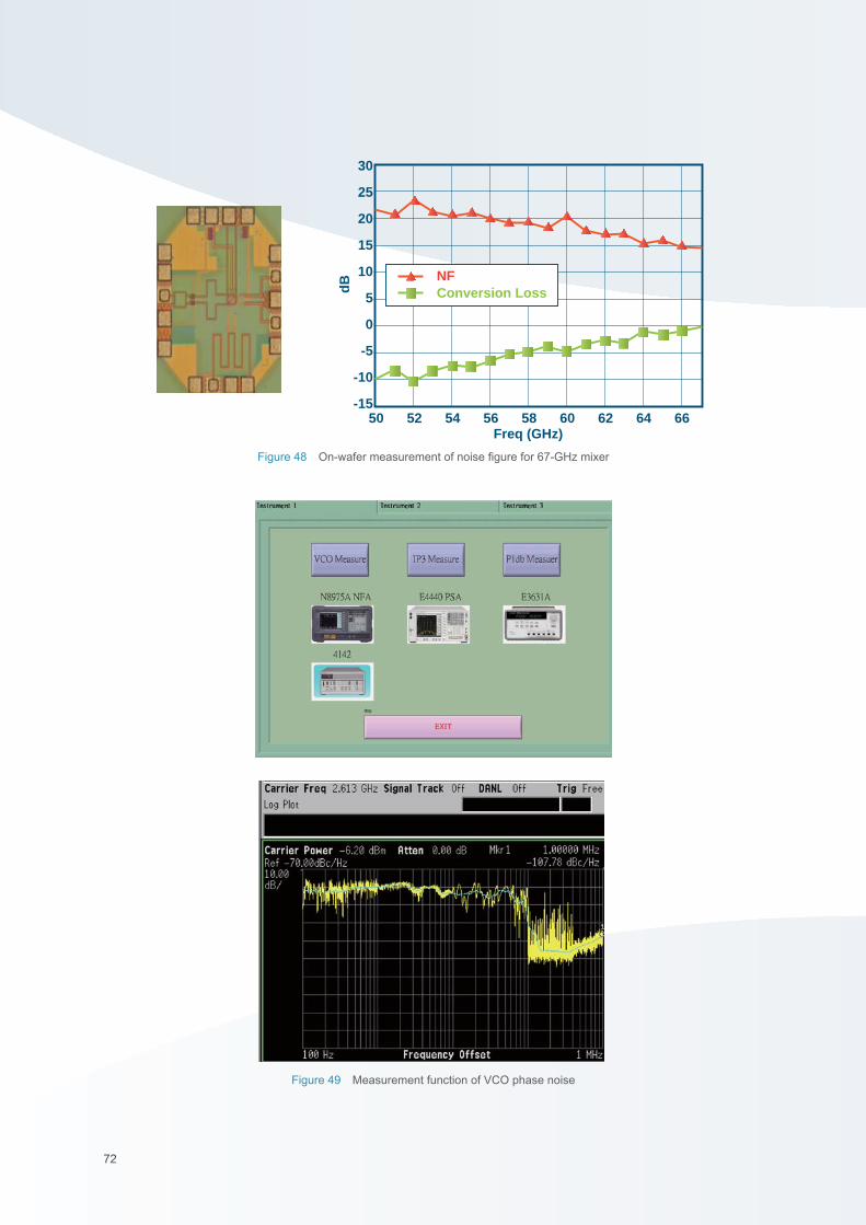
7272
30
25
20
15
10
5
0
-5
-10
-1550 52 54 56 58 60 62 64 66
Freq (GHz)
dB NF
Conversion Loss
Figure 48 On-wafer measurement of noise fi gure for 67-GHz mixer
Figure 49 Measurement function of VCO phase noise
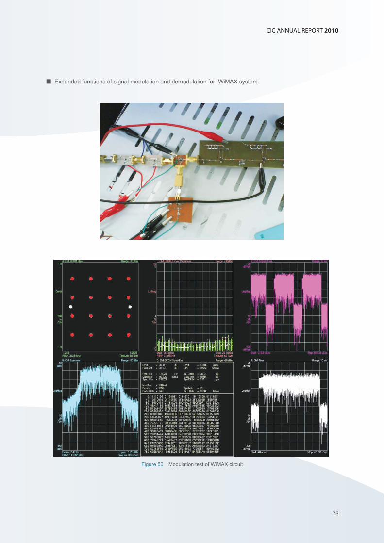
73
CIC ANNUAL REPORT 2010
73
Figure 50 Modulation test of WiMAX circuit
■ Expanded functions of signal modulation and demodulation for WiMAX system.
7474
■ Completed construction of 0.8GHz ~ 18GHz antenna fi eld-based 3D measurement environment and offered
the service for measurement of parameters including VSWR, Directivity, Gain, Beam-width, Side-lobe Levels,
Cross Polar Discrimination, 3D radiation pattern, etc.
(a)
(b)
75
CIC ANNUAL REPORT 2010
75
Figure 51 0.8GHz ~ 18GHz antenna-based 3D measurement environment
(c)

7676

77
CIC ANNUAL REPORT 2010
77
CIC ANNUAL REPORT 2010
7878
CIC, has established IC design training courses and e-Learning courses to cultivate SoC design talents,
and has also held IC design and software design contests to encourage college and university students to engage
in IC Design. Moreover, CIC has incubated practical design ability to increase student learning interest and
improve Taiwan's IC Design level and realize the vision of the MOE of“VLSI and system Design.”Furthermore,
to effectively distribute information, CIC has regularly issued e-Papers, and is coordinating with NARL to promote
the public education activities. One goal of this public education has been to help the outside world understand
the business and function of CIC so as to encourage more students to participate in research on SoC design. The
following sections demonstrate the achievements of CIC in relation to incubating SoC design talent during 2010.
7166
No.of students
9000
8000
7000
6000
5000
4000
3000
2000
1000
090 91 92 93 94 95 96 97 98 99
8227 80977667
4012
6835
8419 8423
7369
6046
Figure 52 Course Types, Frequency and Participants Over the Years
36
47 47 46
37
45 4444 44 44171
163 168166
146162
183164
140
175
50
45
40
35
30
25
20
15
10
5
0
200
180
160
140
120
100
80
60
40
20
090 91 92 93 94 95 96 97 98 99
Course Type No.of classes
Education Programs
To incubate SoC design talent, CIC has opened related training courses focused on different design
methods, including Full-Custom IC Design, Cell-Based IC Design, MEMS, Embedded system, FPGA Design, IC
Testing, RF/MMIC Design and SoC/IP, etc. In recent years, since SoC/IP design, high-frequency circuit design
and systematic design have become increasingly important, training courses are being expanded by adding more
content focused on these fi elds. Generally speaking, in 2010, CIC offered 175 sessions as part of 44 training
courses in seven categories, most of which were served by CIC engineers. Approximately 6,046 individuals,
including school teachers and students, have participated in these training courses (as shown in Fig.52).
Additionally, many participants have applied the e-learning courses in this year.
79
CIC ANNUAL REPORT 2010
79
E-learning Courses
To expand the base of IC designers, CIC also provided the unlimited e-Learning method to achieve the
goals associated with the 3E strategy: Economical, Effective and Effi cient. In 2010, CIC provided a total of ten
e-Learning courses (as shown in the following table), provided to 3,048 e-learning students.
Item e-Learning Course Title
Course 1 HSPICE
Course 2 Full-Custom IC Design Concept
Course 3 VHDL
Course 4 RF CMOS IC Design
Course 5 From Plan to Closure, what is Verifi cation Process Automation
Course 6 Introduction of Mixed-Signal Design Environment, Demo based on PLL Design
Course 7 Understand how to use Novas' Verdi Debug system
Course 8 Laker
Course 9 MMIC Design
Course 10 ADS-Circuit
8080
Contest
2010 IC Design Contest
For years the Education Improvement Program has attempted to encourage students to study IC at tertiary
level, develop practical design capabilities to stimulate their interest in learning, and enhance the implementation
of ROC IC design standards and the Ministry of Education's "VLSI circuit and system design". “2010 University
IC Design Contest“ hosted by the Advisory Offi ce of the Ministry of Education, SoC Consortium, National Yunlin
University of Science & Technology and CIC, this contest is sub-divided into 6 groups as follows: university group
of full-custom design, involving a total of 139 teams; graduate school group of full-custom design, involving a total
of 71 teams; Analog Circuit Design, involving a total of 205 teams; university group of FPGA design, involving
a total of 174 teams; university group of the standard component digital circuit design (Cell Based Design, 20
teams in total), and graduate school group of the standard component digital circuit design (Cell Based Design,
193 teams in total). A total of 732 teams were involved, representing 1,454 participants, and the fi nals involved
223 teams.
CIC designed questions for the contest categories, for the standard components and digital circuit design
group, those competitors only need to complete a logic Gate Level Design in the preliminary round; in addition,
they have to complete a Physical Design in the fi nals then. Competitors in the Full-custom Design group need
to complete the circuit and its related layout within limited time by using the full-custom design to meet the
specifications of the circuit and the implemented layout design. Programmable Logic Design only needed to
complete the logic circuit design and functional implementation (Functional Simulation) in the preliminaries; in the
fi nals, they need to complete the FPGA design (including Logic Design, FPGA Synthesis, Pin Assignment, FPGA
P & R, Confi guration File Generation and download of circuit to the system development board for implementation)
that meet standards. Competitors of the analog circuit design group need to apply the technology reports that
provided by designated units within the limited available time to complete the chip design to meet the standards
(including pre-simulation, layout, DRC, LVS and post-simulation). The topic of this contest is very interesting with
high applicability which combined with the hot topic of iPhone nowadays, and allowed students to experience the
life of IC design applications so as to inspire them to develop better applications and software in the future.
2010 Code-O-Rama Design Contest
In the embedded software design contest conducted since 1995, CIC has begun to organize the Code-
O-Rama design competition. Over the years this student design competition has seen an enormous amount
of creative and practical work. In this year's competition, a total of 106 groups from elite tertiary institutions all
over Taiwan registered for a competition dealing with the theme "Smart Idea. Smarter Life". It is hoped that
this competition can stimulate students to imagine the future of intelligent life. Compared to students not only
the current entry extract from the daily needs of creative and design using the ARM architecture, and open up
the future to understand the possibilities related to intelligent life, including those possibilities that are creative,
technical, convenient, and have signifi cantly improved integrity.
81
CIC ANNUAL REPORT 2010
81
2010 University IC Computer-Aid Design (CAD) Contest
The contest is designed to encourage college students to engage in R&D on IC Computer-Aid Design
(CAD) tools, develop actual design capacity and enhance student interest in learning, thus cultivating experienced
personnel able to improve ROC IC CAD standards. The contest was organized by the Ministry of Education, and
hosted by the National Institute of Electronic Engineering, National Taiwan University. The competition was held
on May 28, on the ninth fl oor of the Hsinchu nanoelectronics research center. Participants competing in different
categories were divided into groups and questions were distributed to them. Two kinds of entry mode existed.
The SDI Group Commission released a proposition related to the subject, and participating teams then selected
a topic and were divided into two groups based on the subject appraisal. Based on the proposition, the Marathon
Group in reference to the theses of the game, and appraised the performance of the software teams. Eligibility
was limited to students studying IC Computer-Aid Design (CAD) software fabrication at university, and teams
entered the competition under the guidance of their teachers. Only full time students were permitted to enter
the competition.
The source of this title by six companies (Cadence, CIC, SpringSoft, Faraday, ITRI and Synopsys) is
responsible for the requirements for the program to run on a Linux operating system, compiler gcc, g + +-based,
all questions other special requirements, and the percentage of total score and mining projects. Each group
completed work on the theme at 17:00 on April 26 before uploading a written report, the program (including
executable fi les), test data and results, as well as other details, to the contest website which then published a
related announcement. In the contest held on June 5, the Marathon Group competed to implement performance
appraisal software for EDA software fabrication. The Marathon Group comprised 28 teams that participated in
the semi-fi nals and achieved a strong performance. In the Institute of Electronic Engineering, National Taiwan
University Professor Huang Junlang and co-host Professor Huang Zhongyang co-operated with CIC. The entire
CAD contest oral report of the site will continue to encourage promising domestic students to pursue infinite
creative thinking and R & D design capability, nurturing the next generation of Taiwan IC Computer-Aid Design
(CAD) professionals, who should shine on the international stage.
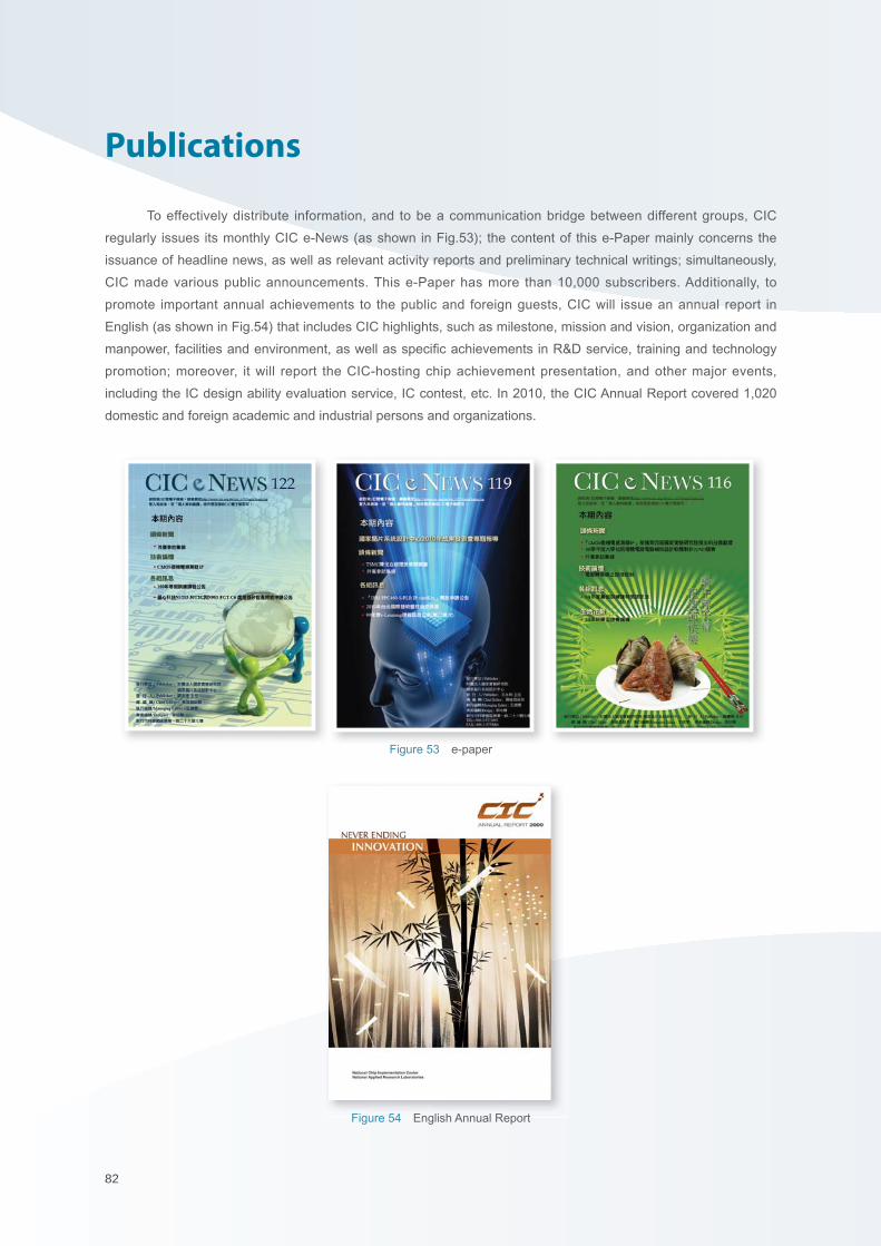
8282
Publications
To effectively distribute information, and to be a communication bridge between different groups, CIC
regularly issues its monthly CIC e-News (as shown in Fig.53); the content of this e-Paper mainly concerns the
issuance of headline news, as well as relevant activity reports and preliminary technical writings; simultaneously,
CIC made various public announcements. This e-Paper has more than 10,000 subscribers. Additionally, to
promote important annual achievements to the public and foreign guests, CIC will issue an annual report in
English (as shown in Fig.54) that includes CIC highlights, such as milestone, mission and vision, organization and
manpower, facilities and environment, as well as specifi c achievements in R&D service, training and technology
promotion; moreover, it will report the CIC-hosting chip achievement presentation, and other major events,
including the IC design ability evaluation service, IC contest, etc. In 2010, the CIC Annual Report covered 1,020
domestic and foreign academic and industrial persons and organizations.
Figure 53 e-paper
Figure 54 English Annual Report
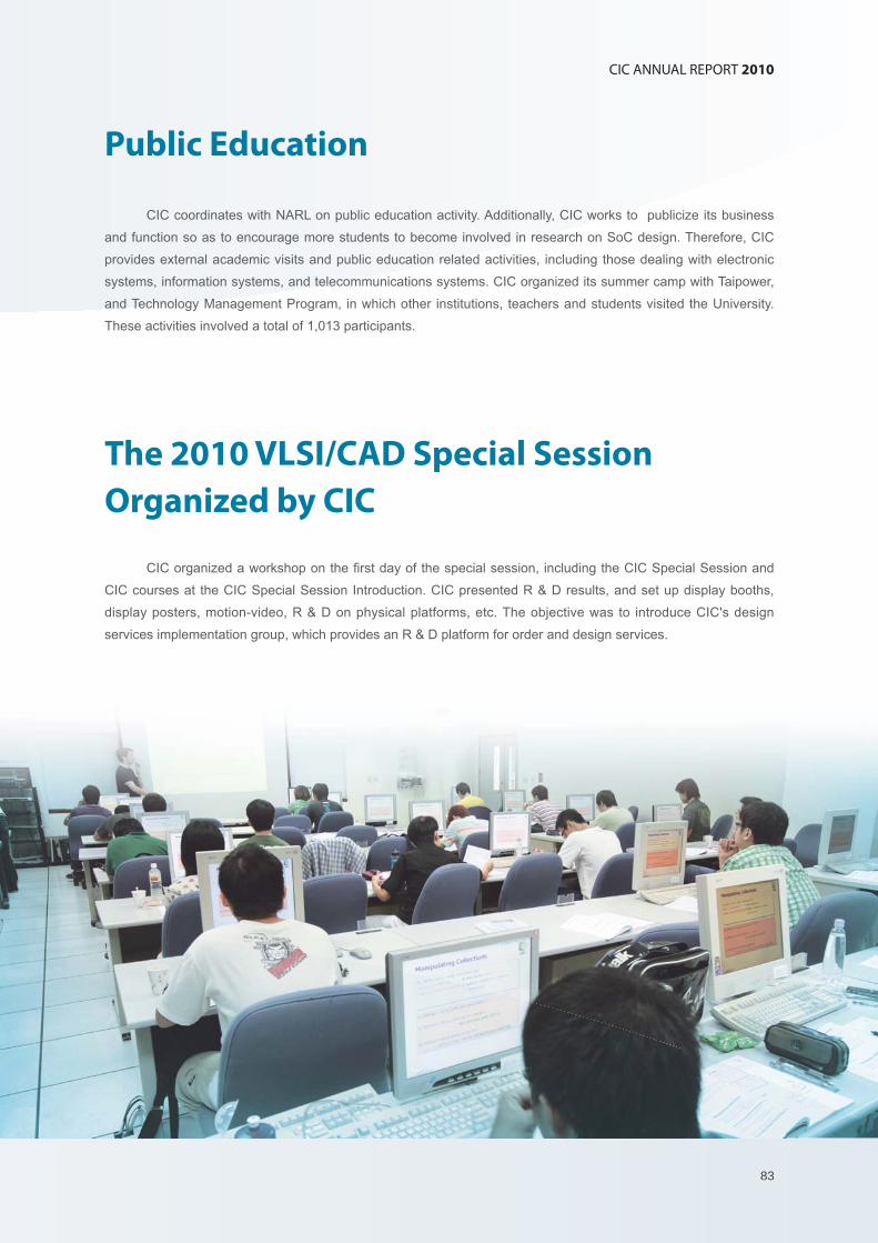
83
CIC ANNUAL REPORT 2010
83
Public Education
CIC coordinates with NARL on public education activity. Additionally, CIC works to publicize its business
and function so as to encourage more students to become involved in research on SoC design. Therefore, CIC
provides external academic visits and public education related activities, including those dealing with electronic
systems, information systems, and telecommunications systems. CIC organized its summer camp with Taipower,
and Technology Management Program, in which other institutions, teachers and students visited the University.
These activities involved a total of 1,013 participants.
The 2010 VLSI/CAD Special Session
Organized by CIC
CIC organized a workshop on the fi rst day of the special session, including the CIC Special Session and
CIC courses at the CIC Special Session Introduction. CIC presented R & D results, and set up display booths,
display posters, motion-video, R & D on physical platforms, etc. The objective was to introduce CIC's design
services implementation group, which provides an R & D platform for order and design services.
8484

85
CIC ANNUAL REPORT 2010
85
CIC ANNUAL REPORT 2010
8686
21 VLSI Design/CAD Symposium and 2010
CIC Achievement Presentation
Taiwanese academia sponsored the annual IC design annual event-VLSI Design / CAD Symposium,
held on August 3 to August 6 at the Crowne Plaza Hotel, Kaohsiung. DA held this Workshop on August 21st, in
response to the complexity of SoC design as well as the need to continue to enhance products and diversify IC
applications. The current General Assembly focuses on the theme "Towards Multiple Dimensions in SoC Design",
and brings together industry, government, research, and academic communities of advanced, on the "post-
SoC" future development, for lectures, seminars, short training courses, production of theses and other industry-
university exchanges, as well as other activities.
Over the years, CIC has actively held workshops, including related courses each year and booth display,
and this year the results of the CIC Workshop activities will be moved to the scene of the Workshop on the fi rst
day (August 3). The Special Programme of the Special Session organized by the CIC involves the CIC Party
and CIC short courses, as well as the presentation of the R & D results obtained by CIC, including research
on MorFPGA platform, CONCORD-II platform, CMOS heterogeneous integration of new technology to support
National Science Council embedded free software program, and plans to build a multi-core platform of related
results, and based on instructions during the second half of XXX, CIC will provide HV CMOS, IPD SiP, sensor
integration and other new service platforms. In addition to awards for quality IC designers, the CIC Party was held
in the evening after the prize drawing to promote CIC services, and involved a registered VLSI Workshop and
Figure 55 CIC Achievement Presentation
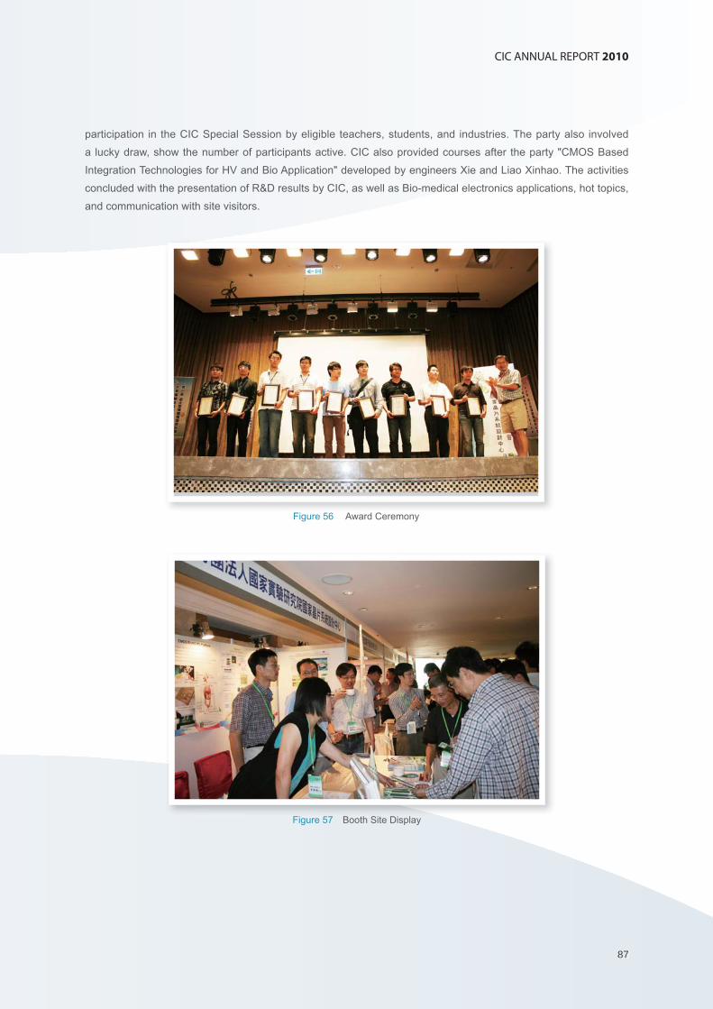
87
CIC ANNUAL REPORT 2010
87
Figure 56 Award Ceremony
Figure 57 Booth Site Display
participation in the CIC Special Session by eligible teachers, students, and industries. The party also involved
a lucky draw, show the number of participants active. CIC also provided courses after the party "CMOS Based
Integration Technologies for HV and Bio Application" developed by engineers Xie and Liao Xinhao. The activities
concluded with the presentation of R&D results by CIC, as well as Bio-medical electronics applications, hot topics,
and communication with site visitors.
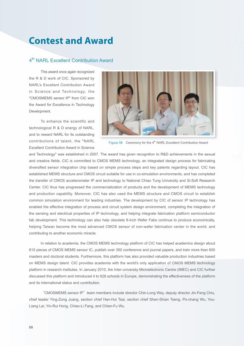
8888
Contest and Award
4th NARL Excellent Contribution Award
This award once again recognized
the R & D work of CIC. Sponsored by
NARL's Excellent Contribution Award
in Sc ience and Techno logy, the
"CMOSMEMS sensor IP" from CIC won
the Award for Excellence in Technology
Development.
To enhance the scientific and
technological R & D energy of NARL,
and to reward NARL for its outstanding
contributions of talent, the "NARL
Excellent Contribution Award in Science
and Technology" was established in 2007. The award has given recognition to R&D achievements in the sexual
and creative fi elds. CIC is committed to CMOS MEMS technology, an integrated design process for fabricating
diversified sensor integration chip based on simple process steps and key patents regarding layout. CIC has
established MEMS structure and CMOS circuit suitable for use in co-simulation environments, and has completed
the transfer of CMOS accelerometer IP and technology to National Chiao Tung University and Si-Soft Research
Center. CIC thus has progressed the commercialization of products and the development of MEMS technology
and production capability. Moreover, CIC has also used the MEMS structure and CMOS circuit to establish
common simulation environment for leading industries. The development by CIC of sensor IP technology has
enabled the effective integration of process and circuit system design environment, completing the integration of
the sensing and electrical properties of IP technology, and helping integrate fabrication platform semiconductor
fab development. This technology can also help obsolete 8-inch Wafer Fabs continue to produce economically,
helping Taiwan become the most advanced CMOS sensor of non-wafer fabrication center in the world, and
contributing to another economic miracle.
In relation to academia, the CMOS MEMS technology platform of CIC has helped academics design about
615 pieces of CMOS MEMS sensor IC, publish over 350 conference and journal papers, and train more than 600
masters and doctoral students. Furthermore, this platform has also provided valuable production industries based
on MEMS design talent. CIC provides academia with the world's only application of CMOS MEMS technology
platform in research institutes. In January 2010, the Inter-university Microelectronic Centre (IMEC) and CIC further
discussed this platform and introduced it to 628 schools in Europe, demonstrating the effectiveness of the platform
and its international status and contribution.
“CMOSMEMS sensor IP”team members include director Chin-Long Wey, deputy director Jin-Feng Chiu,
chief leader Ying-Zong Juang, section chief Han-Hui Tsai, section chief Shen-Shian Tseng, Po-chang Wu, You-
Liang Lai, Yin-Rui Hong, Chiao-Li Fang, and Chien-Fu Wu.
Figure 58 Ceremony for the 4th NARL Excellent Contribution Award
89
CIC ANNUAL REPORT 2010
89
CIC ANNUAL REPORT 2010
Invention Award in“2010 Taipei International Invention Show & Technomart”
“2010 Taipei International Invention Show & Technomart”
was held in the Taipei World Trade Center from September 30th
to October 3, 2010. Over its four day duration the event attracted
record crowds, exceeding 10 million people. In terms of scale,
the exhibition was also the largest ever, involving a total of 660
firms and 1,000 booths, displaying more diverse contents than
in previous years, and involving numerous representatives of
business, including from distributors and professional investors.
The event is currently in its sixth year. Competitions were
held at the event, and attracted 962 entries from 18 countries.
Taiwanese inventors grabbed 113 gold, 115 silver and 153 bronze
medals. Inventors from CIC achieved special honor by participating
in the"MP-SoC platform and design method" patents competition,
winning the bronze award.
The next Taipei International Invention Show & Technomart will be held in Exhibition Hall I from September
29~October 2, 2011. CIC looks forward to meeting you again in Taipei and celebrating Taiwan's 100th birthday.
Figure 59 Bronze Medal Winner and Invention in 2010 Ta ipe i In te rna t iona l Invention Show & Technomart
Figure 60 Booths in 2010 Taipei International Invention Show & Technomart
9090
TSMC Manager Ge-Li Chen Award Ceremony
CIC has rewarded TSMC Manager Ge-Li
Chen for striving to improve the academic IC design
and fabrication environment in Taiwan, and on the
morning of August 23 will present him with a Certifi cate
of Appreciation. Yeong-Her Wang, Vice President of
NARL (acting director general) relevant senior figures
from CIC will come in to thank Manager Ge-Li Chen
for actively assisting CIC in obtaining diverse advanced
processes from TSMC, promoting the domestic training
of academics, performing advanced IC design and
contributing to the boom in R&D on various electronic
and other cutting-edge technologies.
In 1987, Manager Ge-Li Chen graduated from
the Graduate Institute of Electronics, National Chiao
Tung University, and actively assisted CIC during
service TSMC made TSMC diversifi cation (CMOS Logic, MS / RF, SiGe, CIS and HV) and 90/65 nm the following
advanced process open to domestic academic circle IC design R & D use, thus promoting the fl ourishing development
of technological R&D on advanced IC design, MEMS, Bio-medical electronics and Green Energy Electrical Equipment.
The TSMC 0.13micron and 90nm processes have been announced in 2010, were synchronized with the
industry design specifications of the 65nm process and provided to CIC. CIC and TSMC cooperated to provide a
R&D platform to academia that offered the most stable and mature advanced processes, thus boosting the ability of
the Taiwanese IC industry to pursue visionary and creative chip design. The Taiwanese IC design industry displayed
significant growth in terms of numbers of published theses presented at the International Solid-State Circuits
Conference (ISSCC). This demonstrates the early and effective adoption of an academia-industry cooperation model
to cultivate high-tech talent and support high tech manufacturing with highly qualifi ed manpower.
Manager Ge-Li Chen has long actively promoted cooperation between academia and TSMC, and the company
has contributed its resources to support higher education and innovation in the area of IC design. This strong support
from TSMC has helped reduce the need for state funding of academic research in the area of IC design, as well as
reducing R&D costs in Taiwan. The support provided by Manager Ge-Li Chen to academic IC design platforms has
enabled the provision of excellent service models and effective solutions, enabling IC academic circles in Taiwan to
enjoy high-quality, advanced process technology platform research on continuous innovation, and thus keep pace
with or even gain a lead on the most promising international teams. Meanwhile, Taiwanese academics have achieved
advancements in innovation and other excellent results that can be shared with industry. This model thus is clearly
extremely helpful in terms of supporting the prosperity of the Taiwanese IC industry, and making Taiwan a major
developer of advanced technology and a trend leader.
Manager Ge-Li Chen has created a high standard of personnel training and high quality design environment at
TSMC that has contributed signifi cantly to the Taiwanese IC industry, and that has provided related research resources
to meet the R&D needs of domestic IC academic circles, as well as the various possible options such as commitment
and dedication, doing everything possible to bring to their enthusiasm and spirit was really never forget with direct praise.
Figure 61 Photo of Manager Ge-Li Chen and Deputy Director Yeong-Her Wang
Figure 61 Photo of Manager Ge Li Chen and Deputy Director
91
CIC ANNUAL REPORT 2010
91
Promulgation Ceremony for Director
General Tzi-Dar Chiueh
Following a careful selection process, Prof. Tzi-Dar Chiueh of National Taiwan University took over as
Director of CIC on November 1 in a promulgation ceremony .
The President of NARL, Wen-Hwa Chen presided over the ceremony, which was also attended by the
Deputy Minister of the National Science Council, Jing-Yang Jou; the Vice President of NARL, Yeong-Her Wang;
the Director General of Electronics and Optoelectronics Research Laboratories, ITRI, Dr. Jyuo-Min Shyu; the
Former Director General of CIC, Prof. Chin-Long Wey, and many other notable fi gures from both academia and
the research community. NARL President Wen-Hwa Chen Qi Mian expressed his wish that the new director would
display courage and commitment to reform, uphold the spirit of excellence, provide good leadership, promote
organizational and functional integration, and push the development of SoC technology for new applications.
Furthermore, NSC Deputy Minister, Jing-Yang Jou and the previous director of CIC, Prof. Chin-Long Wey
encouraged CIC to chase the excellent“tradition”and continue to promote resource sharing services, effi cient
use of resources, and enhanced production. Director General of CIC, Dr. Jyuo-Min Shyu also encouraged his
colleagues to strive to overcome IC design problems and further refine SoC and nano-process technologies
under the new director. Director General Tzi-Dar Chiueh pointed to himself as an example and encouraged his
colleagues to uphold the principles of "fairness, openness, and efficiency", the completion of cross-CIC, and
inter-field R & D program for domestic academics to provide better service and a high-tech service industry
benchmarking organization, thus enhancing the status of Taiwanese academics in international IC design
competitions, particularly in the fi eld of technical standards.
Figure 62 Promulgation Ceremony for Director General Chiueh
9292
Figure 63 NARL President Awarded the Letter of Appointment to CIC Director General Chiueh
Director General Tzi-Dar Chiueh
identif ied the main areas of research
as being high-speed digital integrated
c i rcui t , broadband communicat ions
t e c h n o l o g y a n d c o m m u n i c a t i o n s
integrated circuit system design. Director
General Chiueh, with a Ph.D. in Electrical
Engineering from the California Institute
of Technology, and soon due to return
to National Taiwan University Electrical
Engineering faculty, served as the co-
host of the National Science Council
Pro jec ts Agency NSoC convent ion
organized by the Nat ional Sc ience
Council. Furthermore, (the Ministry of
Education advanced chip system design personnel training convention on the General Union of pilot-type
projects, during 2004-2006 consultants from the SoC Technology Center helped organize a conference
for the training of advanced chip system design personnel under the auspices of the Graduate Institute
of Electronics Engineering. Currently, the Director of NTU is the professor of Department of Electrical
Engineering and Graduate Institute of Electronics Engineering. Under the leadership of Director General
Chiueh, CIC is excellently positioned to support further advances in the domestic development of integrated
circuit SoC.
The Promulgation Ceremony for the Director General of CIC was hosted by Wen-Hwa Chen
(Fig.64), President of National Applied Research Laboratories (NARL), and the Acting Director General,
Yeong-Her Wang (right) handed the official seal of CIC to the New Director General, Prof. Tzi-Dar
Chiueh (left).
Figure 63 NARL President Awarded the Letter of Appointment to CIC
Figure 64 Handing-over Ceremony for CIC Director Generals
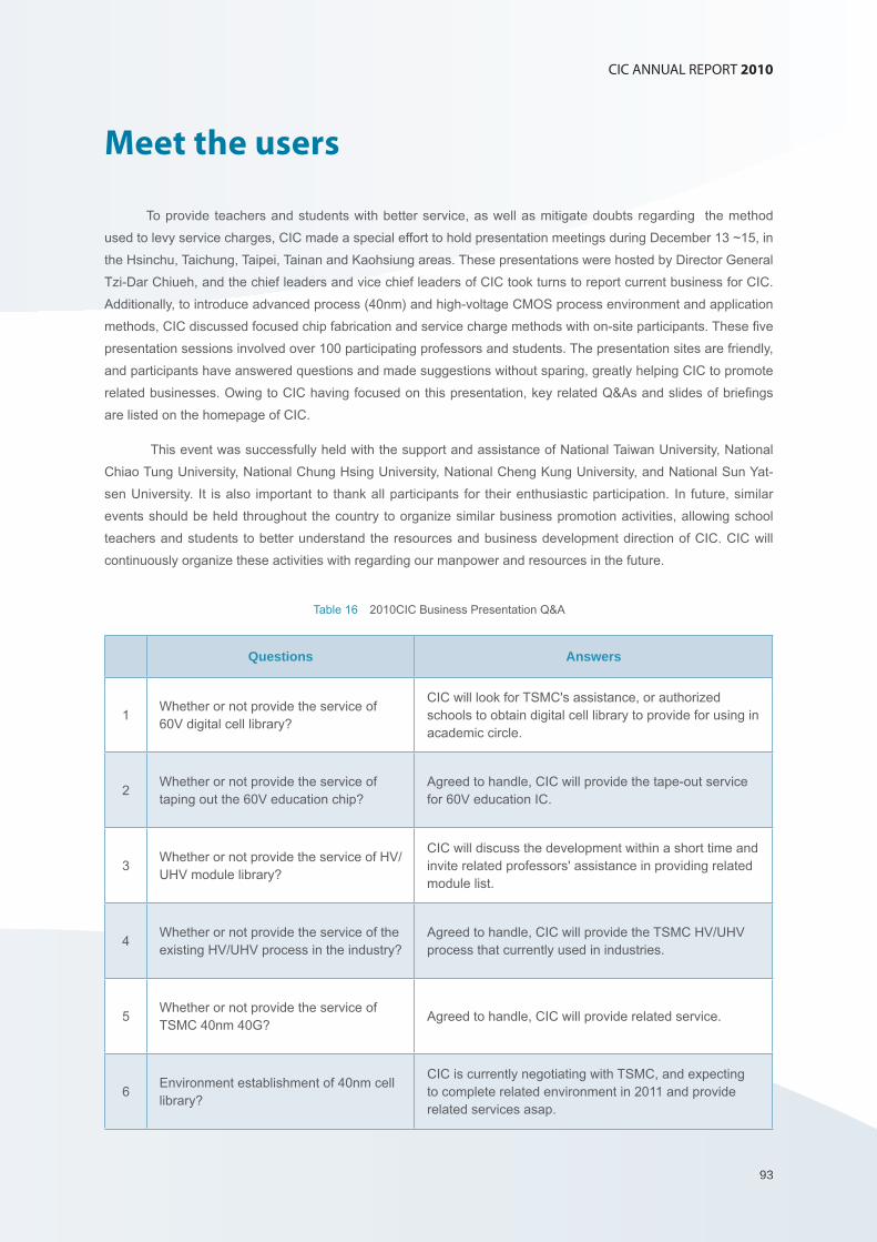
93
CIC ANNUAL REPORT 2010
93
To provide teachers and students with better service, as well as mitigate doubts regarding the method
used to levy service charges, CIC made a special effort to hold presentation meetings during December 13 ~15, in
the Hsinchu, Taichung, Taipei, Tainan and Kaohsiung areas. These presentations were hosted by Director General
Tzi-Dar Chiueh, and the chief leaders and vice chief leaders of CIC took turns to report current business for CIC.
Additionally, to introduce advanced process (40nm) and high-voltage CMOS process environment and application
methods, CIC discussed focused chip fabrication and service charge methods with on-site participants. These fi ve
presentation sessions involved over 100 participating professors and students. The presentation sites are friendly,
and participants have answered questions and made suggestions without sparing, greatly helping CIC to promote
related businesses. Owing to CIC having focused on this presentation, key related Q&As and slides of briefi ngs
are listed on the homepage of CIC.
This event was successfully held with the support and assistance of National Taiwan University, National
Chiao Tung University, National Chung Hsing University, National Cheng Kung University, and National Sun Yat-
sen University. It is also important to thank all participants for their enthusiastic participation. In future, similar
events should be held throughout the country to organize similar business promotion activities, allowing school
teachers and students to better understand the resources and business development direction of CIC. CIC will
continuously organize these activities with regarding our manpower and resources in the future.
Questions Answers
1Whether or not provide the service of 60V digital cell library?
CIC will look for TSMC's assistance, or authorized schools to obtain digital cell library to provide for using in academic circle.
2Whether or not provide the service of taping out the 60V education chip?
Agreed to handle, CIC will provide the tape-out service for 60V education IC.
3Whether or not provide the service of HV/UHV module library?
CIC will discuss the development within a short time and invite related professors' assistance in providing related module list.
4Whether or not provide the service of the existing HV/UHV process in the industry?
Agreed to handle, CIC will provide the TSMC HV/UHV process that currently used in industries.
5Whether or not provide the service of TSMC 40nm 40G?
Agreed to handle, CIC will provide related service.
6Environment establishment of 40nm cell library?
CIC is currently negotiating with TSMC, and expecting to complete related environment in 2011 and provide related services asap.
Meet the users
Table 16 2010CIC Business Presentation Q&A
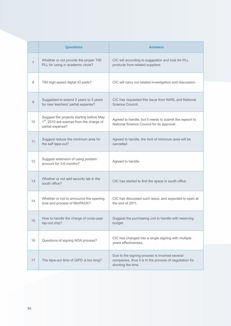
9494
Questions Answers
7Whether or not provide the proper T90 PLL for using in academic circle?
CIC will according to suggestion and look for PLL products from related suppliers
8 T90 high-speed digital IO pads? CIC will carry out related investigation and discussion.
9Suggested to extend 2 years to 3 years for new teachers' partial expense?
CIC has requested this issue from NARL and National Science Council.
10Suggest the projects starting before May 1
st, 2010 are exempt from the charge of
partial expense?
Agreed to handle, but it needs to submit the repeort to National Science Council for its approval.
11Suggest reduce the minimum area for the self tape-out?
Agreed to handle, the limit of minimum area will be cancelled
12Suggest extension of using postsim account for 3-6 months?
Agreed to handle
13Whether or not add security lab in the south offi ce?
CIC has started to fi nd the space in south offi ce.
14Whether or not to announce the opening time and process of MorPACK?
CIC has discussed such issue, and expected to open at the end of 2011.
15How to handle the charge of cross-year tap-out chip?
Suggest the purchasing unit to handle with reserving budget
16 Questions of signing NDA process?CIC has changed into a single signing with multiple years effectiveness.
17 The tape-out time of GIPD is too long?Due to the signing process is involved several companies, thus it is in the process of negotiation for shorting the time.
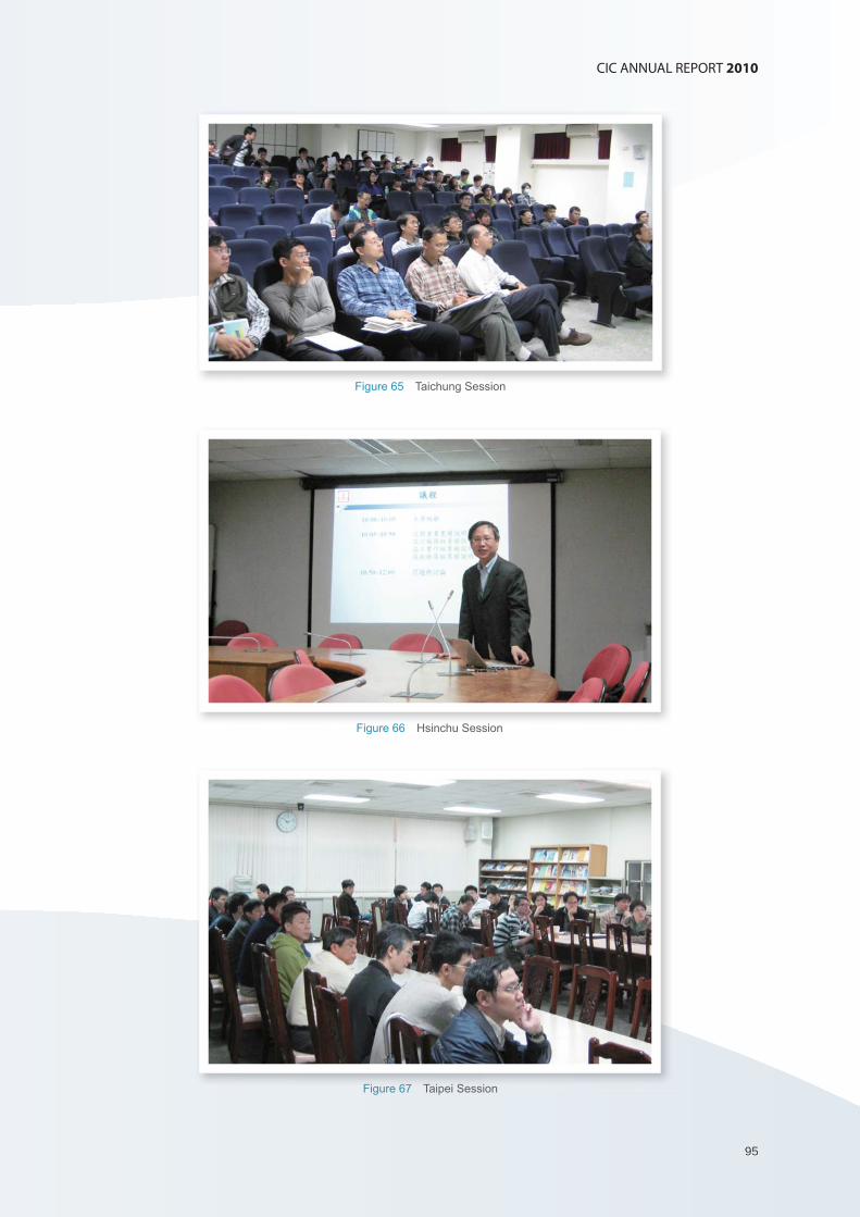
95
CIC ANNUAL REPORT 2010
95
Figure 65 Taichung Session
Figure 66 Hsinchu Session
Figure 67 Taipei Session
9696
CIC Annual Report 2010
Publisher: Chiueh, Tzi-Dar
Vice Publishers: Wang, Jiann-Jenn
Chang, Chen-Hao
Editorial Committee: Chang, Da-Chiang
Chen, Chi-Shi
Fanchiang, Yi-Chia
Huang, Chun-Ming
Juang, Ying-Zong
Wu, Chien-Ming
Wang, Jen-Chieh
Editor-in-Chief: Tsai, Wei-Chang
Editorial Team: Hsieh, Ping-Chang
Wang, Jiann-Jong
Wei-De Chien
Art Director: Lee, Chieh-Hua
Layout: CANDYSIGN Co., Ltd.
Copyright © 2011 by National Chip Implementation Center
Published by National Chip Implementation Center
National Applied Research Laboratories
7F, No. 26, Prosperity Rd. 1, Hsinchu Science Park, Taiwan, R.O.C.
TEL: 886-3-5773693
FAX: 886-3-5774064
http://www.cic.narl.org.tw
ISBN-13: 978-986-82443-5-1
Printed in Taiwan
Publishing Date: September 2011
Imprint


Recommended