ELETRÔNICA IV
Apostila de Aulas Práticas
Autor: Fernando Antônio Pinto Barúqui
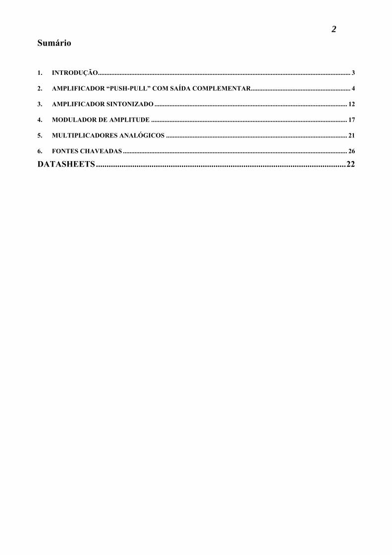
2 Sumário
1. INTRODUÇÃO........................................................................................................................................................ 3
2. AMPLIFICADOR “PUSH-PULL” COM SAÍDA COMPLEMENTAR............................................................ 4
3. AMPLIFICADOR SINTONIZADO .................................................................................................................... 12
4. MODULADOR DE AMPLITUDE ...................................................................................................................... 17
5. MULTIPLICADORES ANALÓGICOS ............................................................................................................. 21
6. FONTES CHAVEADAS ....................................................................................................................................... 26
DATASHEETS.....................................................................................................................22

3
1. Introdução O conteúdo desta apostila consiste das aulas experimentais do curso de Eletrônica IV, ministrado no Departamento de Eletrônica da Escola de Engenharia. Cada capítulo corresponde a um experimento a ser montado e estudado em laboratório. Esses experimentos foram, ao longo dos anos, sendo aprimorados didaticamente, de forma a apresentar ao aluno a constatação experimental dos conceitos básicos, e essenciais, estudados na disciplina teórica. Também são fornecidos todos os manuais dos componentes usados nos experimentos, disponibilizando ao aluno todas as informações necessárias à realização dos projetos.
4
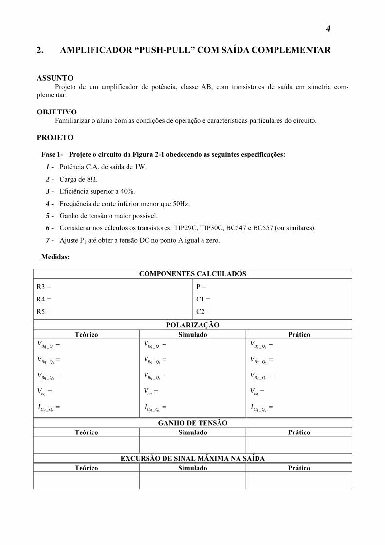
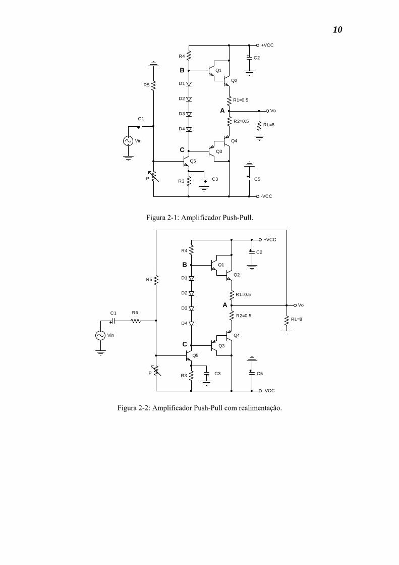
2. AMPLIFICADOR “PUSH-PULL” COM SAÍDA COMPLEMENTAR ASSUNTO Projeto de um amplificador de potência, classe AB, com transistores de saída em simetria com-plementar. OBJETIVO Familiarizar o aluno com as condições de operação e características particulares do circuito. PROJETO Fase 1- Projete o circuito da Figura 2-1 obedecendo as seguintes especificações:
1 - Potência C.A. de saída de 1W.
2 - Carga de 8Ω.
3 - Eficiência superior a 40%.
4 - Freqüência de corte inferior menor que 50Hz.
5 - Ganho de tensão o maior possível.
6 - Considerar nos cálculos os transistores: TIP29C, TIP30C, BC547 e BC557 (ou similares).
7 - Ajuste P1 até obter a tensão DC no ponto A igual a zero.
Medidas:
COMPONENTES CALCULADOS
R3 =
R4 =
R5 =
P =
C1 =
C2 =
POLARIZAÇÃO Teórico Simulado Prático
1_Bq QV =
5_Bq QV =
3_Bq QV =
oqV =
5_Cq QI =
1_Bq QV =
5_Bq QV =
3_Bq QV =
oqV =
5_Cq QI =
1_Bq QV =
5_Bq QV =
3_Bq QV =
oqV =
5_Cq QI =
GANHO DE TENSÃO Teórico Simulado Prático
EXCURSÃO DE SINAL MÁXIMA NA SAÍDA Teórico Simulado Prático
5 FREQÜÊNCIAS DE CORTE
Teórico Simulado Prático
Inferior =
Inferior =
Superior =
Inferior =
Superior =
POTÊNCIA MÁXIMA DE SAÍDA Teórico Simulado Prático
Explique a função dos seguintes componentes do circuito: R1, R2, D1, D2, D3, D4, C2 e C5
COMENTÁRIOS SOBRE OS RESULTADOS OBTIDOS
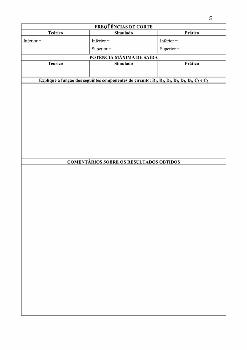
6 Curto-circuitar os pontos B e C, e esboçar a forma de onda de saída
COMENTÁRIOS SOBRE OS RESULTADOS OBTIDOS
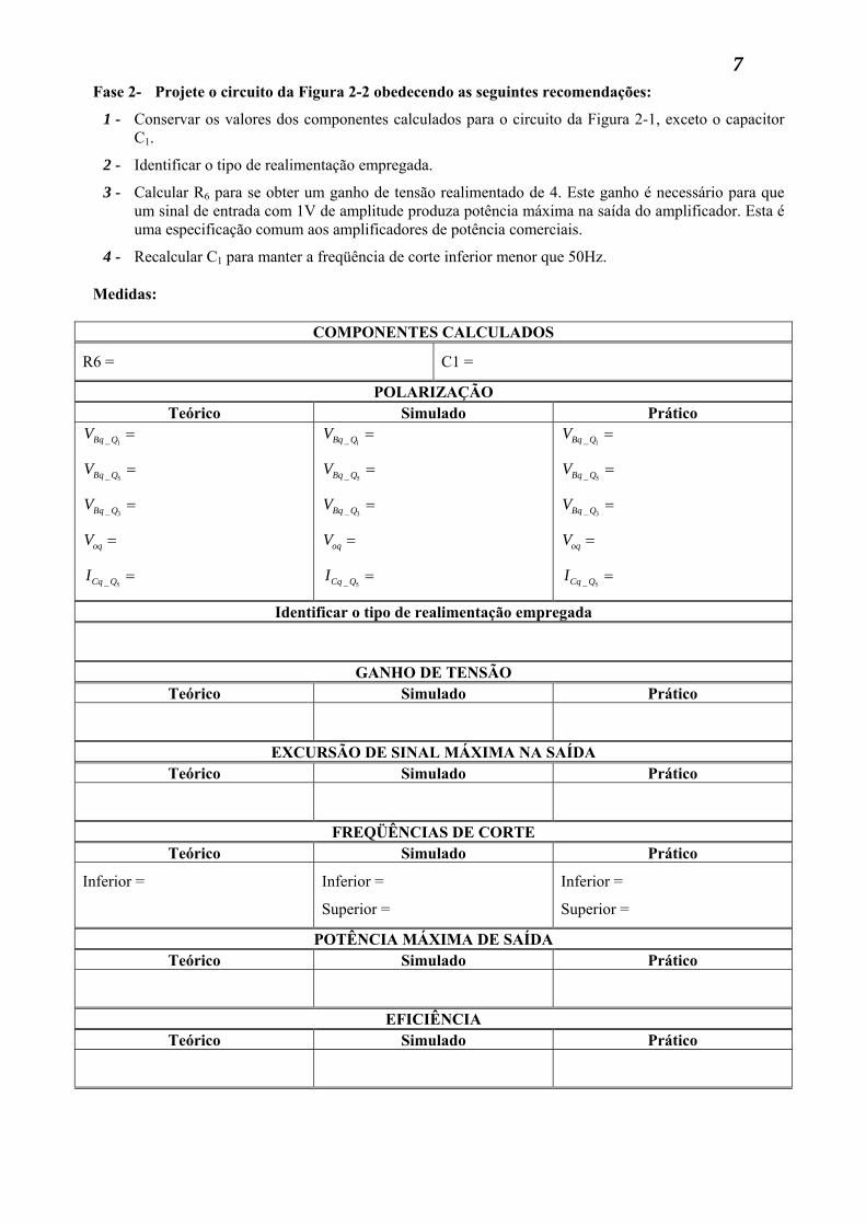
7 Fase 2- Projete o circuito da Figura 2-2 obedecendo as seguintes recomendações:
1 - Conservar os valores dos componentes calculados para o circuito da Figura 2-1, exceto o capacitor C1.
2 - Identificar o tipo de realimentação empregada.
3 - Calcular R6 para se obter um ganho de tensão realimentado de 4. Este ganho é necessário para que um sinal de entrada com 1V de amplitude produza potência máxima na saída do amplificador. Esta é uma especificação comum aos amplificadores de potência comerciais.
4 - Recalcular C1 para manter a freqüência de corte inferior menor que 50Hz.
Medidas:
COMPONENTES CALCULADOS
R6 = C1 =
POLARIZAÇÃO Teórico Simulado Prático
1_Bq QV =
5_Bq QV =
3_Bq QV =
oqV =
5_Cq QI =
1_Bq QV =
5_Bq QV =
3_Bq QV =
oqV =
5_Cq QI =
1_Bq QV =
5_Bq QV =
3_Bq QV =
oqV =
5_Cq QI =
Identificar o tipo de realimentação empregada
GANHO DE TENSÃO Teórico Simulado Prático
EXCURSÃO DE SINAL MÁXIMA NA SAÍDA Teórico Simulado Prático
FREQÜÊNCIAS DE CORTE Teórico Simulado Prático
Inferior =
Inferior =
Superior =
Inferior =
Superior =
POTÊNCIA MÁXIMA DE SAÍDA Teórico Simulado Prático
EFICIÊNCIA Teórico Simulado Prático
8 Curto-circuitar os pontos B e C, e esboçar a forma de onda de saída, comparando com a anterior
COMENTÁRIOS SOBRE OS RESULTADOS OBTIDOS
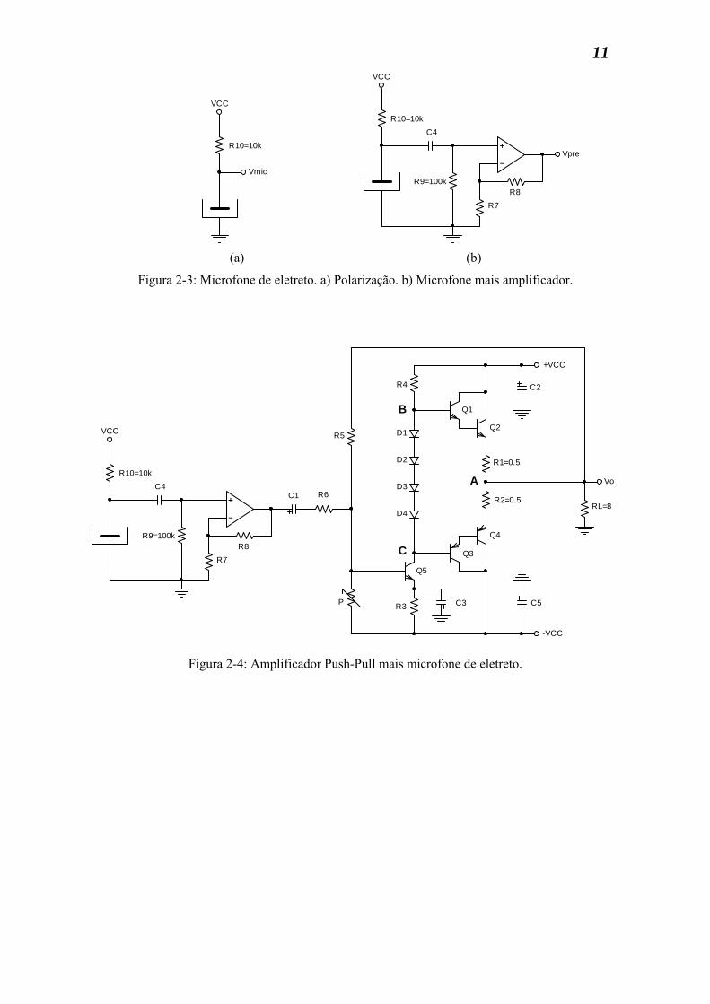
9 Fase 3- Projete o circuito da Figura 2-4 obedecendo as seguintes recomendações:
1 - Monte o circuito da Figura 2-3 (a) utilizando um microfone de eletreto e um resistor R10=10kΩ.
2 - Fale ao microfone e observe a amplitude máxima do sinal AC em Vmic.
3 - Com a tensão Vmic, projete o pré-amplificador da Figura 2-3 (b) de tal forma a se obter uma tensão máxima Vpre=1V e freqüência de corte inferior menor que 50Hz. Conecte o pré-amplificador ao amplificador da Fase 2, conforme a Figura 2-4, substitua a carga RL por um alto-falante de 8Ω e fale ao microfone.
Medidas:
COMPONENTES CALCULADOS
R7 = R8 = C4 =
GANHO DE TENSÃO DO PRÉ-AMPLIFICADOR Teórico Prático
FREQÜÊNCIAS DE CORTE DO PRÉ-AMPLIFICADOR Teórico Prático
Inferior = Inferior =
COMENTÁRIOS SOBRE OS RESULTADOS OBTIDOS
10
D1
D2
D3
D4
R4
R3
R5
RL=8
Q1
Q5
Q3
Q2
Q4Vin
R1=0.5
R2=0.5
P
+VCC
-VCC
Vo
C2
C5
C1
C3
A
C
B
Figura 2-1: Amplificador Push-Pull.
D1
D2
D3
D4
R4
R3
R5
RL=8
Q1
Q5
Q3
Q2
Q4Vin
R1=0.5
R2=0.5
P
+VCC
-VCC
Vo
C2
C5
C1
C3
C
A
B
R6
Figura 2-2: Amplificador Push-Pull com realimentação.
11
R10=10k
VCC
Vmic
+
-
C4
R8R7
R9=100k
R10=10k
Vpre
VCC
(a) (b)
Figura 2-3: Microfone de eletreto. a) Polarização. b) Microfone mais amplificador.
R6+
-
C4
R8R7
R9=100k
R10=10k
VCC D1
D2
D3
D4
R4
R3
R5
RL=8
Q1
Q5
Q3
Q2
Q4
R1=0.5
R2=0.5
P
+VCC
-VCC
Vo
C2
C5
C1
C3
C
B
A
Figura 2-4: Amplificador Push-Pull mais microfone de eletreto.
12
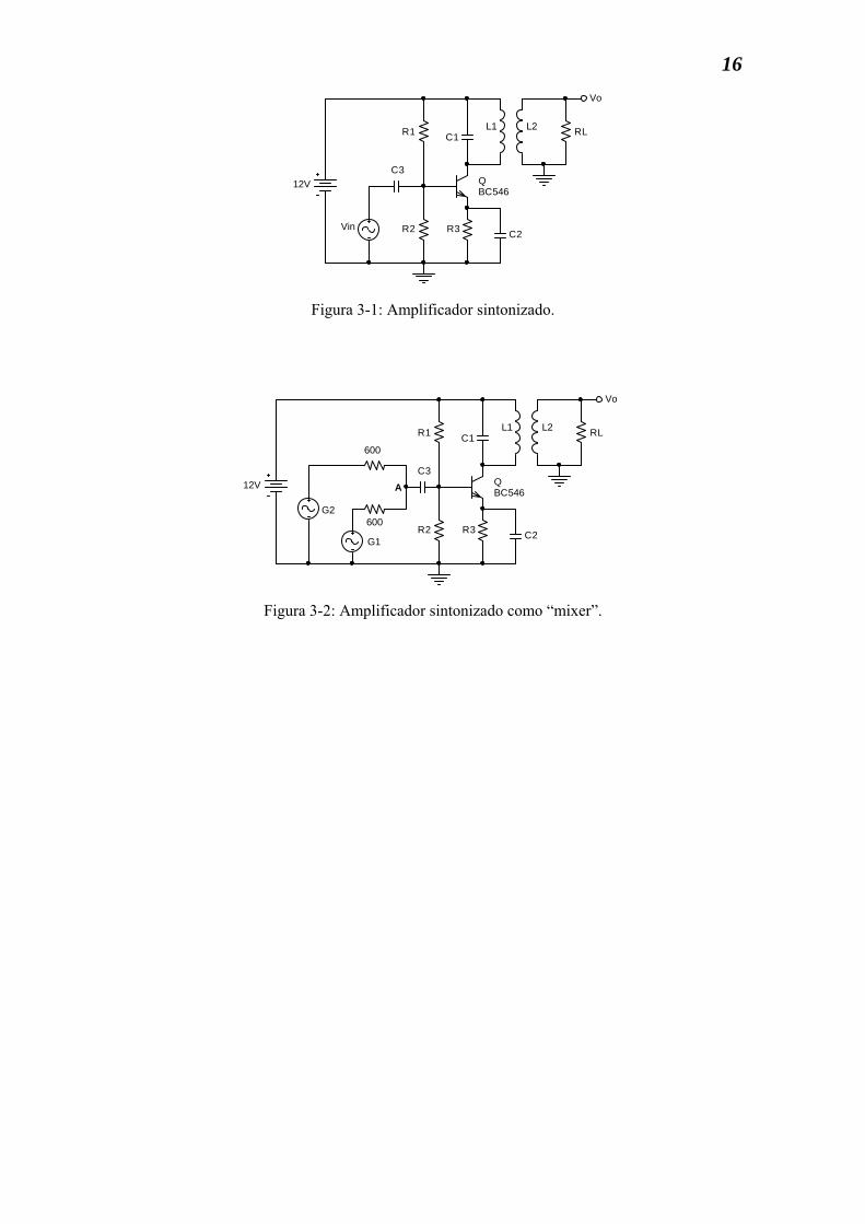
3. AMPLIFICADOR SINTONIZADO
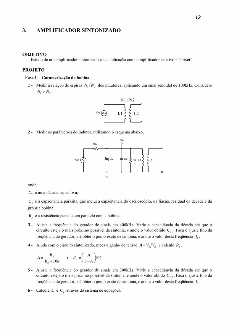
OBJETIVO Estudo de um amplificador sintonizado e sua aplicação como amplificador seletivo e “mixer”. PROJETO Fase 1- Caracterização da bobina
1 - Medir a relação de espiras 1 2N N dos indutores, aplicando um sinal senoidal de 100kHz. Considere
1 2N N> .
N1 : N2
L2L1Vin
2 - Medir os parâmetros do indutor, utilizando o esquema abaixo,
L1RpCpCv
10k
Vin
Vo
L2
onde:
VC é uma década capacitiva;
pC é a capacitância parasita, que inclui a capacitância do osciloscópio, da fiação, residual da década e da própria bobina;
pR é a resistência parasita em paralelo com a bobina.
3 - Ajuste a freqüência do gerador de sinais em 400kHz. Varie a capacitância da década até que o circuito esteja o mais próximo possível da sintonia, e anote o valor obtido 1VC . Faça o ajuste fino da freqüência do gerador, até obter o ponto exato de sintonia, e anote o valor desta freqüência 1f .
4 - Ainda com o circuito sintonizado, meça o ganho de tensão o inA V V= e calcule pR .
1010 1p
pp
R AA R kR k A
⎛ ⎞= → = ⎜ ⎟+ −⎝ ⎠
5 - Ajuste a freqüência do gerador de sinais em 300kHz. Varie a capacitância da década até que o circuito esteja o mais próximo possível da sintonia, e anote o valor obtido 2VC . Faça o ajuste fino da freqüência do gerador, até obter o ponto exato de sintonia, e anote o valor desta freqüência 2f .
6 - Calcule 1L e pC através do sistema de equações:
13
( )
( )
( )2 2
1 211 2 2 2
1 1 1 2 2 1
2 22 2 1 1
2 2 21 21 2
1
2 41
2
p V V V
V Vp
p V
f ff LL C C f f C C
C f C ff Cf fL C C
π π
π
⎧ ⎧ −=⎪ =⎪+ −⎪ ⎪→⎨ ⎨−⎪ ⎪= =⎪ ⎪ −+ ⎩⎩
7 - Calcule o fator de qualidade do indutor na freqüência 1f .
1 12p
b
RQ
f Lπ=
PARÂMETROS DO INDUTOR
L1 = Rp = Cp = Qb= N1/N2=
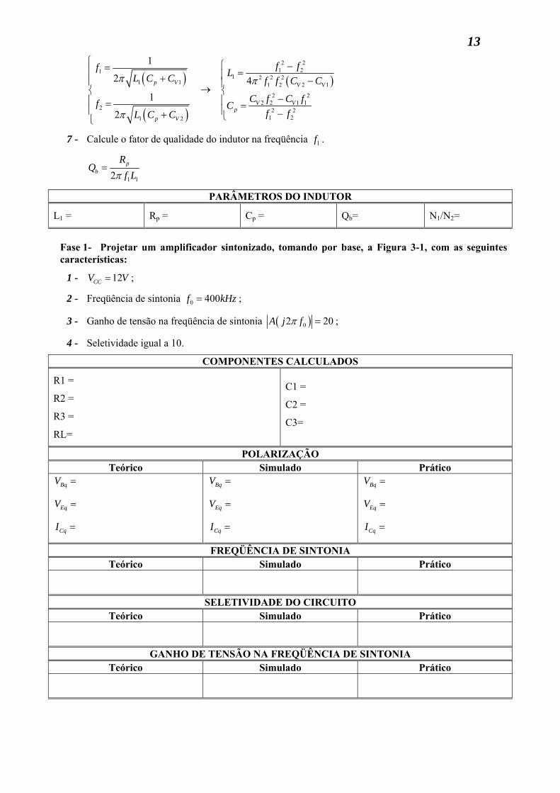
Fase 1- Projetar um amplificador sintonizado, tomando por base, a Figura 3-1, com as seguintes
características:
1 - 12CCV V= ;
2 - Freqüência de sintonia 0 400f kHz= ;
3 - Ganho de tensão na freqüência de sintonia ( )02 20A j fπ = ;
4 - Seletividade igual a 10.
COMPONENTES CALCULADOS
R1 =
R2 =
R3 =
RL=
C1 =
C2 =
C3=
POLARIZAÇÃO Teórico Simulado Prático
BqV =
EqV =
CqI =
BqV =
EqV =
CqI =
BqV =
EqV =
CqI =
FREQÜÊNCIA DE SINTONIA Teórico Simulado Prático
SELETIVIDADE DO CIRCUITO Teórico Simulado Prático
GANHO DE TENSÃO NA FREQÜÊNCIA DE SINTONIA Teórico Simulado Prático
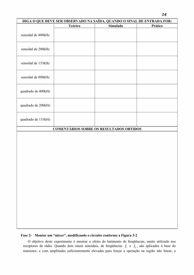
14 DIGA O QUE DEVE SER OBSERVADO NA SAÍDA, QUANDO O SINAL DE ENTRADA FOR:
Teórico Simulado Prático
senoidal de 400kHz
senoidal de 200kHz
senoidal de 133kHz
senoidal de 800kHz
quadrado de 400kHz
quadrado de 200kHz
quadrado de 133kHz
COMENTÁRIOS SOBRE OS RESULTADOS OBTIDOS
Fase 2- Montar um “mixer”, modificando o circuito conforme a Figura 3-2
O objetivo deste experimento é mostrar o efeito do batimento de freqüências, muito utilizado nos receptores de rádio. Quando dois sinais senoidais, de freqüências 1f e 2f , são aplicados à base do transistor, e com amplitudes suficientemente elevadas para forçar a operação na região não linear, a
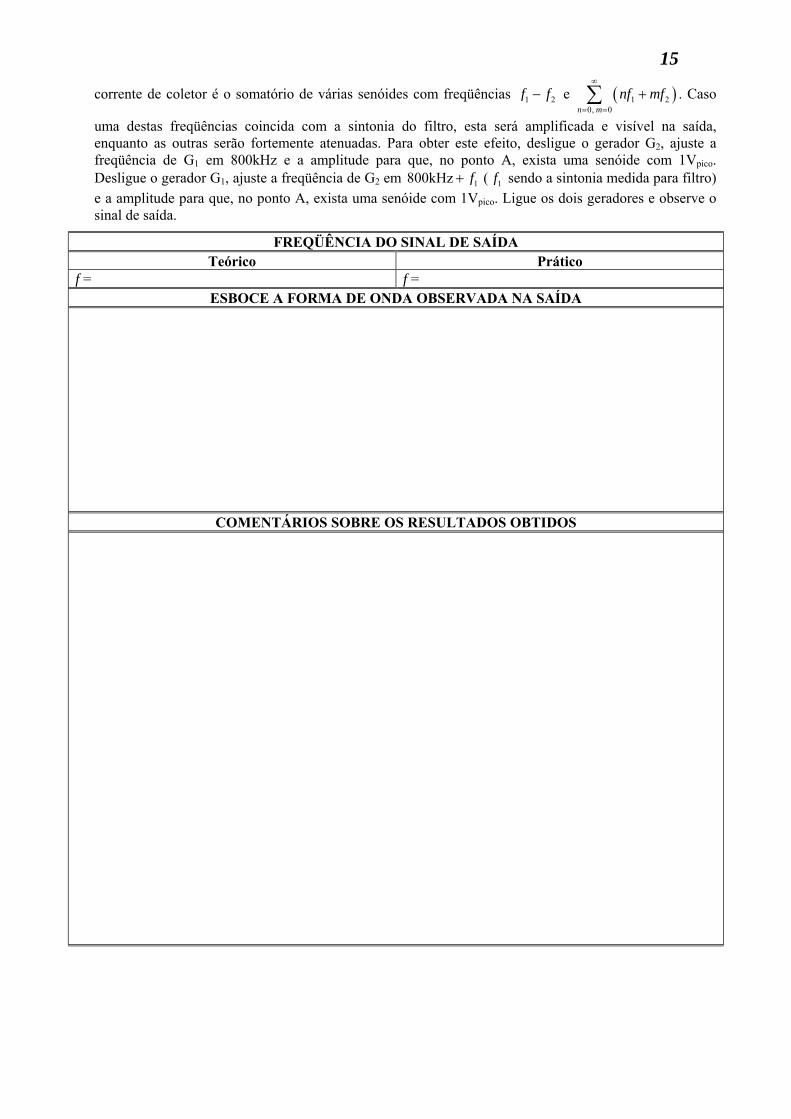
15
corrente de coletor é o somatório de várias senóides com freqüências 1 2f f− e ( )1 20, 0n m
nf mf∞
= =
+∑ . Caso
uma destas freqüências coincida com a sintonia do filtro, esta será amplificada e visível na saída, enquanto as outras serão fortemente atenuadas. Para obter este efeito, desligue o gerador G2, ajuste a freqüência de G1 em 800kHz e a amplitude para que, no ponto A, exista uma senóide com 1Vpico. Desligue o gerador G1, ajuste a freqüência de G2 em 1800kHz f+ ( 1f sendo a sintonia medida para filtro) e a amplitude para que, no ponto A, exista uma senóide com 1Vpico. Ligue os dois geradores e observe o sinal de saída.
FREQÜÊNCIA DO SINAL DE SAÍDA Teórico Prático
f = f = ESBOCE A FORMA DE ONDA OBSERVADA NA SAÍDA
COMENTÁRIOS SOBRE OS RESULTADOS OBTIDOS
16
L2L1
QBC546
C3
C2
C1 RL
R3
R1
R2
12V
Vin
Vo
Figura 3-1: Amplificador sintonizado.
L2L1
QBC546
C2
C1 RL
R3
R1
R2
12V
G1
Vo
600G2
C3
600
A
Figura 3-2: Amplificador sintonizado como “mixer”.
17
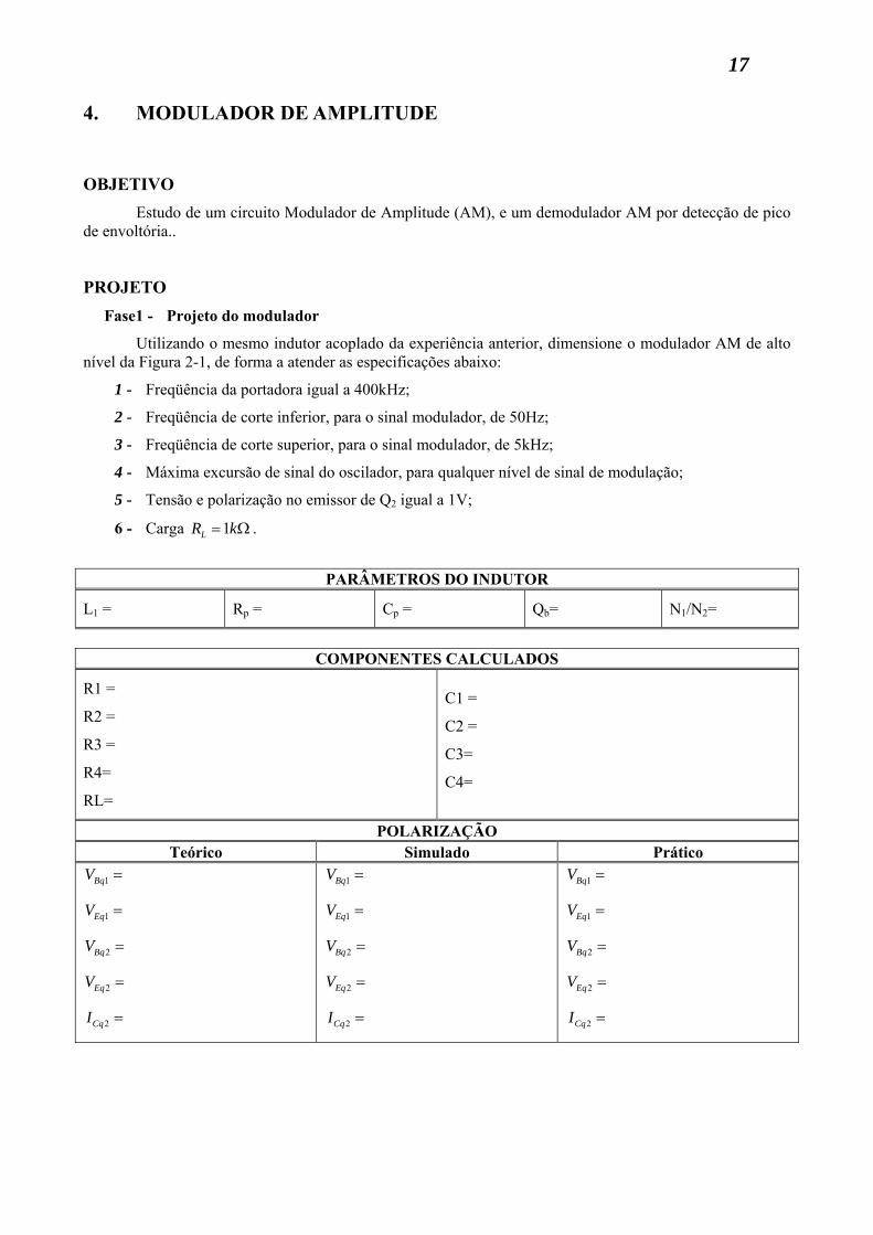
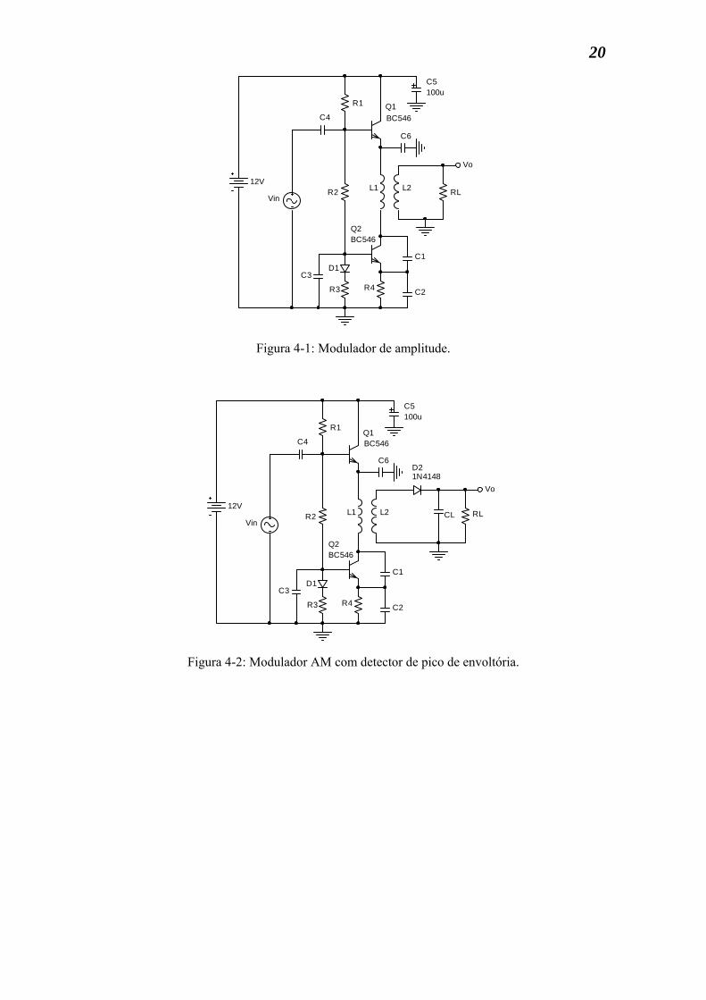
4. MODULADOR DE AMPLITUDE
OBJETIVO
Estudo de um circuito Modulador de Amplitude (AM), e um demodulador AM por detecção de pico de envoltória..
PROJETO Fase1 - Projeto do modulador
Utilizando o mesmo indutor acoplado da experiência anterior, dimensione o modulador AM de alto nível da Figura 2-1, de forma a atender as especificações abaixo:
1 - Freqüência da portadora igual a 400kHz;
2 - Freqüência de corte inferior, para o sinal modulador, de 50Hz;
3 - Freqüência de corte superior, para o sinal modulador, de 5kHz;
4 - Máxima excursão de sinal do oscilador, para qualquer nível de sinal de modulação;
5 - Tensão e polarização no emissor de Q2 igual a 1V;
6 - Carga 1LR k= Ω .
PARÂMETROS DO INDUTOR
L1 = Rp = Cp = Qb= N1/N2=
COMPONENTES CALCULADOS
R1 =
R2 =
R3 =
R4=
RL=
C1 =
C2 =
C3=
C4=
POLARIZAÇÃO Teórico Simulado Prático
1BqV =
1EqV =
2BqV =
2EqV =
2CqI =
1BqV =
1EqV =
2BqV =
2EqV =
2CqI =
1BqV =
1EqV =
2BqV =
2EqV =
2CqI =
18 FREQÜÊNCIA DE OSCILAÇÃO
Teórico Simulado Prático
Máximo Índice de Modulação sem Distorção, para um Sinal Modulador Senoidal de 50Hz Teórico Simulado Prático
Máximo Índice de Modulação sem Distorção, para um Sinal Modulador Senoidal de 500Hz Teórico Simulado Prático
Máximo Índice de Modulação sem Distorção, para um Sinal Modulador Senoidal de 5000Hz Teórico Simulado Prático
COMENTÁRIOS SOBRE OS RESULTADOS OBTIDOS
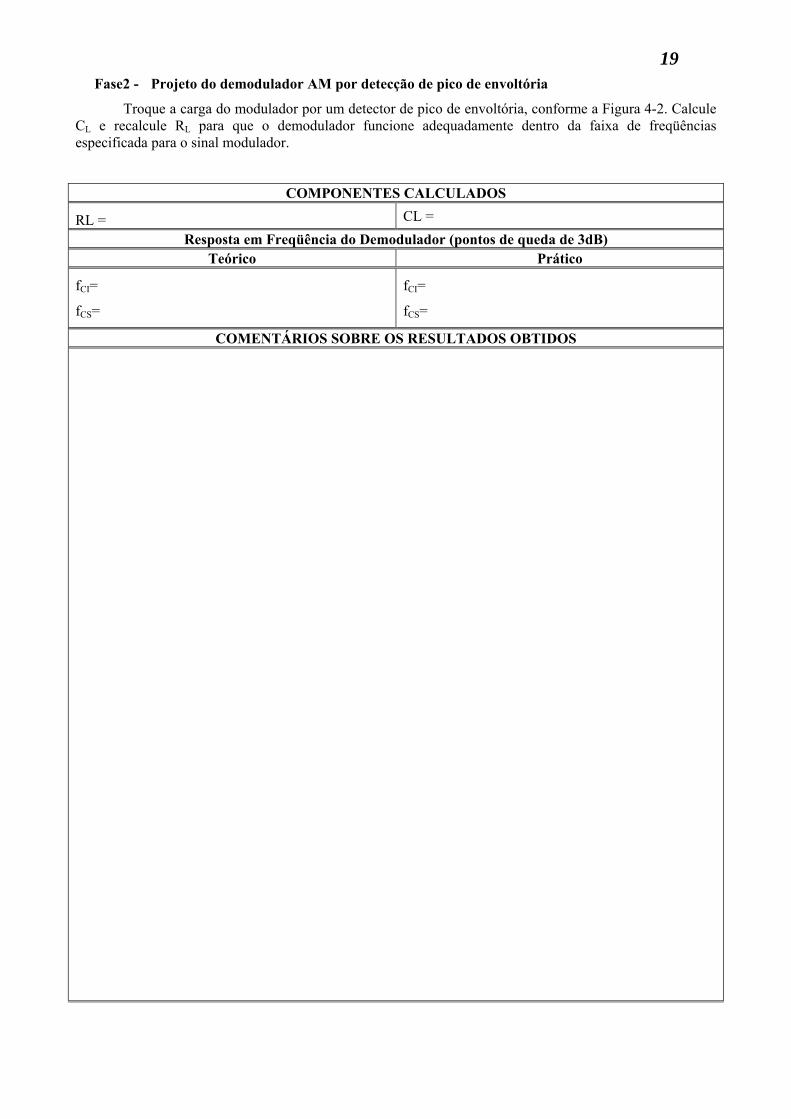
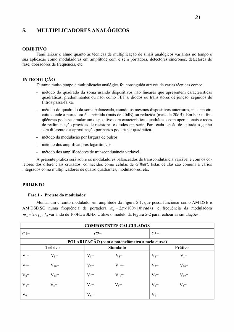
19 Fase2 - Projeto do demodulador AM por detecção de pico de envoltória
Troque a carga do modulador por um detector de pico de envoltória, conforme a Figura 4-2. Calcule CL e recalcule RL para que o demodulador funcione adequadamente dentro da faixa de freqüências especificada para o sinal modulador.
COMPONENTES CALCULADOS
RL = CL = Resposta em Freqüência do Demodulador (pontos de queda de 3dB)
Teórico Prático
fCI=
fCS=
fCI=
fCS=
COMENTÁRIOS SOBRE OS RESULTADOS OBTIDOS
20
Q2BC546
RL12V
C3R4
L2
C2
L1R2Vin
R3
Vo
Q1BC546
D1
R1
C4
C6
C5100u
C1
Figura 4-1: Modulador de amplitude.
Q2BC546
RL12V
C3R4
L2
C2
L1R2Vin
R3
Vo
Q1BC546
D1
R1
C4
C6
C5100u
C1
D21N4148
CL
Figura 4-2: Modulador AM com detector de pico de envoltória.
21
5. MULTIPLICADORES ANALÓGICOS
OBJETIVO Familiarizar o aluno quanto às técnicas de multiplicação de sinais analógicos variantes no tempo e sua aplicação como moduladores em amplitude com e sem portadora, detectores síncronos, detectores de fase, dobradores de freqüência, etc. INTRODUÇÃO Durante muito tempo a multiplicação analógica foi conseguida através de várias técnicas como:
- método do quadrado da soma usando dispositivos não lineares que apresentem características quadráticas, predominantes ou não, como FET’s, diodos ou transistores de junção, seguidos de filtros passa-faixa.
- método do quadrado da soma balanceada, usando os mesmos dispositivos anteriores, mas em cir-cuitos onde a portadora é suprimida (mais de 40dB) ou reduzida (mais de 20dB). Em baixas fre-qüências pode-se simular um dispositivo com características quadráticas com operacionais e redes de realimentação providas de resistores e diodos em série. Para cada tensão de entrada o ganho será diferente e a aproximação por partes poderá ser quadrática.
- método da modulação por largura de pulsos.
- método dos amplificadores logarítmicos.
- método dos amplificadores de transcondutância variável.
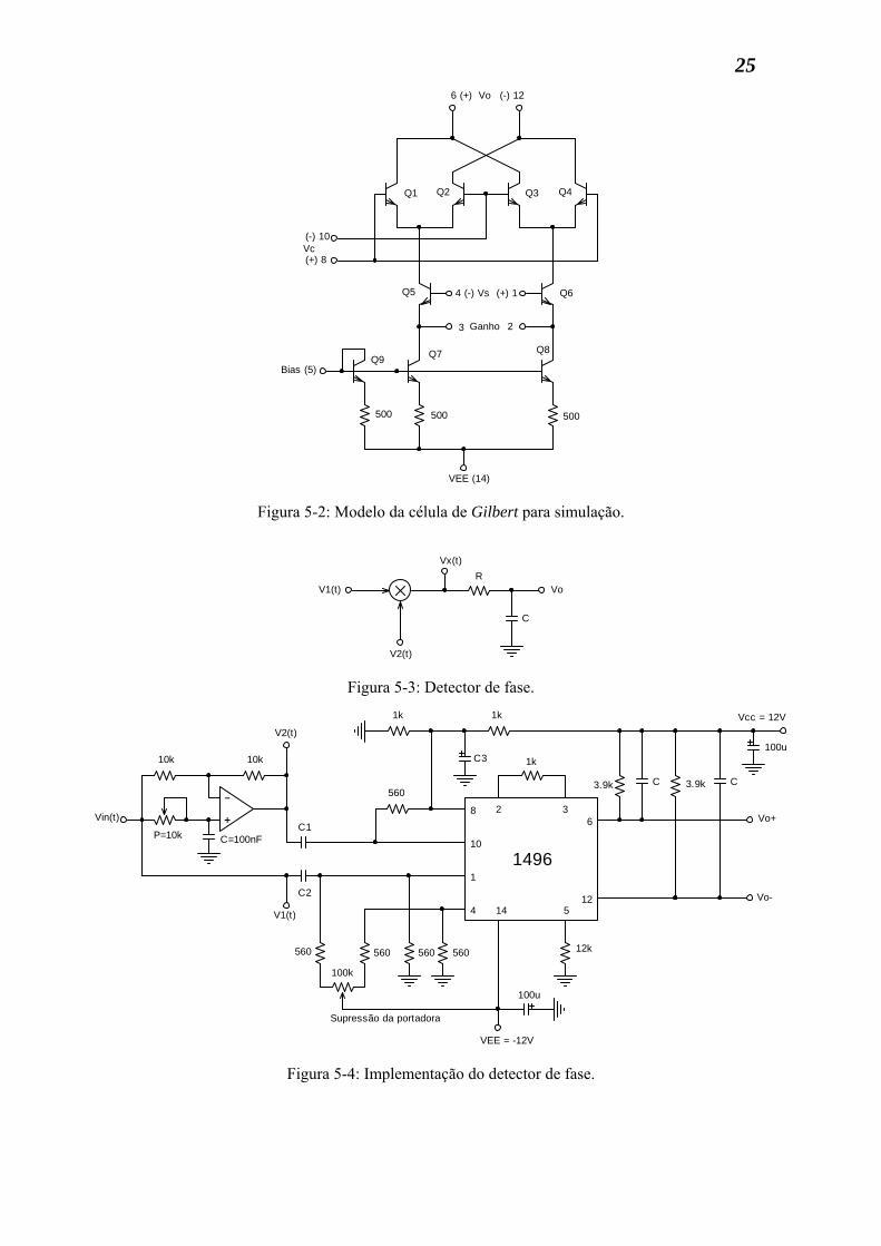
A presente prática será sobre os moduladores balanceados de transcondutância variável e com os co-letores dos diferenciais cruzados, conhecidos como células de Gilbert. Estas células são comuns a vários integrados como multiplicadores de quatro quadrantes, moduladores, etc. PROJETO Fase 1 - Projeto do modulador
Montar um circuito modulador em amplitude da Figura 5-1, que possa funcionar como AM DSB e AM DSB SC numa freqüência de portadora 32 100 10c rad sω π= × × e freqüência da moduladora
2m mfω π= , fm variando de 100Hz a 3kHz. Utilize o modelo da Figura 5-2 para realizar as simulações.
COMPONENTES CALCULADOS
C1= C2= C3=
POLARIZAÇÃO (com o potenciômetro a meio curso) Teórico Simulado Prático
V1= V8=
V2= V10=
V3= V12=
V4= V5=
V6=
V1= V8=
V2= V10=
V3= V12=
V4= V5=
V6=
V1= V8=
V2= V10=
V3= V12=
V4= V5=
V6=
22 Utilize como portadora uma onda senoidal de 100kHz com 100mV de amplitude, e uma senoide de 1kHz e 200mV de amplitude para a moduladora. Observe por simulação, e depois no osciloscópio, o sinal em Vo+ ou Vo-, que está modulado em amplitude e quase sem portadora.
ESBOCE O SINAL OBSERVADO EM Vo+ ou Vo- Simulado Prático
Varie o potenciômetro e observe a modulação mudar gradativamente de sem portadora para com portador.
ESBOCE O SINAL OBSERVADO EM Vo+ ou Vo-, COM ÍNDICE DE MODULAÇÃO Igual a 100% Igual a 50%
Ajuste o potenciômetro para obter índice de modulação de 100%. Varie a freqüência do sinal modulador e, observando a forma do sinal de saída, determine a freqüência de corte inferior do modulador.
FREQÜÊNCIA DE CORTE INFERIOR DO MODULADOR Teórico Prático
fCI = fCI =
COMENTÁRIOS SOBRE OS RESULTADOS OBTIDOS
23 Fase 2 - Duplicador de freqüência
O modulador balanceado pode ser usado, quando o sinal de entrada é senoidal, como duplicador, ou oitavador, de freqüência. Para isto, basta aplicar Vin simultaneamente às entradas portadora e moduladora. Desta forma, o sinal observado nas saídas Vo+ ou Vo- é proporcional a 2
inV , e pode ser representado como:
( ) ( ) ( )( )22 20 0sin 1 cos 2 2in m mV t V t V tω ω= = −
Ajuste o potenciômetro para que não exista portadora nas saídas Vo+ e Vo-, e aplique um sinal senoidal com 1kHz e 50mV de amplitude às entradas portadora e moduladora.
ESBOCE O SINAL OBSERVADO EM Vo+ ou Vo-, E ANOTE A FREQÜÊNCIA MEDIDA Teórico Simulado Prático
f = f = f =
COMENTÁRIOS SOBRE OS RESULTADOS OBTIDOS
Fase 3 - Detector de fase
O modulador balanceado pode ser usado como detector de fase, entre dois sinais de mesma freqüência, conforme a Figura 5-3. A tensão ( )oV t é o produto ( ) ( )1 2V t V t× , e considerando estas tensões senoidais, tem-se:
( ) ( ) ( ) ( ) ( )1 0 2 0 1 2 1 2 0sin sin cos 2 cos 2 2oV t V t V t VV VV tω ω θ θ ω θ= × + = − +
Calculando R e C para que formem um filtro passa-baixas, com freqüência de corte suficientemente pequena para eliminar a componente ( )1 2 0cos 2 2VV tω θ+ , obtém-se:
( ) ( )1 2 cos 2oV t VV θ≅
O circuito da Figura 5-4 utiliza um filtro passa-tudo para criar dois sinais defasados, V1(t) e V2(t), onde ( ) ( ) ( )1
2 1 2 tano o oV j V j PCω ω ω−− = − . Monte o circuito, e calcule os capacitores C para a freqüência de corte de 500Hz na saída. Ajuste o potenciômetro que controla a injeção de portadora para que
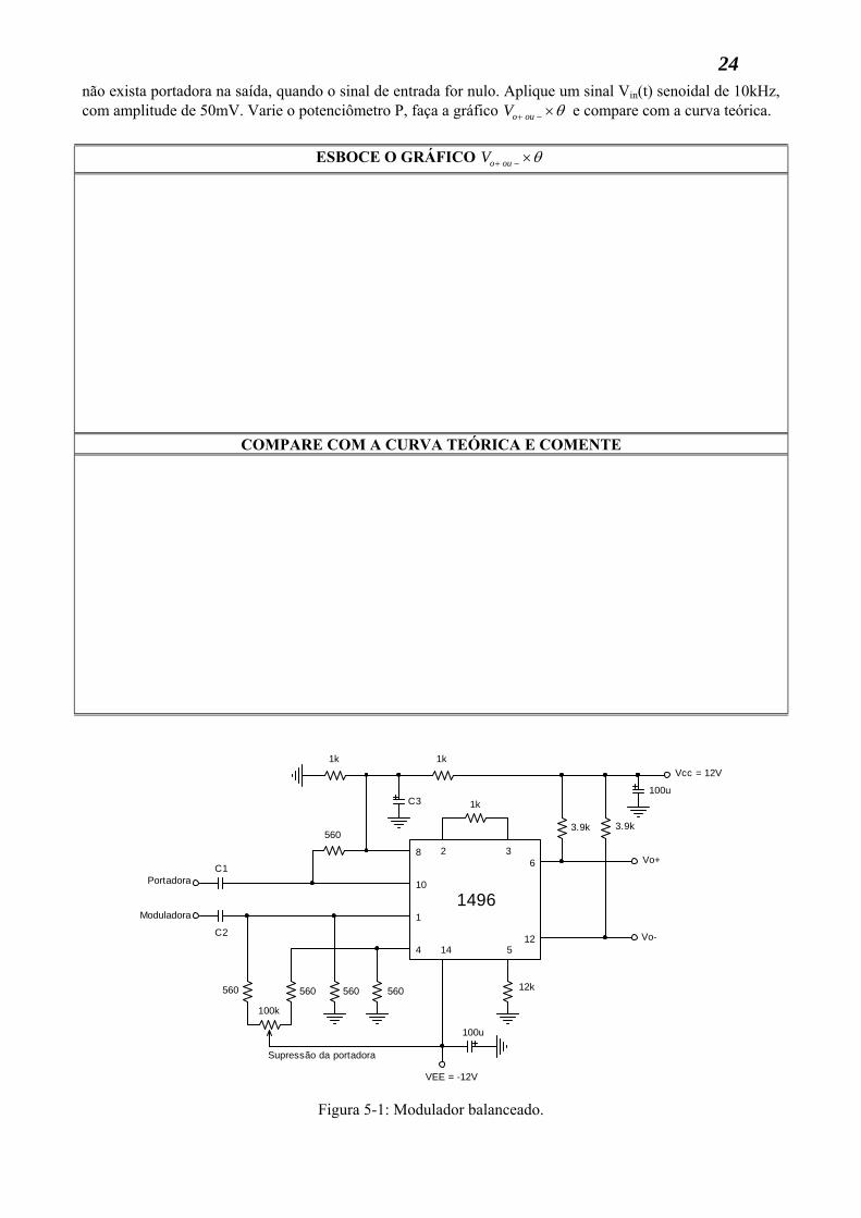
24 não exista portadora na saída, quando o sinal de entrada for nulo. Aplique um sinal Vin(t) senoidal de 10kHz, com amplitude de 50mV. Varie o potenciômetro P, faça a gráfico o ouV θ+ − × e compare com a curva teórica.
ESBOCE O GRÁFICO o ouV θ+ − ×
COMPARE COM A CURVA TEÓRICA E COMENTE
1k
1k1k
3.9k 3.9k
12k560 560560 560
100k
560
C1
C2
Vo+
Portadora
Vo-
Moduladora
VEE = -12V
100u
100uC3
Vcc = 12V
Supressão da portadora
1496
8
10
1
4
2 36
1214 5
Figura 5-1: Modulador balanceado.
25
Q1 Q2 Q3 Q4
Q5 Q6
Q7 Q8
500 500
Q9
500
(-) 10
(+) 8
(+) 14 (-)
Bias (5)
(-) 126 (+)
VEE (14)
3 2
Vs
Vc
Ganho
Vo
Figura 5-2: Modelo da célula de Gilbert para simulação.
R
C
V1(t)
V2(t)
Vo
Vx(t)
Figura 5-3: Detector de fase.
C=100nF
C C
1k
1k1k
3.9k 3.9k
12k560 560560 560
100k
560
C1
C2
Vin(t) Vo+
V2(t)
Vo-
VEE = -12V
100u
100uC3
Vcc = 12V
Supressão da portadora
1496
8
10
1
4
2 36
1214 5
+
-
10k 10k
P=10k
V1(t)
Figura 5-4: Implementação do detector de fase.
26
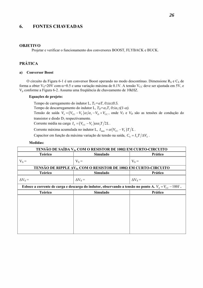
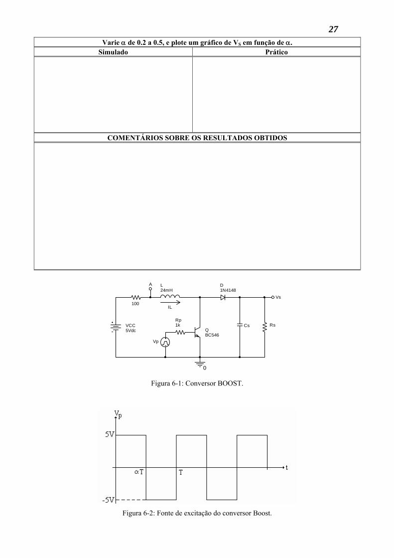
6. FONTES CHAVEADAS OBJETIVO Projetar e verificar o funcionamento dos conversores BOOST, FLYBACK e BUCK. PRÁTICA a) Conversor Boost O circuito da Figura 6-1 é um conversor Boost operando no modo descontínuo. Dimensione RS e CS de forma a obter VS=20V com α=0.5 e uma variação máxima de 0.1V. A tensão VCC deve ser ajustada em 5V, e Vp conforme a Figura 6-2. Assuma uma freqüência de chaveamento de 10kHZ.
Equações de projeto:
Tempo de carregamento do indutor L, TC=αT, 0≤α≤0.5. Tempo de descarregamento do indutor L, TD=α1T, 0≤α1≤(1-α). Tensão de saída ( ) 1S CC T D CCV V V V Vα α= − − + , onde VT e VD são as tensões de condução do transistor e diodo D1 respectivamente. Corrente média na carga ( ) 1 2S CC TI V V T Lαα= − . Corrente máxima acumulada no indutor L, ( )max CC TI V V T Lα= − . Capacitor em função da máxima variação de tensão na saída, S S SC I T V= ∆ .
Medidas:
TENSÃO DE SAÍDA VS, COM O RESISTOR DE 100Ω EM CURTO-CIRCUITO Teórico Simulado Prático
VS = VS = VS =
TENSÃO DE RIPPLE ∆VS, COM O RESISTOR DE 100Ω EM CURTO-CIRCUITO Teórico Simulado Prático
∆VS = ∆VS = ∆VS =
Esboce a corrente de carga e descarga do indutor, observando a tensão no ponto A. 100A CCV V I= − . Teórico Simulado Prático
27 Varie α de 0.2 a 0.5, e plote um gráfico de VS em função de α.
Simulado Prático
COMENTÁRIOS SOBRE OS RESULTADOS OBTIDOS
Rp1k
D1N4148
QBC546
L24mH
Cs
100
RsVCC5Vdc
Vp
0
A
Vs
IL
Figura 6-1: Conversor BOOST.
Figura 6-2: Fonte de excitação do conversor Boost.
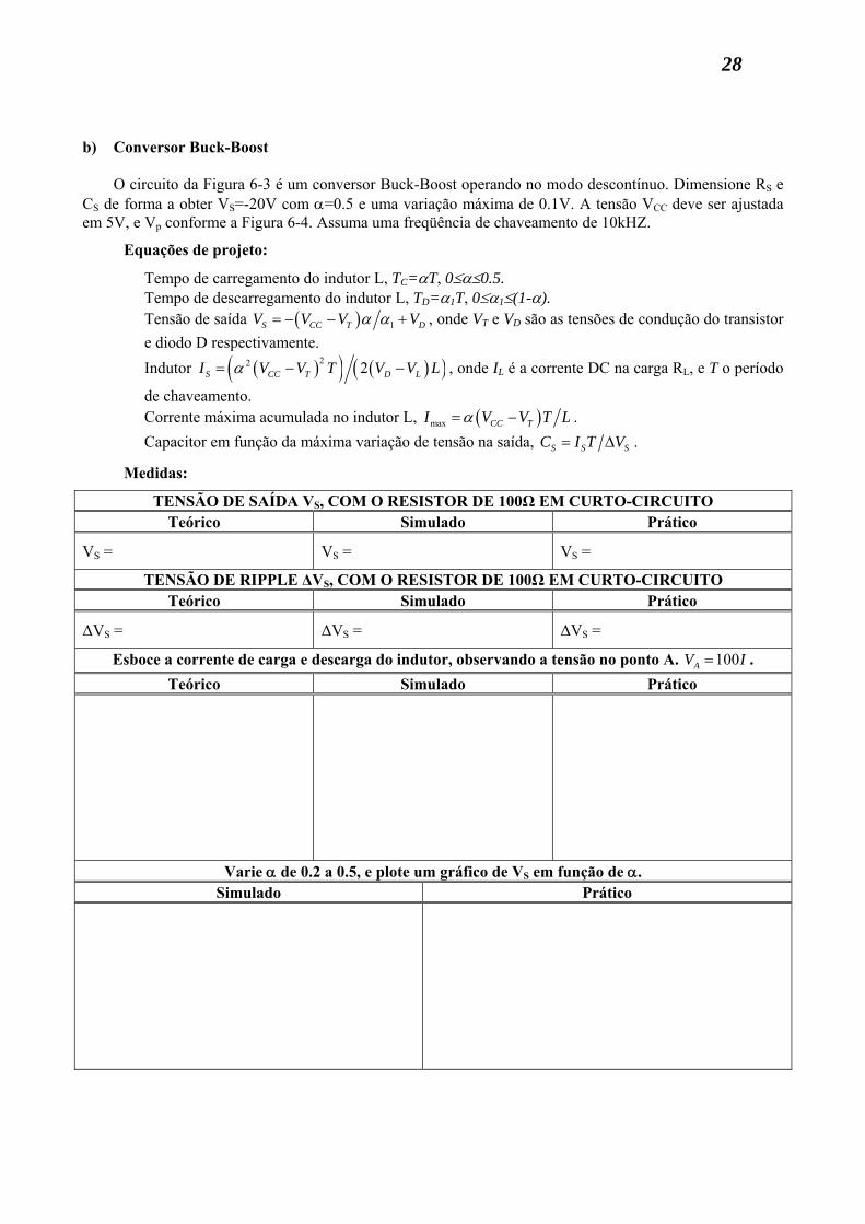
28 b) Conversor Buck-Boost O circuito da Figura 6-3 é um conversor Buck-Boost operando no modo descontínuo. Dimensione RS e CS de forma a obter VS=-20V com α=0.5 e uma variação máxima de 0.1V. A tensão VCC deve ser ajustada em 5V, e Vp conforme a Figura 6-4. Assuma uma freqüência de chaveamento de 10kHZ.
Equações de projeto:
Tempo de carregamento do indutor L, TC=αT, 0≤α≤0.5. Tempo de descarregamento do indutor L, TD=α1T, 0≤α1≤(1-α). Tensão de saída ( ) 1S CC T DV V V Vα α= − − + , onde VT e VD são as tensões de condução do transistor
e diodo D respectivamente. Indutor ( )( ) ( )( )22 2S CC T D LI V V T V V Lα= − − , onde IL é a corrente DC na carga RL, e T o período
de chaveamento. Corrente máxima acumulada no indutor L, ( )max CC TI V V T Lα= − . Capacitor em função da máxima variação de tensão na saída, S S SC I T V= ∆ .
Medidas:
TENSÃO DE SAÍDA VS, COM O RESISTOR DE 100Ω EM CURTO-CIRCUITO Teórico Simulado Prático
VS = VS = VS =
TENSÃO DE RIPPLE ∆VS, COM O RESISTOR DE 100Ω EM CURTO-CIRCUITO Teórico Simulado Prático
∆VS = ∆VS = ∆VS =
Esboce a corrente de carga e descarga do indutor, observando a tensão no ponto A. 100AV I= . Teórico Simulado Prático
Varie α de 0.2 a 0.5, e plote um gráfico de VS em função de α. Simulado Prático
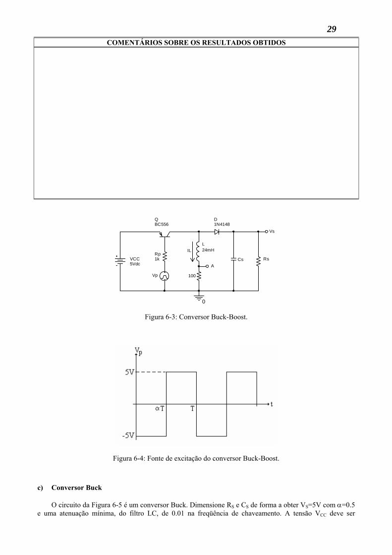
29 COMENTÁRIOS SOBRE OS RESULTADOS OBTIDOS
Rp1k
D1N4148
L24mH
Cs
100
RsVCC5Vdc
Vp
0
A
Vs
IL
QBC556
Figura 6-3: Conversor Buck-Boost.
Figura 6-4: Fonte de excitação do conversor Buck-Boost.
c) Conversor Buck O circuito da Figura 6-5 é um conversor Buck. Dimensione RS e CS de forma a obter VS=5V com α=0.5 e uma atenuação mínima, do filtro LC, de 0.01 na freqüência de chaveamento. A tensão VCC deve ser
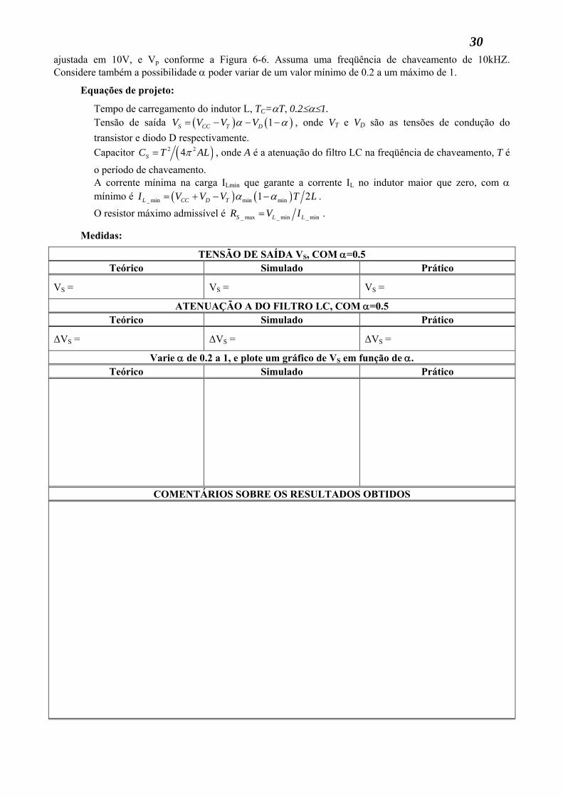
30 ajustada em 10V, e Vp conforme a Figura 6-6. Assuma uma freqüência de chaveamento de 10kHZ. Considere também a possibilidade α poder variar de um valor mínimo de 0.2 a um máximo de 1.
Equações de projeto:
Tempo de carregamento do indutor L, TC=αT, 0.2≤α≤1. Tensão de saída ( ) ( )1S CC T DV V V Vα α= − − − , onde VT e VD são as tensões de condução do transistor e diodo D respectivamente. Capacitor ( )2 24SC T ALπ= , onde A é a atenuação do filtro LC na freqüência de chaveamento, T é
o período de chaveamento. A corrente mínima na carga ILmin que garante a corrente IL no indutor maior que zero, com α mínimo é ( ) ( )_ min min min1 2L CC D TI V V V T Lα α= + − − . O resistor máximo admissível é _ max _ min _ minS L LR V I= .
Medidas:
TENSÃO DE SAÍDA VS, COM α=0.5 Teórico Simulado Prático
VS = VS = VS =
ATENUAÇÃO A DO FILTRO LC, COM α=0.5 Teórico Simulado Prático
∆VS = ∆VS = ∆VS =
Varie α de 0.2 a 1, e plote um gráfico de VS em função de α. Teórico Simulado Prático
COMENTÁRIOS SOBRE OS RESULTADOS OBTIDOS
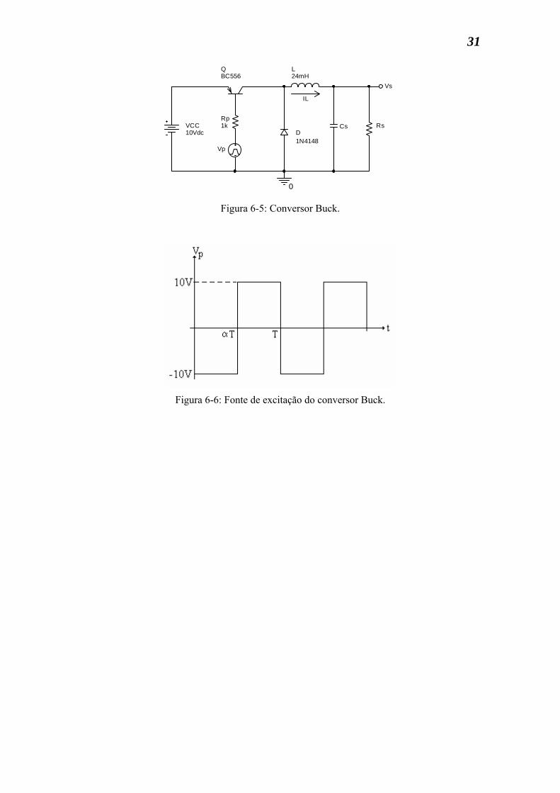
31
Rp1k
D1N4148
L24mH
Cs RsVCC10Vdc
Vp
0
Vs
IL
QBC556
Figura 6-5: Conversor Buck.
Figura 6-6: Fonte de excitação do conversor Buck.

32
DATASHEETS
1999 May 25 2
Philips Semiconductors Product specification
High-speed diodes 1N4148; 1N4448
FEATURES
• Hermetically sealed leaded glassSOD27 (DO-35) package
• High switching speed: max. 4 ns
• General application
• Continuous reverse voltage:max. 75 V
• Repetitive peak reverse voltage:max. 75 V
• Repetitive peak forward current:max. 450 mA.
APPLICATIONS
• High-speed switching.
DESCRIPTION
The 1N4148 and 1N4448 are high-speed switching diodes fabricated in planartechnology, and encapsulated in hermetically sealed leaded glass SOD27(DO-35) packages.
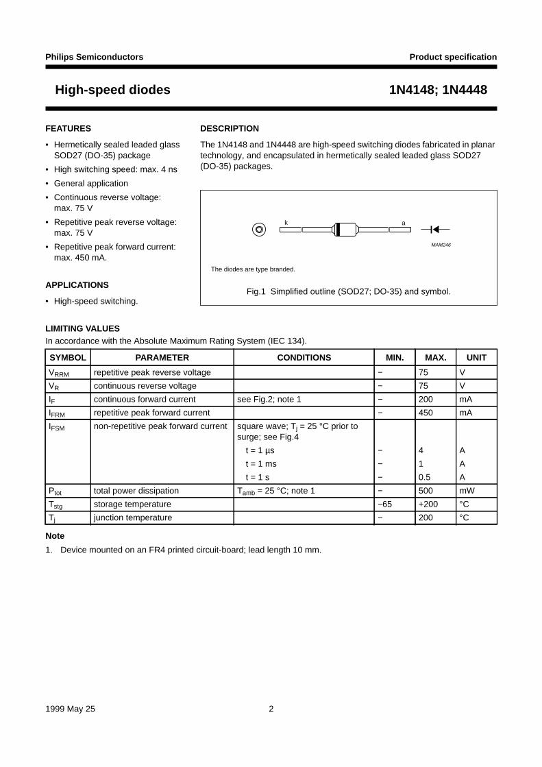
Fig.1 Simplified outline (SOD27; DO-35) and symbol.
The diodes are type branded.
handbook, halfpage
MAM246
k a
LIMITING VALUESIn accordance with the Absolute Maximum Rating System (IEC 134).
Note
1. Device mounted on an FR4 printed circuit-board; lead length 10 mm.
SYMBOL PARAMETER CONDITIONS MIN. MAX. UNIT
VRRM repetitive peak reverse voltage − 75 V
VR continuous reverse voltage − 75 V
IF continuous forward current see Fig.2; note 1 − 200 mA
IFRM repetitive peak forward current − 450 mA
IFSM non-repetitive peak forward current square wave; Tj = 25 °C prior tosurge; see Fig.4
t = 1 µs − 4 A
t = 1 ms − 1 A
t = 1 s − 0.5 A
Ptot total power dissipation Tamb = 25 °C; note 1 − 500 mW
Tstg storage temperature −65 +200 °CTj junction temperature − 200 °C
1999 May 25 3
Philips Semiconductors Product specification
High-speed diodes 1N4148; 1N4448
ELECTRICAL CHARACTERISTICSTj = 25 °C unless otherwise specified.
THERMAL CHARACTERISTICS
Note
1. Device mounted on a printed circuit-board without metallization pad.
SYMBOL PARAMETER CONDITIONS MIN. MAX. UNIT
VF forward voltage see Fig.3
1N4148 IF = 10 mA − 1 V
1N4448 IF = 5 mA 0.62 0.72 V
IF = 100 mA − 1 V
IR reverse current VR = 20 V; see Fig.5 25 nA
VR = 20 V; Tj = 150 °C; see Fig.5 − 50 µA
IR reverse current; 1N4448 VR = 20 V; Tj = 100 °C; see Fig.5 − 3 µA
Cd diode capacitance f = 1 MHz; VR = 0; see Fig.6 4 pF
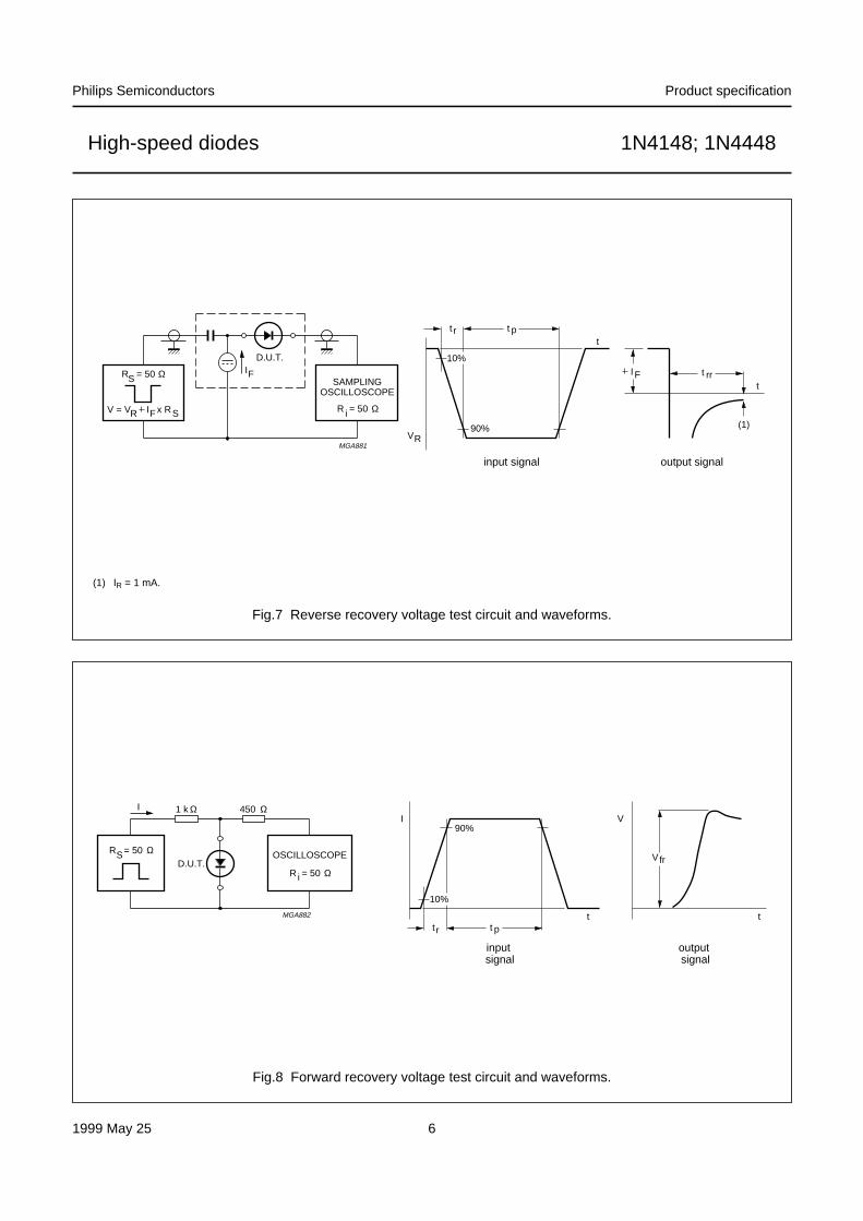
trr reverse recovery time when switched from IF = 10 mA toIR = 60 mA; RL = 100 Ω;measured at IR = 1 mA; see Fig.7
4 ns
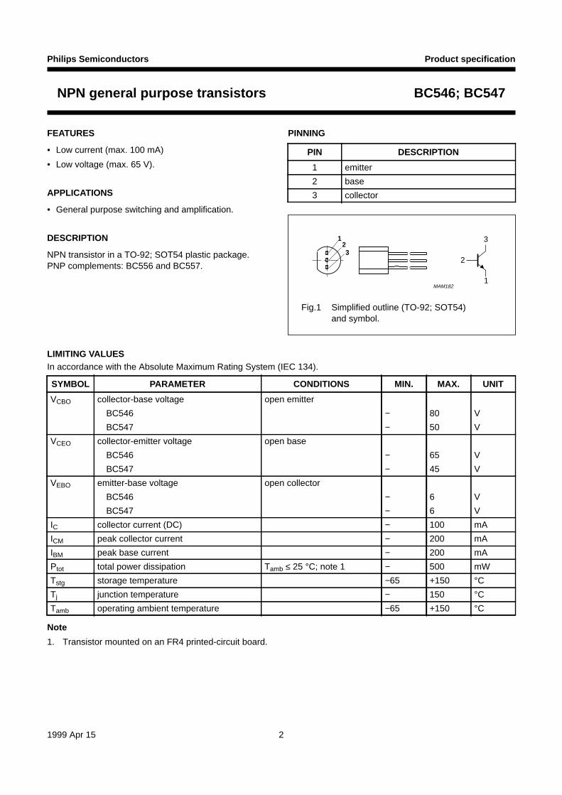
Vfr forward recovery voltage when switched from IF = 50 mA;tr = 20 ns; see Fig.8
− 2.5 V
SYMBOL PARAMETER CONDITIONS VALUE UNIT
Rth j-tp thermal resistance from junction to tie-point lead length 10 mm 240 K/W
Rth j-a thermal resistance from junction to ambient lead length 10 mm; note 1 350 K/W
1999 May 25 4
Philips Semiconductors Product specification
High-speed diodes 1N4148; 1N4448
GRAPHICAL DATA
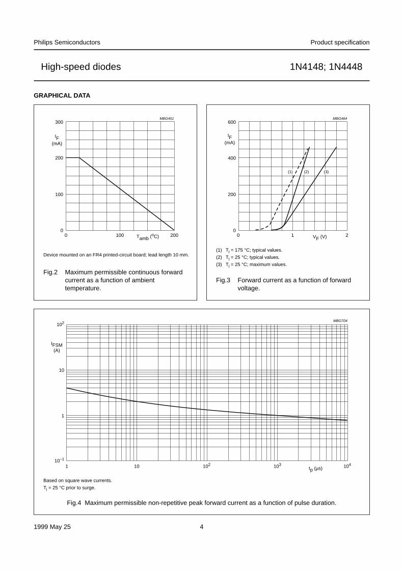
Fig.2 Maximum permissible continuous forwardcurrent as a function of ambienttemperature.
handbook, halfpage
0 100 200
300
200
0
100
MBG451
Tamb (oC)
IF(mA)
Device mounted on an FR4 printed-circuit board; lead length 10 mm.
Fig.3 Forward current as a function of forwardvoltage.
handbook, halfpage
0 1 2
600
0
200
400
MBG464
VF (V)
IF(mA)
(1) (2) (3)
(1) Tj = 175 °C; typical values.
(2) Tj = 25 °C; typical values.
(3) Tj = 25 °C; maximum values.
Fig.4 Maximum permissible non-repetitive peak forward current as a function of pulse duration.
Based on square wave currents.
Tj = 25 °C prior to surge.
handbook, full pagewidth
MBG704
10 tp (µs)1
IFSM(A)
102
10−1
104102 103
10
1
1999 May 25 5
Philips Semiconductors Product specification
High-speed diodes 1N4148; 1N4448
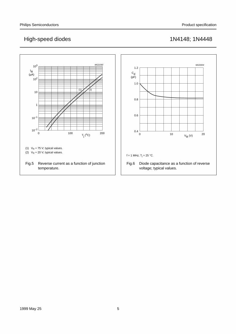
Fig.5 Reverse current as a function of junctiontemperature.
(1) VR = 75 V; typical values.
(2) VR = 20 V; typical values.
handbook, halfpage
0 100Tj (
oC)200
103
102
10−1
10−2
10(1)
1
IR(µA)
MGD290
(2)
Fig.6 Diode capacitance as a function of reversevoltage; typical values.
f = 1 MHz; Tj = 25 °C.
handbook, halfpage
0 10 20
1.2
1.0
0.6
0.4
0.8
MGD004
VR (V)
Cd(pF)
1999 May 25 6
Philips Semiconductors Product specification
High-speed diodes 1N4148; 1N4448
Fig.7 Reverse recovery voltage test circuit and waveforms.
handbook, full pagewidth
t rr
(1)
I Ft
output signal
t rt
t p
10%
90%VR
input signal
V = V I x RR F S
R = 50S Ω IF
D.U.T.
R = 50i Ω
SAMPLINGOSCILLOSCOPE
MGA881
(1) IR = 1 mA.
Fig.8 Forward recovery voltage test circuit and waveforms.
t rt
t p
10%
90%I
input signal
R = 50S Ω
I
R = 50i Ω
OSCILLOSCOPE
Ω1 k Ω450
D.U.T.
MGA882
Vfr
t
output signal
V
1999 Apr 15 2
Philips Semiconductors Product specification
NPN general purpose transistors BC546; BC547
FEATURES
• Low current (max. 100 mA)
• Low voltage (max. 65 V).
APPLICATIONS
• General purpose switching and amplification.
DESCRIPTION
NPN transistor in a TO-92; SOT54 plastic package.PNP complements: BC556 and BC557.
PINNING
PIN DESCRIPTION
1 emitter
2 base
3 collector
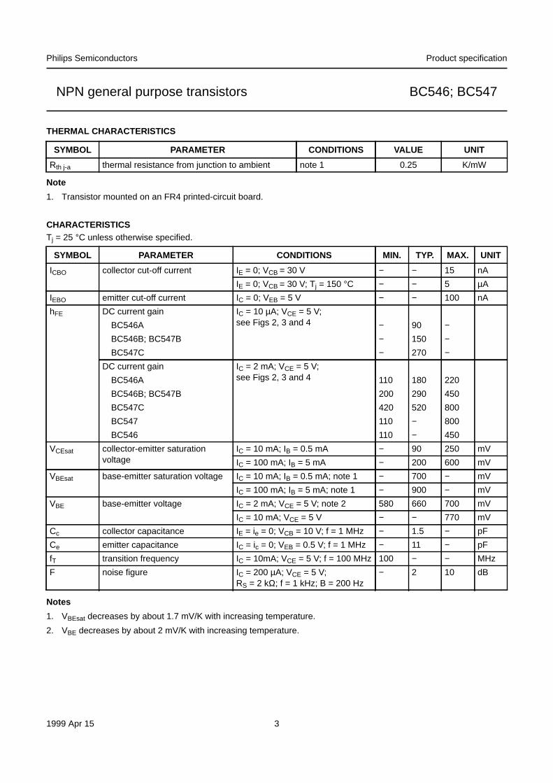
Fig.1 Simplified outline (TO-92; SOT54)and symbol.
handbook, halfpage1
32
MAM182
3
2
1
LIMITING VALUESIn accordance with the Absolute Maximum Rating System (IEC 134).
Note
1. Transistor mounted on an FR4 printed-circuit board.
SYMBOL PARAMETER CONDITIONS MIN. MAX. UNIT
VCBO collector-base voltage open emitter
BC546 − 80 V
BC547 − 50 V
VCEO collector-emitter voltage open base
BC546 − 65 V
BC547 − 45 V
VEBO emitter-base voltage open collector
BC546 − 6 V
BC547 − 6 V
IC collector current (DC) − 100 mA
ICM peak collector current − 200 mA
IBM peak base current − 200 mA
Ptot total power dissipation Tamb ≤ 25 °C; note 1 − 500 mW
Tstg storage temperature −65 +150 °CTj junction temperature − 150 °CTamb operating ambient temperature −65 +150 °C
1999 Apr 15 3
Philips Semiconductors Product specification
NPN general purpose transistors BC546; BC547
THERMAL CHARACTERISTICS
Note
1. Transistor mounted on an FR4 printed-circuit board.
CHARACTERISTICSTj = 25 °C unless otherwise specified.
Notes
1. VBEsat decreases by about 1.7 mV/K with increasing temperature.
2. VBE decreases by about 2 mV/K with increasing temperature.
SYMBOL PARAMETER CONDITIONS VALUE UNIT
Rth j-a thermal resistance from junction to ambient note 1 0.25 K/mW
SYMBOL PARAMETER CONDITIONS MIN. TYP. MAX. UNIT
ICBO collector cut-off current IE = 0; VCB = 30 V − − 15 nA
IE = 0; VCB = 30 V; Tj = 150 °C − − 5 µA
IEBO emitter cut-off current IC = 0; VEB = 5 V − − 100 nA
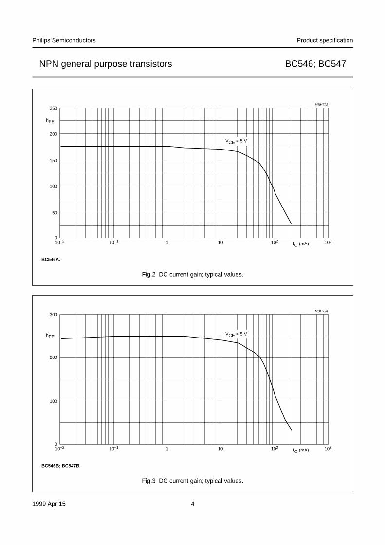
hFE DC current gain IC = 10 µA; VCE = 5 V;see Figs 2, 3 and 4BC546A − 90 −
BC546B; BC547B − 150 −BC547C − 270 −
DC current gain IC = 2 mA; VCE = 5 V;see Figs 2, 3 and 4BC546A 110 180 220
BC546B; BC547B 200 290 450
BC547C 420 520 800
BC547 110 − 800
BC546 110 − 450
VCEsat collector-emitter saturationvoltage
IC = 10 mA; IB = 0.5 mA − 90 250 mV
IC = 100 mA; IB = 5 mA − 200 600 mV
VBEsat base-emitter saturation voltage IC = 10 mA; IB = 0.5 mA; note 1 − 700 − mV
IC = 100 mA; IB = 5 mA; note 1 − 900 − mV
VBE base-emitter voltage IC = 2 mA; VCE = 5 V; note 2 580 660 700 mV
IC = 10 mA; VCE = 5 V − − 770 mV
Cc collector capacitance IE = ie = 0; VCB = 10 V; f = 1 MHz − 1.5 − pF
Ce emitter capacitance IC = ic = 0; VEB = 0.5 V; f = 1 MHz − 11 − pF
fT transition frequency IC = 10mA; VCE = 5 V; f = 100 MHz 100 − − MHz
F noise figure IC = 200 µA; VCE = 5 V;RS = 2 kΩ; f = 1 kHz; B = 200 Hz
− 2 10 dB
1999 Apr 15 4
Philips Semiconductors Product specification
NPN general purpose transistors BC546; BC547
Fig.2 DC current gain; typical values.
handbook, full pagewidth
0
250
50
100
150
200
MBH723
10−2 10−1
hFE
1 IC (mA)10 103102
VCE = 5 V
BC546A.
Fig.3 DC current gain; typical values.
handbook, full pagewidth
0
300
100
200
MBH724
10−2 10−1
hFE
1 IC (mA)10 103102
VCE = 5 V
BC546B; BC547B.
1999 Apr 15 5
Philips Semiconductors Product specification
NPN general purpose transistors BC546; BC547
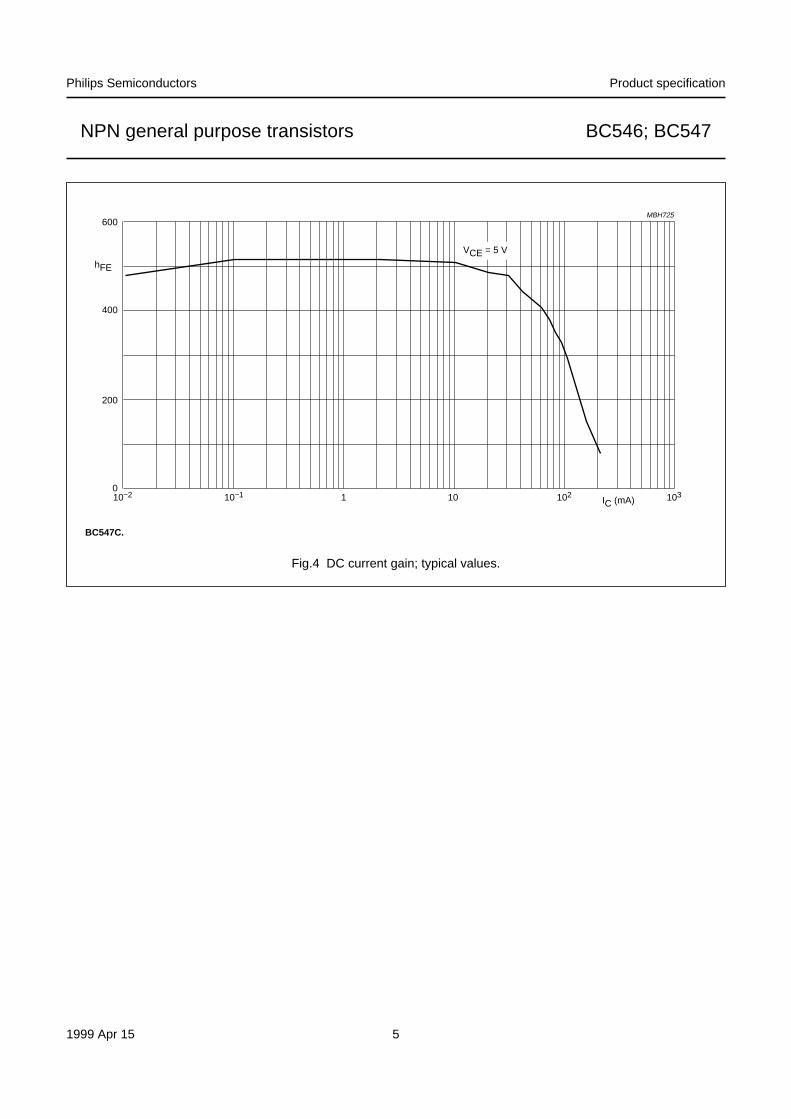
Fig.4 DC current gain; typical values.
handbook, full pagewidth
0
600
200
400
MBH725
10−2 10−1
hFE
1 IC (mA)10 103102
VCE = 5 V
BC547C.
1999 Apr 15 2
Philips Semiconductors Product specification
PNP general purpose transistors BC556; BC557
FEATURES
• Low current (max. 100 mA)
• Low voltage (max. 65 V).
APPLICATIONS
• General purpose switching and amplification.
DESCRIPTION
PNP transistor in a TO-92; SOT54 plastic package.NPN complements: BC546 and BC547.
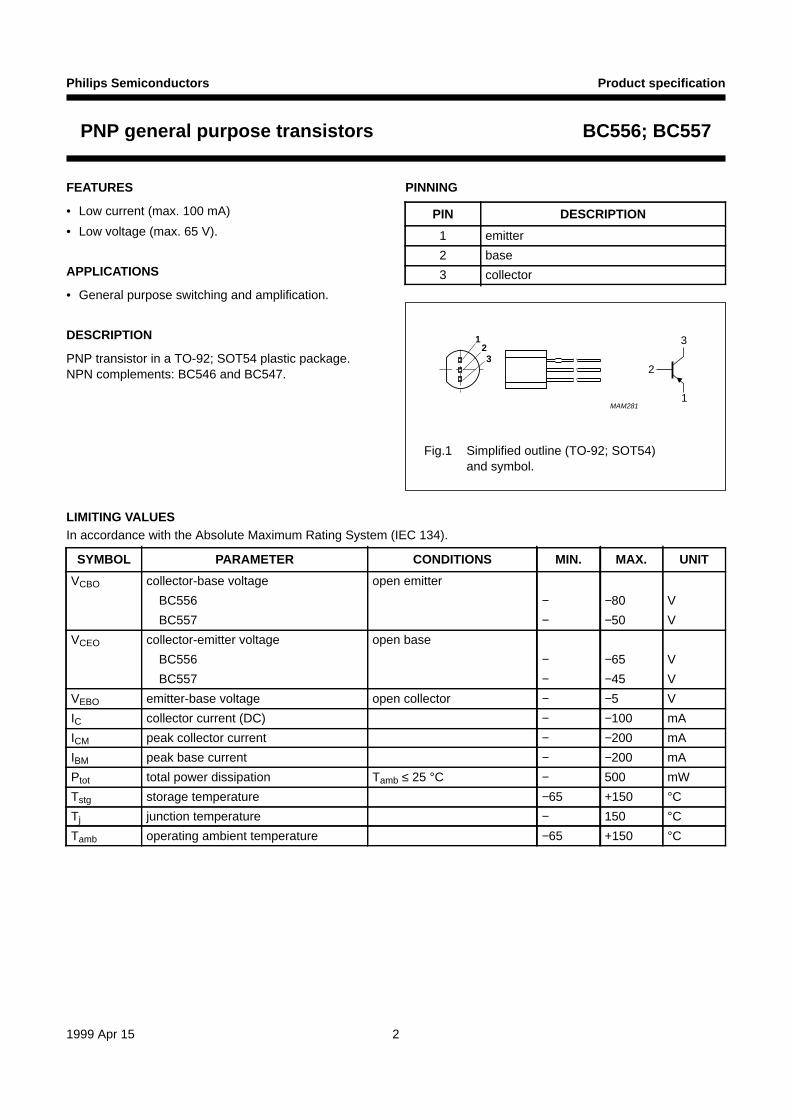
PINNING
PIN DESCRIPTION
1 emitter
2 base
3 collector
Fig.1 Simplified outline (TO-92; SOT54)and symbol.
handbook, halfpage1
32
MAM281
3
2
1
LIMITING VALUESIn accordance with the Absolute Maximum Rating System (IEC 134).
SYMBOL PARAMETER CONDITIONS MIN. MAX. UNIT
VCBO collector-base voltage open emitter
BC556 − −80 V
BC557 − −50 V
VCEO collector-emitter voltage open base
BC556 − −65 V
BC557 − −45 V
VEBO emitter-base voltage open collector − −5 V
IC collector current (DC) − −100 mA
ICM peak collector current − −200 mA
IBM peak base current − −200 mA
Ptot total power dissipation Tamb ≤ 25 °C − 500 mW
Tstg storage temperature −65 +150 °CTj junction temperature − 150 °CTamb operating ambient temperature −65 +150 °C
1999 Apr 15 3
Philips Semiconductors Product specification
PNP general purpose transistors BC556; BC557
THERMAL CHARACTERISTICS
Note
1. Transistor mounted on an FR4 printed-circuit board.
CHARACTERISTICSTj = 25 °C unless otherwise specified.
Notes
1. VBEsat decreases by about −1.7 mV/K with increasing temperature.
2. VBE decreases by about −2 mV/K with increasing temperature.
SYMBOL PARAMETER CONDITIONS VALUE UNIT
Rth j-a thermal resistance from junction to ambient note 1 250 K/W
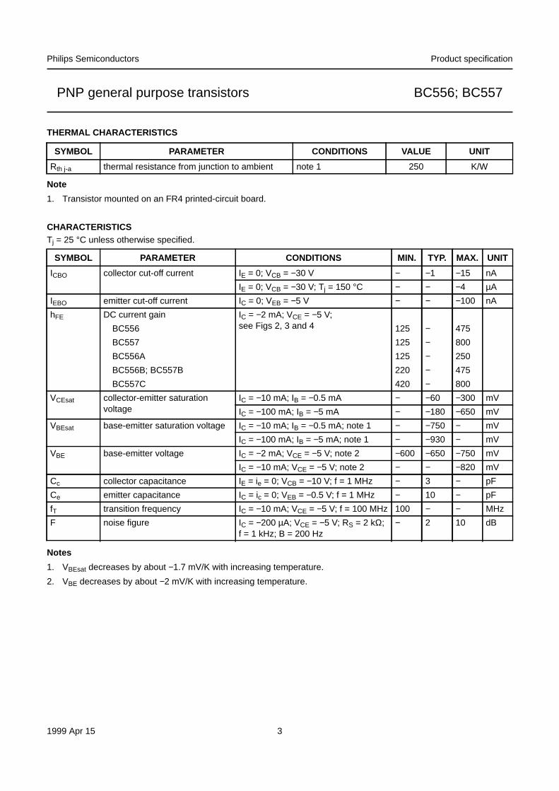
SYMBOL PARAMETER CONDITIONS MIN. TYP. MAX. UNIT
ICBO collector cut-off current IE = 0; VCB = −30 V − −1 −15 nA
IE = 0; VCB = −30 V; Tj = 150 °C − − −4 µA
IEBO emitter cut-off current IC = 0; VEB = −5 V − − −100 nA
hFE DC current gain IC = −2 mA; VCE = −5 V;see Figs 2, 3 and 4BC556 125 − 475
BC557 125 − 800
BC556A 125 − 250
BC556B; BC557B 220 − 475
BC557C 420 − 800
VCEsat collector-emitter saturationvoltage
IC = −10 mA; IB = −0.5 mA − −60 −300 mV
IC = −100 mA; IB = −5 mA − −180 −650 mV
VBEsat base-emitter saturation voltage IC = −10 mA; IB = −0.5 mA; note 1 − −750 − mV
IC = −100 mA; IB = −5 mA; note 1 − −930 − mV
VBE base-emitter voltage IC = −2 mA; VCE = −5 V; note 2 −600 −650 −750 mV
IC = −10 mA; VCE = −5 V; note 2 − − −820 mV
Cc collector capacitance IE = ie = 0; VCB = −10 V; f = 1 MHz − 3 − pF
Ce emitter capacitance IC = ic = 0; VEB = −0.5 V; f = 1 MHz − 10 − pF
fT transition frequency IC = −10 mA; VCE = −5 V; f = 100 MHz 100 − − MHz
F noise figure IC = −200 µA; VCE = −5 V; RS = 2 kΩ;f = 1 kHz; B = 200 Hz
− 2 10 dB
1999 Apr 15 4
Philips Semiconductors Product specification
PNP general purpose transistors BC556; BC557
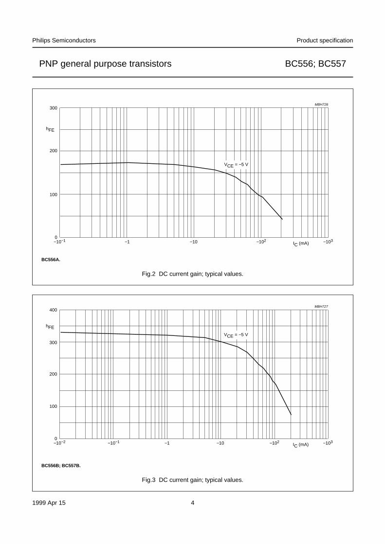
Fig.2 DC current gain; typical values.
handbook, full pagewidth
0
300
100
200
MBH726
−10−1
hFE
−1 IC (mA)−10 −103−102
VCE = −5 V
BC556A.
Fig.3 DC current gain; typical values.
handbook, full pagewidth
0
300
200
100
400MBH727
−10−2 −10−1
hFE
−1 IC (mA)−10 −103−102
VCE = −5 V
BC556B; BC557B.
1999 Apr 15 5
Philips Semiconductors Product specification
PNP general purpose transistors BC556; BC557
Fig.4 DC current gain; typical values.
handbook, full pagewidth
0
300
200
100
600
500
400
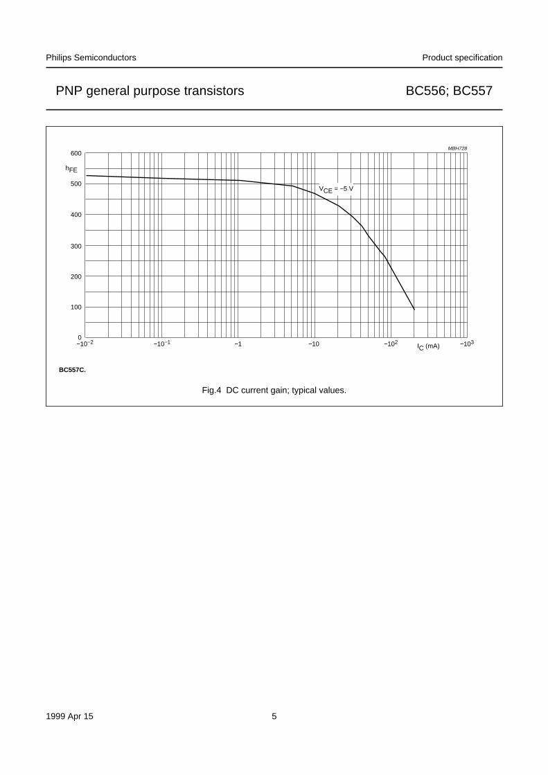
MBH728
−10−2 −10−1
hFE
−1 IC (mA)−10 −103−102
VCE = −5 V
BC557C.
1997 Jul 08 2
Philips Semiconductors Product specification
NPN medium frequency transistors BF494; BF495
FEATURES
• Low current (max. 30 mA)
• Low voltage (max. 20 V).
APPLICATIONS
• HF applications in radio and television receivers
• FM tuners
• Low noise AM mixer-oscillators
• IF amplifiers in AM/FM receivers.
DESCRIPTION
NPN medium frequency transistor in a TO-92; SOT54plastic package.
PINNING
PIN DESCRIPTION
1 base
2 emitter
3 collector
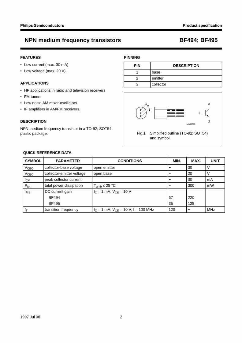
Fig.1 Simplified outline (TO-92; SOT54)and symbol.
handbook, halfpage1
32
MAM258
3
1
2
QUICK REFERENCE DATA
SYMBOL PARAMETER CONDITIONS MIN. MAX. UNIT
VCBO collector-base voltage open emitter − 30 V
VCEO collector-emitter voltage open base − 20 V
ICM peak collector current − 30 mA
Ptot total power dissipation Tamb ≤ 25 °C − 300 mW
hFE DC current gain IC = 1 mA; VCE = 10 V
BF494 67 220
BF495 35 125
fT transition frequency IC = 1 mA; VCE = 10 V; f = 100 MHz 120 − MHz
1997 Jul 08 3
Philips Semiconductors Product specification
NPN medium frequency transistors BF494; BF495
LIMITING VALUESIn accordance with the Absolute Maximum Rating System (IEC 134).
Note
1. Transistor mounted on an FR4 printed-circuit board.
THERMAL CHARACTERISTICS
Note
1. Transistor mounted on an FR4 printed-circuit board.
CHARACTERISTICSTamb = 25 °C unless otherwise specified.
SYMBOL PARAMETER CONDITIONS MIN. MAX. UNIT
VCBO collector-base voltage open emitter − 30 V
VCEO collector-emitter voltage open base − 20 V
VEBO emitter-base voltage open collector − 5 V
IC collector current (DC) − 30 mA
ICM peak collector current − 30 mA
Ptot total power dissipation Tamb ≤ 25 °C; note 1 − 300 mW
Tstg storage temperature −65 +150 °CTj junction temperature − 150 °CTamb operating ambient temperature −65 +150 °C
SYMBOL PARAMETER CONDITIONS VALUE UNIT
Rth j-a thermal resistance from junction to ambient note 1 420 K/W
SYMBOL PARAMETER CONDITIONS MIN. MAX. UNIT
ICBO collector cut-off current IE = 0; VCB = 20 V − 100 nA
IE = 0; VCB = 20 V; Tamb = 150 °C − 4 µA
IEBO emitter cut-off current IC = 0; VEB = 4 V − 100 nA
hFE DC current gain IC = 1 mA; VCE = 10 V
BF494 67 220
BF494B 100 220
BF495 35 125
BF495B 100 125
VBE base-emitter voltage IC = 1 mA; VCE = 10 V 650 740 mV
Cre feedback capacitance IC = 0; VCB = 10 V; f = 1 MHz − 1 pF
fT transition frequency IC = 1 mA; VCE = 10 V; f = 100 MHz 120 − MHz
TIP29, TIP29A, TIP29B, TIP29CNPN SILICON POWER TRANSISTORS
P R O D U C T I N F O R M A T I O N
1
JULY 1968 - REVISED MARCH 1997Copyright © 1997, Power Innovations Limited, UK
Information is current as of publication date. Products conform to specifications in accordancewith the terms of Power Innovations standard warranty. Production processing does notnecessarily include testing of all parameters.
Designed for Complementary Use with the TIP30 Series
30 W at 25°C Case Temperature
1 A Continuous Collector Current
3 A Peak Collector Current
Customer-Specified Selections Available
B
C
E
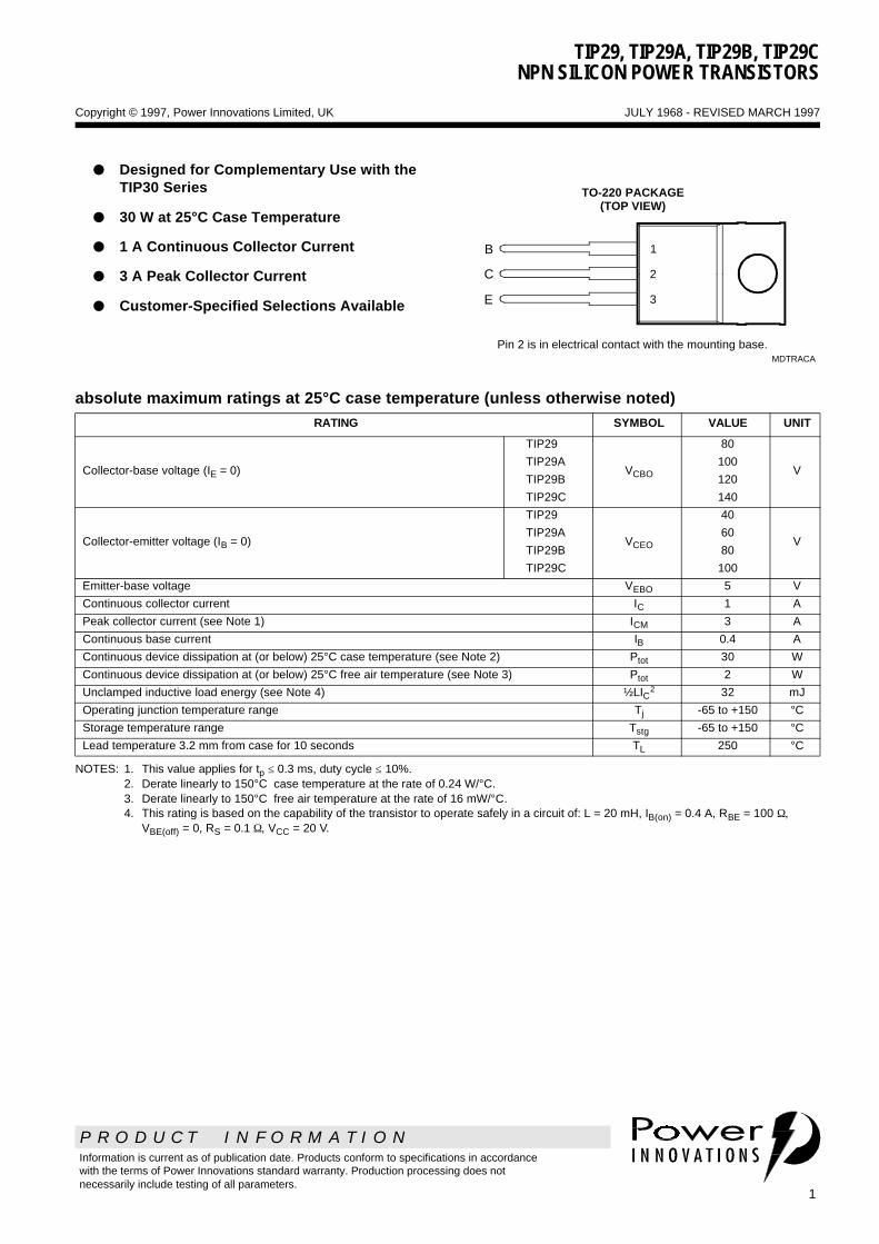
TO-220 PACKAGE(TOP VIEW)
Pin 2 is in electrical contact with the mounting base.MDTRACA
1
2
3
absolute maximum ratings at 25°C case temperature (unless otherwise noted)
NOTES: 1. This value applies for tp ≤ 0.3 ms, duty cycle ≤ 10%.2. Derate linearly to 150°C case temperature at the rate of 0.24 W/°C.3. Derate linearly to 150°C free air temperature at the rate of 16 mW/°C.4. This rating is based on the capability of the transistor to operate safely in a circuit of: L = 20 mH, IB(on) = 0.4 A, RBE = 100 Ω,
VBE(off) = 0, RS = 0.1 Ω, VCC = 20 V.
RATING SYMBOL VALUE UNIT
Collector-base voltage (IE = 0)
TIP29
TIP29A
TIP29B
TIP29C
VCBO
80
100
120
140
V
Collector-emitter voltage (IB = 0)
TIP29
TIP29A
TIP29B
TIP29C
VCEO
40
60
80
100
V
Emitter-base voltage VEBO 5 V
Continuous collector current IC 1 A
Peak collector current (see Note 1) ICM 3 A
Continuous base current IB 0.4 A
Continuous device dissipation at (or below) 25°C case temperature (see Note 2) Ptot 30 W
Continuous device dissipation at (or below) 25°C free air temperature (see Note 3) Ptot 2 W
Unclamped inductive load energy (see Note 4) ½LIC2 32 mJ
Operating junction temperature range Tj -65 to +150 °C
Storage temperature range Tstg -65 to +150 °C
Lead temperature 3.2 mm from case for 10 seconds TL 250 °C

TIP29, TIP29A, TIP29B, TIP29CNPN SILICON POWER TRANSISTORS
2
JULY 1968 - REVISED MARCH 1997
P R O D U C T I N F O R M A T I O N
NOTES: 5. These parameters must be measured using pulse techniques, tp = 300 µs, duty cycle ≤ 2%.6. These parameters must be measured using voltage-sensing contacts, separate from the current carrying contacts.
† Voltage and current values shown are nominal; exact values vary slightly with transistor parameters.
electrical characteristics at 25°C case temperature
PARAMETER TEST CONDITIONS MIN TYP MAX UNIT
V(BR)CEOCollector-emitter
breakdown voltageIC = 30 mA
(see Note 5)
IB = 0
TIP29
TIP29A
TIP29B
TIP29C
40
60
80
100
V
ICESCollector-emitter
cut-off current
VCE = 80 V
VCE = 100 V
VCE = 120 V
VCE = 140 V
VBE = 0
VBE = 0
VBE = 0
VBE = 0
TIP29
TIP29A
TIP29B
TIP29C
0.2
0.2
0.2
0.2
mA
ICEOCollector cut-off
current
VCE = 30 V
VCE = 60 V
IB = 0
IB = 0
TIP29/29A
TIP29B/29C
0.3
0.3mA
IEBOEmitter cut-off
currentVEB = 5 V IC = 0 1 mA
hFEForward current
transfer ratio
VCE = 4 V
VCE = 4 V
IC = 0.2 A
IC = 1 A(see Notes 5 and 6)
40
15 75
VCE(sat)Collector-emitter
saturation voltageIB = 125 mA IC = 1 A (see Notes 5 and 6) 0.7 V
VBEBase-emitter
voltageVCE = 4 V IC = 1 A (see Notes 5 and 6) 1.3 V
hfeSmall signal forward
current transfer ratioVCE = 10 V IC = 0.2 A f = 1 kHz 20
|hfe|Small signal forward
current transfer ratioVCE = 10 V IC = 0.2 A f = 1 MHz 3
thermal characteristics
PARAMETER MIN TYP MAX UNIT
RθJC Junction to case thermal resistance 4.17 °C/W
RθJA Junction to free air thermal resistance 62.5 °C/W
resistive-load-switching characteristics at 25°C case temperature
PARAMETER TEST CONDITIONS † MIN TYP MAX UNIT
ton Turn-on time IC = 1 A
VBE(off) = -4.3 V
IB(on) = 0.1 A
RL = 30 Ω
IB(off) = -0.1 A
tp = 20 µs, dc ≤ 2%
0.5 µs
toff Turn-off time 2 µs
3
JULY 1968 - REVISED MARCH 1997
TIP29, TIP29A, TIP29B, TIP29CNPN SILICON POWER TRANSISTORS
P R O D U C T I N F O R M A T I O N
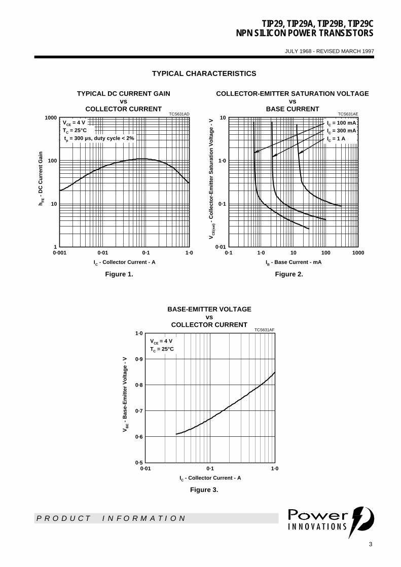
TYPICAL CHARACTERISTICS
Figure 1. Figure 2.
Figure 3.
TYPICAL DC CURRENT GAINvs
COLLECTOR CURRENT
IC - Collector Current - A
0·001 0·01 0·1 1·0
hF
E -
DC
Cu
rren
t G
ain
1
10
100
1000TCS631AD
VCE = 4 VTC = 25°C tp = 300 µs, duty cycle < 2%
COLLECTOR-EMITTER SATURATION VOLTAGEvs
BASE CURRENT
IB - Base Current - mA
0·1 1·0 10 100 1000
VC
E(s
at) -
Co
llect
or-
Em
itte
r S
atu
rati
on
Vo
ltag
e -
V
0·01
0·1
1·0
10TCS631AE
IC = 100 mAIC = 300 mAIC = 1 A
BASE-EMITTER VOLTAGEvs
COLLECTOR CURRENT
IC - Collector Current - A
0·01 0·1 1·0
VB
E -
Bas
e-E
mit
ter
Vo
ltag
e -
V
0·5
0·6
0·7
0·8
0·9
1·0TCS631AF
VCE = 4 VTC = 25°C
TIP29, TIP29A, TIP29B, TIP29CNPN SILICON POWER TRANSISTORS
4
JULY 1968 - REVISED MARCH 1997
P R O D U C T I N F O R M A T I O N
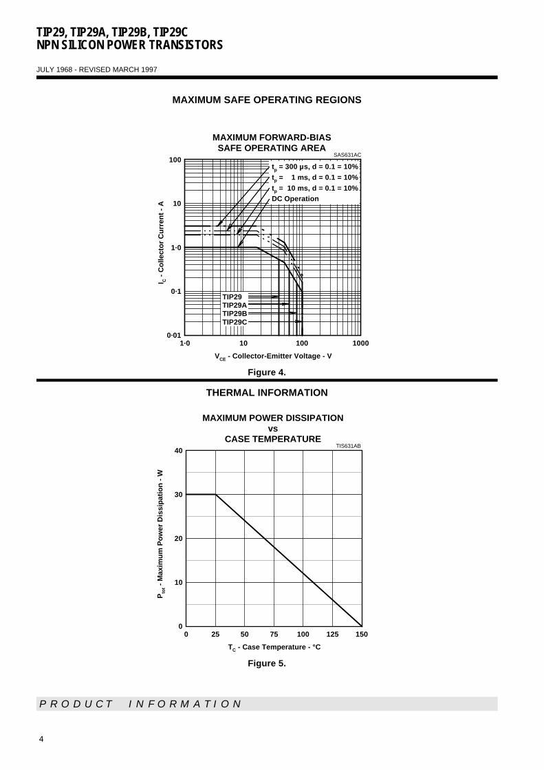
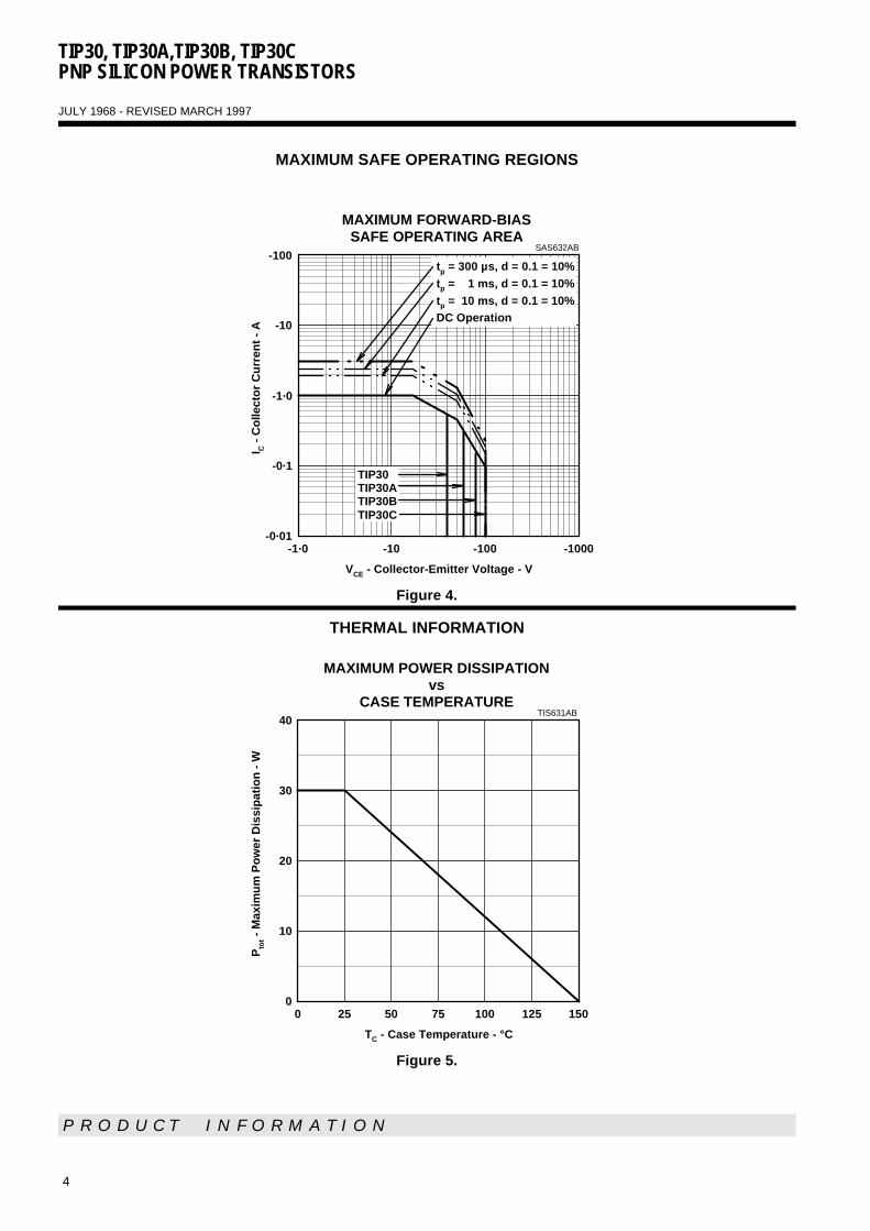
MAXIMUM SAFE OPERATING REGIONS
Figure 4.
THERMAL INFORMATION
Figure 5.
MAXIMUM FORWARD-BIASSAFE OPERATING AREA
VCE - Collector-Emitter Voltage - V
1·0 10 100 1000
I C -
Co
llect
or
Cu
rren
t -
A
0·01
0·1
1·0
10
100SAS631AC
TIP29TIP29ATIP29BTIP29C
tp = 300 µs, d = 0.1 = 10%tp = 1 ms, d = 0.1 = 10%tp = 10 ms, d = 0.1 = 10%DC Operation
MAXIMUM POWER DISSIPATIONvs
CASE TEMPERATURE
TC - Case Temperature - °C
0 25 50 75 100 125 150
Pto
t - M
axim
um
Po
wer
Dis
sip
atio
n -
W
0
10
20
30
40TIS631AB

TIP30, TIP30A,TIP30B, TIP30CPNP SILICON POWER TRANSISTORS
P R O D U C T I N F O R M A T I O N
1
JULY 1968 - REVISED MARCH 1997Copyright © 1997, Power Innovations Limited, UK
Information is current as of publication date. Products conform to specifications in accordancewith the terms of Power Innovations standard warranty. Production processing does notnecessarily include testing of all parameters.
Designed for Complementary Use with the TIP29 Series
30 W at 25°C Case Temperature
1 A Continuous Collector Current
3 A Peak Collector Current
Customer-Specified Selections Available
B
C
E
TO-220 PACKAGE(TOP VIEW)
Pin 2 is in electrical contact with the mounting base.MDTRACA
1
2
3
absolute maximum ratings at 25°C case temperature (unless otherwise noted)
NOTES: 1. This value applies for tp ≤ 0.3 ms, duty cycle ≤ 10%.2. Derate linearly to 150°C case temperature at the rate of 0.24 W/°C.3. Derate linearly to 150°C free air temperature at the rate of 16 mW/°C.4. This rating is based on the capability of the transistor to operate safely in a circuit of: L = 20 mH, IB(on) = -0.4 A, RBE = 100 Ω,
VBE(off) = 0, RS = 0.1 Ω, VCC = -20 V.
RATING SYMBOL VALUE UNIT
Collector-base voltage (IE = 0)
TIP30
TIP30A
TIP30B
TIP30C
VCBO
-80
-100
-120
-140
V
Collector-emitter voltage (IB = 0)
TIP30
TIP30A
TIP30B
TIP30C
VCEO
-40
-60
-80
-100
V
Emitter-base voltage VEBO -5 V
Continuous collector current IC -1 A
Peak collector current (see Note 1) ICM -3 A
Continuous base current IB -0.4 A
Continuous device dissipation at (or below) 25°C case temperature (see Note 2) Ptot 30 W
Continuous device dissipation at (or below) 25°C free air temperature (see Note 3) Ptot 2 W
Unclamped inductive load energy (see Note 4) ½LIC2 32 mJ
Operating junction temperature range Tj -65 to +150 °C
Storage temperature range Tstg -65 to +150 °C
Lead temperature 3.2 mm from case for 10 seconds TL 250 °C
TIP30, TIP30A,TIP30B, TIP30CPNP SILICON POWER TRANSISTORS
2
JULY 1968 - REVISED MARCH 1997
P R O D U C T I N F O R M A T I O N
NOTES: 5. These parameters must be measured using pulse techniques, tp = 300 µs, duty cycle ≤ 2%.6. These parameters must be measured using voltage-sensing contacts, separate from the current carrying contacts.
† Voltage and current values shown are nominal; exact values vary slightly with transistor parameters.
electrical characteristics at 25°C case temperature
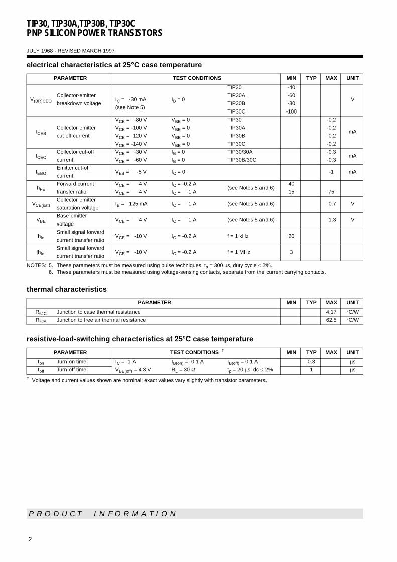
PARAMETER TEST CONDITIONS MIN TYP MAX UNIT
V(BR)CEOCollector-emitter
breakdown voltageIC = -30 mA
(see Note 5)
IB = 0
TIP30
TIP30A
TIP30B
TIP30C
-40
-60
-80
-100
V
ICESCollector-emitter
cut-off current
VCE = -80 V
VCE = -100 V
VCE = -120 V
VCE = -140 V
VBE = 0
VBE = 0
VBE = 0
VBE = 0
TIP30
TIP30A
TIP30B
TIP30C
-0.2
-0.2
-0.2
-0.2
mA
ICEOCollector cut-off
current
VCE = -30 V
VCE = -60 V
IB = 0
IB = 0
TIP30/30A
TIP30B/30C
-0.3
-0.3mA
IEBOEmitter cut-off
currentVEB = -5 V IC = 0 -1 mA
hFEForward current
transfer ratio
VCE = -4 V
VCE = -4 V
IC = -0.2 A
IC = -1 A(see Notes 5 and 6)
40
15 75
VCE(sat)Collector-emitter
saturation voltageIB = -125 mA IC = -1 A (see Notes 5 and 6) -0.7 V
VBEBase-emitter
voltageVCE = -4 V IC = -1 A (see Notes 5 and 6) -1.3 V
hfeSmall signal forward
current transfer ratioVCE = -10 V IC = -0.2 A f = 1 kHz 20
|hfe|Small signal forward
current transfer ratioVCE = -10 V IC = -0.2 A f = 1 MHz 3
thermal characteristics
PARAMETER MIN TYP MAX UNIT
RθJC Junction to case thermal resistance 4.17 °C/W
RθJA Junction to free air thermal resistance 62.5 °C/W
resistive-load-switching characteristics at 25°C case temperature
PARAMETER TEST CONDITIONS † MIN TYP MAX UNIT
ton Turn-on time IC = -1 A
VBE(off) = 4.3 V
IB(on) = -0.1 A
RL = 30 Ω
IB(off) = 0.1 A
tp = 20 µs, dc ≤ 2%
0.3 µs
toff Turn-off time 1 µs
3
JULY 1968 - REVISED MARCH 1997
TIP30, TIP30A,TIP30B, TIP30CPNP SILICON POWER TRANSISTORS
P R O D U C T I N F O R M A T I O N
TYPICAL CHARACTERISTICS
Figure 1. Figure 2.
Figure 3.
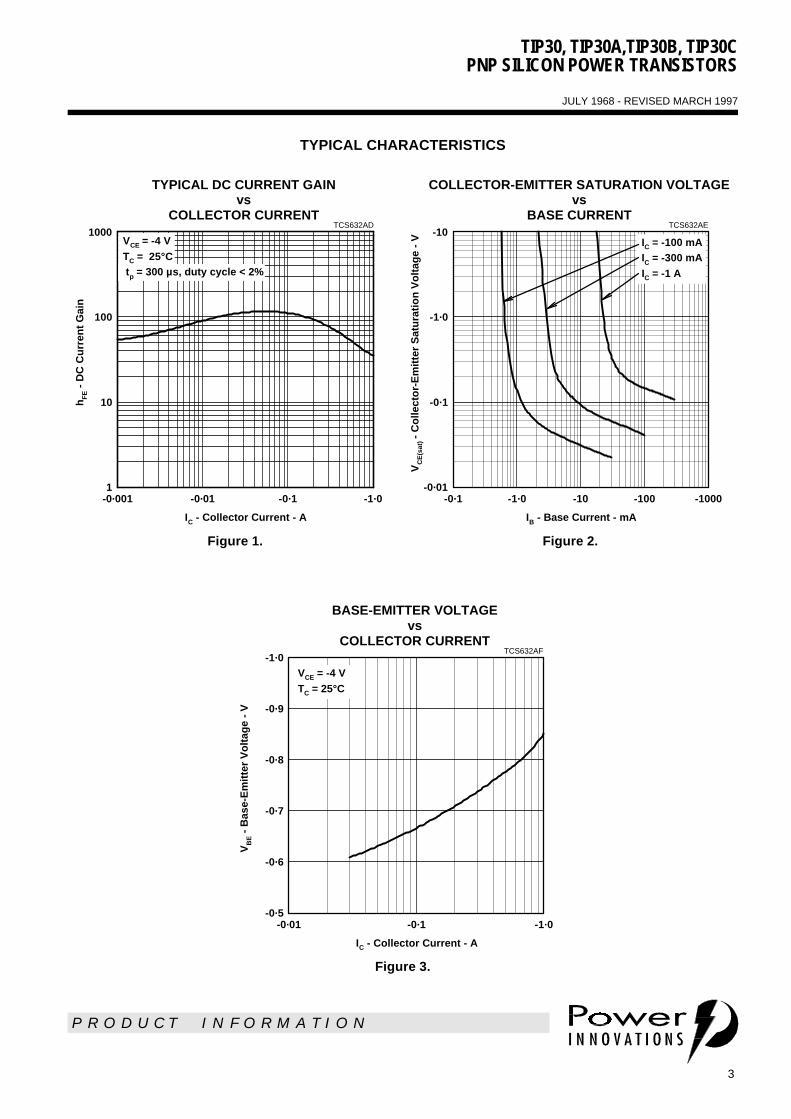
TYPICAL DC CURRENT GAINvs
COLLECTOR CURRENT
IC - Collector Current - A
-0·001 -0·01 -0·1 -1·0
hF
E -
DC
Cu
rren
t G
ain
1
10
100
1000TCS632AD
VCE = -4 VTC = 25°C tp = 300 µs, duty cycle < 2%
COLLECTOR-EMITTER SATURATION VOLTAGEvs
BASE CURRENT
IB - Base Current - mA
-0·1 -1·0 -10 -100 -1000
VC
E(s
at) -
Co
llect
or-
Em
itte
r S
atu
rati
on
Vo
ltag
e -
V
-0·01
-0·1
-1·0
-10TCS632AE
IC = -100 mAIC = -300 mAIC = -1 A
BASE-EMITTER VOLTAGEvs
COLLECTOR CURRENT
IC - Collector Current - A
-0·01 -0·1 -1·0
VB
E -
Bas
e-E
mit
ter
Vo
ltag
e -
V
-0·5
-0·6
-0·7
-0·8
-0·9
-1·0TCS632AF
VCE = -4 VTC = 25°C
TIP30, TIP30A,TIP30B, TIP30CPNP SILICON POWER TRANSISTORS
4
JULY 1968 - REVISED MARCH 1997
P R O D U C T I N F O R M A T I O N
MAXIMUM SAFE OPERATING REGIONS
Figure 4.
THERMAL INFORMATION
Figure 5.
MAXIMUM FORWARD-BIASSAFE OPERATING AREA
VCE - Collector-Emitter Voltage - V
-1·0 -10 -100 -1000
I C -
Co
llect
or
Cu
rren
t -
A
-0·01
-0·1
-1·0
-10
-100SAS632AB
TIP30TIP30ATIP30BTIP30C
tp = 300 µs, d = 0.1 = 10%tp = 1 ms, d = 0.1 = 10%tp = 10 ms, d = 0.1 = 10%DC Operation
MAXIMUM POWER DISSIPATIONvs
CASE TEMPERATURE
TC - Case Temperature - °C
0 25 50 75 100 125 150
Pto
t - M
axim
um
Po
wer
Dis
sip
atio
n -
W
0
10
20
30
40TIS631AB
TL071, TL071A, TL071B, TL072TL072A, TL072B, TL074, TL074A, TL074B
LOW-NOISE JFET-INPUT OPERATIONAL AMPLIFIERS
SLOS080D – SEPTEMBER 1978 – REVISED AUGUST 1996
1POST OFFICE BOX 655303 • DALLAS, TEXAS 75265
Low Power Consumption
Wide Common-Mode and DifferentialVoltage Ranges
Low Input Bias and Offset Currents
Output Short-Circuit Protection
Low Total Harmonic Distortion0.003% Typ
Low NoiseVn = 18 nV/√Hz Typ at f = 1 kHz
High Input Impedanc e . . . JFET Input Stage
Internal Frequency Compensation
Latch-Up-Free Operation
High Slew Rat e . . . 13 V/µs Typ
Common-Mode Input Voltage RangeIncludes V CC+
description
The JFET-input operational amplifiers in the TL07_ series are designed as low-noise versions of the TL08_series amplifiers with low input bias and offset currents and fast slew rate. The low harmonic distortion and lownoise make the TL07_ series ideally suited for high-fidelity and audio preamplifier applications. Each amplifierfeatures JFET inputs (for high input impedance) coupled with bipolar output stages integrated on a singlemonolithic chip.
The C-suffix devices are characterized for operation from 0°C to 70°C. The I-suffix devices are characterizedfor operation from –40°C to 85°C. The M-suffix devices are characterized for operation over the full militarytemperature range of –55°C to 125°C.
AVAILABLE OPTIONS
PACKAGE
TAVIOmaxAT 25°C
SMALLOUTLINE
(D)†
CHIPCARRIER
(FK)
CERAMICDIP(J)
CERAMICDIP(JG)
PLASTICDIP(N)
PLASTICDIP(P)
TSSOPPACKAGE
(PW)
FLATPACKAGE
(W)
10 mV TL071CD TL071CP TL071CPWLE10 mV6 mV
TL071CDTL071ACD — — — —
TL071CPTL071ACP
TL071CPWLE— —
3 mV TL071BCD TL071BCP —
0°C to10 mV TL072CD TL072CP TL072CPWLE
0°C to70°C
10 mV6 mV
TL072CDTL072ACD — — — —
TL072CPTL072ACP
TL072CPWLE— —
70°C3 mV TL072BCD TL072BCP —
10 mV TL074CD TL074CN TL074CPWLE10 mV6 mV
TL074CDTL074ACD — — —
TL074CNTL074ACN —
TL074CPWLE— —
3 mV TL074BCD TL074BCN —
40°C toTL071ID — TL071IP
–40°C to85°C
6 mVTL071IDTL072ID — — — —
TL071IPTL072IP — —
85°CTL074ID TL074IN —
55°C to6 mV TL071MFK — TL071MJG — — —
–55°C to125°C 6 mV — TL072MFK — TL072MJG — TL072MP — —125 C
9 mV TL074MFK TL074MJ — TL074MN — TL074MW
† The D package is available taped and reeled. Add the suffix R to the device type (e.g., TL071CDR). The PW package is only available left-endedtaped and reeled (e.g., TL072CPWLE).
Please be aware that an important notice concerning availability, standard warranty, and use in critical applications ofTexas Instruments semiconductor products and disclaimers thereto appears at the end of this data sheet.
Copyright 1996, Texas Instruments IncorporatedPRODUCTION DATA information is current as of publication date.Products conform to specifications per the terms of Texas Instrumentsstandard warranty. Production processing does not necessarily includetesting of all parameters.
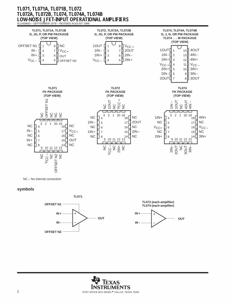
TL071, TL071A, TL071B, TL072TL072A, TL072B, TL074, TL074A, TL074BLOW-NOISE JFET-INPUT OPERATIONAL AMPLIFIERS
SLOS080D – SEPTEMBER 1978 – REVISED AUGUST 1996
2 POST OFFICE BOX 655303 • DALLAS, TEXAS 75265
NC2OUTNC2IN–NC
1IN+NC
VCC+NC
2IN+
NCVCC+NCOUTNC
3 2 1 20 19
9 10 11 12 13
4
5
6
7
8
18
17
16
15
14
NC1IN–
NC1IN+
NC
(TOP VIEW)
NC
1OU
TN
C
NC
NC
NC
NC
2IN
+
CC
–V
CC
+V
1
2
3
4
5
6
7
14
13
12
11
10
9
8
1OUT1IN–1IN+
VCC +2IN+2IN–
2OUT
4OUT4IN–4IN+VCC –3IN+3IN–3OUT
TL074, TL074A, TL074BD, J, N, OR PW PACKAGE
TL074 . . . W PACKAGE(TOP VIEW)
NC – No internal connection
3 2 1 20 19
9 10 11 12 13
4
5
6
7
8
18
17
16
15
14
NCIN–NCIN+NC
TL071FK PACKAGE(TOP VIEW)
NC
OF
FS
ET
N1
NC
NC
NC
NC
NC
OF
FS
ET
N2
NC
CC
–V
TL072FK PACKAGE
3 2 1 20 19
9 10 11 12 13
4
5
6
7
8
18
17
16
15
14
4IN+NCVCC –NC3IN+
TL074FK PACKAGE(TOP VIEW)
1IN
–1O
UT
NC
3IN
–4I
N –
2IN
–
NC
3OU
T4O
UT
2OU
T
1
2
3
4
8
7
6
5
OFFSET N1IN–IN+
VCC –
NCVCC+
OUT
OFFSET N2
TL071, TL071A, TL071BD, JG, P, OR PW PACKAGE
(TOP VIEW)
1
2
3
4
8
7
6
5
1OUT1IN–1IN+
VCC –
VCC +2OUT2IN–2IN+
TL072, TL072A, TL072BD, JG, P, OR PW PACKAGE
(TOP VIEW)
symbols
+
–
+
–
IN+
IN–OUT
IN+
IN–OUT
TL072 (each amplifier)TL074 (each amplifier)
TL071
OFFSET N1
OFFSET N2
TL071, TL071A, TL071B, TL072TL072A, TL072B, TL074, TL074A, TL074B
LOW-NOISE JFET-INPUT OPERATIONAL AMPLIFIERS
SLOS080D – SEPTEMBER 1978 – REVISED AUGUST 1996
3POST OFFICE BOX 655303 • DALLAS, TEXAS 75265
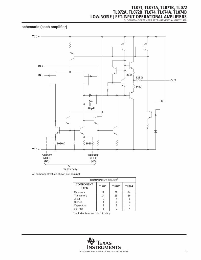
schematic (each amplifier)
C1
VCC+
IN +
VCC–
1080 Ω ÎÎÎ1080 Ω
IN –
TL071 Only
64 Ω128 Ω
64 Ω
All component values shown are nominal.
ÁÁÁÁÁÁÁÁÁÁÁÁÁÁÁ
OFFSETNULL(N1)
ÁÁÁÁÁÁÁÁÁ
OFFSETNULL(N2)
OUT
18 pF
COMPONENT COUNT†
COMPONENTTYPE TL071 TL072 TL074
Resistors 11 22 44ResistorsTransistors
1114
2228
4456
JFET 2 4 6Diodes 1 2 4Capacitors 1 2 4epi-FET 1 2 4
† Includes bias and trim circuitry
TL071, TL071A, TL071B, TL072TL072A, TL072B, TL074, TL074A, TL074BLOW-NOISE JFET-INPUT OPERATIONAL AMPLIFIERS
SLOS080D – SEPTEMBER 1978 – REVISED AUGUST 1996
4 POST OFFICE BOX 655303 • DALLAS, TEXAS 75265
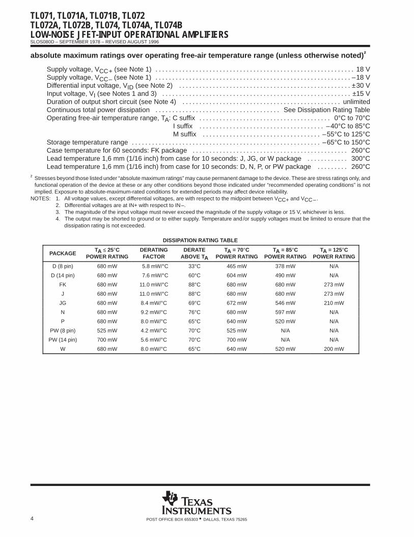
absolute maximum ratings over operating free-air temperature range (unless otherwise noted) †
Supply voltage, VCC+ (see Note 1) 18 V. . . . . . . . . . . . . . . . . . . . . . . . . . . . . . . . . . . . . . . . . . . . . . . . . . . . . . . . . . . Supply voltage, VCC– (see Note 1) –18 V. . . . . . . . . . . . . . . . . . . . . . . . . . . . . . . . . . . . . . . . . . . . . . . . . . . . . . . . . . Differential input voltage, VID (see Note 2) ±30 V. . . . . . . . . . . . . . . . . . . . . . . . . . . . . . . . . . . . . . . . . . . . . . . . . . . Input voltage, VI (see Notes 1 and 3) ±15 V. . . . . . . . . . . . . . . . . . . . . . . . . . . . . . . . . . . . . . . . . . . . . . . . . . . . . . . . Duration of output short circuit (see Note 4) unlimited. . . . . . . . . . . . . . . . . . . . . . . . . . . . . . . . . . . . . . . . . . . . . . . Continuous total power dissipation See Dissipation Rating Table. . . . . . . . . . . . . . . . . . . . . . . . . . . . . . . . . . . . . Operating free-air temperature range, TA: C suffix 0°C to 70°C. . . . . . . . . . . . . . . . . . . . . . . . . . . . . . . . . . . . . . .
I suffix –40°C to 85°C. . . . . . . . . . . . . . . . . . . . . . . . . . . . . . . . . . . . . M suffix –55°C to 125°C. . . . . . . . . . . . . . . . . . . . . . . . . . . . . . . . . . .
Storage temperature range –65°C to 150°C. . . . . . . . . . . . . . . . . . . . . . . . . . . . . . . . . . . . . . . . . . . . . . . . . . . . . . . . Case temperature for 60 seconds: FK package 260°C. . . . . . . . . . . . . . . . . . . . . . . . . . . . . . . . . . . . . . . . . . . . . . Lead temperature 1,6 mm (1/16 inch) from case for 10 seconds: J, JG, or W package 300°C. . . . . . . . . . . . Lead temperature 1,6 mm (1/16 inch) from case for 10 seconds: D, N, P, or PW package 260°C. . . . . . . . .
† Stresses beyond those listed under “absolute maximum ratings” may cause permanent damage to the device. These are stress ratings only, andfunctional operation of the device at these or any other conditions beyond those indicated under “recommended operating conditions” is notimplied. Exposure to absolute-maximum-rated conditions for extended periods may affect device reliability.
NOTES: 1. All voltage values, except differential voltages, are with respect to the midpoint between VCC+ and VCC–.2. Differential voltages are at IN+ with respect to IN–.3. The magnitude of the input voltage must never exceed the magnitude of the supply voltage or 15 V, whichever is less.4. The output may be shorted to ground or to either supply. Temperature and /or supply voltages must be limited to ensure that the
dissipation rating is not exceeded.
DISSIPATION RATING TABLE
PACKAGETA ≤ 25°C
POWER RATINGDERATINGFACTOR
DERATEABOVE TA
TA = 70°CPOWER RATING
TA = 85°CPOWER RATING
TA = 125°CPOWER RATING
D (8 pin) 680 mW 5.8 mW/°C 33°C 465 mW 378 mW N/A
D (14 pin) 680 mW 7.6 mW/°C 60°C 604 mW 490 mW N/A
FK 680 mW 11.0 mW/°C 88°C 680 mW 680 mW 273 mW
J 680 mW 11.0 mW/°C 88°C 680 mW 680 mW 273 mW
JG 680 mW 8.4 mW/°C 69°C 672 mW 546 mW 210 mW
N 680 mW 9.2 mW/°C 76°C 680 mW 597 mW N/A
P 680 mW 8.0 mW/°C 65°C 640 mW 520 mW N/A
PW (8 pin) 525 mW 4.2 mW/°C 70°C 525 mW N/A N/A
PW (14 pin) 700 mW 5.6 mW/°C 70°C 700 mW N/A N/A
W 680 mW 8.0 mW/°C 65°C 640 mW 520 mW 200 mW
TL071, TL071A, TL071B, TL072TL072A, TL072B, TL074, TL074A, TL074B
LOW
-NOISE JFET-INPUT O
PERATIONAL AM
PLIFIERSS
LOS
080D – S
EP
TE
MB
ER
1978 – RE
VIS
ED
AU
GU
ST
1996
PO
ST
OF
FIC
E B
OX
655303 DA
LLAS
, TE
XA
S 75265
•5
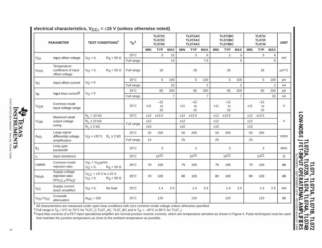
electrical characteristics, V CC± = ±15 V (unless otherwise noted)
† ‡
TL071C TL071AC TL071BC TL071I
PARAMETER TEST CONDITIONS† T ‡
TL071CTL072C
TL071ACTL072AC
TL071BCTL072BC
TL071ITL072I
UNITPARAMETER TEST CONDITIONS† TA‡TL074C TL074AC TL074BC TL074I UNIT
MIN TYP MAX MIN TYP MAX MIN TYP MAX MIN TYP MAX
VIO Input offset voltage VO = 0 RS = 50 Ω25°C 3 10 3 6 2 3 3 6
mVVIO Input offset voltage VO = 0, RS = 50 ΩFull range 13 7.5 5 8
mV
αVIO
Temperaturecoefficient of inputoffset voltage
VO = 0, RS = 50 Ω Full range 18 18 18 18 µV/°C
IIO Input offset current VO = 025°C 5 100 5 100 5 100 5 100 pA
IIO Input offset current VO = 0Full range 10 2 2 2 nA
IIB Input bias current§ VO = 025°C 65 200 65 200 65 200 65 200 pA
IIB Input bias current§ VO = 0Full range 7 7 7 20 nA
Common mode–12 –12 –12 –12
VICRCommon-modeinput voltage range
25°C ±1112to ±11
12to ±11
12to ±11
12to VICR in ut voltage range
15 15 15 15
Maximum peak RL = 10 kΩ 25°C ±12 ±13.5 ±12 ±13.5 ±12 ±13.5 ±12 ±13.5
VOM
Maximum eakoutput voltage RL ≥ 10 kΩ
Full range±12 ±12 ±12 ±12 V
swing RL ≥ 2 kΩFull range
±10 ±10 ±10 ±10
AVD
Large-signaldifferential voltage VO = ±10 V RL ≥ 2 kΩ
25°C 25 200 50 200 50 200 50 200V/mVAVD differential voltage
amplificationVO = ±10 V, RL ≥ 2 kΩ
Full range 15 25 25 25V/mV
B1Unity-gainbandwidth
25°C 3 3 3 3 MHz
ri Input resistance 25°C 1012 1012 1012 1012 Ω
CMRRCommon-mode VIC = VICRmin,
25°C 70 100 75 100 75 100 75 100 dBCMRR rejection ratio VO = 0, RS = 50 Ω25°C 70 100 75 100 75 100 75 100 dB
kSVR
Supply-voltagerejection ratio
VCC = ±9 V to ±15 V,25°C 70 100 80 100 80 100 80 100 dBkSVR rejection ratio
(∆VCC± /∆VIO) VO = 0, RS = 50 Ω 25°C 70 100 80 100 80 100 80 100 dB
ICCSupply current
VO = 0 No load 25°C 1 4 2 5 1 4 2 5 1 4 2 5 1 4 2 5 mAICCy
(each amplifier)VO = 0, No load 25°C 1.4 2.5 1.4 2.5 1.4 2.5 1.4 2.5 mA
VO1/VO2Crosstalkattenuation
AVD = 100 25°C 120 120 120 120 dB
† All characteristics are measured under open-loop conditions with zero common-mode voltage unless otherwise specified.‡ Full range is TA = 0°C to 70°C for TL07_C,TL07_AC, TL07_BC and is TA = –40°C to 85°C for TL07_I.§ Input bias currents of a FET-input operational amplifier are normal junction reverse currents, which are temperature sensitive as shown in Figure 4. Pulse techniques must be used
that maintain the junction temperature as close to the ambient temperature as possible.
TL071, TL071A, TL071B, TL072TL072A, TL072B, TL074, TL074A, TL074BLOW-NOISE JFET-INPUT OPERATIONAL AMPLIFIERS
SLOS080D – SEPTEMBER 1978 – REVISED AUGUST 1996
6 POST OFFICE BOX 655303 • DALLAS, TEXAS 75265
electrical characteristics, V CC± = ±15 V (unless otherwise noted)
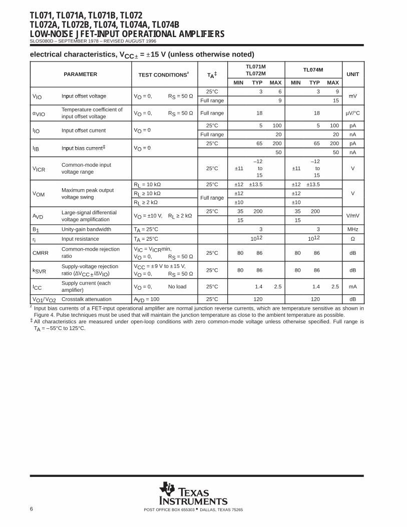
† ‡TL071M
TL074MPARAMETER TEST CONDITIONS† TA‡ TL072M
TL074MUNITA
MIN TYP MAX MIN TYP MAX
VIO Input offset voltage VO = 0 RS = 50 Ω25°C 3 6 3 9
mVVIO Input offset voltage VO = 0, RS = 50 ΩFull range 9 15
mV
αVIOTemperature coefficient ofinput offset voltage
VO = 0, RS = 50 Ω Full range 18 18 µV/°C
IIO Input offset current VO = 025°C 5 100 5 100 pA
IIO Input offset current VO = 0Full range 20 20 nA
IIB Input bias current‡ VO = 025°C 65 200 65 200 pA
IIB Input bias current‡ VO = 050 50 nA
VICRCommon-mode inputvoltage range
25°C ±11–12
to15
±11–12
to15
V
M i k t tRL = 10 kΩ 25°C ±12 ±13.5 ±12 ±13.5
VOMMaximum peak outputvoltage swing
RL ≥ 10 kΩFull range
±12 ±12 Vvoltage swing
RL ≥ 2 kΩFull range
±10 ±10
AVDLarge-signal differential
VO = ±10 V RL ≥ 2 kΩ25°C 35 200 35 200
V/mVAVDg g
voltage amplificationVO = ±10 V, RL ≥ 2 kΩ
15 15V/mV
B1 Unity-gain bandwidth TA = 25°C 3 3 MHz
ri Input resistance TA = 25°C 1012 1012 Ω
CMRRCommon-mode rejection VIC = VICRmin,
25°C 80 86 80 86 dBCMRR ratio VO = 0, RS = 50 Ω25°C 80 86 80 86 dB
kSVRSupply-voltage rejection VCC = ±9 V to ±15 V,
25°C 80 86 80 86 dBkSVR ratio (∆VCC± /∆VIO) VO = 0, RS = 50 Ω25°C 80 86 80 86 dB
ICCSupply current (eachamplifier)
VO = 0, No load 25°C 1.4 2.5 1.4 2.5 mA
VO1/VO2 Crosstalk attenuation AVD = 100 25°C 120 120 dB
† Input bias currents of a FET-input operational amplifier are normal junction reverse currents, which are temperature sensitive as shown inFigure 4. Pulse techniques must be used that will maintain the junction temperature as close to the ambient temperature as possible.
‡ All characteristics are measured under open-loop conditions with zero common-mode voltage unless otherwise specified. Full range isTA = –55°C to 125°C.
TL071, TL071A, TL071B, TL072TL072A, TL072B, TL074, TL074A, TL074B
LOW-NOISE JFET-INPUT OPERATIONAL AMPLIFIERS
SLOS080D – SEPTEMBER 1978 – REVISED AUGUST 1996
7POST OFFICE BOX 655303 • DALLAS, TEXAS 75265
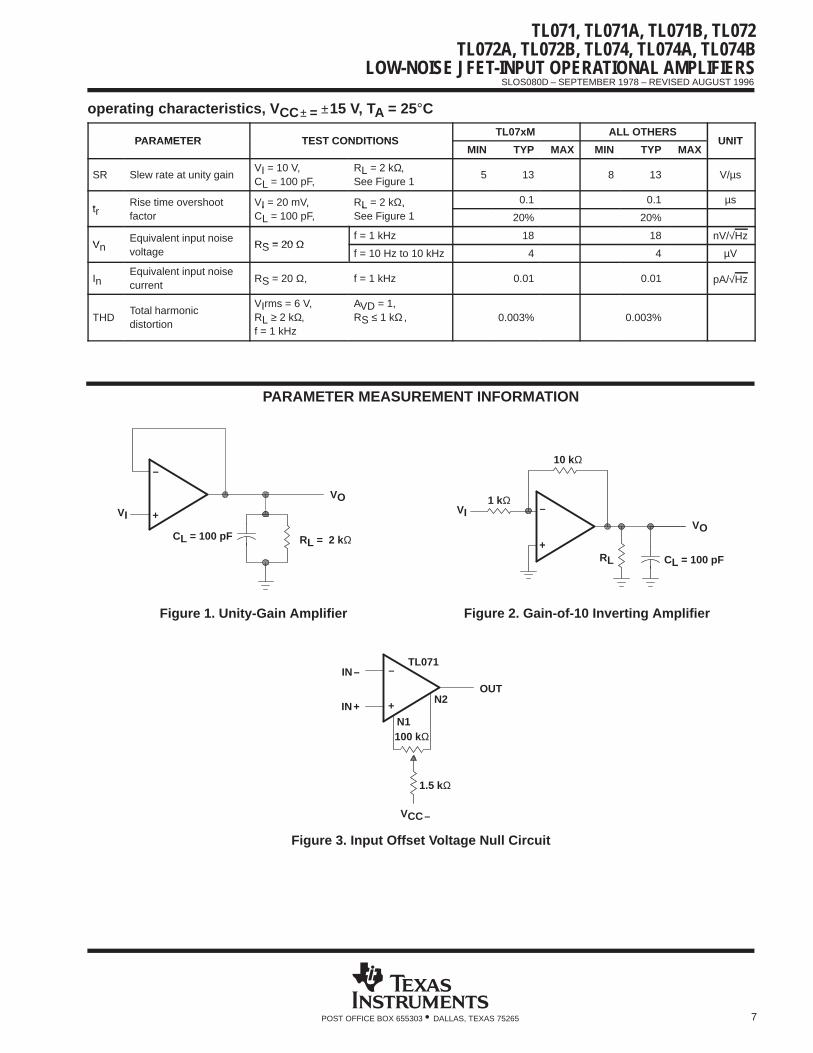
operating characteristics, V CC± = ±15 V, TA = 25°C
PARAMETER TEST CONDITIONSTL07xM ALL OTHERS
UNITPARAMETER TEST CONDITIONSMIN TYP MAX MIN TYP MAX
UNIT
SR Slew rate at unity gainVI = 10 V,CL = 100 pF,
RL = 2 kΩ,See Figure 1
5 13 8 13 V/µs
tRise time overshoot VI = 20 mV, RL = 2 kΩ, 0.1 0.1 µs
tr factorI ,
CL = 100 pF,L ,
See Figure 1 20% 20%
VEquivalent input noise
RS = 20 Ωf = 1 kHz 18 18 nV/√Hz
Vnq
voltageRS = 20 Ω
f = 10 Hz to 10 kHz 4 4 µV
InEquivalent input noisecurrent
RS = 20 Ω, f = 1 kHz 0.01 0.01 pA/√Hz
THDTotal harmonicdistortion
VIrms = 6 V,RL ≥ 2 kΩ,f = 1 kHz
AVD = 1,RS ≤ 1 kΩ , 0.003% 0.003%
PARAMETER MEASUREMENT INFORMATION
Figure 1. Unity-Gain Amplifier
VI
+
–
CL = 100 pF RL = 2 kΩ
VO
Figure 2. Gain-of-10 Inverting Amplifier
VI+
–
10 kΩ
1 kΩ
RL CL = 100 pF
VO
N1100 kΩ
+
– TL071
N2
1.5 kΩ
VCC–
OUT
IN–
IN+
Figure 3. Input Offset Voltage Null Circuit
TL071, TL071A, TL071B, TL072TL072A, TL072B, TL074, TL074A, TL074BLOW-NOISE JFET-INPUT OPERATIONAL AMPLIFIERS
SLOS080D – SEPTEMBER 1978 – REVISED AUGUST 1996
8 POST OFFICE BOX 655303 • DALLAS, TEXAS 75265
TYPICAL CHARACTERISTICS
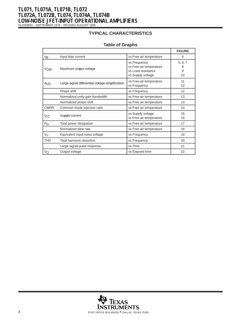
Table of GraphsFIGURE
IIB Input bias current vs Free-air temperature 4
vs Frequency 5, 6, 7
VOM Maximum output voltage
vs Frequencyvs Free-air temperature
5, 6, 78
VOM Maximum output voltagevs Load resistance 9vs Supply voltage 10
AVD Large signal differential voltage amplificationvs Free-air temperature 11
AVD Large-signal differential voltage amplificationvs Frequency 12
Phase shift vs Frequency 12
Normalized unity-gain bandwidth vs Free-air temperature 13
Normalized phase shift vs Free-air temperature 13
CMRR Common-mode rejection ratio vs Free-air temperature 14
ICC Supply currentvs Supply voltage 15
ICC Supply currenty g
vs Free-air temperature 16
PD Total power dissipation vs Free-air temperature 17
Normalized slew rate vs Free-air temperature 18
Vn Equivalent input noise voltage vs Frequency 19
THD Total harmonic distortion vs Frequency 20
Large-signal pulse response vs Time 21
VO Output voltage vs Elapsed time 22
TL071, TL071A, TL071B, TL072TL072A, TL072B, TL074, TL074A, TL074B
LOW-NOISE JFET-INPUT OPERATIONAL AMPLIFIERS
SLOS080D – SEPTEMBER 1978 – REVISED AUGUST 1996
9POST OFFICE BOX 655303 • DALLAS, TEXAS 75265
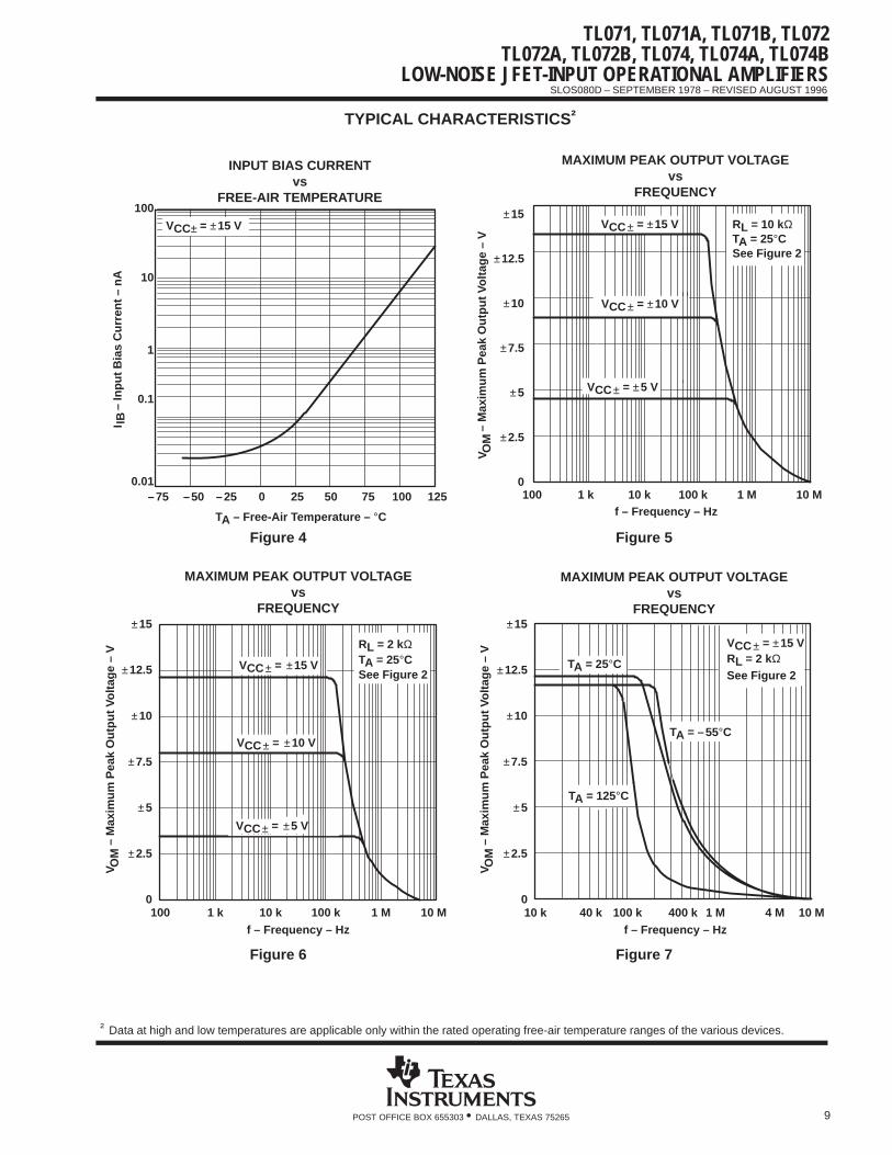
TYPICAL CHARACTERISTICS †
Figure 4
IIB–
Inpu
t Bia
s C
urre
nt –
nA
TA – Free-Air Temperature – °C
INPUT BIAS CURRENTvs
FREE-AIR TEMPERATURE
IBI
10
1
0.1
0.01
100
–75 –50 –25 0 25 50 75 100 125
VCC± = ±15 V
Figure 5
VCC± = ±5 V
VCC± = ±15 V RL = 10 kΩTA = 25°CSee Figure 2
±15
±12.5
±10
±7.5
±5
±2.5
0V
OM
– M
axim
um P
eak
Out
put V
olta
ge –
V
f – Frequency – Hz100 1 k 10 k 100 k 1 M 10 M
MAXIMUM PEAK OUTPUT VOLTAGEvs
FREQUENCY
ÁÁÁÁÁÁV
OM
ÎÎÎÎÎÎÎÎÎÎ
VCC± = ±10 V
Figure 6
10 M1 M100 k10 k1 k100f – Frequency – Hz
VO
M –
Max
imum
Pea
k O
utpu
t Vol
tage
– V
0
±2.5
±5
±7.5
±10
±12.5
±15
See Figure 2TA = 25°CRL = 2 kΩ
VCC± = ±10 V
VCC± = ±5 V
MAXIMUM PEAK OUTPUT VOLTAGEvs
FREQUENCY
ÁÁÁÁÁÁ
V OM
ÎÎÎÎÎÎÎÎÎÎ
VCC± = ±15 V
Figure 7
0
±2.5
±5
±7.5
±10
±12.5
±15
10 k 40 k 100 k 400 k 1 M 4 M 10 Mf – Frequency – Hz
MAXIMUM PEAK OUTPUT VOLTAGEvs
FREQUENCY
VO
M –
Max
imum
Pea
k O
utpu
t Vol
tage
– V
ÁÁÁÁÁÁÁÁÁ
V OM
VCC± = ±15 VRL = 2 kΩSee Figure 2
ÎÎÎÎÎÎÎÎÎÎ
TA = –55°C
ÎÎÎÎÎÎÎÎ
TA = 25°C
TA = 125°C
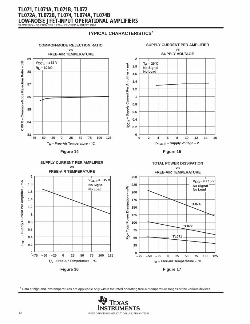
† Data at high and low temperatures are applicable only within the rated operating free-air temperature ranges of the various devices.
TL071, TL071A, TL071B, TL072TL072A, TL072B, TL074, TL074A, TL074BLOW-NOISE JFET-INPUT OPERATIONAL AMPLIFIERS
SLOS080D – SEPTEMBER 1978 – REVISED AUGUST 1996
10 POST OFFICE BOX 655303 • DALLAS, TEXAS 75265
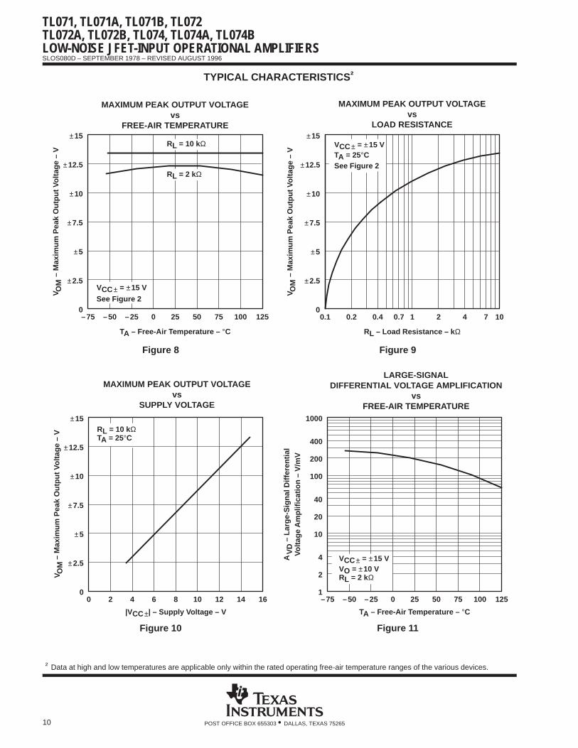
TYPICAL CHARACTERISTICS †
Figure 8
–750
VO
M –
Max
imum
Pea
k O
utpu
t Vol
tage
– V
TA – Free-Air Temperature – °C
125
±15
–50 –25 0 25 50 75 100
±2.5
±5
±7.5
±10
±12.5
RL = 10 kΩ
VCC± = ±15 V
See Figure 2
MAXIMUM PEAK OUTPUT VOLTAGEvs
FREE-AIR TEMPERATURE
ÁÁÁÁ
V OM
ÎÎÎÎÎÎÎÎ
RL = 2 kΩ
Figure 9
0.10
RL – Load Resistance – k Ω
10
±15
±2.5
±5
±7.5
±10
±12.5
VCC± = ±15 VTA = 25°CSee Figure 2
0.2 0.4 0.7 1 2 4 7
MAXIMUM PEAK OUTPUT VOLTAGEvs
LOAD RESISTANCE
VO
M –
Max
imum
Pea
k O
utpu
t Vol
tage
– V
ÁÁÁÁ
V OM
Figure 10
00
VO
M –
Max
imum
Pea
k O
utpu
t Vol
tage
– V
|VCC±| – Supply Voltage – V
16
±15
2 4 6 8 10 12 14
±2.5
±5
±7.5
±10
±12.5
RL = 10 kΩTA = 25°C
MAXIMUM PEAK OUTPUT VOLTAGEvs
SUPPLY VOLTAGE
ÁÁÁÁÁÁ
V OM
Figure 11
–751
Volta
ge A
mpl
ifica
tion
– V
/mV
TA – Free-Air Temperature – °C
125
1000
–50 –25 0 25 50 75 100
2
4
10
20
40
100
200
400
VCC± = ±15 VVO = ±10 VRL = 2 kΩ
LARGE-SIGNALDIFFERENTIAL VOLTAGE AMPLIFICATION
vsFREE-AIR TEMPERATURE
AV
D –
Lar
ge-S
igna
l Diff
eren
tial
AV
D
† Data at high and low temperatures are applicable only within the rated operating free-air temperature ranges of the various devices.
TL071, TL071A, TL071B, TL072TL072A, TL072B, TL074, TL074A, TL074B
LOW-NOISE JFET-INPUT OPERATIONAL AMPLIFIERS
SLOS080D – SEPTEMBER 1978 – REVISED AUGUST 1996
11POST OFFICE BOX 655303 • DALLAS, TEXAS 75265
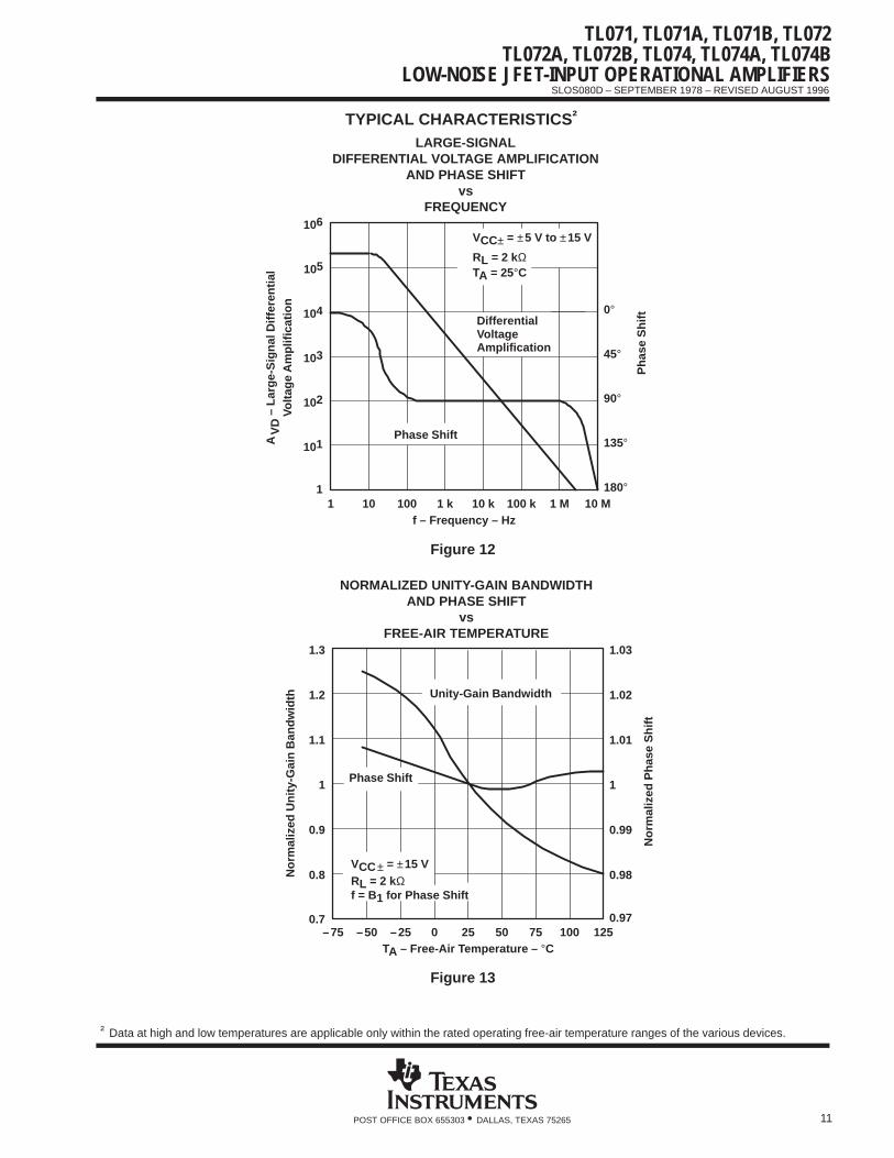
TYPICAL CHARACTERISTICS †
0°
45°
180°
135°
90°
11
f – Frequency – Hz10 M
106
10 100 1 k 10 k 100 k 1 M
101
102
103
104
105
DifferentialVoltageAmplification
VCC± = ±5 V to ±15 V
RL = 2 kΩTA = 25°C
Phase Shift
LARGE-SIGNALDIFFERENTIAL VOLTAGE AMPLIFICATION
AND PHASE SHIFTvs
FREQUENCY
Volta
ge A
mpl
ifica
tion
AV
D –
Lar
ge-S
igna
l Diff
eren
tial
AV
D
Pha
se S
hift
Figure 12
1.02
1.01
1
0.99
0.98
1.03
0.97–75
0.7
Nor
mal
ized
Uni
ty-G
ain
Ban
dwid
th
TA – Free-Air Temperature – °C125
1.3
–50 –25 0 25 50 75 100
0.8
0.9
1
1.1
1.2 Unity-Gain Bandwidth
VCC± = ±15 VRL = 2 kΩf = B1 for Phase Shift
NORMALIZED UNITY-GAIN BANDWIDTHAND PHASE SHIFT
vsFREE-AIR TEMPERATURE
Nor
mal
ized
Pha
se S
hift
Phase Shift
Figure 13
† Data at high and low temperatures are applicable only within the rated operating free-air temperature ranges of the various devices.
TL071, TL071A, TL071B, TL072TL072A, TL072B, TL074, TL074A, TL074BLOW-NOISE JFET-INPUT OPERATIONAL AMPLIFIERS
SLOS080D – SEPTEMBER 1978 – REVISED AUGUST 1996
12 POST OFFICE BOX 655303 • DALLAS, TEXAS 75265
TYPICAL CHARACTERISTICS †
Figure 14
–7583
CM
RR
– C
omm
on-M
ode
Rej
ectio
n R
atio
– d
B
TA – Free-Air Temperature – °C
125
89
–50 –25 0 25 50 75 100
84
85
86
87
88
VCC± = ±15 V
RL = 10 kΩ
COMMON-MODE REJECTION RATIOvs
FREE-AIR TEMPERATURE
Figure 15
00
|VCC±| – Supply Voltage – V
16
2
2 4 6 8 10 12 14
0.2
0.4
0.6
0.8
1
1.2
1.4
1.6
1.8TA = 25°CNo SignalNo Load
SUPPLY CURRENT PER AMPLIFIERvs
SUPPLY VOLTAGE
ICC
– S
uppl
y C
urre
nt P
er A
mpl
ifier
– m
AÁÁÁÁ
CC
±I
Figure 16
–750
TA – Free-Air Temperature – °C
125
2
–50 –25 0 25 50 75 100
0.2
0.4
0.6
0.8
1
1.2
1.4
1.6
1.8VCC± = ±15 VNo SignalNo Load
SUPPLY CURRENT PER AMPLIFIERvs
FREE-AIR TEMPERATURE
ICC
– S
uppl
y C
urre
nt P
er A
mpl
ifier
– m
A
ÁÁÁÁÁÁÁÁÁ
CC
±I
Figure 17
–750
TA – Free-Air Temperature – °C125
250
–50 –25 0 25 50 75 100
25
50
75
100
125
150
175
200
225VCC± = ±15 VNo SignalNo Load
TL074
TL071
TOTAL POWER DISSIPATIONvs
FREE-AIR TEMPERATURE
ÎÎÎÎÎÎÎÎ
TL072
PD
– T
otal
Pow
er D
issi
patio
n –
mW
PD
† Data at high and low temperatures are applicable only within the rated operating free-air temperature ranges of the various devices.
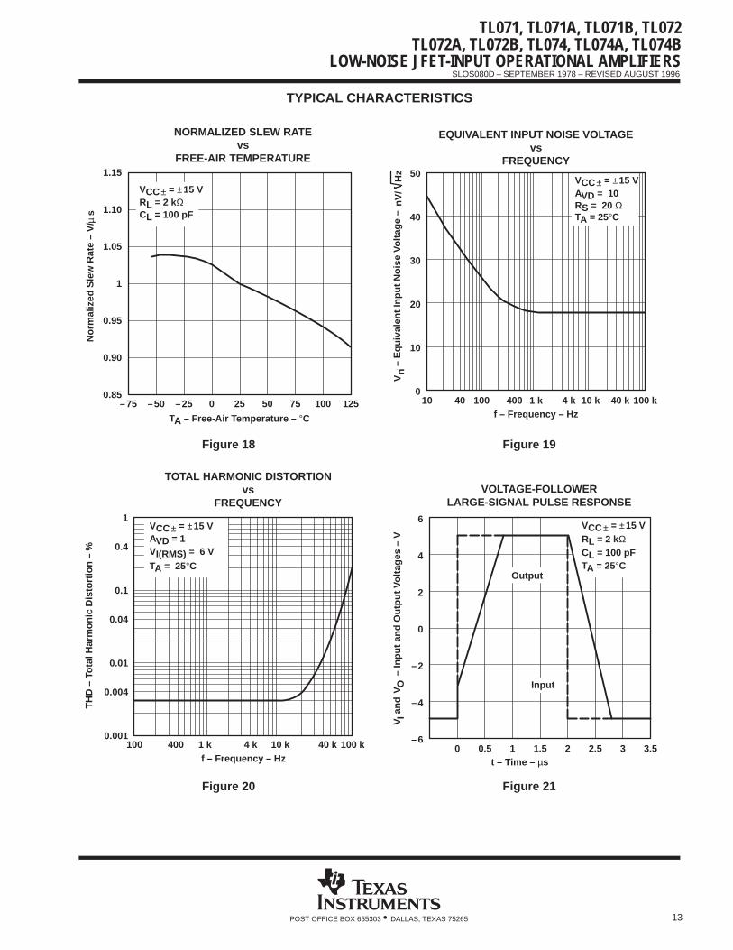
TL071, TL071A, TL071B, TL072TL072A, TL072B, TL074, TL074A, TL074B
LOW-NOISE JFET-INPUT OPERATIONAL AMPLIFIERS
SLOS080D – SEPTEMBER 1978 – REVISED AUGUST 1996
13POST OFFICE BOX 655303 • DALLAS, TEXAS 75265
TYPICAL CHARACTERISTICS
Figure 18
–750.85
TA – Free-Air Temperature – °C125
1.15
–50 –25 0 25 50 75 100
0.90
0.95
1
1.05
1.10
NORMALIZED SLEW RATEvs
FREE-AIR TEMPERATURE
VCC± = ±15 VRL = 2 kΩCL = 100 pFs
µN
orm
aliz
ed S
lew
Rat
e –
V/
Figure 19
100
Vn
– E
quiv
alen
t Inp
ut N
oise
Vol
tage
– n
V/H
z
f – Frequency – Hz100 k
50
10
20
30
40
VCC± = ±15 VAVD = 10RS = 20 ΩTA = 25°C
40 100 400 1 k 4 k 10 k 40 k
EQUIVALENT INPUT NOISE VOLTAGEvs
FREQUENCYÁÁÁÁÁÁÁÁÁÁÁÁ
nV/
Hz
Vn
Figure 20
0.001
TH
D –
Tot
al H
arm
onic
Dis
tort
ion
– %
1
40 k10 k4 k1 k400 100 kf – Frequency – Hz
100
0.004
0.01
0.04
0.1
0.4
TOTAL HARMONIC DISTORTIONvs
FREQUENCY
VCC± = ±15 VAVD = 1VI(RMS) = 6 V
TA = 25°C
Figure 21
–6
t – Time – µs3.5
6
0 0.5 1 1.5 2 2.5 3
–4
–2
0
2
4
Output
ÎÎÎÎÎÎ
Input
VCC± = ±15 VRL = 2 kΩ
TA = 25°C
VOLTAGE-FOLLOWERLARGE-SIGNAL PULSE RESPONSE
CL = 100 pF
ÁÁÁÁV
O
ÁÁÁÁ
VI
– In
put a
nd O
utpu
t Vol
tage
s –
Van
d
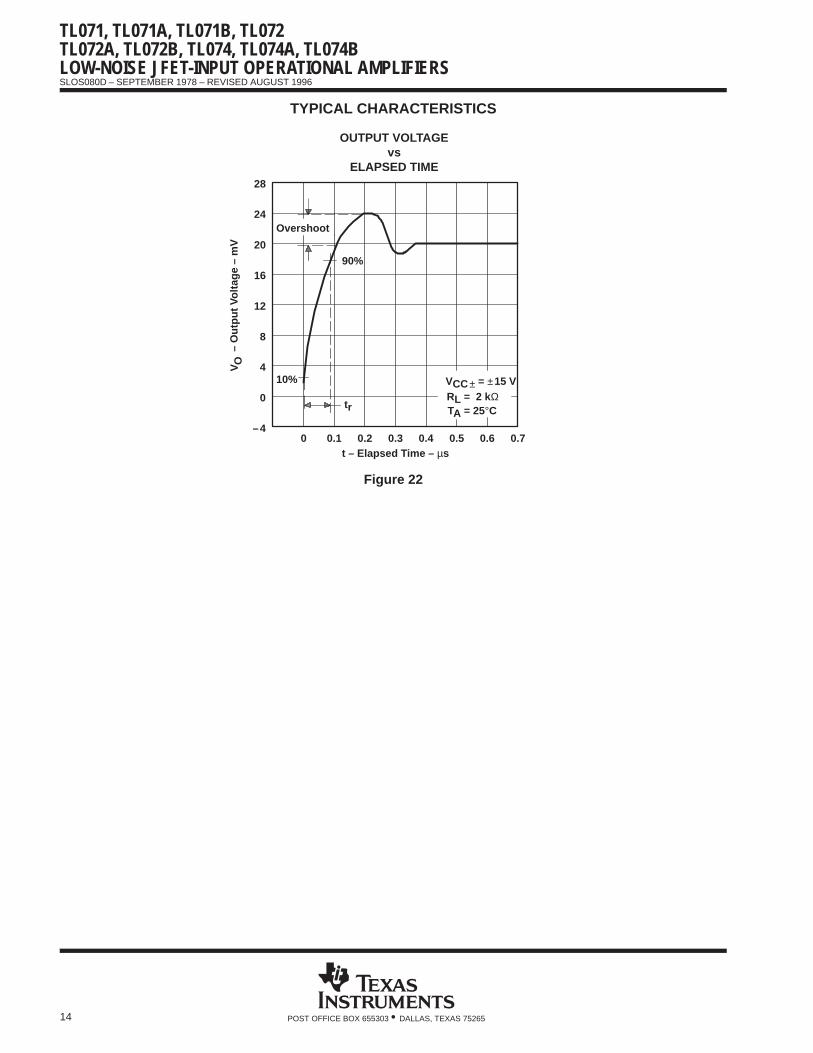
TL071, TL071A, TL071B, TL072TL072A, TL072B, TL074, TL074A, TL074BLOW-NOISE JFET-INPUT OPERATIONAL AMPLIFIERS
SLOS080D – SEPTEMBER 1978 – REVISED AUGUST 1996
14 POST OFFICE BOX 655303 • DALLAS, TEXAS 75265
TYPICAL CHARACTERISTICS
10%
–4
VO
– O
utpu
t Vol
tage
– m
V
t – Elapsed Time – µs0.7
28
0 0.1 0.2 0.3 0.4 0.5 0.6
0
4
8
12
16
20
24
VCC± = ±15 VRL = 2 kΩTA = 25°Ctr
Overshoot
90%
OUTPUT VOLTAGEvs
ELAPSED TIME
ÁÁÁÁÁÁ
VO
Figure 22
DeviceOperating
Temperature Range Package
SEMICONDUCTORTECHNICAL DATA
BALANCEDMODULATORS/DEMODULATORS
ORDERING INFORMATION
MC1496D
MC1496PTA = 0°C to +70°C
SO–14
Plastic DIP
PIN CONNECTIONS
Order this document by MC1496/D
D SUFFIXPLASTIC PACKAGE
CASE 751A(SO–14)
P SUFFIXPLASTIC PACKAGE
CASE 646
Signal Input 1
2
3
4
5
6
7
10
11
14
13
12
9
N/C
Output
Bias
Signal Input
Gain Adjust
Gain Adjust
Input Carrier8
VEE
N/C
Output
N/C
Carrier Input
N/C
14
1
14
1
MC1496BP Plastic DIPTA = –40°C to +125°C
1MOTOROLA ANALOG IC DEVICE DATA
These devices were designed for use where the output voltage is aproduct of an input voltage (signal) and a switching function (carrier). Typicalapplications include suppressed carrier and amplitude modulation,synchronous detection, FM detection, phase detection, and chopperapplications. See Motorola Application Note AN531 for additional designinformation.
• Excellent Carrier Suppression –65 dB typ @ 0.5 MHzExcellent Carrier Suppression –50 dB typ @ 10 MHz
• Adjustable Gain and Signal Handling
• Balanced Inputs and Outputs
• High Common Mode Rejection –85 dB typical
This device contains 8 active transistors.
Figure 1. SuppressedCarrier Output
Waveform
Figure 2. SuppressedCarrier Spectrum
Figure 3. AmplitudeModulation Output
Waveform
Figure 4. Amplitude–Modulation Spectrum
IC = 500 kHz, IS = 1.0 kHz
IC = 500 kHzIS = 1.0 kHz
60
40
20
0
Log
Scal
e Id
499 kHz 500 kHz 501 kHz
IC = 500 kHzIS = 1.0 kHz
IC = 500 kHzIS = 1.0 kHz
499 kHz 500 kHz 501 kHz
Line
ar S
cale
10
8.0
6.0
4.0
2.0
0
Motorola, Inc. 1996 Rev 4
MC1496, B
2 MOTOROLA ANALOG IC DEVICE DATA
MAXIMUM RATINGS (TA = 25°C, unless otherwise noted.)
Rating Symbol Value Unit
Applied Voltage(V6 – V8, V10 – V1, V12 – V8, V12 – V10, V8 – V4,V8 – V1, V10 – V4, V6 – V10, V2 – V5, V3 – V5)
∆V 30 Vdc
Differential Input Signal V8 – V10V4 – V1
+5.0±(5+ I5Re)
Vdc
Maximum Bias Current I5 10 mA
Thermal Resistance, Junction–to–AirPlastic Dual In–Line Package
RθJA 100 °C/W
Operating Temperature Range TA 0 to +70 °C
Storage Temperature Range Tstg –65 to +150 °C
NOTE: ESD data available upon request.
ELECTRICAL CHARACTERISTICS (VCC = 12 Vdc, VEE = –8.0 Vdc, I5 = 1.0 mAdc, RL = 3.9 kΩ, Re = 1.0 kΩ, TA = Tlow to Thigh,all input and output characteristics are single–ended, unless otherwise noted.)
Characteristic Fig. Note Symbol Min Typ Max Unit
Carrier FeedthroughVC = 60 mVrms sine wave and
offset adjusted to zeroVC = 300 mVpp square wave:
offset adjusted to zerooffset not adjusted
fC = 1.0 kHzfC = 10 MHz
fC = 1.0 kHzfC = 1.0 kHz
5 1 VCFT––
––
40140
0.0420
––
0.4200
µVrms
mVrms
Carrier SuppressionfS = 10 kHz, 300 mVrms
fC = 500 kHz, 60 mVrms sine wavefC = 10 MHz, 60 mVrms sine wave
5 2 VCS
40–
6550
––
dB
k
Transadmittance Bandwidth (Magnitude) (RL = 50 Ω)Carrier Input Port, VC = 60 mVrms sine wave
fS = 1.0 kHz, 300 mVrms sine waveSignal Input Port, VS = 300 mVrms sine wave|VC| = 0.5 Vdc
8 8 BW3dB–
–
300
80
–
–
MHz
Signal Gain (VS = 100 mVrms, f = 1.0 kHz; |VC|= 0.5 Vdc) 10 3 AVS 2.5 3.5 – V/V
Single–Ended Input Impedance, Signal Port, f = 5.0 MHzParallel Input ResistanceParallel Input Capacitance
6 –ripcip
––
2002.0
––
kΩpF
Single–Ended Output Impedance, f = 10 MHzParallel Output ResistanceParallel Output Capacitance
6 –ropcoo
––
405.0
––
kΩpF
Input Bias Current 7 –IbS 12 30
µA
IbSI1 I4
2; IbC
I8 I102
IbSIbC
––
1212
3030
Input Offset CurrentIioS = I1–I4; IioC = I8–I10
7 – IioSIioC
––
0.70.7
7.07.0
µA
Average Temperature Coefficient of Input Offset Current(TA = –55°C to +125°C)
7 – TCIio – 2.0 – nA/°C
Output Offset Current (I6–I9) 7 – Ioo – 14 80 µA
Average Temperature Coefficient of Output Offset Current(TA = –55°C to +125°C)
7 – TCIoo – 90 – nA/°C
Common–Mode Input Swing, Signal Port, fS = 1.0 kHz 9 4 CMV – 5.0 – Vpp
Common–Mode Gain, Signal Port, fS = 1.0 kHz, |VC|= 0.5 Vdc 9 – ACM – –85 – dB
Common–Mode Quiescent Output Voltage (Pin 6 or Pin 9) 10 – Vout – 8.0 – Vpp
Differential Output Voltage Swing Capability 10 – Vout – 8.0 – Vpp
Power Supply Current I6 +I12Power Supply Current I14
7 6 ICCIEE
––
2.03.0
4.05.0
mAdc
DC Power Dissipation 7 5 PD – 33 – mW
MC1496, B
3MOTOROLA ANALOG IC DEVICE DATA
GENERAL OPERATING INFORMATION
Carrier FeedthroughCarrier feedthrough is defined as the output voltage at
carrier frequency with only the carrier applied (signalvoltage = 0).
Carrier null is achieved by balancing the currents in thedifferential amplifier by means of a bias trim potentiometer(R1 of Figure 5).
Carrier SuppressionCarrier suppression is defined as the ratio of each
sideband output to carrier output for the carrier and signalvoltage levels specified.
Carrier suppression is very dependent on carrier inputlevel, as shown in Figure 22. A low value of the carrier doesnot fully switch the upper switching devices, and results inlower signal gain, hence lower carrier suppression. A higherthan optimum carrier level results in unnecessary device andcircuit carrier feedthrough, which again degenerates thesuppression figure. The MC1496 has been characterizedwith a 60 mVrms sinewave carrier input signal. This levelprovides optimum carrier suppression at carrier frequenciesin the vicinity of 500 kHz, and is generally recommended forbalanced modulator applications.
Carrier feedthrough is independent of signal level, VS.Thus carrier suppression can be maximized by operatingwith large signal levels. However, a linear operating modemust be maintained in the signal–input transistor pair – orharmonics of the modulating signal will be generated andappear in the device output as spurious sidebands of thesuppressed carrier. This requirement places an upper limit oninput–signal amplitude (see Figure 20). Note also that anoptimum carrier level is recommended in Figure 22 for goodcarrier suppression and minimum spurious sidebandgeneration.
At higher frequencies circuit layout is very important inorder to minimize carrier feedthrough. Shielding may benecessary in order to prevent capacitive coupling betweenthe carrier input leads and the output leads.
Signal Gain and Maximum Input LevelSignal gain (single–ended) at low frequencies is defined
as the voltage gain,
AVSVoVS
RLRe2re
where re26 mVI5(mA)
A constant dc potential is applied to the carrier input terminalsto fully switch two of the upper transistors “on” and twotransistors “off” (VC = 0.5 Vdc). This in effect forms a cascodedifferential amplifier.
Linear operation requires that the signal input be below acritical value determined by RE and the bias current I5.
VS I5 RE (Volts peak)
Note that in the test circuit of Figure 10, VS corresponds to amaximum value of 1.0 V peak.
Common Mode SwingThe common–mode swing is the voltage which may be
applied to both bases of the signal differential amplifier,without saturating the current sources or without saturatingthe differential amplifier itself by swinging it into the upper
switching devices. This swing is variable depending on theparticular circuit and biasing conditions chosen.
Power DissipationPower dissipation, PD, within the integrated circuit package
should be calculated as the summation of the voltage–currentproducts at each port, i.e. assuming V12 = V6, I5 = I6 = I12and ignoring base current, PD = 2 I5 (V6 – V14) + I5)V5 – V14 where subscripts refer to pin numbers.
Design EquationsThe following is a partial list of design equations needed to
operate the circuit with other supply voltages and inputconditions.
A. Operating CurrentThe internal bias currents are set by the conditions at Pin 5.
Assume:I5 = I6 = I12,IB IC for all transistors
then :
R5V
I5500
where: R5 is the resistor betweenwhere: Pin 5 and groundwhere: φ = 0.75 at TA = +25°C
The MC1496 has been characterized for the conditionI5 = 1.0 mA and is the generally recommended value.
B. Common–Mode Quiescent Output Voltage
V6 = V12 = V+ – I5 RLBiasing
The MC1496 requires three dc bias voltage levels whichmust be set externally. Guidelines for setting up these threelevels include maintaining at least 2.0 V collector–base biason all transistors while not exceeding the voltages given inthe absolute maximum rating table;
30 Vdc [(V6, V12) – (V8, V10)] 2 Vdc30 Vdc [(V8, V10) – (V1, V4)] 2.7 Vdc30 Vdc [(V1, V4) – (V5)] 2.7 Vdc
The foregoing conditions are based on the followingapproximations:
V6 = V12, V8 = V10, V1 = V4
Bias currents flowing into Pins 1, 4, 8 and 10 are transistorbase currents and can normally be neglected if external biasdividers are designed to carry 1.0 mA or more.
Transadmittance BandwidthCarrier transadmittance bandwidth is the 3.0 dB bandwidth
of the device forward transadmittance as defined by:
21Cio (each sideband)
vs (signal) Vo 0
Signal transadmittance bandwidth is the 3.0 dB bandwidthof the device forward transadmittance as defined by:
21Sio (signal)vs (signal) Vc 0.5 Vdc, Vo 0
MC1496, B
4 MOTOROLA ANALOG IC DEVICE DATA
Coupling and Bypass CapacitorsCapacitors C1 and C2 (Figure 5) should be selected for a
reactance of less than 5.0 Ω at the carrier frequency.
Output SignalThe output signal is taken from Pins 6 and 12 either
balanced or single–ended. Figure 11 shows the output levelsof each of the two output sidebands resulting from variationsin both the carrier and modulating signal inputs with asingle–ended output connection.
Negative SupplyVEE should be dc only. The insertion of an RF choke in
series with VEE can enhance the stability of the internalcurrent sources.
Signal Port StabilityUnder certain values of driving source impedance,
oscillation may occur. In this event, an RC suppressionnetwork should be connected directly to each input usingshort leads. This will reduce the Q of the source–tunedcircuits that cause the oscillation.
Signal Input(Pins 1 and 4)
510
10 pF
An alternate method for low–frequency applications is toinsert a 1.0 kΩ resistor in series with the input (Pins 1, 4). Inthis case input current drift may cause serious degradation ofcarrier suppression.
TEST CIRCUITS
NOTE: Shielding of input and output leads may be neededto properly perform these tests.
Figure 5. Carrier Rejection and Suppression Figure 6. Input–Output Impedance
Figure 7. Bias and Offset Currents Figure 8. Transconductance Bandwidth
0.01µF2.0 k
–8.0 Vdc
I6
I9
1.0 k
I7I8
6.8 k
Zout+ Vo
+
+ VoI9
3
RL3.9 k
VCC12 Vdc
8
C10.1 µF
MC1496
1.0 k2
Re
1.0 k
C20.1 µF
51
10 k
ModulatingSignal Input
CarrierInput
VC
Carrier Null
515110 k
50 k
R1
VS – Vo
RL3.9 k
I6
I4
6
14 512
–
2
Re = 1.0 k
3
Zin
0.5 V 810
I1
41
– Vo101 6
4
14 5
12
6.8 k
V–I10
I5
–8.0 VdcVEE
1.0 k
MC1496
MC1496MC1496 6
14 5
12
I106.8 k
–8.0 VdcVEE
VCC12 Vdc
2
Re = 1.0 k
3
1.0 kModulatingSignal Input
CarrierInput
VCVS
0.1 µF
0.1 µF
1.0 k
51
1.0 k
14 5
6
12
1.0 k2 3
Re
VCC12 Vdc
2.0 k
+ Vo
– Vo
6.8 k
10 k
Carrier Null
5110 k
50 k
V–
–8.0 VdcVEE
50 50810
41
810
41
51
MC1496, B
5MOTOROLA ANALOG IC DEVICE DATA
+ Vo
33.9 k
VCC12 Vdc
8
MC1496
2
Re = 1.0 k1.0 k
0.5 V
1.0 k
50
+
VS– Vo
101 6
4
14 5
12
6.8 k
–8.0 VdcVEE
3.9 k
–
ACM 20 log VoVS
Figure 9. Common Mode Gain Figure 10. Signal Gain and Output Swing
V ,
OU
TPU
T AM
PLIT
UD
E O
F EA
CH
SID
EBAN
D (V
rms)
O
r ,
PAR
ALLE
L IN
PUT
RES
ISTA
NC
E (k
ip
Figure 11. Sideband Output versusCarrier Levels
Figure 12. Signal–Port Parallel–EquivalentInput Resistance versus Frequency
c ,
PAR
ALLE
L IN
PUT
CAP
ACIT
ANC
E (p
F)ip
c
, PAR
ALLE
L O
UTP
UT
CAP
ACIT
ANC
E (p
F)op
Figure 13. Signal–Port Parallel–EquivalentInput Capacitance versus Frequency
Figure 14. Single–Ended Output Impedanceversus Frequency
TYPICAL CHARACTERISTICSTypical characteristics were obtained with circuit shown in Figure 5, fC = 500 kHz (sine wave),
VC = 60 mVrms, fS = 1.0 kHz, VS = 300 mVrms, TA = 25°C, unless otherwise noted.
I5 =1.0 mA
+ Vo
33.9 k
VCC12 Vdc
2
Re = 1.0 k
– Vo6
14 5
12
6.8 k
–8.0 VdcVEE
3.9 k0.5 V
+ –
1.0 k
1.0 k
VS
50
1.0
2.0
0
140
–rip
+rip
14
12
10
8.0
6.0
4.0
010010
120
0
101.0
20
5.0 100
40
50
1.0
1.0f, FREQUENCY (MHz)
80
200
2.0
5.0
10
100
100
500
1.0 M
60
50
100102.0
3.0
2.0
1.0
0
5.0
400 mV
Signal Input = 600 mV
4.0
VC, CARRIER LEVEL (mVrms)
1.6
0
0.8
0
0.4
1.2
10050 150
5.0
100 mV
200 mV
300 mV
5020f, FREQUENCY (MHz)f, FREQUENCY (MHz)
MC1496
81014
rop
Ω)
r ,
PAR
ALLE
L O
UTP
UT
RES
ISTA
NC
E (k
opΩ
)
cop
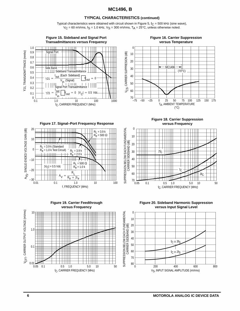
MC1496, B
6 MOTOROLA ANALOG IC DEVICE DATA
– 30
f, FREQUENCY (MHz)
20
10
0
– 10
– 20
0.1 1.0 10 1000.01
RL = 3.9 kRe = 500 Ω
RL = 3.9 kRe = 2.0 k
|VC| = 0.5 VdcRL = 500 ΩRe = 1.0 k
RL = 3.9 k (StandardRe = 1.0 k Test Circuit)
A
, SIN
GLE
-EN
DED
VO
LTAG
E G
AIN
(dB)
V S
1001.0
Side Band
0.3
0.4
01000
fC, CARRIER FREQUENCY (MHz)
0.6
0.91.0
10
0.8
0.7
0.1
0.2
0.5
0.1
21, T
RAN
SAD
MIT
TAN
CE
(mm
ho)
800
fC ± 3fS
800600400200VS, INPUT SIGNAL AMPLITUDE (mVrms)
fC ± 2fS
0
60
50
40
30
20
10
70
SUPP
RES
SIO
N B
ELO
W E
ACH
FU
ND
AMEN
TAL
CAR
RIE
R S
IDEB
AND
(dB)
fC
2fC
505.00.05 0.1 0.5 1.0 10
3fC
0
60
50
40
30
20
10
70
fC, CARRIER FREQUENCY (MHz)
SUPP
RES
SIO
N B
ELO
W E
ACH
FU
ND
AMEN
TAL
CAR
RIE
R S
IDEB
AND
(dB)
TA, AMBIENT TEMPERATURE(°C)
MC1496(70°C)
–75 –50
60
7550250–25
50
40
30
20
10
100 125 150 17570
CS
V
, C
ARR
IER
SU
PPR
ESIO
N (d
B)
AVRL
Re 2re
TYPICAL CHARACTERISTICS (continued)
Typical characteristics were obtained with circuit shown in Figure 5, fC = 500 kHz (sine wave),VC = 60 mVrms, fS = 1.0 kHz, VS = 300 mVrms, TA = 25°C, unless otherwise noted.
0.1
5010
10
1.0
0.011.0 5.00.05 0.1 0.5
fC, CARRIER FREQUENCY (MHz)
V
, C
ARR
IER
OU
TPU
T VO
LTAG
E (m
Vrm
s)C
FT
Signal Port0
Figure 15. Sideband and Signal PortTransadmittances versus Frequency
Figure 16. Carrier Suppressionversus Temperature
Figure 17. Signal–Port Frequency ResponseFigure 18. Carrier Suppression
versus Frequency
Figure 19. Carrier Feedthroughversus Frequency
Figure 20. Sideband Harmonic Suppressionversus Input Signal Level
γ
21IoutVin Vout 0 |VC| 0.5 Vdc
21Iout (Each Sideband)
Vin (Signal) Vout 0
Sideband Transadmittance
Signal Port Transadmittance
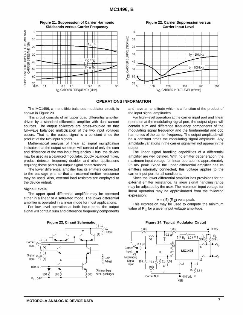
MC1496, B
7MOTOROLA ANALOG IC DEVICE DATA
500100 4003000 200VC, CARRIER INPUT LEVEL (mVrms)
fC = 10 MHz
0
60
50
40
30
20
10
70
CS
V
, C
ARR
IER
SU
PPR
ESSI
ON
(dB)
2fC ± fS
2fC ± 2fS
3fC ± fS
fC, CARRIER FREQUENCY (MHz)50101.0 5.00.05 0.1 0.5
0
60
50
40
30
20
10
70
SUPP
RES
SIO
N B
ELO
W E
ACH
FU
ND
AMEN
TAL
CAR
RIE
R S
IDEB
AND
(dB)
Figure 21. Suppression of Carrier HarmonicSidebands versus Carrier Frequency
Figure 22. Carrier Suppression versusCarrier Input Level
fC = 500 kHz
OPERATIONS INFORMATION
The MC1496, a monolithic balanced modulator circuit, isshown in Figure 23.
This circuit consists of an upper quad differential amplifierdriven by a standard differential amplifier with dual currentsources. The output collectors are cross–coupled so thatfull–wave balanced multiplication of the two input voltagesoccurs. That is, the output signal is a constant times theproduct of the two input signals.
Mathematical analysis of linear ac signal multiplicationindicates that the output spectrum will consist of only the sumand difference of the two input frequencies. Thus, the devicemay be used as a balanced modulator, doubly balanced mixer,product detector, frequency doubler, and other applicationsrequiring these particular output signal characteristics.
The lower differential amplifier has its emitters connectedto the package pins so that an external emitter resistancemay be used. Also, external load resistors are employed atthe device output.
Signal LevelsThe upper quad differential amplifier may be operated
either in a linear or a saturated mode. The lower differentialamplifier is operated in a linear mode for most applications.
For low–level operation at both input ports, the outputsignal will contain sum and difference frequency components
and have an amplitude which is a function of the product ofthe input signal amplitudes.
For high–level operation at the carrier input port and linearoperation at the modulating signal port, the output signal willcontain sum and difference frequency components of themodulating signal frequency and the fundamental and oddharmonics of the carrier frequency. The output amplitude willbe a constant times the modulating signal amplitude. Anyamplitude variations in the carrier signal will not appear in theoutput.
The linear signal handling capabilities of a differentialamplifier are well defined. With no emitter degeneration, themaximum input voltage for linear operation is approximately25 mV peak. Since the upper differential amplifier has itsemitters internally connected, this voltage applies to thecarrier input port for all conditions.
Since the lower differential amplifier has provisions for anexternal emitter resistance, its linear signal handling rangemay be adjusted by the user. The maximum input voltage forlinear operation may be approximated from the followingexpression:
V = (I5) (RE) volts peak.This expression may be used to compute the minimum
value of RE for a given input voltage amplitude.
SignalInput
CarrierInput
8 (+)
500500 50014VEE
Bias
VC
(Pin numbersper G package)
Vo,Output
(–) 12
2GainAdjust3
(+) 6
VS
10 (–)
4 (–)
1 (+)
5
–Vo
Re 1.0 k2
12 Vdc
RL3.9 k
+Vo
VEE–8.0 Vdc
6.8 kI5
14
0.1 µF
12
MC14966
8
1.0 k1.0 k
50 k
51
10 k10 k
0.1 µFCarrierInput
ModulatingSignalInput
VS
VC
Carrier Null
51
3
51
4110
5
RL3.9 k
Figure 23. Circuit Schematic Figure 24. Typical Modulator Circuit
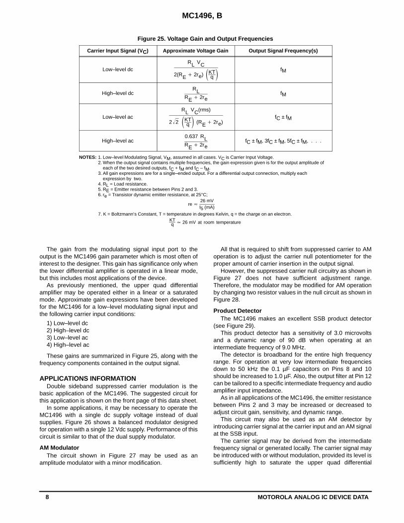
MC1496, B
8 MOTOROLA ANALOG IC DEVICE DATA
Figure 25. Voltage Gain and Output Frequencies
Carrier Input Signal (V C) Approximate Voltage Gain Output Signal Frequency(s)
Low–level dcRL VC
2(RE 2re) KTq
fM
High–level dcRL
RE 2refM
Low–level acRL VC(rms)
2 2 KTq (RE 2re)
fC ± fM
High–level ac0.637 RLRE 2re
fC ± fM, 3fC ± fM, 5fC ± fM, . . .
NOTES: 1. Low–level Modulating Signal, VM, assumed in all cases. VC is Carrier Input Voltage.2. When the output signal contains multiple frequencies, the gain expression given is for the output amplitude of
each of the two desired outputs, fC + fM and fC – fM.3. All gain expressions are for a single–ended output. For a differential output connection, multiply each
expression by two.4. RL = Load resistance.5. RE = Emitter resistance between Pins 2 and 3.6. re = Transistor dynamic emitter resistance, at 25°C;
re 26 mVI5 (mA)
7. K = Boltzmann′s Constant, T = temperature in degrees Kelvin, q = the charge on an electron.KTq 26 mV at room temperature
The gain from the modulating signal input port to theoutput is the MC1496 gain parameter which is most often ofinterest to the designer. This gain has significance only whenthe lower differential amplifier is operated in a linear mode,but this includes most applications of the device.
As previously mentioned, the upper quad differentialamplifier may be operated either in a linear or a saturatedmode. Approximate gain expressions have been developedfor the MC1496 for a low–level modulating signal input andthe following carrier input conditions:
1) Low–level dc2) High–level dc3) Low–level ac4) High–level ac
These gains are summarized in Figure 25, along with thefrequency components contained in the output signal.
APPLICATIONS INFORMATIONDouble sideband suppressed carrier modulation is the
basic application of the MC1496. The suggested circuit forthis application is shown on the front page of this data sheet.
In some applications, it may be necessary to operate theMC1496 with a single dc supply voltage instead of dualsupplies. Figure 26 shows a balanced modulator designedfor operation with a single 12 Vdc supply. Performance of thiscircuit is similar to that of the dual supply modulator.
AM ModulatorThe circuit shown in Figure 27 may be used as an
amplitude modulator with a minor modification.
All that is required to shift from suppressed carrier to AMoperation is to adjust the carrier null potentiometer for theproper amount of carrier insertion in the output signal.
However, the suppressed carrier null circuitry as shown inFigure 27 does not have sufficient adjustment range.Therefore, the modulator may be modified for AM operationby changing two resistor values in the null circuit as shown inFigure 28.
Product DetectorThe MC1496 makes an excellent SSB product detector
(see Figure 29).This product detector has a sensitivity of 3.0 microvolts
and a dynamic range of 90 dB when operating at anintermediate frequency of 9.0 MHz.
The detector is broadband for the entire high frequencyrange. For operation at very low intermediate frequenciesdown to 50 kHz the 0.1 µF capacitors on Pins 8 and 10should be increased to 1.0 µF. Also, the output filter at Pin 12can be tailored to a specific intermediate frequency and audioamplifier input impedance.
As in all applications of the MC1496, the emitter resistancebetween Pins 2 and 3 may be increased or decreased toadjust circuit gain, sensitivity, and dynamic range.
This circuit may also be used as an AM detector byintroducing carrier signal at the carrier input and an AM signalat the SSB input.
The carrier signal may be derived from the intermediatefrequency signal or generated locally. The carrier signal maybe introduced with or without modulation, provided its level issufficiently high to saturate the upper quad differential
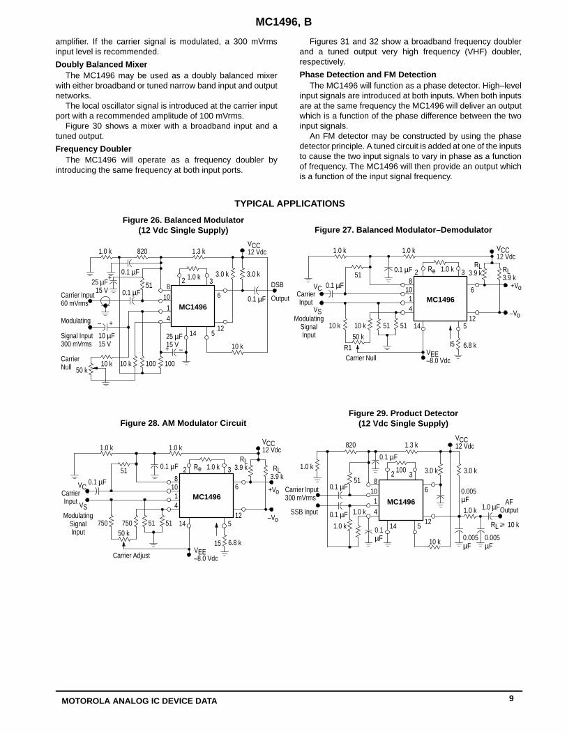
MC1496, B
9MOTOROLA ANALOG IC DEVICE DATA
amplifier. If the carrier signal is modulated, a 300 mVrmsinput level is recommended.
Doubly Balanced MixerThe MC1496 may be used as a doubly balanced mixer
with either broadband or tuned narrow band input and outputnetworks.
The local oscillator signal is introduced at the carrier inputport with a recommended amplitude of 100 mVrms.
Figure 30 shows a mixer with a broadband input and atuned output.
Frequency DoublerThe MC1496 will operate as a frequency doubler by
introducing the same frequency at both input ports.
Figures 31 and 32 show a broadband frequency doublerand a tuned output very high frequency (VHF) doubler,respectively.
Phase Detection and FM DetectionThe MC1496 will function as a phase detector. High–level
input signals are introduced at both inputs. When both inputsare at the same frequency the MC1496 will deliver an outputwhich is a function of the phase difference between the twoinput signals.
An FM detector may be constructed by using the phasedetector principle. A tuned circuit is added at one of the inputsto cause the two input signals to vary in phase as a functionof frequency. The MC1496 will then provide an output whichis a function of the input signal frequency.
VS
DSB
MC1496
VCC12 Vdc
–
R1
+
Carrier Input60 mVrms
CarrierInput
1.0 k1.0 k
Carrier Null
Carrier Adjust
1.0 k
Re 1.0 k2RL
3.9 k3 RL3.9 k
–Vo
+Vo
12
6
6.8 kI5VEE–8.0 Vdc
10 k10 k 51 51Modulating
SignalInput
VC
14 5
0.1 µF
0.1 µF
50 k
+ –
MC1496
Output
0.1 µF
0.1 µF0.1 µF
VCC12 Vdc
10 k 100 100
10 k
3.0 k 3.0 k1.0 k
1.3 k820
50 k10 k
10 µF15 V
Signal Input300 mVrms
Modulating
CarrierNull
+25 µF
15 V51
25 µF15 V
2 3
14 5
ModulatingSignalInput
VS
VC
1.0 µF
CarrierInput
50 k750 51 51750
VEE–8.0 Vdc
15 6.8 k
RL3.9 k
Re 1.0 k2 3
14 5
0.1 µF
–Vo
+Vo
VCC12 Vdc
51
51
1.0 k1.0 k
MC1496
2 3
14 5
MC1496
1.3 k820
1.0 k
Carrier Input300 mVrms
SSB Input
51100 3.0 k 3.0 k
0.005µF10 k
0.1µF
1.0 k
0.1 µF0.1 µF
0.1 µF
0.1 µF
VCC12 Vdc
AFOutput
RL 10 k
0.005µF
TYPICAL APPLICATIONS
1.0 k
8
41
10
12
6
12
6
12
6
RL3.9 k
8
41
10
8
41
108
41
10
Figure 26. Balanced Modulator(12 Vdc Single Supply) Figure 27. Balanced Modulator–Demodulator
Figure 28. AM Modulator CircuitFigure 29. Product Detector
(12 Vdc Single Supply)
1.0 k
0.005µF
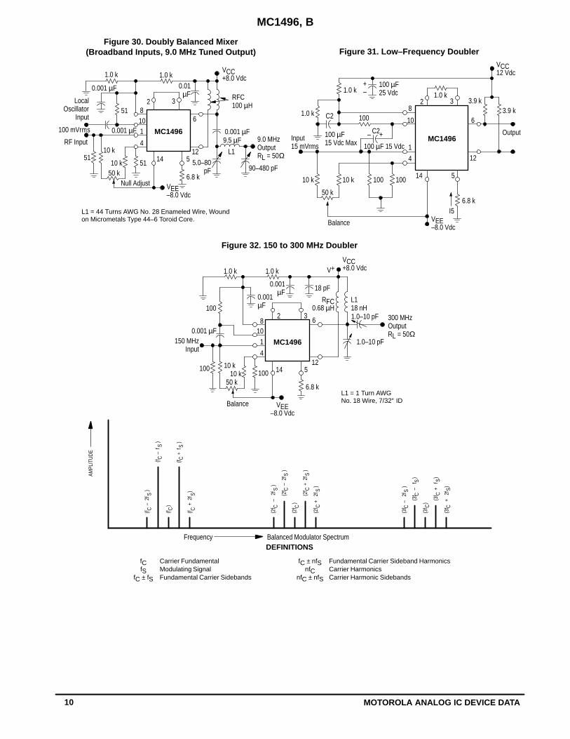
MC1496, B
10 MOTOROLA ANALOG IC DEVICE DATA
(f
+ 2
f )
C
S
C
S
C
S
RFC100 µH
(2f
– 2
f )
fCfS
fC ± fS
fC ± nfSnfC
nfC ± nfS
DEFINITIONS
Figure 30. Doubly Balanced Mixer(Broadband Inputs, 9.0 MHz Tuned Output) Figure 31. Low–Frequency Doubler
Frequency Balanced Modulator Spectrum
L1 = 44 Turns AWG No. 28 Enameled Wire, Woundon Micrometals Type 44–6 Toroid Core.
VCC+8.0 Vdc1.0 k1.0 k
Null Adjust
0.001 µF
512 3
5
6.8 kVEE–8.0 Vdc
10 k 5151
10 k
MC1496
0.001 µF
LocalOscillator
Input
RF Input
100 mVrms
50 k
0.001 µF9.5 µF
L1
5.0–80pF 90–480 pF
9.0 MHzOutputRL = 50Ω
0.01µF
VCC12 Vdc
3.9 k3.9 k
5
2 3
MC1496
6.8 kI5
VEE–8.0 Vdc
1.0 k
10 k 10 k
100
100
100 µF 15 Vdc
100 µF25 Vdc
+–
–+
100C2
100 µF15 Vdc Max
1.0 k
1.0 k
C2
50 k
Balance
Input15 mVrms
L1 = 1 Turn AWGNo. 18 Wire, 7/32″ IDBalance
MC1496
300 MHzOutputRL = 50Ω
1.0–10 pF
L118 nH
RFC0.68 µH
0.001µF
0.001µF
1.0 k1.0 k
VCC+8.0 Vdc
Output
100
0.001 µF150 MHz
Input
10 k10 k 100
50 k
2 3
18 pF
6.8 k
AMPL
ITU
DE
(f ) C
C
S
100
V+
VEE–8.0 Vdc
(f
– 2
f )
C
S
(f
– f
)
(f
+ f
)
(2f
–
2f
)
(2f
+ 2
f )
(2f
+
2f
)
(3f
–
2f
)
(3f
–
f )
(3f
)
(3f
+
f )
(3f
+
2f
)
C
C
S
C
S
C
S C
S
C
S C
S
C
S
(2f
) C
8
4
110
12
68
4
110
8
4
1
10
12
6
14 5
14
14
12
6
Figure 32. 150 to 300 MHz Doubler
Carrier FundamentalModulating SignalFundamental Carrier Sidebands
Fundamental Carrier Sideband HarmonicsCarrier HarmonicsCarrier Harmonic Sidebands
1.0–10 pF
Recommended


![ORIENTAÇÕES GERAIS MOSTRA LITERÁRIA MONTEIRO ......Conto: A pílula falante – Fragmento Monteiro Lobato [...] O doutor escolheu uma pílula falante e pôs-lhe na boca. – Engula](https://img.pdfslide.tips/doc/110x75/611b7e73ee4df278b86a4ad2/orientaes-gerais-mostra-literria-monteiro-conto-a-plula-falante.jpg)