1
LT1007/LT1037
sn100737 100737fbs
FEATURES DESCRIPTIO
U
APPLICATIO SU
TYPICAL APPLICATIO
U
Low Noise, High SpeedPrecision Operational Amplifiers
Guaranteed 4.5nV/√Hz 10Hz Noise Guaranteed 3.8nV/√Hz 1kHz Noise 0.1Hz to 10Hz Noise, 60nVP-P Typical Guaranteed 7 Million Min Voltage Gain, RL = 2k Guaranteed 3 Million Min Voltage Gain, RL = 600Ω Guaranteed 25µV Max Offset Voltage Guaranteed 0.6µV/°C Max Drift with Temperature Guaranteed 11V/µs Min Slew Rate (LT1037) Guaranteed 117dB Min CMRR
The LT®1007/LT1037 series features the lowest noiseperformance available to date for monolithic operationalamplifiers: 2.5nV/√Hz wideband noise (less than the noise ofa 400Ω resistor), 1/f corner frequency of 2Hz and 60nV peak-to-peak 0.1Hz to 10Hz noise. Low noise is combined withoutstanding precision and speed specifications: 10µV offsetvoltage, 0.2µV/°C drift, 130dB common mode and powersupply rejection, and 60MHz gain bandwidth product on thedecompensated LT1037, which is stable for closed-loopgains of 5 or greater.The voltage gain of the LT1007/LT1037 is an extremely high20 million driving a 2kΩ load and 12 million driving a 600Ωload to ±10V.In the design, processing and testing of the device, particularattention has been paid to the optimization of the entiredistribution of several key parameters. Consequently, thespecifications of even the lowest cost grades (the LT1007Cand the LT1037C) have been spectacularly improved com-pared to equivalent grades of competing amplifiers.The sine wave generator application shown below utilizes thelow noise and low distortion characteristics of the LT1037., LTC and LT are registered trademarks of Linear Technology Corporation.
Ultrapure 1kHz Sine Wave Generator
TIME (SEC)0 2 4 6 8 10
VOLT
AGE
NOIS
E (2
0nV/
DIV)
1007/37 TA02
Low Noise Signal Processing Microvolt Accuracy Threshold Detection Strain Gauge Amplifiers Direct Coupled Audio Gain Stages Sine Wave Generators Tape Head Preamplifiers Microphone Preamplifiers
1007/37 TA01
430Ω
OUTPUT
C
C R
R
6
2
3
#327 LAMP
–
+LT1037
f = 12πRC
R = 1591.5Ω ±0.1%C = 0.1µF ±0.1%
TOTAL HARMONIC DISTORTION = < 0.0025%NOISE = < 0.0001%AMPLITUDE = ±8VOUTPUT FREQUENCY = 1.000kHz FOR VALUES GIVEN ±0.4%
0.1Hz to 10Hz Noise
2
LT1007/LT1037
sn100737 100737fbs
ABSOLUTE MAXIMUM RATINGS
W WW U
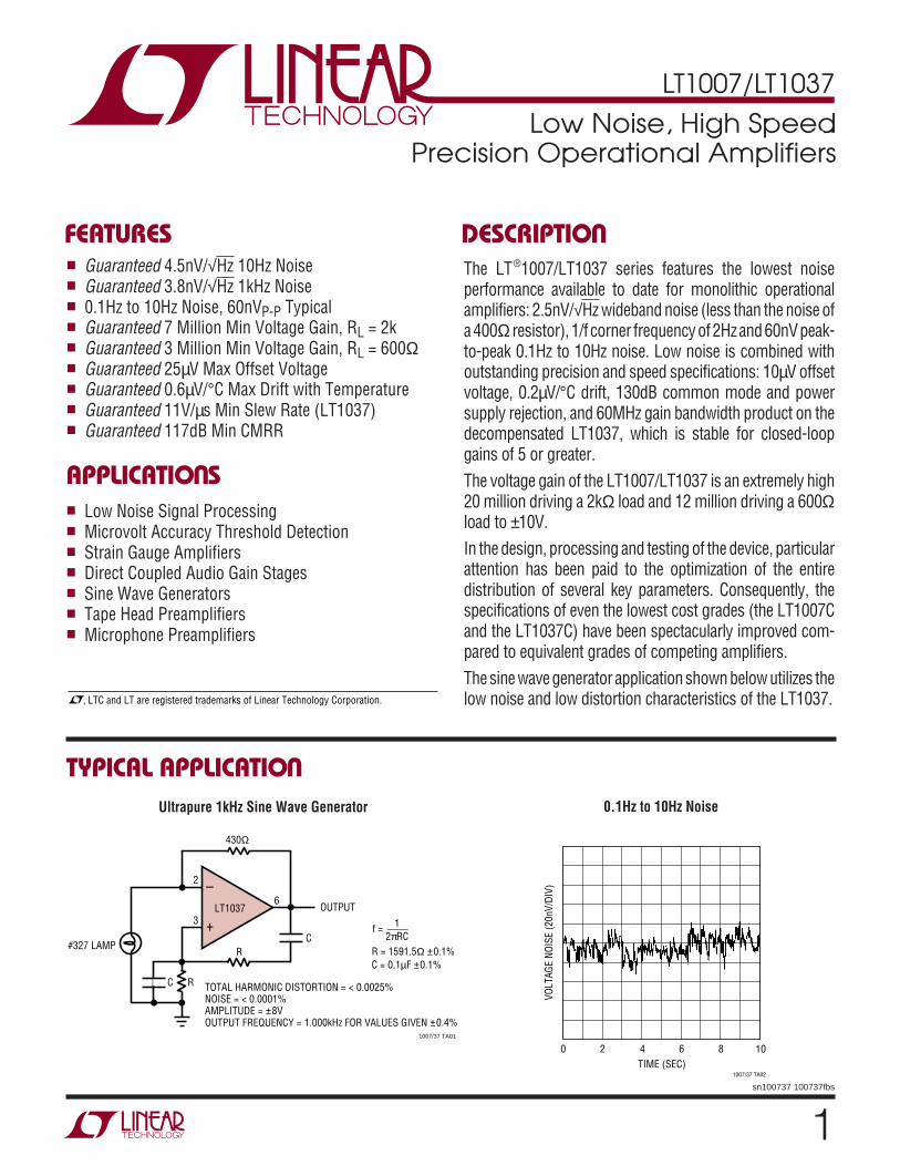
PACKAGE/ORDER INFORMATION
W UU
Supply Voltage ...................................................... ±22VInput Voltage ............................ Equal to Supply VoltageOutput Short-Circuit Duration .......................... IndefiniteDifferential Input Current (Note 9) ..................... ±25mAStorage Temperature Range ................. –65°C to 150°C
TOP VIEW
V+
VOS TRIM
VOSTRIM
–IN OUT
NC+IN
V– (CASE)
87
6
5
1
4
H PACKAGE8-LEAD TO-5 METAL CAN
–+
2
3
TJMAX = 150°C, θJA = 150°C/ W, θJC = 45°C/ W
1
2
3
4
8
7
6
5
TOP VIEW
VOSTRIM
VOSTRIMV+
OUT
NC
–IN
+IN
V–
–+
N8 PACKAGE8-LEAD PDIP
TOP VIEW
S8 PACKAGE8-LEAD PLASTIC SO
1
2
3
4
8
7
6
5
VOSTRIM
VOSTRIMV+
OUT
NC
–IN
+IN
V–
–
+
TJMAX = 150°C, θJA = 190°C/ W
ORDER PART NUMBER ORDER PART NUMBER ORDER PART NUMBER
10071007I
10371037I
LT1007ACN8LT1007CN8LT1007IN8
LT1037ACN8LT1037CN8LT1037IN8
LT1007ACHLT1007AMHLT1007CHLT1007MH
LT1037ACHLT1037AMHLT1037CHLT1037MH
TJMAX = 100°C, θJA = 130°C/ W (N8)
S8 PART MARKING
LT1007CS8LT1007IS8
LT1037CS8LT1037IS8
(Note 1)
Consult LTC Marketing for parts specified with wider operating temperature ranges.
Lead Temperature (Soldering, 10 sec.) ................. 300°COperating Temperature Range
LT1007/LT1037AC, C ............................. 0°C to 70°CLT1007/LT1037I ............................... –40°C to 85°CLT1007/LT1037AM, M (OBSOLETE) –55°C to 125°C
LT1007ACJ8LT1007AMJ8LT1007CJ8LT1007MJ8
LT1037ACJ8LT1037AMJ8LT1037CJ8LT1037MJ8
TJMAX = 150°C, θJA = 100°C/ W (J8)
J8 PACKAGELEAD CERDIP
OBSOLETE PACKAGE OBSOLETE PACKAGE
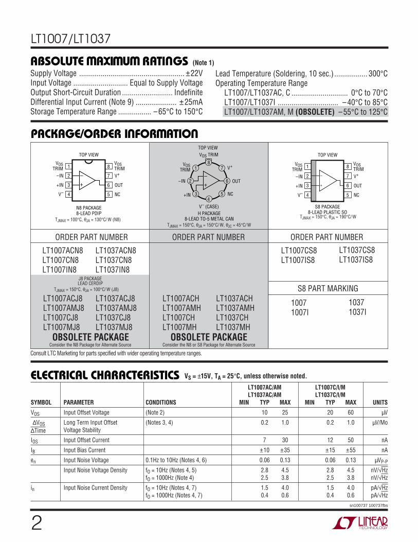
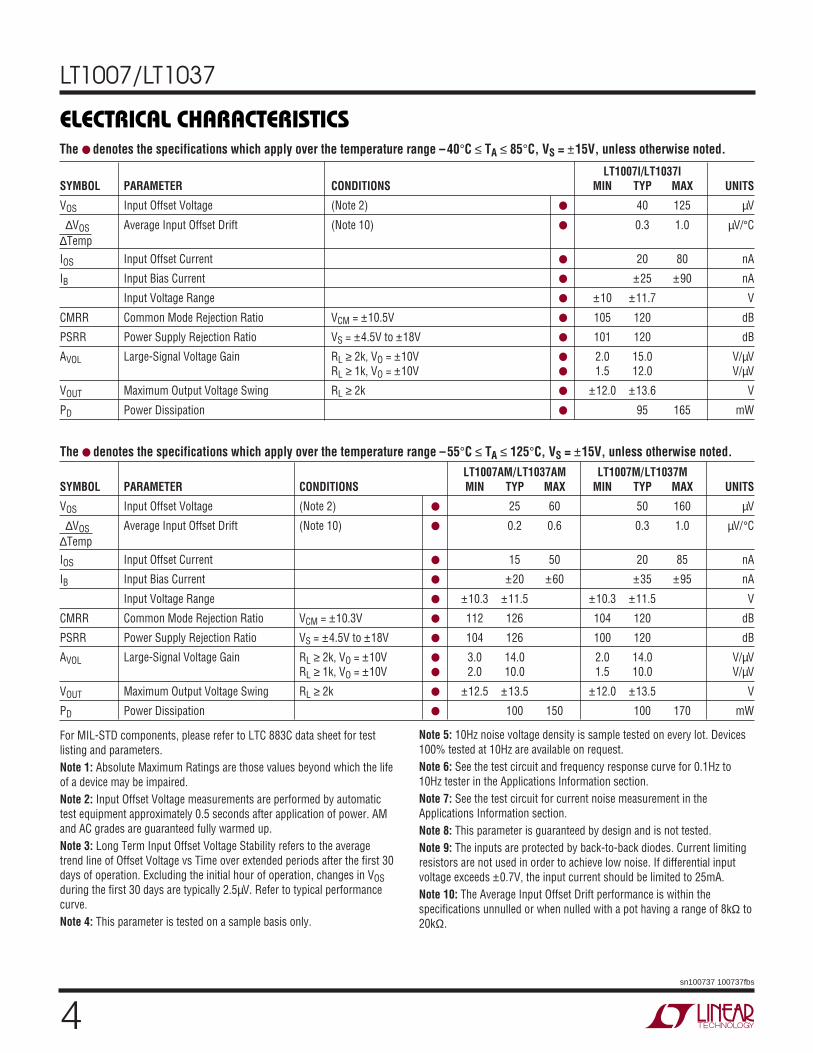
ELECTRICAL CHARACTERISTICS VS = ±15V, TA = 25°C, unless otherwise noted.
LT1007AC/AM LT1007C/I/MLT1037AC/AM LT1037C/I/M
SYMBOL PARAMETER CONDITIONS MIN TYP MAX MIN TYP MAX UNITS
VOS Input Offset Voltage (Note 2) 10 25 20 60 µV
∆VOS Long Term Input Offset (Notes 3, 4) 0.2 1.0 0.2 1.0 µV/Mo∆Time Voltage Stability
IOS Input Offset Current 7 30 12 50 nA
IB Input Bias Current ±10 ±35 ±15 ±55 nA
en Input Noise Voltage 0.1Hz to 10Hz (Notes 4, 6) 0.06 0.13 0.06 0.13 µVP-P
Input Noise Voltage Density fO = 10Hz (Notes 4, 5) 2.8 4.5 2.8 4.5 nV/√HzfO = 1000Hz (Note 4) 2.5 3.8 2.5 3.8 nV/√Hz
in Input Noise Current Density fO = 10Hz (Notes 4, 7) 1.5 4.0 1.5 4.0 pA/√HzfO = 1000Hz (Notes 4, 7) 0.4 0.6 0.4 0.6 pA/√Hz
Consider the N8 Package for Alternate Source Consider the N8 or S8 Package for Alternate Source
3
LT1007/LT1037
sn100737 100737fbs
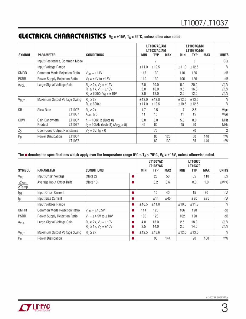
ELECTRICAL CHARACTERISTICS VS = ±15V, TA = 25°C, unless otherwise noted.
LT1007AC/AM LT1007C/I/MLT1037AC/AM LT1037C/I/M
SYMBOL PARAMETER CONDITIONS MIN TYP MAX MIN TYP MAX UNITS
Input Resistance, Common Mode 7 5 GΩInput Voltage Range ±11.0 ±12.5 ±11.0 ±12.5 V
CMRR Common Mode Rejection Ratio VCM = ±11V 117 130 110 126 dB
PSRR Power Supply Rejection Ratio VS = ±4V to ±18V 110 130 106 126 dB
AVOL Large-Signal Voltage Gain RL ≥ 2k, VO = ±12V 7.0 20.0 5.0 20.0 V/µVRL ≥ 1k, VO = ±10V 5.0 16.0 3.5 16.0 V/µVRL ≥ 600Ω, VO = ±10V 3.0 12.0 2.0 12.0 V/µV
VOUT Maximum Output Voltage Swing RL ≥ 2k ±13.0 ±13.8 ±12.5 ±13.5 VRL ≥ 600Ω ±11.0 ±12.5 ±10.5 ±12.5 V
SR Slew Rate LT1007 RL ≥ 2k 1.7 2.5 1.7 2.5 V/µsLT1037 AVCL ≥ 5 11 15 11 15 V/µs
GBW Gain Bandwidth LT1007 fO = 100kHz (Note 8) 5.0 8.0 5.0 8.0 MHzProduct LT1037 fO = 10kHz (Note 8) (AVCL ≥ 5) 45 60 45 60 MHz
ZO Open-Loop Output Resistance VO = 0V, IO = 0 70 70 ΩPD Power Dissipation LT1007 80 120 80 140 mW
LT1037 80 130 85 140 mW
LT1007AC LT1007CLT1037AC LT1037C
SYMBOL PARAMETER CONDITIONS MIN TYP MAX MIN TYP MAX UNITS
VOS Input Offset Voltage (Note 2) 20 50 35 110 µV
∆VOS Average Input Offset Drift (Note 10) 0.2 0.6 0.3 1.0 µV/°C∆TempIOS Input Offset Current 10 40 15 70 nA
IB Input Bias Current ±14 ±45 ±20 ±75 nA
Input Voltage Range ±10.5 ±11.8 ±10.5 ±11.8 V
CMRR Common Mode Rejection Ratio VCM = ±10.5V 114 126 106 120 dB
PSRR Power Supply Rejection Ratio VS = ±4.5V to ±18V 106 126 102 120 dB
AVOL Large-Signal Voltage Gain RL ≥ 2k, VO = ±10V 4.0 18.0 2.5 18.0 V/µVRL ≥ 1k, VO = ±10V 2.5 14.0 2.0 14.0 V/µV
VOUT Maximum Output Voltage Swing RL ≥ 2k ±12.5 ±13.6 ±12.0 ±13.6 V
PD Power Dissipation 90 144 90 160 mW
The denotes the specifications which apply over the temperature range 0°C ≤ TA ≤ 70°C, VS = ±15V, unless otherwise noted.
4
LT1007/LT1037
sn100737 100737fbs
The denotes the specifications which apply over the temperature range –40°C ≤ TA ≤ 85°C, VS = ±15V, unless otherwise noted.
ELECTRICAL CHARACTERISTICS
For MIL-STD components, please refer to LTC 883C data sheet for testlisting and parameters.Note 1: Absolute Maximum Ratings are those values beyond which the lifeof a device may be impaired.Note 2: Input Offset Voltage measurements are performed by automatictest equipment approximately 0.5 seconds after application of power. AMand AC grades are guaranteed fully warmed up.Note 3: Long Term Input Offset Voltage Stability refers to the averagetrend line of Offset Voltage vs Time over extended periods after the first 30days of operation. Excluding the initial hour of operation, changes in VOSduring the first 30 days are typically 2.5µV. Refer to typical performancecurve.Note 4: This parameter is tested on a sample basis only.
Note 5: 10Hz noise voltage density is sample tested on every lot. Devices100% tested at 10Hz are available on request.Note 6: See the test circuit and frequency response curve for 0.1Hz to10Hz tester in the Applications Information section.Note 7: See the test circuit for current noise measurement in theApplications Information section.Note 8: This parameter is guaranteed by design and is not tested.Note 9: The inputs are protected by back-to-back diodes. Current limitingresistors are not used in order to achieve low noise. If differential inputvoltage exceeds ±0.7V, the input current should be limited to 25mA.Note 10: The Average Input Offset Drift performance is within thespecifications unnulled or when nulled with a pot having a range of 8kΩ to20kΩ.
The denotes the specifications which apply over the temperature range –55°C ≤ TA ≤ 125°C, VS = ±15V, unless otherwise noted.
LT1007I/LT1037ISYMBOL PARAMETER CONDITIONS MIN TYP MAX UNITS
VOS Input Offset Voltage (Note 2) 40 125 µV
∆VOS Average Input Offset Drift (Note 10) 0.3 1.0 µV/°C∆TempIOS Input Offset Current 20 80 nA
IB Input Bias Current ±25 ±90 nA
Input Voltage Range ±10 ±11.7 V
CMRR Common Mode Rejection Ratio VCM = ±10.5V 105 120 dB
PSRR Power Supply Rejection Ratio VS = ±4.5V to ±18V 101 120 dB
AVOL Large-Signal Voltage Gain RL ≥ 2k, VO = ±10V 2.0 15.0 V/µVRL ≥ 1k, VO = ±10V 1.5 12.0 V/µV
VOUT Maximum Output Voltage Swing RL ≥ 2k ±12.0 ±13.6 V
PD Power Dissipation 95 165 mW
LT1007AM/LT1037AM LT1007M/LT1037MSYMBOL PARAMETER CONDITIONS MIN TYP MAX MIN TYP MAX UNITS
VOS Input Offset Voltage (Note 2) 25 60 50 160 µV
∆VOS Average Input Offset Drift (Note 10) 0.2 0.6 0.3 1.0 µV/°C∆TempIOS Input Offset Current 15 50 20 85 nA
IB Input Bias Current ±20 ±60 ±35 ±95 nA
Input Voltage Range ±10.3 ±11.5 ±10.3 ±11.5 V
CMRR Common Mode Rejection Ratio VCM = ±10.3V 112 126 104 120 dB
PSRR Power Supply Rejection Ratio VS = ±4.5V to ±18V 104 126 100 120 dB
AVOL Large-Signal Voltage Gain RL ≥ 2k, VO = ±10V 3.0 14.0 2.0 14.0 V/µVRL ≥ 1k, VO = ±10V 2.0 10.0 1.5 10.0 V/µV
VOUT Maximum Output Voltage Swing RL ≥ 2k ±12.5 ±13.5 ±12.0 ±13.5 V
PD Power Dissipation 100 150 100 170 mW
5
LT1007/LT1037
sn100737 100737fbs
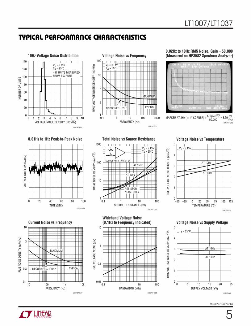
TYPICAL PERFORMANCE CHARACTERISTICS
UW
VOLTAGE NOISE DENSITY (nV/√Hz)0
NUM
BER
OF U
NITS
140
120
100
80
60
40
20
01 5 7
1007/37 G01
4 9 102 3 6 8
VS = ±15VTA = 25°C497 UNITS MEASUREDFROM SIX RUNS
FREQUENCY (Hz)1
1
3
RMS
VOLT
AGE
NOIS
E DE
NSIT
Y (n
V/√H
z)
10
30
100
10 1000
1007/37 G02
0.1 100
VS = ±15VTA = 25°C
1/f CORNER = 2Hz
MAXIMUM
TYPICAL
Voltage Noise vs Frequency
0.01Hz to 1Hz Peak-to-Peak Noise
TIME (SEC)0 20 40 60 80 100
VOLT
AGE
NOIS
E (2
0nV/
DIV)
1007/37 G04
FREQUENCY (Hz)10
0.1
0.3
3
1
10
100 1k 10k
1007/37 G07
RMS
NOIS
E DE
NSIT
Y (p
A/√H
z)
1/f CORNER = 120Hz
MAXIMUM
TYPICAL
TEMPERATURE (°C)–50
5
4
3
2
1
00 50 75
1007/37 G06
–25 25 100 125
AT 10Hz
VS = ±15V
AT 1kHzRM
S VO
LTAG
E NO
ISE
DENS
ITY
(nV/
√Hz)
10Hz Voltage Noise Distribution
Total Noise vs Source Resistance Voltage Noise vs Temperature
SOURCE RESISTANCE (kΩ)0.1
1
10
100
1000
1 10 100
1007/37 G05
TOTA
L NO
ISE
DENS
ITY
(nV/
√Hz)
VS = ±15VTA = 25°C
SOURCE RESISTANCE = 2R
R
R
AT 1kHz
AT 10Hz
RESISTORNOISE ONLY
Current Noise vs Frequency
BANDWIDTH (kHz)0.1
0.01
RMS
VOLT
AGE
NOIS
E (µ
V)
0.1
1
10
1 10 100
1007/37 G08
Wideband Voltage Noise(0.1Hz to Frequency Indicated)
SUPPLY VOLTAGE (±V)0
5
4
3
2
1
020
1007/37 G09
5 10 15 25
RMS
VOLT
AGE
NOIS
E DE
NSIT
Y (n
V/√H
z)
AT 10Hz
TA = 25°C
AT 1kHz
Voltage Noise vs Supply Voltage
0.02Hz to 10Hz RMS Noise. Gain = 50,000(Measured on HP3582 Spectrum Analyzer)
MARKER AT 2Hz ( = 1/f CORNER) = 179µV/√Hz50,000
nV√Hz
= 3.59
1007/37 G03
6
LT1007/LT1037
sn100737 100737fbs
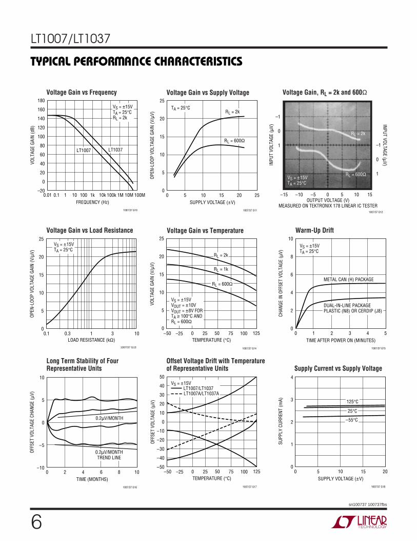
TYPICAL PERFORMANCE CHARACTERISTICS
UW
FREQUENCY (Hz)0.01
VOLT
AGE
GAIN
(dB)
180
160
140
120
100
80
60
40
20
0
–20
1007/37 G10
0.1 1 10 100 1k 10k 100k 1M 10M 100M
VS = ±15VTA = 25°CRL = 2k
LT1037LT1007
Voltage Gain, RL = 2k and 600Ω
SUPPLY VOLTAGE (±V)0
OPEN
-LOO
P VO
LTAG
E GA
IN (V
/µV)
25
20
15
10
5
020
1007/37 G11
5 10 15 25
TA = 25°CRL = 2k
RL = 600Ω
TIME AFTER POWER ON (MINUTES)0
CHAN
GE IN
OFF
SET
VOLT
AGE
(µV)
10
8
6
4
2
04
1007/37 G15
1 2 3 5
VS = ±15VTA = 25°C
DUAL-IN-LINE PACKAGEPLASTIC (N8) OR CERDIP (J8)
METAL CAN (H) PACKAGE
Voltage Gain vs Frequency Voltage Gain vs Supply Voltage
Voltage Gain vs Load Resistance
LOAD RESISTANCE (kΩ)0.1 0.3 3
OPEN
-LOO
P VO
LTAG
E GA
IN (V
/µV)
25
20
15
10
5
01 10
1007/37 G13
VS = ±15VTA = 25°C
Warm-Up Drift
TEMPERATURE (°C)
VOLT
AGE
GAIN
(V/µ
V)
–50
25
20
15
10
5
00 50 75
1007/37 G14
–25 25 100 125
RL = 2k
RL = 1k
RL = 600Ω
VS = ±15VVOUT = ±10VVOUT = ±8V FORTA ≥ 100°C ANDRL = 600Ω
Voltage Gain vs Temperature
TIME (MONTHS)0
OFFS
ET V
OLTA
GE C
HANG
E (µ
V)
10
5
0
–5
–108
1007/37 G16
2 4 6 10
0.2µV/MONTH
0.2µV/MONTHTREND LINE
Long Term Stability of FourRepresentative Units
SUPPLY VOLTAGE (±V)0
SUPP
LY C
URRE
NT (m
A)
20
1007/37 G18
5 10 15
4
3
2
1
0
125°C
25°C
–55°C
Supply Current vs Supply VoltageOffset Voltage Drift with Temperatureof Representative Units
TEMPERATURE (°C)–50
OFFS
ET V
OLTA
GE (µ
V)
50
40
30
20
10
0
–10
–20
–30
–40
–500 50 75
1007/37 G17
–25 25 100 125
VS = ±15V
LT1007A/LT1037ALT1007/LT1037
–1
0
1 –1
0
1VS = ±15VTA = 25°C
INPU
T VO
LTAG
E (µ
V)
INPUT VOLTAGE (µV)
–15 –10 –5 0 5 10 15OUTPUT VOLTAGE (V)
MEASURED ON TEKTRONIX 178 LINEAR IC TESTER1007/37 G12
RL = 2k
RL = 600Ω
7
LT1007/LT1037
sn100737 100737fbs
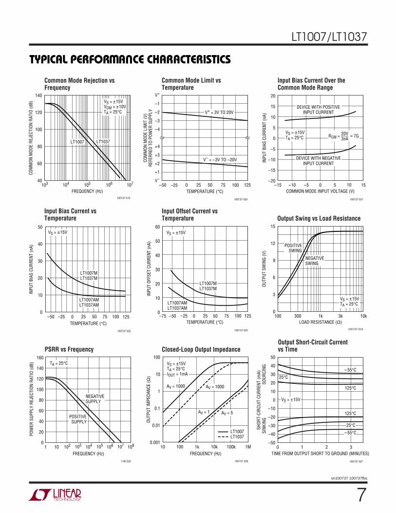
TYPICAL PERFORMANCE CHARACTERISTICS
UW
FREQUENCY (Hz)
COM
MON
MOD
E RE
JECT
ION
RATI
O (d
B)
140
120
100
80
60
40103 105 106 107
1007/37 G19
104
VS = ±15VVCM = ±10VTA = 25°C
LT1037LT1007
Common Mode Rejection vsFrequency
Input Bias Current vsTemperature
TEMPERATURE (°C)–50
INPU
T BI
AS C
URRE
NT (n
A)
1007/37 G22
0 50 100
50
40
30
20
10
0–25 25 75 125
VS = ±15V
LT1007MLT1037M
LT1007AMLT1037AM
TIME FROM OUTPUT SHORT TO GROUND (MINUTES)0
SHOR
T-CI
RCUI
T CU
RREN
T (m
A)SO
URCI
NGSI
NKIN
G
50
40
30
20
10
0
–10
–20
–30
–40
–501 2
1007/37 G27
3
–55°C
–55°C
125°C
125°C
25°C
25°C
VS = ±15V
Output Short-Circuit Currentvs Time
LOAD RESISTANCE (Ω)100 300 3k
OUTP
UT S
WIN
G (V
)
15
12
9
6
3
01k 10k
1007/37 G24
VS = ±15VTA = 25°C
POSITIVESWING
NEGATIVESWING
Output Swing vs Load Resistance
COMMON MODE INPUT VOLTAGE (V)–15 –10
INPU
T BI
AS C
URRE
NT (n
A)
–5 50 10 15
1007/37 G21
20
15
10
5
0
–5
–10
–15
–20
DEVICE WITH NEGATIVEINPUT CURRENT
DEVICE WITH POSITIVEINPUT CURRENT
VS = ±15VTA = 25°C RCM = ≈ 7G20V
3nA
Input Bias Current Over theCommon Mode Range
TEMPERATURE (°C)–50
COM
MON
MOD
E LI
MIT
(V)
REFE
RRED
TO
POW
ER S
UPPL
Y
V+
–1
–2
–3
–4
+4
+3
+2
+1
V–
0 50 75
1007/37 G20
–25 25 100 125
V+ = 3V TO 20V
V– = –3V TO –20V
Common Mode Limit vsTemperature
TEMPERATURE (°C)–75
INPU
T OF
FSET
CUR
RENT
(nA)
–50 0 25–25 50 75 100 125
1007/37 G23
60
50
40
30
20
10
0
VS = ±15V
LT1007MLT1037M
LT1007AMLT1037AM
Input Offset Current vsTemperature
Closed-Loop Output Impedance
FREQUENCY (Hz)10
OUTP
UT IM
PEDA
NCE
(Ω)
100
10
1
0.1
0.01
0.001100k
1007/37 G26
100 1k 10k 1M
VS = ±15VTA = 25°CIOUT = 1mA
AV = 1000 AV = 1000
AV = 1 AV = 5
LT1007LT1037
FREQUENCY (Hz)1
POW
ER S
UPPL
Y RE
JECT
ION
RATI
O (d
B)
1195 G25
10210 103 104 105 106 107 108
160
140
120
100
80
60
40
20
0
TA = 25°C
NEGATIVESUPPLY
POSITIVESUPPLY
PSRR vs Frequency
8
LT1007/LT1037
sn100737 100737fbs
TYPICAL PERFORMANCE CHARACTERISTICS
UW
TEMPERATURE (°C)–50
SLEW
RAT
E (V
/ µs)
P
HASE
MAR
GIN
(DEG
) GAIN BANDWIDTH PROCUCT, fO = 10kHz (M
Hz)
70
60
50
20
15
10
70
60
50
0 50 75
1007/37 G30
–25 25 100 125
SLEW
GBW
VS = ±15VCL = 100pF
PHASE MARGIN
50mV
0V
–50mV
AVCL = 5VS = ±15VCL = 15pF 1007/37 G28
LT1037 Small-SignalTransient Response
LT1037 Phase Margin, GainBandwidth Product, Slew Rate vsTemperature
10V
0V
– 10V
AVCL = 5VS = ±15V 1007/37 G29
LT1037 Large-Signal Response
FREQUENCY (MHz)0.1
VOLT
AGE
GAIN
(dB)
40
30
20
10
0
–10
PHASE SHIFT (DEG)
90
100
110
120
130
140
150
160
170
180
1901 10 100
1007/37 G32
VS = ±15VTA = 25°CCL = 100pF
GAIN
PHASE
TEMPERATURE (°C)–50
SLEW
RAT
E (V
/µs)
PHA
SE M
ARGI
N (D
EG)
GAIN BANDWIDTH PROCUCT, fO = 100kHz (M
Hz)
70
60
50
3
2
1
9
8
7
0 50 75
1007/37 G33
–25 25 100 125
SLEW
GBW
VS = ±15VCL = 100pF
PHASE MARGIN
FREQUENCY (MHz)0.1
VOLT
AGE
GAIN
(dB)
50
40
30
20
10
0
PHASE SHIFT (DEG)
90
100
110
120
130
140
150
160
170
180
1901 10 100
1007/37 G31
AV = 5
VS = ±15VTA = 25°CCL = 100pF
GAIN
PHASE
LT1037 Gain, Phase Shiftvs Frequency
LT1007 Gain, Phase Shiftvs Frequency
50mV
0V
–50mV
AVCL = 1VS = ±15VCL = 15pF 1007/37 G34
FREQUENCY (Hz)
28
24
20
16
12
8
4
01k 100k 1M 10M
1007/37 G36
10k
PEAK
-TO-
PEAK
OUT
PUT
VOLT
AGE
(V) VS = ±15V
TA = 25°C
LT1037LT1007
Maximum Undistorted Outputvs Frequency
5V
0V
– 5V
AVCL = –1VS = ±15V 1007/37 G35
LT1007 Small-SignalTransient Response LT1007 Large-Signal Response
LT1007 Phase Margin, GainBandwidth Product, Slew Rate vsTemperature
9
LT1007/LT1037
sn100737 100737fbs
APPLICATIONS INFORMATION
WU UU
General
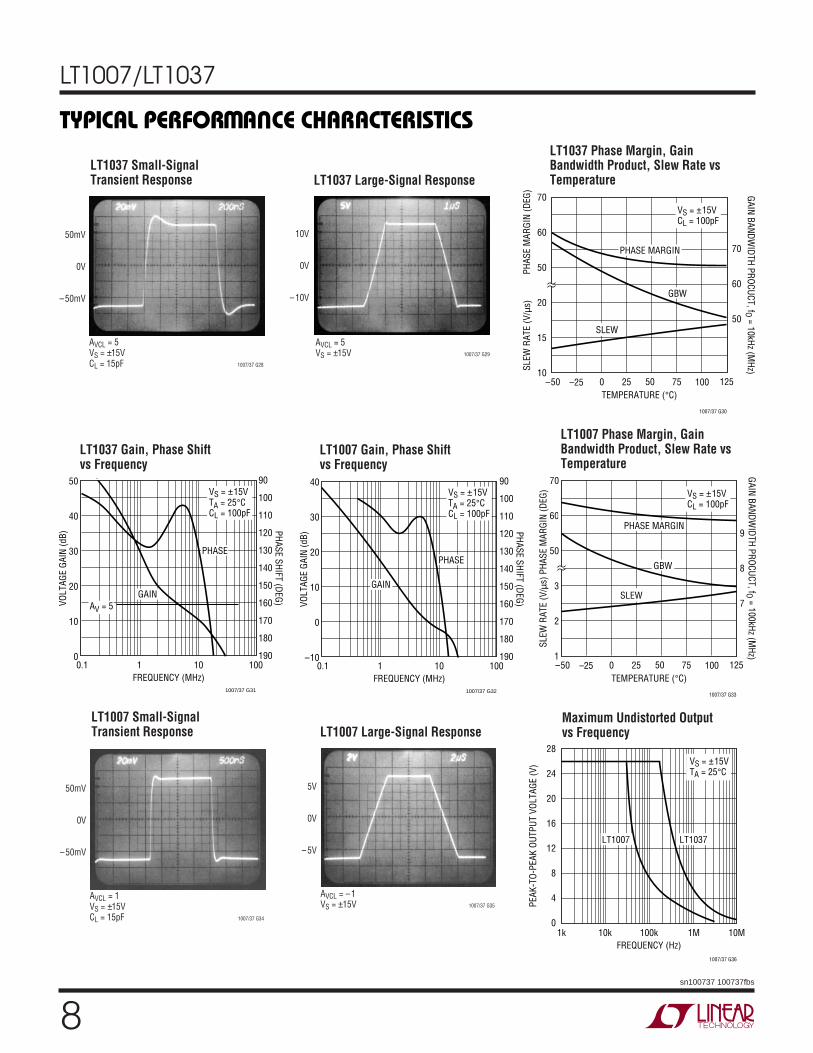
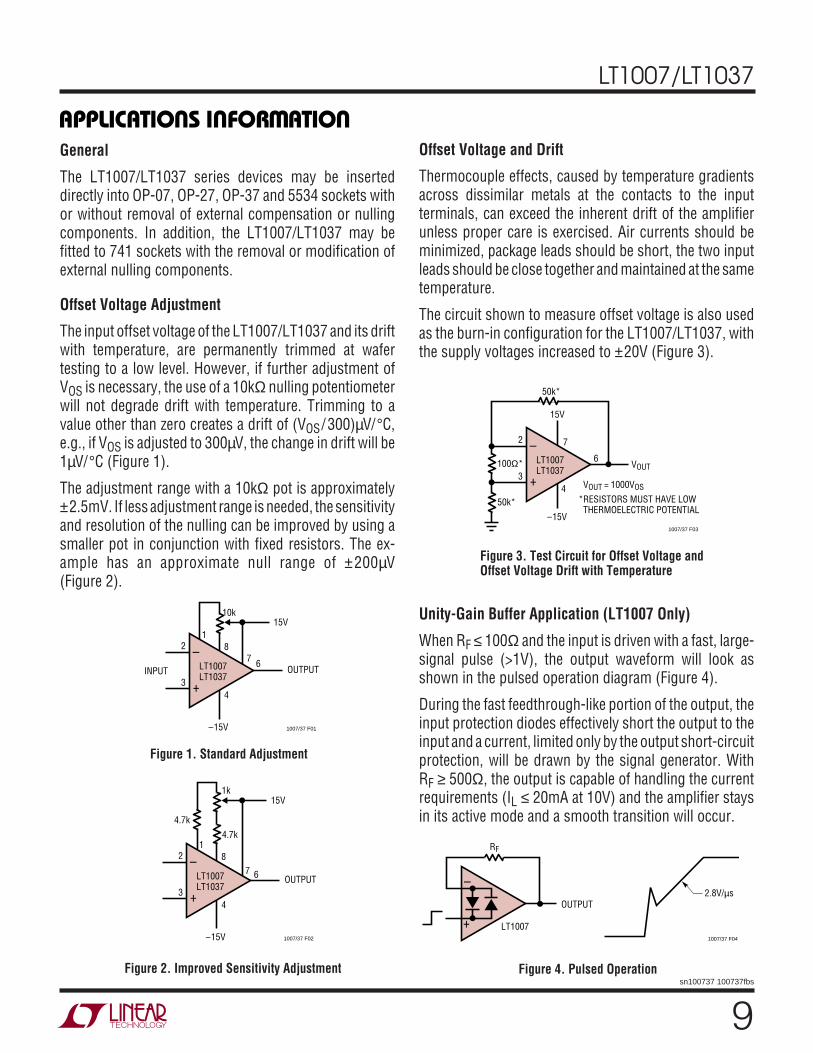
The LT1007/LT1037 series devices may be inserteddirectly into OP-07, OP-27, OP-37 and 5534 sockets withor without removal of external compensation or nullingcomponents. In addition, the LT1007/LT1037 may befitted to 741 sockets with the removal or modification ofexternal nulling components.
Offset Voltage Adjustment
The input offset voltage of the LT1007/LT1037 and its driftwith temperature, are permanently trimmed at wafertesting to a low level. However, if further adjustment ofVOS is necessary, the use of a 10kΩ nulling potentiometerwill not degrade drift with temperature. Trimming to avalue other than zero creates a drift of (VOS/300)µV/°C,e.g., if VOS is adjusted to 300µV, the change in drift will be1µV/°C (Figure 1).
The adjustment range with a 10kΩ pot is approximately±2.5mV. If less adjustment range is needed, the sensitivityand resolution of the nulling can be improved by using asmaller pot in conjunction with fixed resistors. The ex-ample has an approximate null range of ±200µV(Figure 2).
Offset Voltage and Drift
Thermocouple effects, caused by temperature gradientsacross dissimilar metals at the contacts to the inputterminals, can exceed the inherent drift of the amplifierunless proper care is exercised. Air currents should beminimized, package leads should be short, the two inputleads should be close together and maintained at the sametemperature.
The circuit shown to measure offset voltage is also usedas the burn-in configuration for the LT1007/LT1037, withthe supply voltages increased to ±20V (Figure 3).
Figure 2. Improved Sensitivity Adjustment
1007/37 F02
1k
4.7k
OUTPUT
87 6
4
12
3
15V
–15V
–
+LT1007LT1037
4.7k
1007/37 F01
10k
OUTPUTINPUT
87 6
4
12
3
15V
–15V
–
+LT1007LT1037
Figure 1. Standard Adjustment
Unity-Gain Buffer Application (LT1007 Only)
When RF ≤ 100Ω and the input is driven with a fast, large-signal pulse (>1V), the output waveform will look asshown in the pulsed operation diagram (Figure 4).
During the fast feedthrough-like portion of the output, theinput protection diodes effectively short the output to theinput and a current, limited only by the output short-circuitprotection, will be drawn by the signal generator. WithRF ≥ 500Ω, the output is capable of handling the currentrequirements (IL ≤ 20mA at 10V) and the amplifier staysin its active mode and a smooth transition will occur.
1007/37 F04
LT1007
–
+
RF
OUTPUT2.8V/µs
Figure 4. Pulsed Operation
1007/37 F03
VOUT
VOUT = 1000VOS
*RESISTORS MUST HAVE LOW THERMOELECTRIC POTENTIAL
7
6
4
2
3
15V
–15V
–
+LT1007LT1037
50k*
100Ω*
50k*
Figure 3. Test Circuit for Offset Voltage andOffset Voltage Drift with Temperature
10
LT1007/LT1037
sn100737 100737fbs
APPLICATIONS INFORMATION
WU UU
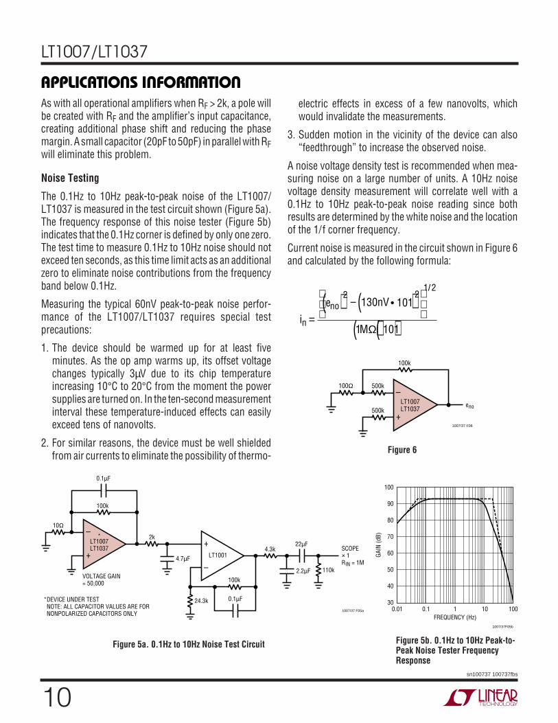
As with all operational amplifiers when RF > 2k, a pole willbe created with RF and the amplifier’s input capacitance,creating additional phase shift and reducing the phasemargin. A small capacitor (20pF to 50pF) in parallel with RFwill eliminate this problem.
Noise Testing
The 0.1Hz to 10Hz peak-to-peak noise of the LT1007/LT1037 is measured in the test circuit shown (Figure 5a).The frequency response of this noise tester (Figure 5b)indicates that the 0.1Hz corner is defined by only one zero.The test time to measure 0.1Hz to 10Hz noise should notexceed ten seconds, as this time limit acts as an additionalzero to eliminate noise contributions from the frequencyband below 0.1Hz.
Measuring the typical 60nV peak-to-peak noise perfor-mance of the LT1007/LT1037 requires special testprecautions:
1. The device should be warmed up for at least fiveminutes. As the op amp warms up, its offset voltagechanges typically 3µV due to its chip temperatureincreasing 10°C to 20°C from the moment the powersupplies are turned on. In the ten-second measurementinterval these temperature-induced effects can easilyexceed tens of nanovolts.
2. For similar reasons, the device must be well shieldedfrom air currents to eliminate the possibility of thermo-
electric effects in excess of a few nanovolts, whichwould invalidate the measurements.
3. Sudden motion in the vicinity of the device can also“feedthrough” to increase the observed noise.
A noise voltage density test is recommended when mea-suring noise on a large number of units. A 10Hz noisevoltage density measurement will correlate well with a0.1Hz to 10Hz peak-to-peak noise reading since bothresults are determined by the white noise and the locationof the 1/f corner frequency.
Current noise is measured in the circuit shown in Figure 6and calculated by the following formula:
ie nV
Mn
no=
( ) − ( )
( )( )
2 21 2
130 101
1 101
•/
Ω
FREQUENCY (Hz)
100
90
80
70
60
50
40
300.01 1 10 100
1007/37F05b
0.1
GAIN
(dB)
1007/37 F05a
10Ω
0.1µF
4.7µF
VOLTAGE GAIN= 50,000
24.3k
100k
–
+
–
+*
LT1007LT1037
LT1001
2k
4.3k
110k
100k
SCOPE× 1RIN = 1M
*DEVICE UNDER TEST NOTE: ALL CAPACITOR VALUES ARE FOR NONPOLARIZED CAPACITORS ONLY
2.2µF
0.1µF
22µF
Figure 5a. 0.1Hz to 10Hz Noise Test Circuit
1007/37 F06
100Ω
100k
–
+LT1007LT1037
500k
500keno
Figure 6
Figure 5b. 0.1Hz to 10Hz Peak-to-Peak Noise Tester FrequencyResponse
11
LT1007/LT1037
sn100737 100737fbs
The LT1007/LT1037 achieve their low noise, in part, byoperating the input stage at 120µA versus the typical 10µAof most other op amps. Voltage noise is inversely propor-tional while current noise is directly proportional to thesquare root of the input stage current. Therefore, theLT1007/LT1037’s current noise will be relatively high. Atlow frequencies, the low 1/f current noise corner fre-quency (≈120Hz) minimizes current noise to some extent.
In most practical applications, however, current noise willnot limit system performance. This is illustrated in theTotal Noise vs Source Resistance plot in the TypicalPerformance Characteristics section, where:
Total Noise = [(voltage noise)2 + (current noise • RS)2 +(resistor noise)2]1/2
Three regions can be identified as a function of sourceresistance:
(i) RS ≤ 400Ω. Voltage noise dominates
(ii) 400Ω ≤ RS ≤ 50k at 1kHz
400Ω ≤ RS ≤ 8k at 10Hz
(iii) RS > 50k at 1kHz
RS > 8k at 10Hz
Clearly the LT1007/LT1037 should not be used in region(iii), where total system noise is at least six times higherthan the voltage noise of the op amp, i.e., the low voltagenoise specification is completely wasted.
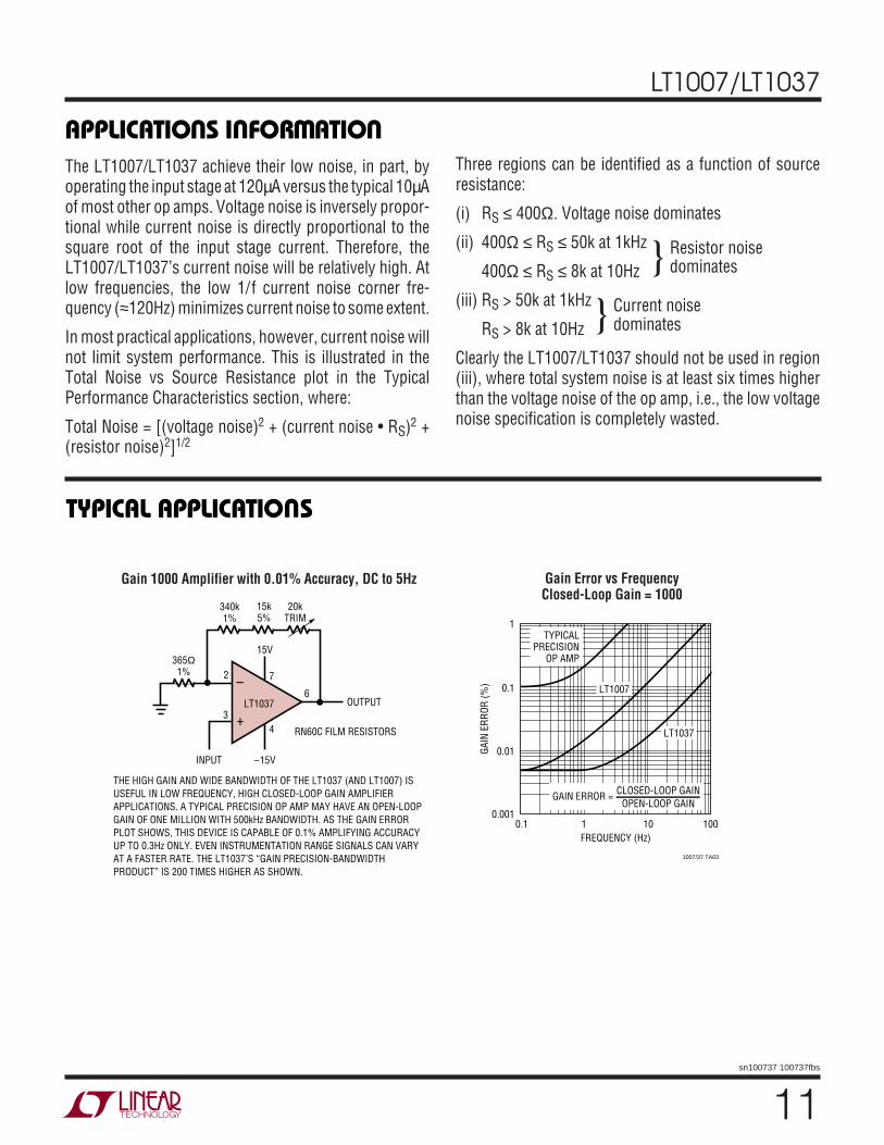
TYPICAL APPLICATIONS
U
1007/37 TA03
365Ω1%
15k5%
20kTRIM
–
+LT1037
2
15V
–15VINPUT
3
7
6
4
OUTPUT
RN60C FILM RESISTORS
340k1%
THE HIGH GAIN AND WIDE BANDWIDTH OF THE LT1037 (AND LT1007) IS USEFUL IN LOW FREQUENCY, HIGH CLOSED-LOOP GAIN AMPLIFIER APPLICATIONS. A TYPICAL PRECISION OP AMP MAY HAVE AN OPEN-LOOP GAIN OF ONE MILLION WITH 500kHz BANDWIDTH. AS THE GAIN ERROR PLOT SHOWS, THIS DEVICE IS CAPABLE OF 0.1% AMPLIFYING ACCURACY UP TO 0.3Hz ONLY. EVEN INSTRUMENTATION RANGE SIGNALS CAN VARY AT A FASTER RATE. THE LT1037’S “GAIN PRECISION-BANDWIDTH PRODUCT” IS 200 TIMES HIGHER AS SHOWN.
FREQUENCY (Hz)0.1
0.001
GAIN
ERR
OR (%
)
0.01
0.1
1
1 10 100
TYPICALPRECISION
OP AMP
LT1007
LT1037
GAIN ERROR = CLOSED-LOOP GAINOPEN-LOOP GAIN
Gain 1000 Amplifier with 0.01% Accuracy, DC to 5Hz Gain Error vs FrequencyClosed-Loop Gain = 1000
Resistor noisedominates
Current noisedominates
APPLICATIONS INFORMATION
WU UU
12
LT1007/LT1037
sn100737 100737fbs
TYPICAL APPLICATIONS
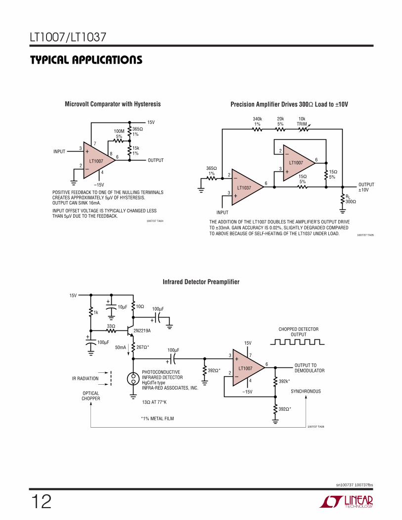
U
Infrared Detector Preamplifier
1007/37 TA08
IR RADIATION
OPTICALCHOPPER
–
+LT1007
50mA
15V
6
4
73
2
OUTPUT TODEMODULATOR
SYNCHRONOUS
CHOPPED DETECTOROUTPUT
PHOTOCONDUCTIVEINFRARED DETECTORHgCdTe typeINFRA-RED ASSOCIATES, INC.
100µF
392k*
15V
–15V
+
+
100µF10µF
+
392Ω*
392Ω*
267Ω*
2N2219A33Ω
10Ω1k
+100µF
13Ω AT 77°K
*1% METAL FILM
Precision Amplifier Drives 300Ω Load to ±10V
1007/37 TA05
365Ω1%
20k5%
10kTRIM
–
+LT1037
–
+LT1007
2
INPUT
3
2
3
6
6
OUTPUT±10V
15Ω5%
15Ω5%
RL300Ω
340k1%
THE ADDITION OF THE LT1007 DOUBLES THE AMPLIFIER’S OUTPUT DRIVE TO ±33mA. GAIN ACCURACY IS 0.02%, SLIGHTLY DEGRADED COMPARED TO ABOVE BECAUSE OF SELF-HEATING OF THE LT1037 UNDER LOAD.
Microvolt Comparator with Hysteresis
1007/37 TA04
OUTPUT
POSITIVE FEEDBACK TO ONE OF THE NULLING TERMINALSCREATES APPROXIMATELY 5µV OF HYSTERESIS. OUTPUT CAN SINK 16mA.
INPUT OFFSET VOLTAGE IS TYPICALLY CHANGED LESSTHAN 5µV DUE TO THE FEEDBACK.
7
86
42
3INPUT
–15V
15V
–
+LT1007
100M5%
365Ω1%
15k1%
13
LT1007/LT1037
sn100737 100737fbs
TYPICAL APPLICATIONS
U
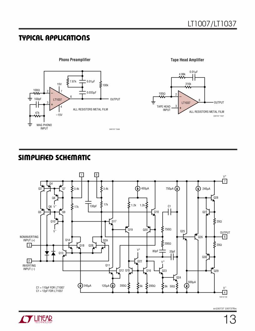
Phono Preamplifier
1007/37 TA06
100Ω –
+LT1037
MAG PHONOINPUT
7
6
43
2
7.87k15V
–15V
OUTPUT
ALL RESISTORS METAL FILM
0.01µF
0.033µF
100pF
47k
100k
Tape Head Amplifier
1007/37 TA07
100Ω –
+LT1037
TAPE HEADINPUT
6
3
2
OUTPUT
ALL RESISTORS METAL FILM
0.01µF4.99k
316k
SI PLIFIED SCHE ATIC
W W
Q1A
Q10
Q6
Q4
Q2B
Q15
Q2A
Q1B
INVERTINGINPUT (–)
C1 = 110pF FOR LT1007C1 = 12pF FOR LT1037
NONINVERTINGINPUT (+)
3
1 8
7
6
V–
V–
V+
V+
4V–
1007/37 SD
V+
OUTPUT
Q8
3.4k 3.4k
17k17k 1.2k
750Ω
20Ω
20Ω200Ω
50Ω200Ω200Ω 6k6k
80pF 20pF
C11.2k
Q20
130pF
Q17
Q18
Q25
Q24
Q23Q16Q12
Q22Q30
Q28
Q26
Q29
Q27
450µA 240µA
500µA120µA240µA
750µA
Q19
Q11
Q13
Q7
2
Q3
Q5 Q9
14
LT1007/LT1037
sn100737 100737fbs
PACKAGE DESCRIPTION
U
H Package8-Lead TO-5 Metal Can (.200 Inch PCD)
(Reference LTC DWG # 05-08-1320)
J8 Package8-Lead CERDIP (Narrow .300 Inch, Hermetic)
(Reference LTC DWG # 05-08-1110)
45°TYP
0.050(1.270)
MAX
0.016 – 0.021**(0.406 – 0.533)
0.010 – 0.045*(0.254 – 1.143)
SEATINGPLANE
0.040(1.016)
MAX 0.165 – 0.185(4.191 – 4.699)
GAUGEPLANE
REFERENCEPLANE
0.500 – 0.750(12.700 – 19.050)
0.305 – 0.335(7.747 – 8.509)
0.335 – 0.370(8.509 – 9.398)
DIA
0.200(5.080)
TYP
0.027 – 0.045(0.686 – 1.143)
0.027 – 0.034(0.686 – 0.864)
0.110 – 0.160(2.794 – 4.064)
INSULATINGSTANDOFF
H8(TO-5) 0.200 PCD 0595
LEAD DIAMETER IS UNCONTROLLED BETWEEN THE REFERENCE PLANE AND 0.045" BELOW THE REFERENCE PLANE
FOR SOLDER DIP LEAD FINISH, LEAD DIAMETER IS0.016 – 0.024
(0.406 – 0.610)
*
**
J8 1298
0.014 – 0.026(0.360 – 0.660)
0.200(5.080)
MAX
0.015 – 0.060(0.381 – 1.524)
0.1253.175MIN
0.100(2.54)BSC
0.300 BSC(0.762 BSC)
0.008 – 0.018(0.203 – 0.457)
0° – 15°
0.005(0.127)
MIN
0.405(10.287)
MAX
0.220 – 0.310(5.588 – 7.874)
1 2 3 4
8 7 6 5
0.025(0.635)
RAD TYP0.045 – 0.068
(1.143 – 1.727)FULL LEAD
OPTION
0.023 – 0.045(0.584 – 1.143)
HALF LEADOPTION
CORNER LEADS OPTION (4 PLCS)
0.045 – 0.065(1.143 – 1.651)NOTE: LEAD DIMENSIONS APPLY TO SOLDER DIP/PLATE
OR TIN PLATE LEADS
OBSOLETE PACKAGES
15
LT1007/LT1037
sn100737 100737fbs
Information furnished by Linear Technology Corporation is believed to be accurate and reliable.However, no responsibility is assumed for its use. Linear Technology Corporation makes no represen-tation that the interconnection of its circuits as described herein will not infringe on existing patent rights.
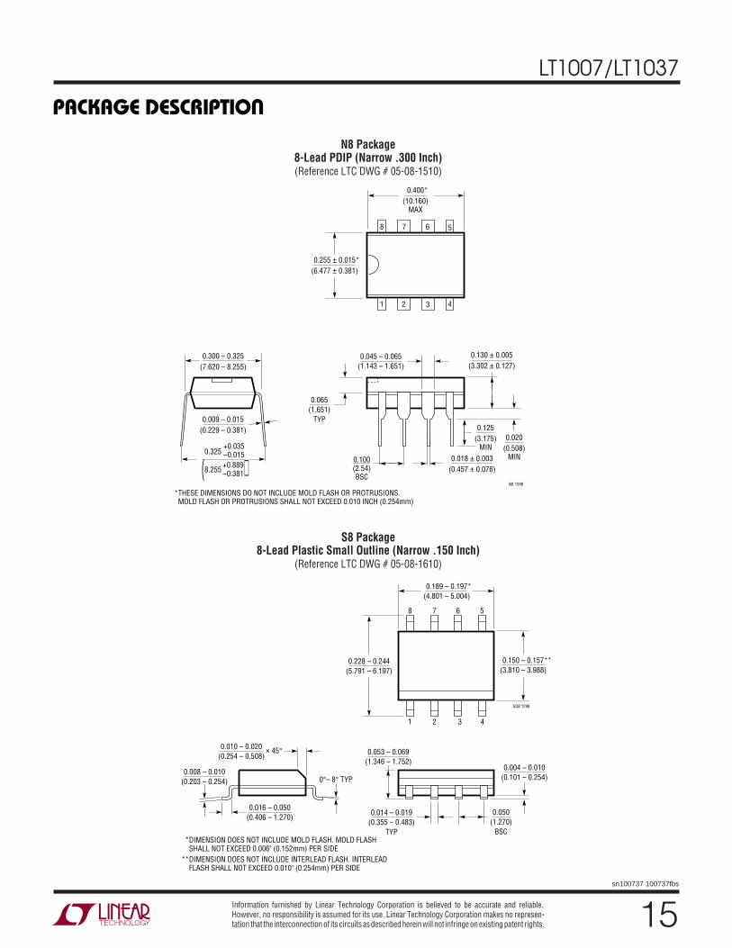
PACKAGE DESCRIPTION
U
N8 Package8-Lead PDIP (Narrow .300 Inch)(Reference LTC DWG # 05-08-1510)
S8 Package8-Lead Plastic Small Outline (Narrow .150 Inch)
(Reference LTC DWG # 05-08-1610)
N8 1098
0.100(2.54)BSC
0.065(1.651)
TYP
0.045 – 0.065(1.143 – 1.651)
0.130 ± 0.005(3.302 ± 0.127)
0.020(0.508)
MIN0.018 ± 0.003(0.457 ± 0.076)
0.125(3.175)
MIN
1 2 3 4
8 7 6 5
0.255 ± 0.015*(6.477 ± 0.381)
0.400*(10.160)
MAX
0.009 – 0.015(0.229 – 0.381)
0.300 – 0.325(7.620 – 8.255)
0.325+0.035–0.015+0.889–0.3818.255( )
*THESE DIMENSIONS DO NOT INCLUDE MOLD FLASH OR PROTRUSIONS. MOLD FLASH OR PROTRUSIONS SHALL NOT EXCEED 0.010 INCH (0.254mm)
0.016 – 0.050(0.406 – 1.270)
0.010 – 0.020(0.254 – 0.508)
× 45°
0°– 8° TYP0.008 – 0.010
(0.203 – 0.254)
SO8 1298
0.053 – 0.069(1.346 – 1.752)
0.014 – 0.019(0.355 – 0.483)
TYP
0.004 – 0.010(0.101 – 0.254)
0.050(1.270)
BSC
1 2 3 4
0.150 – 0.157**(3.810 – 3.988)
8 7 6 5
0.189 – 0.197*(4.801 – 5.004)
0.228 – 0.244(5.791 – 6.197)
DIMENSION DOES NOT INCLUDE MOLD FLASH. MOLD FLASH SHALL NOT EXCEED 0.006" (0.152mm) PER SIDEDIMENSION DOES NOT INCLUDE INTERLEAD FLASH. INTERLEAD FLASH SHALL NOT EXCEED 0.010" (0.254mm) PER SIDE
*
**

16
LT1007/LT1037
sn100737 100737fbs
LT/CPI 1101 1.5K REV B • PRINTED IN USA
LINEAR TECHNOLOGY CORPORATION 1985
Strain Gauge Signal Conditioner with Bridge Excitation
6
4
73
2
7.5V
7.5V
–7.5V
6
4
7
–7.5V
1007/37 TA09
–
+LT1007
–
+LT1007
6
4
73
3
2
2
350ΩBRIDGE
OUTPUT0V TO 10V
301k*
301k*
GAINTRIM50k
ZEROTRIM10k
REFERENCEOUT
1µF
15V
–15V
499Ω*
5k2.5V
LT1009
–
+LT1007 *RN60C FILM RESISTOR
THE LT1007 IS CAPABLE OF PROVIDING EXCITATION CURRENTDIRECTLY TO BIAS THE 350Ω BRIDGE AT 5V. WITH ONLY 5V ACROSSTHE BRIDGE (AS OPPOSED TO THE USUAL 10V) TOTAL POWERDISSIPATION AND BRIDGE WARM-UP DRIFT IS REDUCED. THE BRIDGEOUTPUT SIGNAL IS HALVED, BUT THE LT1007 CAN AMPLIFY THE REDUCED SIGNAL ACCURATELY.
RELATED PARTSPART NUMBER DESCRIPTION COMMENTS
LT1028 Ultralow Noise Precision Op Amp Lowest Noise 0.85nV/√Hz
LT1115 Ultralow Noise, Low distortion Audio Op Amp 0.002% THD, Max Noise 1.2mV/√Hz
LT1124/LT1125 Dual/Quad Low Noise, High Speed Precision Op Amps Similar to LT1007
LT1126/LT1127 Dual/Quad Decompensated Low Noise, High Speed Precision Op Amps Similar to LT1037
LT1498/LT1499 10MHz, 5V/µs, Dual/Quad Rail-to-Rail Input and OutputPrecision C-LoadTM Op Amps
C-Load is a trademark of Linear Technology Corporation.
U
TYPICAL APPLICATIO
Linear Technology Corporation1630 McCarthy Blvd., Milpitas, CA 95035-7417(408) 432-1900 FAX: (408) 434-0507 www.linear.com
Recommended