Large delay-bandwidth product and tuning of slow light pulse in
photonic crystal coupled waveguide Toshihiko Baba 1, 2 *, Takashi Kawasaki 1, 2, Hirokazu Sasaki 1, 2,
Jun Adachi 1, and Daisuke Mori 1, 2
1 Yokohama National University, Department of Electrical and Computer Engineering 79-5 Tokiwadai, Hodogayaku, Yokohama 240-8501, Japan
2 CREST, Japan Science and Technology Agency 5 Sanban-cho, Chiyodaku, Tokyo 102-0075, Japan
*Corresponding author: [email protected]
Abstract: This paper reports two advances in a slow light device consisting of chirped photonic crystal slab coupled waveguide on SOI substrate. One is concerning the delay-bandwidth product, indicating the buffering capacity of the device. We experimentally evaluated a record high value of 57 (a 40 ps delay and a 1.4 THz bandwidth). We also observed ~1 ps wide optical pulse transmission in the cross-correlation measurement. Regarding the pulse as a signal and considering the broadening of the pulse width due to the imperfect dispersion compensation in the device, storage of more than 12 signal bits was confirmed. The other is a wide-range tuning of the pulse delay. We propose a technique for externally controlling the chirping to permit variable delay. We demonstrate tuning of the pulse delay up to 23 ps, corresponding to a ~7 mm extension of the free space length.
©2008 Optical Society of America
OCIS codes: (230.3990) Micro-optical devices; (230.3120) Integrated optics devices
References and links
1. E. Parra and J. R. Lowell, “Toward applications of slow light technology,” Opt. Photonics News 18, 40-45 (2007).
2. M. Notomi, K. Yamada, A. Shinya, J. Takahashi, C. Takahashi, and I. Yokohama, “Extremely large group-velocity dispersion of line-defect waveguides in photonic crystal slabs,” Phys. Rev. Lett. 87, 253902 (2001).
3. M. Notomi, A. Shinya, S. Mitsugi, E. Kuramochi, and H. Ryu, “Waveguides, resonators and their coupled elements in photonic crystal slabs,” Opt. Express 12, 1551-1561 (2004).
4. T. Asano, K. Kiyota, D. Kumamoto, B. S. Song, and S. Noda, “Time-domain measurement of picosecond light-pulse propagation in a two-dimensional photonic crystal-slab waveguide,” Appl. Phys. Lett. 84, 4690-4692 (2004).
5. Y. A. Vlasov, M. O’Boyle, H. F. Hamann, and S. J. McNab, “Active control of slow light on a chip with photonic crystal waveguides,” Nature 438, 65-69 (2005).
6. H. Gersen, T. J. Karle, R. J. P. Engelen, W. Bogaerts, J. P. Korterik, N. F. van Hulst, N. F., T. F. Krauss, and L. Kuipers, “Real-space observation of ultraslow light in photonic crystal waveguides,” Phys. Rev. Lett. 94, 073903 (2005).
7. C. E. Finlayson, F. Cattaneo, N. M. B. Perney, J. J. Baumberg, M. C. Netti, M. E. Zoorob, M. D. B. Charlton, and G. J. Parker, “Slow light and chromatic temporal dispersion in photonic crystal waveguides using femtosecond time of flight,” Phys. Rev. E 73, 016619 (2006).
8. L. H. Frandsen, A. V. Lavrinenko, J. Fage-Pedersen, and P. I. Borel, “Photonic crystal waveguides with semislow light and tailored dispersion properties,” Opt. Express 14, 9444-9446 (2006).
9. T. Baba and D. Mori, “Slowlight engineering in photonic crystals,” J. Phys. D 40, 2659-2665 (2007). 10. M. D. Settle, R. J. P. Engelen, M. Salib, A. Michaeli, L. Kuipers and T. F. Krauss, “Flatband slow light in
photonic crystals featuring spatial pulse compression and terahertz bandwidth,” Opt. Express 15, 219-226 (2007).
11. F. Xia, L. Sekaric, and Y. Vlasov, “Ultracompact optical buffers on a silicon chip,” Nature Photon. 1, 65-71 (2007).
12. D. Mori, S. Kubo, H. Sasaki, and T. Baba, “Experimental demonstration of wideband dispersion-compensated slow light by a chirped photonic crystal directional coupler,” Opt. Express 15, 5264-5270 (2007).
#95680 - $15.00 USD Received 1 May 2008; revised 5 Jun 2008; accepted 5 Jun 2008; published 6 Jun 2008
(C) 2008 OSA 9 June 2008 / Vol. 16, No. 12 / OPTICS EXPRESS 9245
13. S. Kubo, D. Mori, and T. Baba, “Low-group-velocity and low-dispersion slow light in photonic crystal waveguides,” Opt. Lett. 32, 2981-2983 (2007).
14. R. S. Tucker, P-C. Ku, and C. J. Chang-Hasnain, “Slow-light optical buffers-capabilities and fundamental limitations,” J. Lightwave Technol. 23, 4046-4066 (2005).
15. D. A. B. Miller, “Fundamental limit to linear one-dimensional slow light structures,” Phys. Rev. Lett. 99, 203903 (2007).
16. D. Mori and T. Baba, “Dispersion-controlled optical group delay device by chirped photonic crystal waveguides,” Appl. Phys. Lett. 85, 1101-1103 (2004).
17. R. J. P. Engelen, Y. Sugimoto, Y. Watanabe, J. P. Korterik, N. F. van Hulst, K. Asakawa, and L. Kuipers, “The effect of higher-order dispersion on slow light propagation in photonic crystal waveguides,” Opt. Express 14, 1658-1672 (2006).
18. D. Mori and T. Baba, “Wideband and low dispersion slow light by chirped photonic crystal coupled waveguide,” Opt. Express 13, 9398-9408 (2005).
19. S. C. Huang, M. Kato, E. Kuramochi, C. P. Lee, and M. Notomi, “Time-domain and spectral-domain investigation of inflection-point slow-light modes in photonic crystal coupled waveguides,” Opt. Express 15, 3543-3549 (2007).
20. T. Kawasaki, D. Mori, and T. Baba, “Experimental observation of slow light in photonic crystal coupled waveguides,” Opt. Express 15, 10274-10281 (2007).
21. M. F. Yanik, and S. Fan, “Stopping light all optically,” Phys. Rev. Lett. 92, 083901 (2004). 22. T. Tanabe, M. Notomi, E. Kuramochi, A. Shinya, and H. Taniyama, “Trapping and delaying photons for one
nanosecond in an ultrasmall high-Q photonic-crystal nanocavity,” Nat. Photonics 1, 49-52 (2007). 23. Y. Tanaka, J. Upham, T. Nagashima, T. Sugiya, T. Asano, and S. Noda, “Dynamic control of the Q factor in
a photonic crystal nanocavity,” Nat. Mater. 6, 862-865 (2007). 24. J. K. Poon, L. Zhu, G. A. De Rose, and A. Yariv, “Transmission and group delay of microring coupled-
resonator optical waveguides,” Opt. Lett. 31, 456-458 (2006). 25. T. Baba, D. Mori, K. Inoshita, and Y. Kuroki, “Light localization in line defect photonic crystal
waveguides,” IEEE J. Quantum Electron. 10, 484-491 (2004).
Optical buffering and time-domain processing are key technologies in the next-generation peta-bit network traffic exploiting sophisticated photonic packet routing. Slow light with a greatly reduced group velocity is being intensively studied for high-speed continuous tuning of optical delays (see, for example [1]). In general, slow light is generated by a large linear dispersion in a particular material or structure. Highly dispersive photonic nanostructures such as photonic crystals are effective for room-temperature operation and on-chip integration of slow-light devices [2−13]. Here, the delay is essentially constrained by the frequency bandwidth. The delay-bandwidth product (DBP) is a critical index indicating the buffering capacity of slow-light devices [14, 15]. So far, it has been limited to being less than 30 (see, for example [10]) mainly because of insufficient slow down, limited bandwidth, and/or large nonlinear dispersions (particularly the group-velocity dispersion, GVD) [16, 17]. Also, the variable delay has been only observed in a narrow tuning range of ~1 ps against semi-continuous-wave light [5]. In this paper, we report great advances for a wideband GVD-free slow-light device in a photonic crystal coupled waveguide (PCCW) with a chirped structure [18−20].
Devices that generate slow light can be categorized into two types: those whose parameters are time-dependent and time-independent [14]. Devices without dynamic parameters (referred to as static slow light) simply reduce the group velocity of light υg ≡ c/ng, where c is the light velocity in vacuum and ng is the group index that indicates the slowdown factor. The DBP (= ΔtΔf, where Δt is the delay and Δf is the bandwidth) is proportional to the number of signal bits that are buffered in a slow-light device; the DBP is 2.5 times the number of signal bits when a signal bit consists of an ideal Gaussian or square second hyperbolic pulse. The Δt of static slow light is constrained by the DBP. Static slow light devices are space saving since the light is compressed in space by a factor of ng. Slow light generated by devices with dynamic parameters (dynamic slow light) breaks the DBP constraint and can achieve the complete stopping of light [21]. It is space consuming because light is not compressed but stopped preserving its envelope distribution. Therefore, the two-step slowdown process from static to dynamic slow light is considered to be the ultimate goal since it eliminates all constraints in time, frequency and space. In most studies, however, up until now it has only been possible to achieve a Δf of less than a few 10 GHz and a DBP of less than 10 for static
#95680 - $15.00 USD Received 1 May 2008; revised 5 Jun 2008; accepted 5 Jun 2008; published 6 Jun 2008
(C) 2008 OSA 9 June 2008 / Vol. 16, No. 12 / OPTICS EXPRESS 9246
slow light; these are obstacles in achieving the ultimate goal. The first part of this paper describes the improvement in these values we have obtained by using a PCCW.
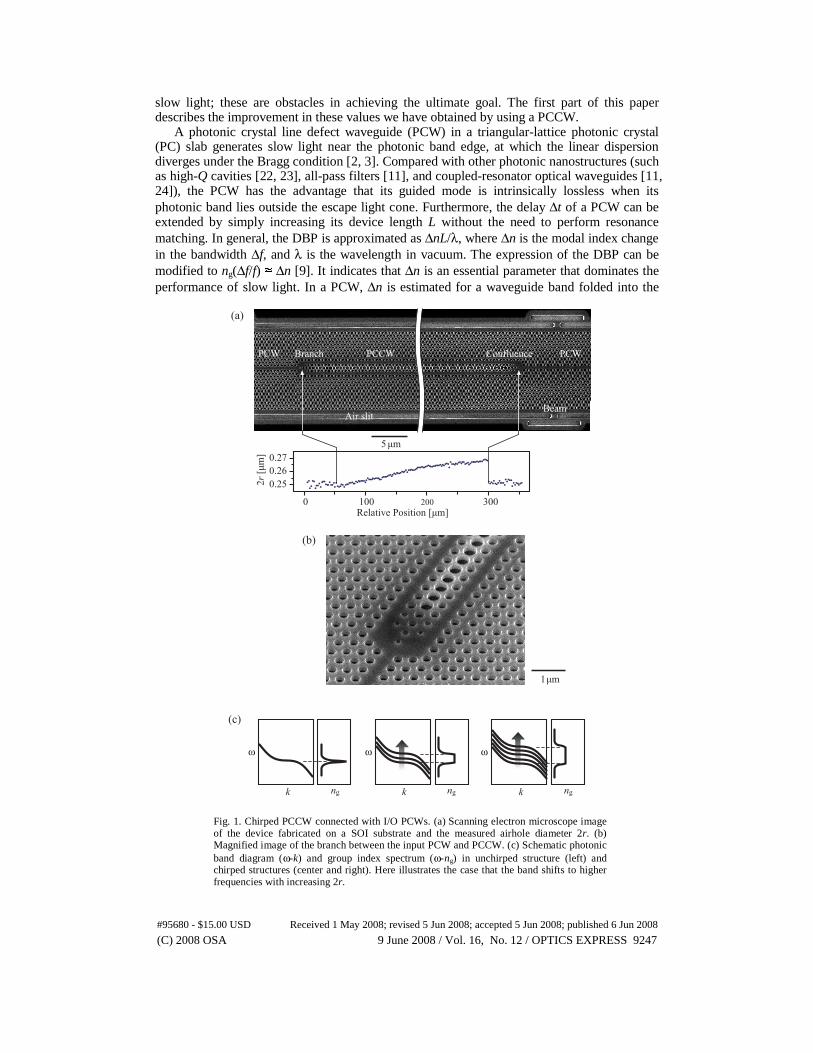
A photonic crystal line defect waveguide (PCW) in a triangular-lattice photonic crystal (PC) slab generates slow light near the photonic band edge, at which the linear dispersion diverges under the Bragg condition [2, 3]. Compared with other photonic nanostructures (such as high-Q cavities [22, 23], all-pass filters [11], and coupled-resonator optical waveguides [11, 24]), the PCW has the advantage that its guided mode is intrinsically lossless when its photonic band lies outside the escape light cone. Furthermore, the delay Δt of a PCW can be extended by simply increasing its device length L without the need to perform resonance matching. In general, the DBP is approximated as ΔnL/λ, where Δn is the modal index change in the bandwidth Δf, and λ is the wavelength in vacuum. The expression of the DBP can be modified to ng(Δf/f) ≈ Δn [9]. It indicates that Δn is an essential parameter that dominates the performance of slow light. In a PCW, Δn is estimated for a waveguide band folded into the
0.250.260.27
0 100 200 300
(a)
(b)
(c)
ngk ngk ngk
Fig. 1. Chirped PCCW connected with I/O PCWs. (a) Scanning electron microscope image of the device fabricated on a SOI substrate and the measured airhole diameter 2r. (b) Magnified image of the branch between the input PCW and PCCW. (c) Schematic photonic band diagram (ω-k) and group index spectrum (ω-ng) in unchirped structure (left) and chirped structures (center and right). Here illustrates the case that the band shifts to higher frequencies with increasing 2r.
#95680 - $15.00 USD Received 1 May 2008; revised 5 Jun 2008; accepted 5 Jun 2008; published 6 Jun 2008
(C) 2008 OSA 9 June 2008 / Vol. 16, No. 12 / OPTICS EXPRESS 9247
first Brillouin zone, which becomes much larger than that for the unfolded band and increases with Δf. The maximum value of Δn is approximately estimated to be 0.6 – 0.7 since the frequency f of the waveguide mode is usually around 0.3c/a for a lattice constant a and corresponding wave number k along the waveguide (propagation constant) varies from ~0.3(2π/a) on the air light line to 0.5(2π/a) at the band edge [9]. In a conventional PCW, however, slow light is only generated in the vicinity of the band edge with the smaller Δn. Moreover, the large GVD associated with the slow light severely deforms optical pulses. To overcome these problems, we have investigated the PCCW, as shown in Figs. 1(a) and 1(b). It consists of two PCWs with spacings of three rows of airholes [18]. When the diameter of the center row of airholes is enlarged and the rows just outside of the PCWs are shifted slightly to the inside, this device has two photonic bands, one of which corresponds to the even symmetric mode and exhibits positive and negative GVD characteristics sandwiching the flat band at an inflection point on the slow light condition, as schematically shown in Fig. 1(c). In a uniform PCCW, ng diverges at the inflection point [19, 20]. An appropriate bandwidth Δf can be achieved by employing a chirped structure, in which some structural parameters are varied gradually along the light propagation direction [25]. Since the band shifts in the chirped structure, the different frequency components of the incident light are slowed and delayed at different positions. In principle, the DBP still constrains the slow light in the chirped structure; the wider Δf proportionally reduces Δt as ng is averaged by the chirping. However, the wider Δf simultaneously increases Δn, and so increases the DBP. In addition, the positive (or negative) GVD before the delay is compensated by the opposite GVD after the delay. Thus, wide-band, GVD-free slow light is obtained.
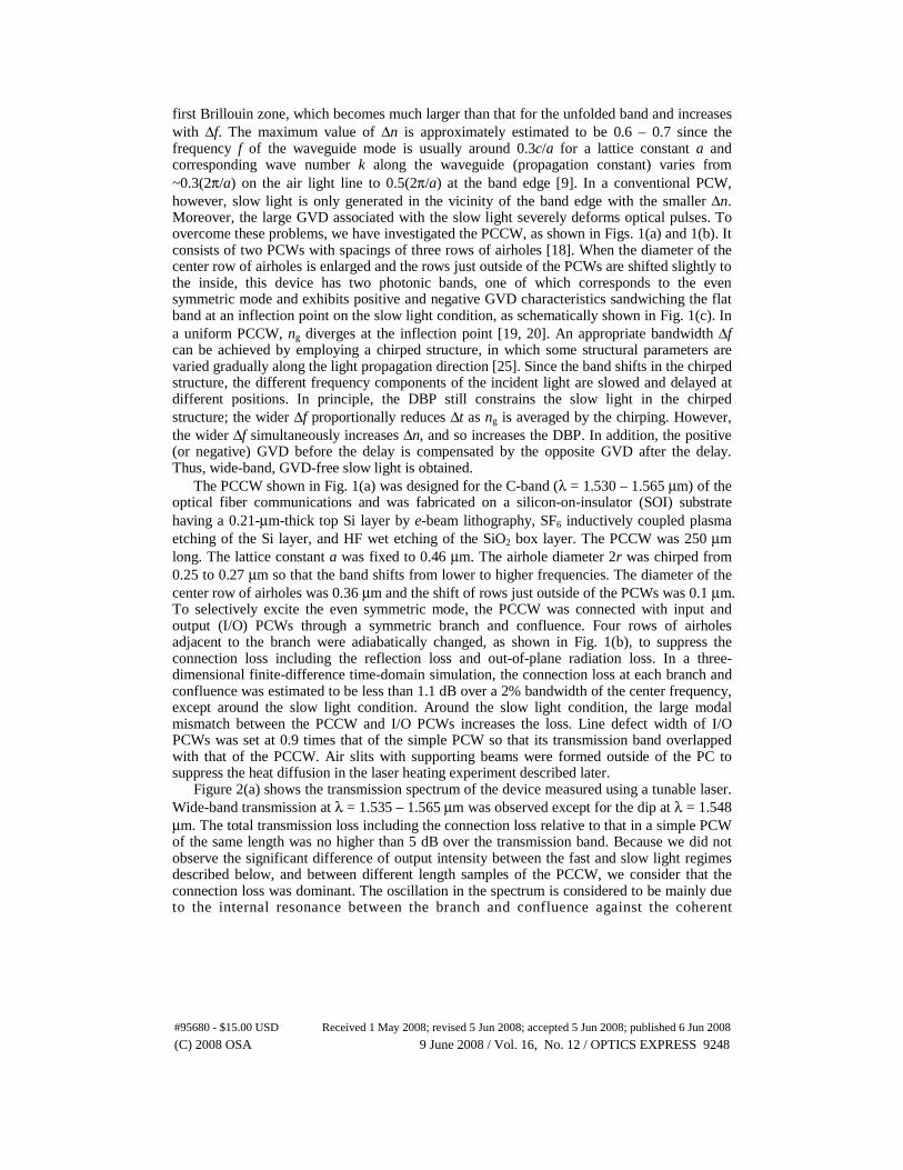
The PCCW shown in Fig. 1(a) was designed for the C-band (λ = 1.530 – 1.565 μm) of the optical fiber communications and was fabricated on a silicon-on-insulator (SOI) substrate having a 0.21-μm-thick top Si layer by e-beam lithography, SF6 inductively coupled plasma etching of the Si layer, and HF wet etching of the SiO2 box layer. The PCCW was 250 μm long. The lattice constant a was fixed to 0.46 μm. The airhole diameter 2r was chirped from 0.25 to 0.27 μm so that the band shifts from lower to higher frequencies. The diameter of the center row of airholes was 0.36 μm and the shift of rows just outside of the PCWs was 0.1 μm. To selectively excite the even symmetric mode, the PCCW was connected with input and output (I/O) PCWs through a symmetric branch and confluence. Four rows of airholes adjacent to the branch were adiabatically changed, as shown in Fig. 1(b), to suppress the connection loss including the reflection loss and out-of-plane radiation loss. In a three-dimensional finite-difference time-domain simulation, the connection loss at each branch and confluence was estimated to be less than 1.1 dB over a 2% bandwidth of the center frequency, except around the slow light condition. Around the slow light condition, the large modal mismatch between the PCCW and I/O PCWs increases the loss. Line defect width of I/O PCWs was set at 0.9 times that of the simple PCW so that its transmission band overlapped with that of the PCCW. Air slits with supporting beams were formed outside of the PC to suppress the heat diffusion in the laser heating experiment described later.
Figure 2(a) shows the transmission spectrum of the device measured using a tunable laser. Wide-band transmission at λ = 1.535 – 1.565 μm was observed except for the dip at λ = 1.548 μm. The total transmission loss including the connection loss relative to that in a simple PCW of the same length was no higher than 5 dB over the transmission band. Because we did not observe the significant difference of output intensity between the fast and slow light regimes described below, and between different length samples of the PCCW, we consider that the connection loss was dominant. The oscillation in the spectrum is considered to be mainly due to the internal resonance between the branch and confluence against the coherent
#95680 - $15.00 USD Received 1 May 2008; revised 5 Jun 2008; accepted 5 Jun 2008; published 6 Jun 2008
(C) 2008 OSA 9 June 2008 / Vol. 16, No. 12 / OPTICS EXPRESS 9248
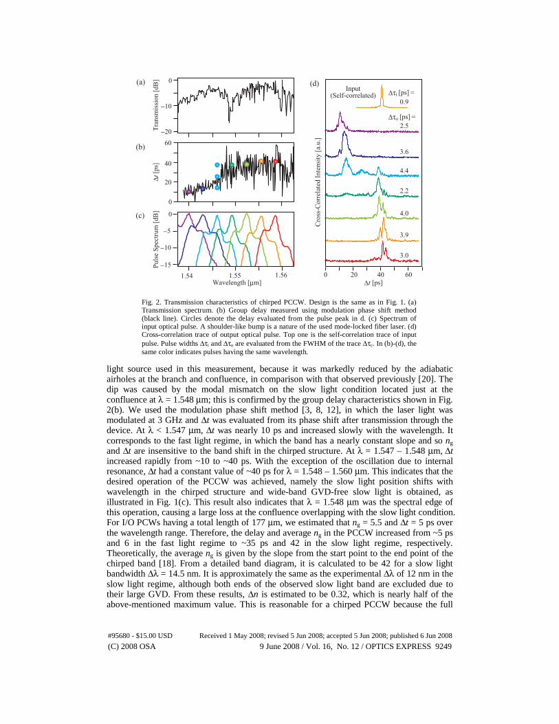
light source used in this measurement, because it was markedly reduced by the adiabatic airholes at the branch and confluence, in comparison with that observed previously [20]. The dip was caused by the modal mismatch on the slow light condition located just at the confluence at λ = 1.548 μm; this is confirmed by the group delay characteristics shown in Fig. 2(b). We used the modulation phase shift method [3, 8, 12], in which the laser light was modulated at 3 GHz and Δt was evaluated from its phase shift after transmission through the device. At λ < 1.547 μm, Δt was nearly 10 ps and increased slowly with the wavelength. It corresponds to the fast light regime, in which the band has a nearly constant slope and so ng and Δt are insensitive to the band shift in the chirped structure. At λ = 1.547 – 1.548 μm, Δt increased rapidly from ~10 to ~40 ps. With the exception of the oscillation due to internal resonance, Δt had a constant value of ~40 ps for λ = 1.548 – 1.560 μm. This indicates that the desired operation of the PCCW was achieved, namely the slow light position shifts with wavelength in the chirped structure and wide-band GVD-free slow light is obtained, as illustrated in Fig. 1(c). This result also indicates that λ = 1.548 μm was the spectral edge of this operation, causing a large loss at the confluence overlapping with the slow light condition. For I/O PCWs having a total length of 177 μm, we estimated that ng = 5.5 and Δt = 5 ps over the wavelength range. Therefore, the delay and average ng in the PCCW increased from ~5 ps and 6 in the fast light regime to ~35 ps and 42 in the slow light regime, respectively. Theoretically, the average ng is given by the slope from the start point to the end point of the chirped band [18]. From a detailed band diagram, it is calculated to be 42 for a slow light bandwidth Δλ = 14.5 nm. It is approximately the same as the experimental Δλ of 12 nm in the slow light regime, although both ends of the observed slow light band are excluded due to their large GVD. From these results, Δn is estimated to be 0.32, which is nearly half of the above-mentioned maximum value. This is reasonable for a chirped PCCW because the full
0
0
20
40
60
1.54 1.561.55
Tran
smis
sion
[dB
]
Cro
ss-C
orre
late
d In
tens
ity [a
.u.]
(a)
(b)
(c)
(d)
0 20 60
2.5
2.2
0.9
3.6
4.4
4.0
3.9
3.0
Input(Self-correlated)
40
0
Puls
e Sp
ectru
m [d
B]
Fig. 2. Transmission characteristics of chirped PCCW. Design is the same as in Fig. 1. (a) Transmission spectrum. (b) Group delay measured using modulation phase shift method (black line). Circles denote the delay evaluated from the pulse peak in d. (c) Spectrum of input optical pulse. A shoulder-like bump is a nature of the used mode-locked fiber laser. (d) Cross-correlation trace of output optical pulse. Top one is the self-correlation trace of input pulse. Pulse widths Δτi and Δτo are evaluated from the FWHM of the trace Δτc. In (b)-(d), the same color indicates pulses having the same wavelength.
#95680 - $15.00 USD Received 1 May 2008; revised 5 Jun 2008; accepted 5 Jun 2008; published 6 Jun 2008
(C) 2008 OSA 9 June 2008 / Vol. 16, No. 12 / OPTICS EXPRESS 9249
bandwidth available below the light line is divided into two regions having the opposite GVD characteristics. The corresponding DBP is 57. Compared with slow light from other sources except for that using a long highly dispersive optical fiber, the present device had the highest DBP and almost the widest Δf. This is attributed to the large Δn for a wide Δf as well as the long device length L. A DBP from several hundreds to about a thousand is expected to be obtainable by increasing L to the order of millimeters.
To evaluate further the wide-band, low GVD operation and its delay, we measured the cross-correlation for short optical pulse transmission. In the modulation phase shift measurement, the internal resonance caused the delay spectrum to oscillate. However, this should not affect the short pulse transmission when the pulse width is much shorter than the round trip time (40 ps × 2 in the in the slow light regime) and the interval between pulses is sufficiently long. We inserted optical pulses from a tunable mode-locked fiber laser into the device with a 25 ns interval. The input pulse width (FWHM) Δτi was evaluated from the self-correlation trace to be 0.9 ps and the corresponding wavelength spectral width was 2 nm at 1/2 intensity and 6 nm at 1/10 intensity, as shown in Fig. 2(c). The cross-correlation trace of the output pulse was taken with a reference pulse of the same width passing through a fiber branch. The results are shown in Fig. 2(d), where the peak wavelength of the pulse λp was tuned every 3.3 nm in the range 1.538 – 1.558 μm (λp of the tunable laser could not be tuned continuously, but rather semi-discretely with this separation). The output pulse was observed over the transmission band. The pulse delay Δt clearly switched from ~10 to ~40 ps at λ ~ 1.547 μm, and Δt was almost constant in the slow light regime. The large splitting of the pulse at λp = 1.546 μm reflects the pulse spectrum overlapped with both the fast and slow light regimes. Circular plots in Fig. 2(b) denote the delay of the pulse peak, showing very good agreement with the modulation phase-shift measurement. Approximating the pulse shape to be Gaussian and using the relation Δτi
2+Δτo2 = Δτc
2 for the pulse width Δτc of the cross-correlation trace, the output pulse width Δτo was evaluated to be 2.2 – 4.4 ps (3.3 ps in an average). The broadening and small splitting of each pulse is not expected to be due to the internal resonance but it might be due to the local GVD in the fabricated chirped structure with some disordering. The short pulse transmission suggests the compensation of most of the GVD of the slow light in the device, while the number of signal bits must be severely counted as 12 by considering the pulse delay and the pulse broadening.
In the second part of this paper, we discuss the tunability of slow light in the PCCW. Thus far, variable ng and Δt have been demonstrated only for the slow light at the band-edge with a large GVD in a simple PCW by shifting the band by heating [5]. Observable time shifts of optical pulses by external control have been unachievable in any on-chip slow light devices. In our chirped PCCW, variable ng is not obtained by a simple band shift since it only shifts the slow light band. Here, we propose to control the slope of the chirping (amount of chirping for a fixed device length L), which simultaneously changes ng and Δλ, as theoretically discussed in ref. [18] and illustrated in Fig. 1(c). (Note that, in the following case, the band shifts in the opposite direction to that in Fig. 1(c)). In the present device, the airhole diameter is chirped. Increasing or decreasing the slab index along the PCCW effectively changes the net slope of the chirping. In this study, local heating of the device by laser irradiation was used, which produced a slope in the slab index due to intensity profile of the laser spot and thermal diffusion. Heating was achieved by focussing blue laser light (λ = 0.442 μm) to an elliptical spot (80 μm × 36 μm, 200 μm × 90 μm, or 400 μm × 180 μm) having a Gaussian-like profile on the PCCW. We estimated the temperature distribution in a sample device, in which a point-defect PC nanocavity was integrated adjacent to the simple PCW. The red shift of the resonance Δλres and the estimated change in the material index of the slab Δnslab increased linearly with the irradiated power P and decreased linearly to semi-exponentially with the distance from the spot center. The distance was elongated with the spot size. To suppress heat diffusion in the lateral directions and increase the heating efficiency, rectangular air slits were formed beside the PC with supporting beams, as shown in Fig. 1(a). The maximum values of
#95680 - $15.00 USD Received 1 May 2008; revised 5 Jun 2008; accepted 5 Jun 2008; published 6 Jun 2008
(C) 2008 OSA 9 June 2008 / Vol. 16, No. 12 / OPTICS EXPRESS 9250
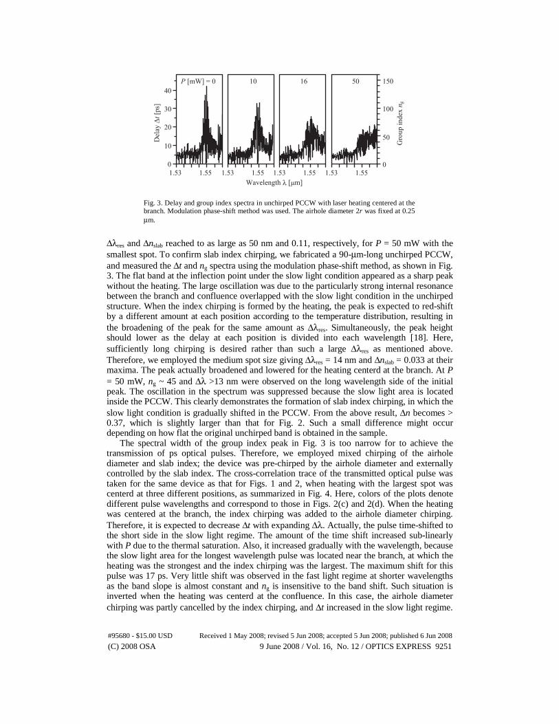
Δλres and Δnslab reached to as large as 50 nm and 0.11, respectively, for P = 50 mW with the smallest spot. To confirm slab index chirping, we fabricated a 90-μm-long unchirped PCCW, and measured the Δt and ng spectra using the modulation phase-shift method, as shown in Fig. 3. The flat band at the inflection point under the slow light condition appeared as a sharp peak without the heating. The large oscillation was due to the particularly strong internal resonance between the branch and confluence overlapped with the slow light condition in the unchirped structure. When the index chirping is formed by the heating, the peak is expected to red-shift by a different amount at each position according to the temperature distribution, resulting in the broadening of the peak for the same amount as Δλres. Simultaneously, the peak height should lower as the delay at each position is divided into each wavelength [18]. Here, sufficiently long chirping is desired rather than such a large Δλres as mentioned above. Therefore, we employed the medium spot size giving Δλres = 14 nm and Δnslab = 0.033 at their maxima. The peak actually broadened and lowered for the heating centerd at the branch. At P = 50 mW, ng ~ 45 and Δλ >13 nm were observed on the long wavelength side of the initial peak. The oscillation in the spectrum was suppressed because the slow light area is located inside the PCCW. This clearly demonstrates the formation of slab index chirping, in which the slow light condition is gradually shifted in the PCCW. From the above result, Δn becomes > 0.37, which is slightly larger than that for Fig. 2. Such a small difference might occur depending on how flat the original unchirped band is obtained in the sample.
The spectral width of the group index peak in Fig. 3 is too narrow for to achieve the transmission of ps optical pulses. Therefore, we employed mixed chirping of the airhole diameter and slab index; the device was pre-chirped by the airhole diameter and externally controlled by the slab index. The cross-correlation trace of the transmitted optical pulse was taken for the same device as that for Figs. 1 and 2, when heating with the largest spot was centerd at three different positions, as summarized in Fig. 4. Here, colors of the plots denote different pulse wavelengths and correspond to those in Figs. 2(c) and 2(d). When the heating was centered at the branch, the index chirping was added to the airhole diameter chirping. Therefore, it is expected to decrease Δt with expanding Δλ. Actually, the pulse time-shifted to the short side in the slow light regime. The amount of the time shift increased sub-linearly with P due to the thermal saturation. Also, it increased gradually with the wavelength, because the slow light area for the longest wavelength pulse was located near the branch, at which the heating was the strongest and the index chirping was the largest. The maximum shift for this pulse was 17 ps. Very little shift was observed in the fast light regime at shorter wavelengths as the band slope is almost constant and ng is insensitive to the band shift. Such situation is inverted when the heating was centerd at the confluence. In this case, the airhole diameter chirping was partly cancelled by the index chirping, and Δt increased in the slow light regime.
40
30
20
10
1.53 1.55 1.53 1.55 1.53 1.55 1.53 1.550
Gro
up in
dex
n g
150
100
50
0
10 16 50P [mW] = 0
Fig. 3. Delay and group index spectra in unchirped PCCW with laser heating centered at the branch. Modulation phase-shift method was used. The airhole diameter 2r was fixed at 0.25 μm.
#95680 - $15.00 USD Received 1 May 2008; revised 5 Jun 2008; accepted 5 Jun 2008; published 6 Jun 2008
(C) 2008 OSA 9 June 2008 / Vol. 16, No. 12 / OPTICS EXPRESS 9251
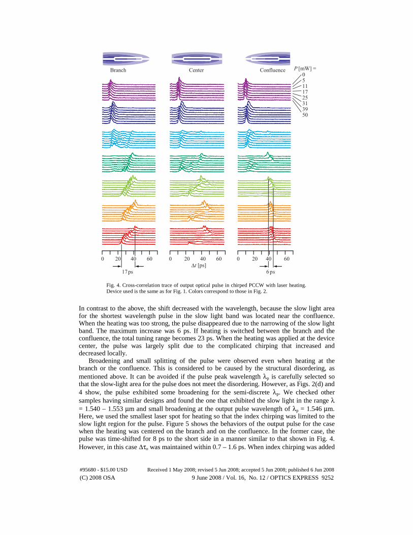
In contrast to the above, the shift decreased with the wavelength, because the slow light area for the shortest wavelength pulse in the slow light band was located near the confluence. When the heating was too strong, the pulse disappeared due to the narrowing of the slow light band. The maximum increase was 6 ps. If heating is switched between the branch and the confluence, the total tuning range becomes 23 ps. When the heating was applied at the device center, the pulse was largely split due to the complicated chirping that increased and decreased locally.
Broadening and small splitting of the pulse were observed even when heating at the branch or the confluence. This is considered to be caused by the structural disordering, as mentioned above. It can be avoided if the pulse peak wavelength λp is carefully selected so that the slow-light area for the pulse does not meet the disordering. However, as Figs. 2(d) and 4 show, the pulse exhibited some broadening for the semi-discrete λp. We checked other samples having similar designs and found the one that exhibited the slow light in the range λ = 1.540 – 1.553 μm and small broadening at the output pulse wavelength of λp = 1.546 μm. Here, we used the smallest laser spot for heating so that the index chirping was limited to the slow light region for the pulse. Figure 5 shows the behaviors of the output pulse for the case when the heating was centered on the branch and on the confluence. In the former case, the pulse was time-shifted for 8 ps to the short side in a manner similar to that shown in Fig. 4. However, in this case Δτo was maintained within 0.7 – 1.6 ps. When index chirping was added
0 20
17ps
60Δt [ps]
0 20 40 60 0 20 60
Branch Center Confluence0
P [mW] =
5111725313950
6 ps
40 40
Fig. 4. Cross-correlation trace of output optical pulse in chirped PCCW with laser heating. Device used is the same as for Fig. 1. Colors correspond to those in Fig. 2.
#95680 - $15.00 USD Received 1 May 2008; revised 5 Jun 2008; accepted 5 Jun 2008; published 6 Jun 2008
(C) 2008 OSA 9 June 2008 / Vol. 16, No. 12 / OPTICS EXPRESS 9252
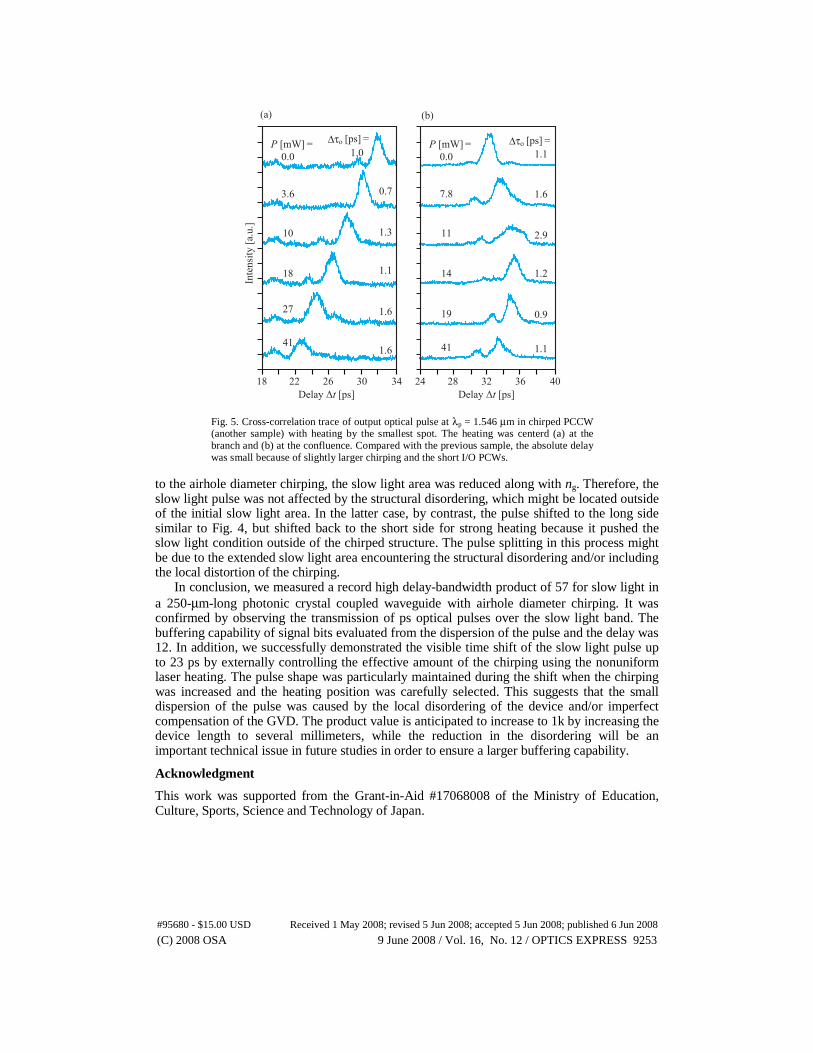
to the airhole diameter chirping, the slow light area was reduced along with ng. Therefore, the slow light pulse was not affected by the structural disordering, which might be located outside of the initial slow light area. In the latter case, by contrast, the pulse shifted to the long side similar to Fig. 4, but shifted back to the short side for strong heating because it pushed the slow light condition outside of the chirped structure. The pulse splitting in this process might be due to the extended slow light area encountering the structural disordering and/or including the local distortion of the chirping.
In conclusion, we measured a record high delay-bandwidth product of 57 for slow light in a 250-μm-long photonic crystal coupled waveguide with airhole diameter chirping. It was confirmed by observing the transmission of ps optical pulses over the slow light band. The buffering capability of signal bits evaluated from the dispersion of the pulse and the delay was 12. In addition, we successfully demonstrated the visible time shift of the slow light pulse up to 23 ps by externally controlling the effective amount of the chirping using the nonuniform laser heating. The pulse shape was particularly maintained during the shift when the chirping was increased and the heating position was carefully selected. This suggests that the small dispersion of the pulse was caused by the local disordering of the device and/or imperfect compensation of the GVD. The product value is anticipated to increase to 1k by increasing the device length to several millimeters, while the reduction in the disordering will be an important technical issue in future studies in order to ensure a larger buffering capability.
Acknowledgment
This work was supported from the Grant-in-Aid #17068008 of the Ministry of Education, Culture, Sports, Science and Technology of Japan.
Inte
nsity
[a.u
.]
3430262218
3.6
0.0
10
18
27
41
P [mW] =
(a) (b)
1.6
1.6
1.1
1.3
0.7
1.0
4036322824
7.8
0.0
11
14
19
41
P [mW] =
1.1
0.9
1.2
2.9
1.6
1.1
Fig. 5. Cross-correlation trace of output optical pulse at λp = 1.546 μm in chirped PCCW (another sample) with heating by the smallest spot. The heating was centerd (a) at the branch and (b) at the confluence. Compared with the previous sample, the absolute delay was small because of slightly larger chirping and the short I/O PCWs.
#95680 - $15.00 USD Received 1 May 2008; revised 5 Jun 2008; accepted 5 Jun 2008; published 6 Jun 2008
(C) 2008 OSA 9 June 2008 / Vol. 16, No. 12 / OPTICS EXPRESS 9253
Recommended