This is information on a product in full production.
November 2017 DocID2470 Rev 12 1/20
LM2903
Low-power dual voltage comparator
Datasheet - production data
Features
Wide single supply voltage range or dual supplies +2 V to +36 V or ±1 V to ±18 V
Very low supply current (0.4 mA) independent of supply voltage (1 mW/comparator at +5 V)
Low input bias current: 25 nA typ.
Low input offset current: ±5 nA typ.
Input common-mode voltage range includes negative rail
Low output saturation voltage:250 mV typ. (IO = 4 mA)
Differential input voltage range equal to the supply voltage
TTL, DTL, ECL, MOS, CMOS compatible outputs
Automotive qualification
Related products
See LM2903W for similar device with higher ESD performances
See LM2903H for similar device with operating temperature up to 150 °C
Description
This device consists of two independent low-power voltage comparators designed specifically to operate from a single supply over a wide range of voltages. Operation from split power supplies is also possible.
In addition, the device has a unique characteristic in that the input common-mode voltage range includes the negative rail even though operated from a single power supply voltage.
www.st.com
Contents LM2903
2/20 DocID2470 Rev 12
Contents
1 Schematic diagram . . . . . . . . . . . . . . . . . . . . . . . . . . . . . . . . . . . . . . . . . . 3
2 Package pin connections . . . . . . . . . . . . . . . . . . . . . . . . . . . . . . . . . . . . . 4
3 Absolute maximum ratings and operating conditions . . . . . . . . . . . . . 5
4 Electrical characteristics . . . . . . . . . . . . . . . . . . . . . . . . . . . . . . . . . . . . . 6
5 Typical application schematics . . . . . . . . . . . . . . . . . . . . . . . . . . . . . . . . 8
6 Package information . . . . . . . . . . . . . . . . . . . . . . . . . . . . . . . . . . . . . . . . 11
6.1 SO8 package information . . . . . . . . . . . . . . . . . . . . . . . . . . . . . . . . . . . . . 12
6.2 TSSOP8 package information . . . . . . . . . . . . . . . . . . . . . . . . . . . . . . . . . 13
6.3 MiniSO8 package information . . . . . . . . . . . . . . . . . . . . . . . . . . . . . . . . . 14
6.4 DFN8 2x2 package mechanical data (LM2903Q2T) . . . . . . . . . . . . . . . . 15
6.5 DFN8 2x2 package mechanical data (LM2903YQ3T) . . . . . . . . . . . . . . . 17
7 Ordering information . . . . . . . . . . . . . . . . . . . . . . . . . . . . . . . . . . . . . . . 18
8 Revision history . . . . . . . . . . . . . . . . . . . . . . . . . . . . . . . . . . . . . . . . . . . 19
DocID2470 Rev 12 3/20
LM2903 Schematic diagram
20
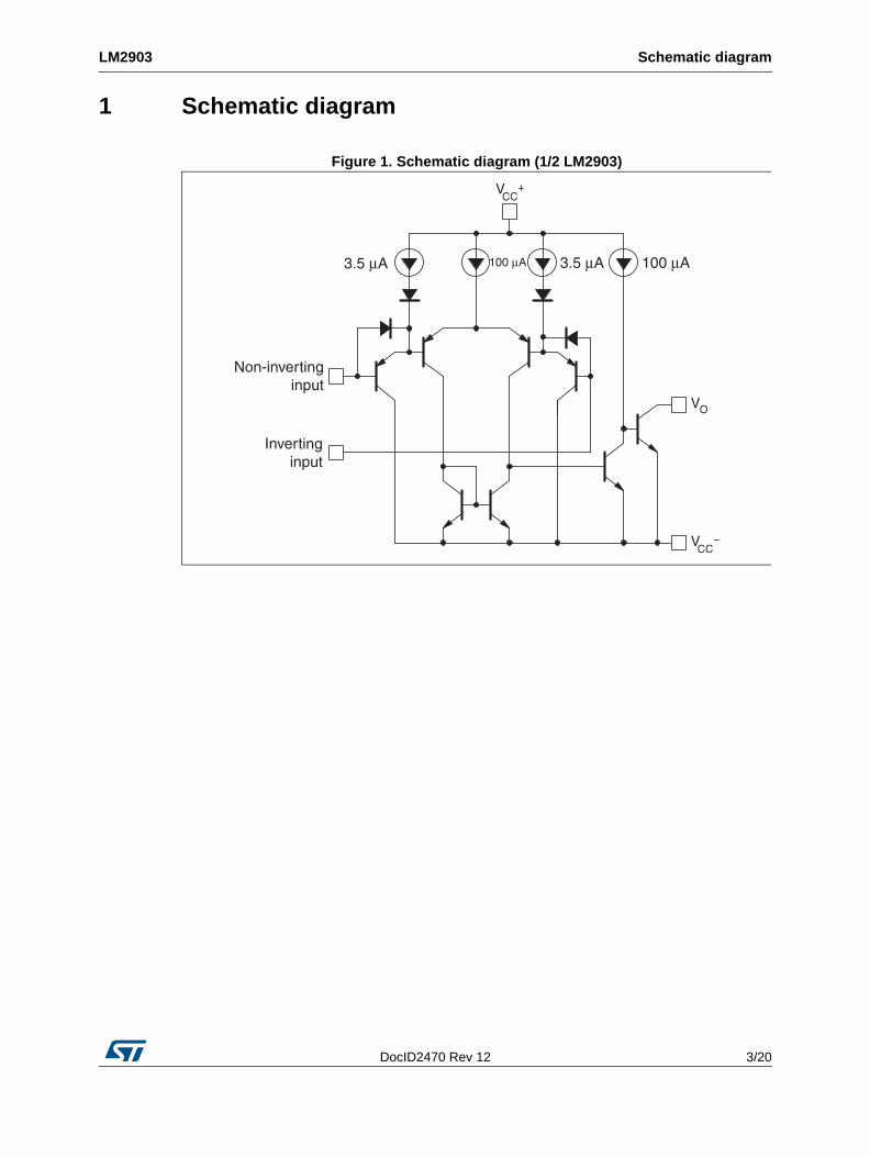
1 Schematic diagram
Figure 1. Schematic diagram (1/2 LM2903)
3.5 μA 100 μA 3.5 μA 100 μA
Non-invertinginput
Invertinginput
Package pin connections LM2903
4/20 DocID2470 Rev 12
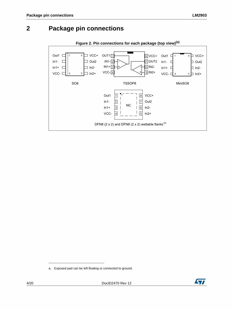
2 Package pin connections
Figure 2. Pin connections for each package (top view)(a)
a. Exposed pad can be left floating or connected to ground.
DocID2470 Rev 12 5/20
LM2903 Absolute maximum ratings and operating conditions
20
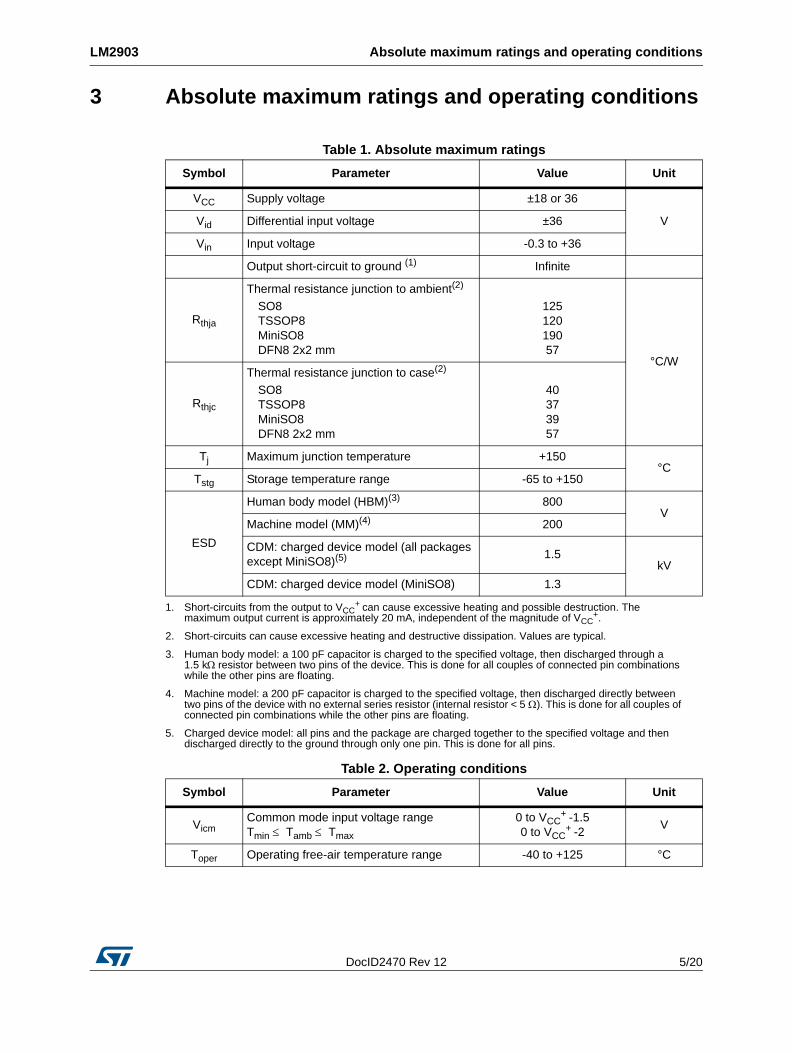
3 Absolute maximum ratings and operating conditions
Table 1. Absolute maximum ratings
Symbol Parameter Value Unit
VCC Supply voltage ±18 or 36
VVid Differential input voltage ±36
Vin Input voltage -0.3 to +36
Output short-circuit to ground (1)
1. Short-circuits from the output to VCC+ can cause excessive heating and possible destruction. The
maximum output current is approximately 20 mA, independent of the magnitude of VCC+.
Infinite
Rthja
Thermal resistance junction to ambient(2)
SO8 TSSOP8MiniSO8DFN8 2x2 mm
2. Short-circuits can cause excessive heating and destructive dissipation. Values are typical.
12512019057
°C/W
Rthjc
Thermal resistance junction to case(2)
SO8 TSSOP8MiniSO8DFN8 2x2 mm
40373957
Tj Maximum junction temperature +150°C
Tstg Storage temperature range -65 to +150
ESD
Human body model (HBM)(3)
3. Human body model: a 100 pF capacitor is charged to the specified voltage, then discharged through a 1.5 kresistor between two pins of the device. This is done for all couples of connected pin combinations while the other pins are floating.
800V
Machine model (MM)(4)
4. Machine model: a 200 pF capacitor is charged to the specified voltage, then discharged directly between two pins of the device with no external series resistor (internal resistor < 5 ). This is done for all couples of connected pin combinations while the other pins are floating.
200
CDM: charged device model (all packages except MiniSO8)(5)
5. Charged device model: all pins and the package are charged together to the specified voltage and then discharged directly to the ground through only one pin. This is done for all pins.
1.5kV
CDM: charged device model (MiniSO8) 1.3
Table 2. Operating conditions
Symbol Parameter Value Unit
VicmCommon mode input voltage rangeTmin Tamb Tmax
0 to VCC+ -1.5
0 to VCC+ -2
V
Toper Operating free-air temperature range -40 to +125 °C
Electrical characteristics LM2903
6/20 DocID2470 Rev 12
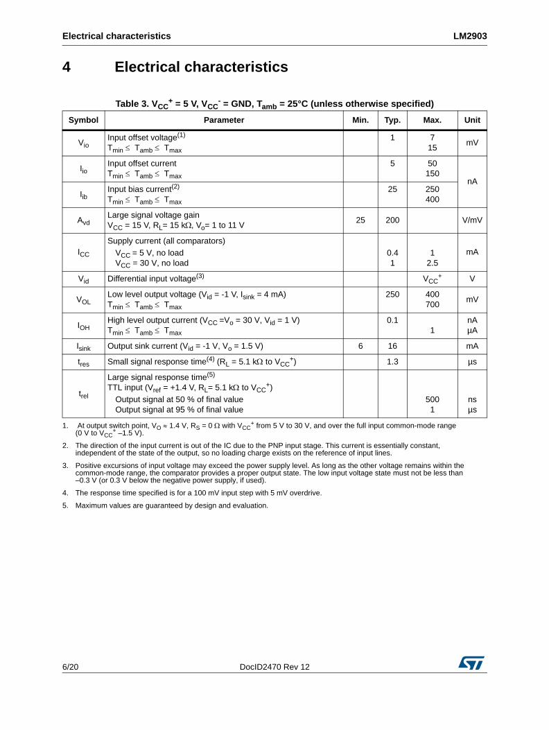
4 Electrical characteristics
Table 3. VCC+ = 5 V, VCC
- = GND, Tamb = 25°C (unless otherwise specified)
Symbol Parameter Min. Typ. Max. Unit
VioInput offset voltage(1) Tmin Tamb Tmax
1 715
mV
IioInput offset current Tmin Tamb Tmax
5 50150
nA
IibInput bias current(2)Tmin Tamb Tmax
25 250400
AvdLarge signal voltage gainVCC = 15 V, RL= 15 k, Vo= 1 to 11 V
25 200 V/mV
ICC
Supply current (all comparators)
VCC = 5 V, no loadVCC = 30 V, no load
0.41
12.5
mA
Vid Differential input voltage(3) VCC+ V
VOLLow level output voltage (Vid = -1 V, Isink = 4 mA)Tmin Tamb Tmax
250 400700
mV
IOHHigh level output current (VCC =Vo = 30 V, Vid = 1 V)Tmin Tamb Tmax
0.11
nAµA
Isink Output sink current (Vid = -1 V, Vo = 1.5 V) 6 16 mA
tres Small signal response time(4) (RL = 5.1 k to VCC+) 1.3 µs
trel
Large signal response time(5)TTL input (Vref = +1.4 V, RL= 5.1 k to VCC
+)
Output signal at 50 % of final valueOutput signal at 95 % of final value
5001
nsµs
1. At output switch point, VO 1.4 V, RS = 0 with VCC+ from 5 V to 30 V, and over the full input common-mode range
(0 V to VCC+ –1.5 V).
2. The direction of the input current is out of the IC due to the PNP input stage. This current is essentially constant, independent of the state of the output, so no loading charge exists on the reference of input lines.
3. Positive excursions of input voltage may exceed the power supply level. As long as the other voltage remains within the common-mode range, the comparator provides a proper output state. The low input voltage state must not be less than –0.3 V (or 0.3 V below the negative power supply, if used).
4. The response time specified is for a 100 mV input step with 5 mV overdrive.
5. Maximum values are guaranteed by design and evaluation.
DocID2470 Rev 12 7/20
LM2903 Electrical characteristics
20
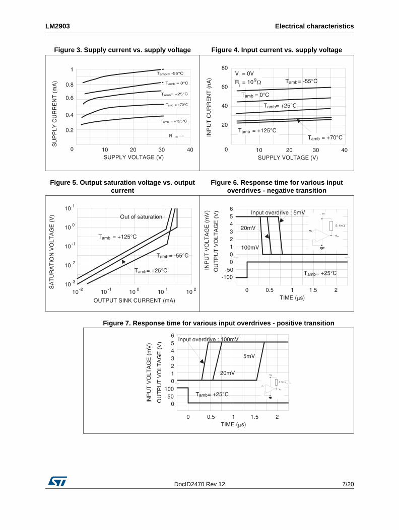
Figure 7. Response time for various input overdrives - positive transition
Figure 3. Supply current vs. supply voltage Figure 4. Input current vs. supply voltage
Figure 5. Output saturation voltage vs. output current
Figure 6. Response time for various input overdrives - negative transition
Typical application schematics LM2903
8/20 DocID2470 Rev 12
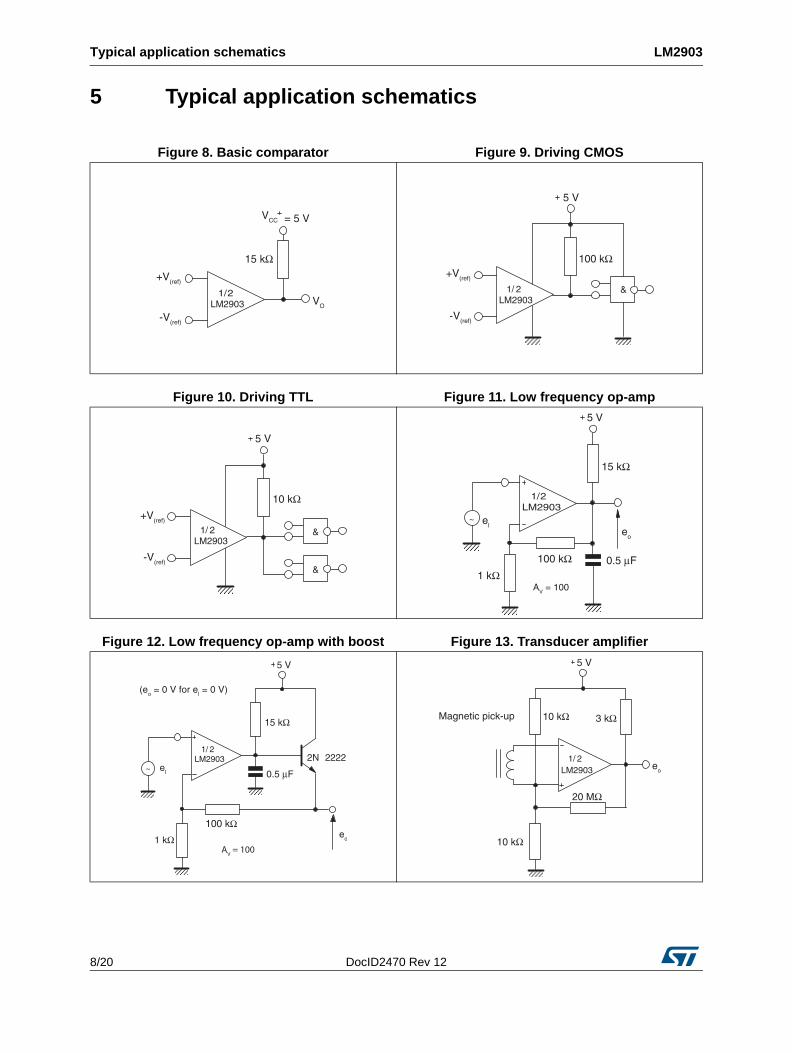
5 Typical application schematics
Figure 8. Basic comparator Figure 9. Driving CMOS
VCC = 5 V
15 kΩ
VO
+V(ref)
1/2LM2903
-V(ref)
5 V
100 kΩ
&1/ 2LM2903
+V(ref)
-V(ref)
Figure 10. Driving TTL Figure 11. Low frequency op-amp
5 V
10 kΩ+V(ref)
&
&
1/ 2LM2903
-V(ref)
5 V
15 kΩ
eo
0.5 μF100 kΩ
el
1 kΩ
~
1/2LM2903
AV = 100
Figure 12. Low frequency op-amp with boost Figure 13. Transducer amplifier
5 V
15 kΩ
0.5 μF
100 kΩ
1 kΩ
~2N 2222
(eo = 0 V for el = 0 V)
1/ 2LM2903
eo
el
AV = 100
5 V
10 kΩ
eo
20 MΩ
3 kΩ Magnetic pick-up
10 kΩ
1/ 2LM2903
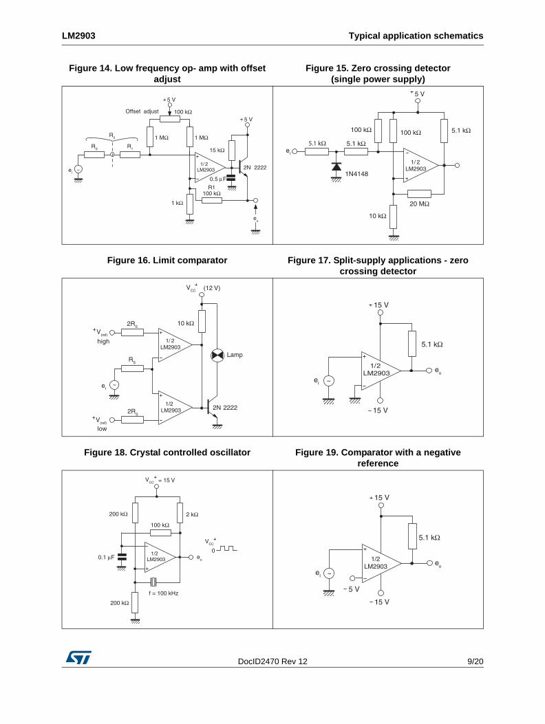
DocID2470 Rev 12 9/20
LM2903 Typical application schematics
20
Figure 14. Low frequency op- amp with offset adjust
Figure 15. Zero crossing detector (single power supply)
el~ 2N 2222
5 V
eo
R1100 kΩ
1 kΩ
5 V
1 MΩ
100 kΩ
1 MΩ
Offset adjust
RS R1 15 kΩ
0.5 μF
R2
1/ 2LM2903
100 kΩ
10 kΩ
el
20 MΩ
5 V
1N4148
5.1 kΩ
5.1 kΩ100 kΩ
1/ 2LM2903
5.1 kΩ
Figure 16. Limit comparator Figure 17. Split-supply applications - zero crossing detector
10 kΩ
eI~
RS
2RS
V(ref)
high
V(ref)
low
2N 2222
VCC
Lamp
1/ 2LM2903
1/2LM29032RS
(12 V)
15 V
5.1 kΩ
eo
eI ~
15 V
1/2LM2903
Figure 18. Crystal controlled oscillator Figure 19. Comparator with a negative reference
2 kΩ
200 kΩ
eo
VCC
0
100 kΩ
200 kΩ
1/2LM29030.1 μF
f = 100 kHz
VCC = 15 V
15 V
5.1 kΩ
eo
eI ~
15 V
5 V
1/2LM2903
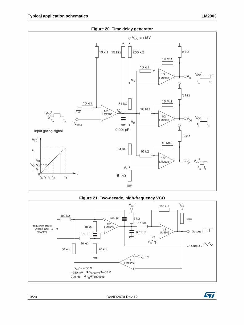
Typical application schematics LM2903
10/20 DocID2470 Rev 12
Figure 20. Time delay generator
Figure 21. Two-decade, high-frequency VCO
VCC0
V(ref.)
10 kΩ
1/2
15 kΩ 200 kΩ 3 kΩ
3 kΩ
3 kΩ
10 MΩ
VO2
V03
O1V
51 kΩ
V1
V2
0.001μF
VC1
V3
VCC
VC1
V1
V2
V3
00 1t t 3t 4t2t
t
VCC
t0
t1
VCC
VCC
VCC = +15V
1/2LM2903
1/2
1/2
10 kΩ
10 kΩ
10 kΩ
10 kΩ
10 MΩ
10 MΩ
51 kΩ
51 kΩ
t2
to
t3
to
tA
to
Input gating signal
LM2903
LM2903
LM2903
VCC VCC100 kΩ
3 kΩ5.1 kΩ
/2
VCC /2
0.01 μF
500 pF100 kΩ
0.1 μF
20 kΩ
50 kΩ
= + 30 V
+250 mV Vcontrol +50 V
700 Hz f 100 kHzo
20 kΩ
3 kΩ
1/ 2LM2903
1/ 2LM2903
1/ 2LM2903
Output 1
Output 2
VCC
VCC
Frequency controlvoltage input
Vcontrol
10 kΩ
DocID2470 Rev 12 11/20
LM2903 Package information
20
6 Package information
In order to meet environmental requirements, ST offers these devices in different grades of ECOPACK® packages, depending on their level of environmental compliance. ECOPACK® specifications, grade definitions and product status are available at: www.st.com. ECOPACK® is an ST trademark.
Package information LM2903
12/20 DocID2470 Rev 12
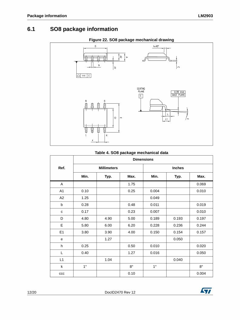
6.1 SO8 package information
Figure 22. SO8 package mechanical drawing
Table 4. SO8 package mechanical data
Ref.
Dimensions
Millimeters Inches
Min. Typ. Max. Min. Typ. Max.
A 1.75 0.069
A1 0.10 0.25 0.004 0.010
A2 1.25 0.049
b 0.28 0.48 0.011 0.019
c 0.17 0.23 0.007 0.010
D 4.80 4.90 5.00 0.189 0.193 0.197
E 5.80 6.00 6.20 0.228 0.236 0.244
E1 3.80 3.90 4.00 0.150 0.154 0.157
e 1.27 0.050
h 0.25 0.50 0.010 0.020
L 0.40 1.27 0.016 0.050
L1 1.04 0.040
k 1° 8° 1° 8°
ccc 0.10 0.004
DocID2470 Rev 12 13/20
LM2903 Package information
20
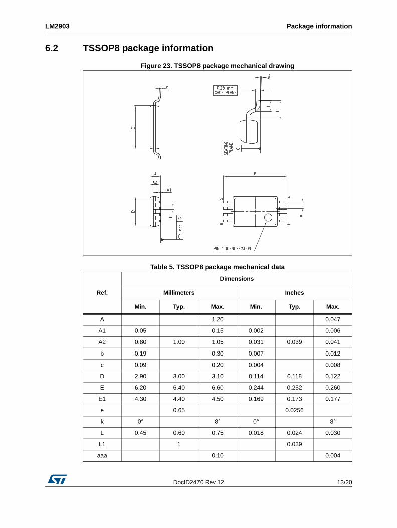
6.2 TSSOP8 package information
Figure 23. TSSOP8 package mechanical drawing
Table 5. TSSOP8 package mechanical data
Ref.
Dimensions
Millimeters Inches
Min. Typ. Max. Min. Typ. Max.
A 1.20 0.047
A1 0.05 0.15 0.002 0.006
A2 0.80 1.00 1.05 0.031 0.039 0.041
b 0.19 0.30 0.007 0.012
c 0.09 0.20 0.004 0.008
D 2.90 3.00 3.10 0.114 0.118 0.122
E 6.20 6.40 6.60 0.244 0.252 0.260
E1 4.30 4.40 4.50 0.169 0.173 0.177
e 0.65 0.0256
k 0° 8° 0° 8°
L 0.45 0.60 0.75 0.018 0.024 0.030
L1 1 0.039
aaa 0.10 0.004
Package information LM2903
14/20 DocID2470 Rev 12
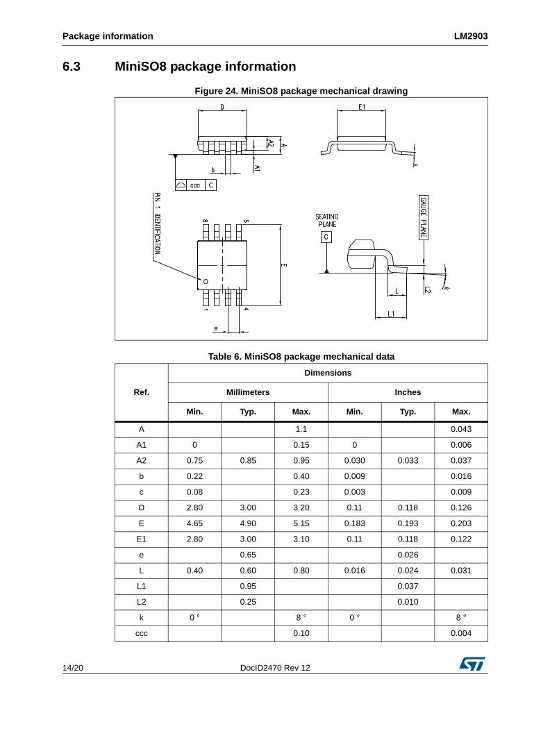
6.3 MiniSO8 package information
Figure 24. MiniSO8 package mechanical drawing
Table 6. MiniSO8 package mechanical data
Ref.
Dimensions
Millimeters Inches
Min. Typ. Max. Min. Typ. Max.
A 1.1 0.043
A1 0 0.15 0 0.006
A2 0.75 0.85 0.95 0.030 0.033 0.037
b 0.22 0.40 0.009 0.016
c 0.08 0.23 0.003 0.009
D 2.80 3.00 3.20 0.11 0.118 0.126
E 4.65 4.90 5.15 0.183 0.193 0.203
E1 2.80 3.00 3.10 0.11 0.118 0.122
e 0.65 0.026
L 0.40 0.60 0.80 0.016 0.024 0.031
L1 0.95 0.037
L2 0.25 0.010
k 0 ° 8 ° 0 ° 8 °
ccc 0.10 0.004
DocID2470 Rev 12 15/20
LM2903 Package information
20
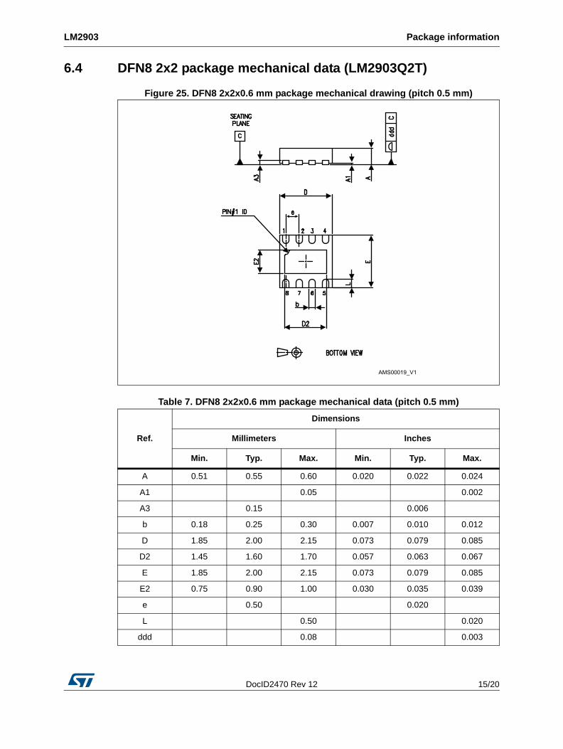
6.4 DFN8 2x2 package mechanical data (LM2903Q2T)
Figure 25. DFN8 2x2x0.6 mm package mechanical drawing (pitch 0.5 mm)
Table 7. DFN8 2x2x0.6 mm package mechanical data (pitch 0.5 mm)
Ref.
Dimensions
Millimeters Inches
Min. Typ. Max. Min. Typ. Max.
A 0.51 0.55 0.60 0.020 0.022 0.024
A1 0.05 0.002
A3 0.15 0.006
b 0.18 0.25 0.30 0.007 0.010 0.012
D 1.85 2.00 2.15 0.073 0.079 0.085
D2 1.45 1.60 1.70 0.057 0.063 0.067
E 1.85 2.00 2.15 0.073 0.079 0.085
E2 0.75 0.90 1.00 0.030 0.035 0.039
e 0.50 0.020
L 0.50 0.020
ddd 0.08 0.003
Package information LM2903
16/20 DocID2470 Rev 12
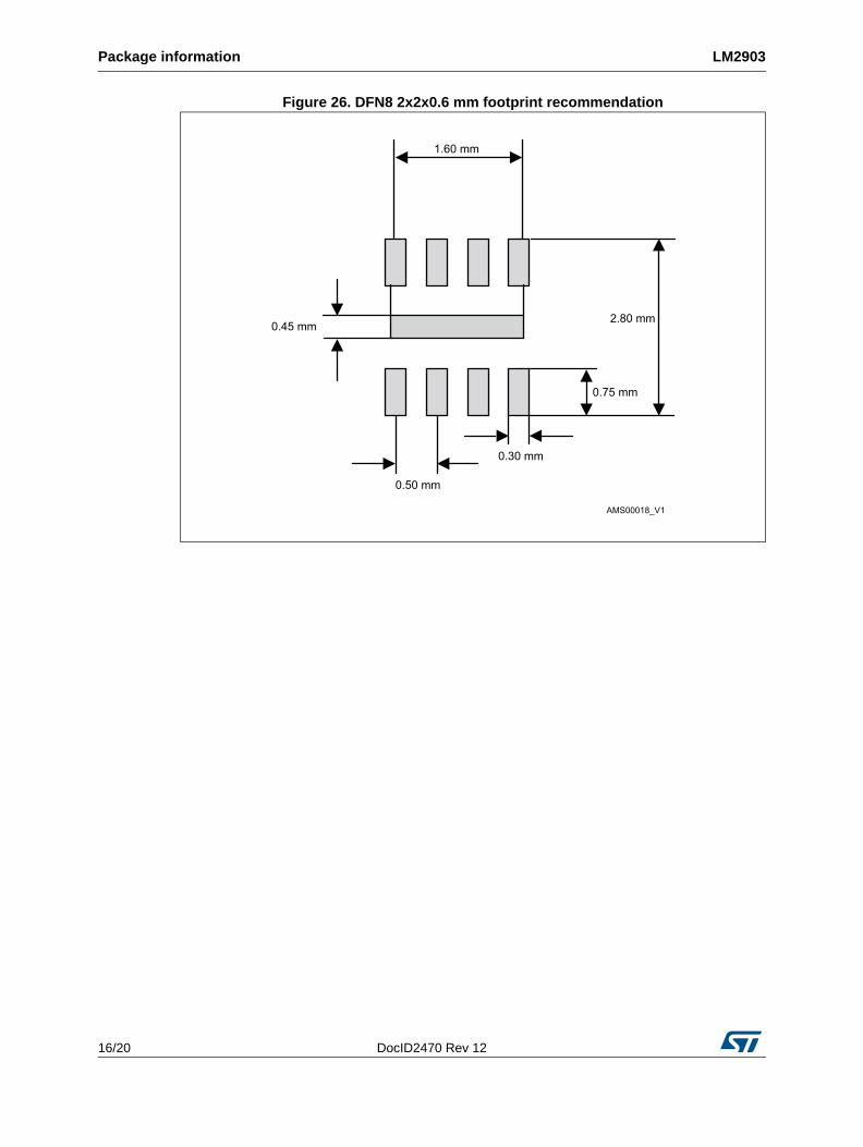
Figure 26. DFN8 2x2x0.6 mm footprint recommendation
DocID2470 Rev 12 17/20
LM2903 Package information
20
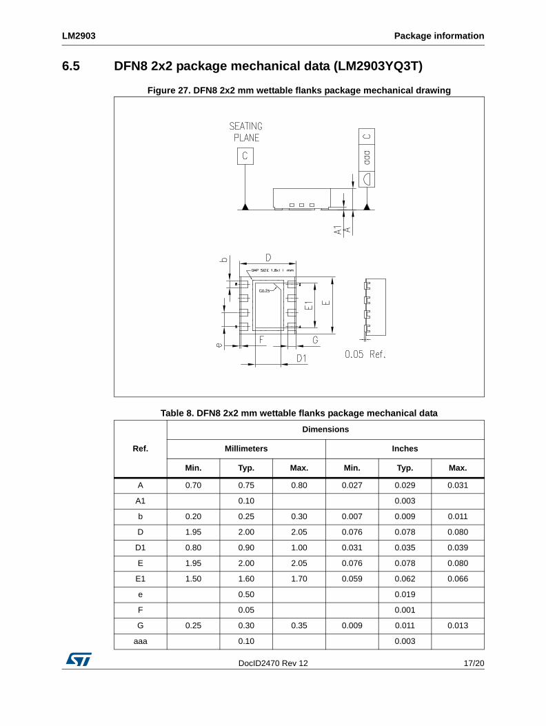
6.5 DFN8 2x2 package mechanical data (LM2903YQ3T)
Figure 27. DFN8 2x2 mm wettable flanks package mechanical drawing
Table 8. DFN8 2x2 mm wettable flanks package mechanical data
Ref.
Dimensions
Millimeters Inches
Min. Typ. Max. Min. Typ. Max.
A 0.70 0.75 0.80 0.027 0.029 0.031
A1 0.10 0.003
b 0.20 0.25 0.30 0.007 0.009 0.011
D 1.95 2.00 2.05 0.076 0.078 0.080
D1 0.80 0.90 1.00 0.031 0.035 0.039
E 1.95 2.00 2.05 0.076 0.078 0.080
E1 1.50 1.60 1.70 0.059 0.062 0.066
e 0.50 0.019
F 0.05 0.001
G 0.25 0.30 0.35 0.009 0.011 0.013
aaa 0.10 0.003
Ordering information LM2903
18/20 DocID2470 Rev 12
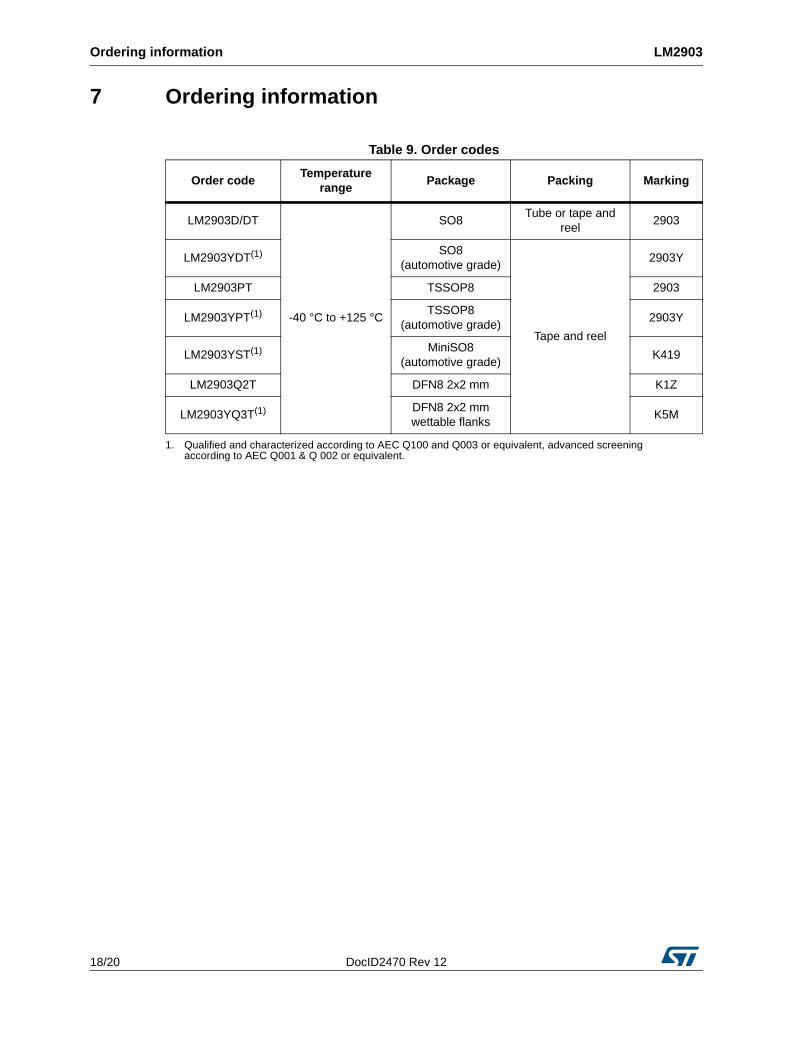
7 Ordering information
Table 9. Order codes
Order codeTemperature
rangePackage Packing Marking
LM2903D/DT
-40 °C to +125 °C
SO8Tube or tape and
reel2903
LM2903YDT(1)
1. Qualified and characterized according to AEC Q100 and Q003 or equivalent, advanced screening according to AEC Q001 & Q 002 or equivalent.
SO8(automotive grade)
Tape and reel
2903Y
LM2903PT TSSOP8 2903
LM2903YPT(1) TSSOP8(automotive grade)
2903Y
LM2903YST(1) MiniSO8(automotive grade)
K419
LM2903Q2T DFN8 2x2 mm K1Z
LM2903YQ3T(1) DFN8 2x2 mm wettable flanks
K5M
DocID2470 Rev 12 19/20
LM2903 Revision history
20
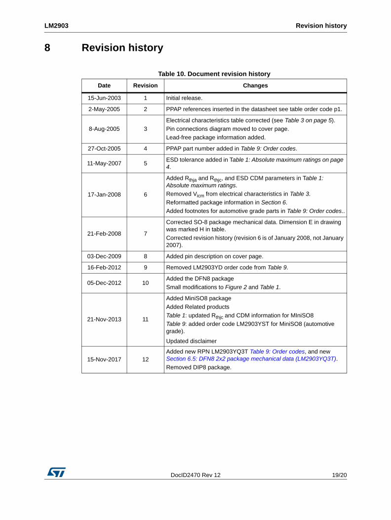
8 Revision history
Table 10. Document revision history
Date Revision Changes
15-Jun-2003 1 Initial release.
2-May-2005 2 PPAP references inserted in the datasheet see table order code p1.
8-Aug-2005 3
Electrical characteristics table corrected (see Table 3 on page 5).
Pin connections diagram moved to cover page.
Lead-free package information added.
27-Oct-2005 4 PPAP part number added in Table 9: Order codes.
11-May-2007 5ESD tolerance added in Table 1: Absolute maximum ratings on page 4.
17-Jan-2008 6
Added Rthja and Rthjc, and ESD CDM parameters in Table 1: Absolute maximum ratings.
Removed Vicm from electrical characteristics in Table 3.
Reformatted package information in Section 6.
Added footnotes for automotive grade parts in Table 9: Order codes..
21-Feb-2008 7
Corrected SO-8 package mechanical data. Dimension E in drawing was marked H in table.
Corrected revision history (revision 6 is of January 2008, not January 2007).
03-Dec-2009 8 Added pin description on cover page.
16-Feb-2012 9 Removed LM2903YD order code from Table 9.
05-Dec-2012 10Added the DFN8 package
Small modifications to Figure 2 and Table 1.
21-Nov-2013 11
Added MiniSO8 package
Added Related products
Table 1: updated Rthjc and CDM information for MIniSO8
Table 9: added order code LM2903YST for MiniSO8 (automotive grade).
Updated disclaimer
15-Nov-2017 12Added new RPN LM2903YQ3T Table 9: Order codes, and new Section 6.5: DFN8 2x2 package mechanical data (LM2903YQ3T).
Removed DIP8 package.
LM2903
20/20 DocID2470 Rev 12
IMPORTANT NOTICE – PLEASE READ CAREFULLY
STMicroelectronics NV and its subsidiaries (“ST”) reserve the right to make changes, corrections, enhancements, modifications, and improvements to ST products and/or to this document at any time without notice. Purchasers should obtain the latest relevant information on ST products before placing orders. ST products are sold pursuant to ST’s terms and conditions of sale in place at the time of order acknowledgement.
Purchasers are solely responsible for the choice, selection, and use of ST products and ST assumes no liability for application assistance or the design of Purchasers’ products.
No license, express or implied, to any intellectual property right is granted by ST herein.
Resale of ST products with provisions different from the information set forth herein shall void any warranty granted by ST for such product.
ST and the ST logo are trademarks of ST. All other product or service names are the property of their respective owners.
Information in this document supersedes and replaces information previously supplied in any prior versions of this document.
© 2017 STMicroelectronics – All rights reserved
Recommended