2017 Microchip Technology Inc. DS20005748A-page 1
MIC2230
Features• High Efficiency: Over 96%• Ultra-Low Quiescent Current: Only 28 μA• Ultra-Low Shutdown Current: Less Than 1 μA• Fast Transient Performance• 2.5 MHz PWM Operation• High Output Current Capability per Channel:
800 mA• No Schottky Diodes Required• Stable with 2.2 μH Inductor, 10 μF Ceramic
Capacitor• Adjustable Output Voltage Down to 0.8V• Built-In Soft-Start Circuitry• Current-Limit Protection• Automatic Switching into Light Load Mode
Operation• /FPWM Pin allows Low-Noise Forced PWM Mode
Operation• Power Good Output with Internal 5 μA Current
Source allows Sequencing with Programmable Delay Time
• Small Thermally Enhanced 3 mm × 3 mm TDFN-12L Package
Applications• MPU & ASIC Power• PDAs• Digital Cameras• PC Cards• Wireless and DSL Modems
General DescriptionThe MIC2230 is a dual output, high-efficiencysynchronous step-down DC/DC converter. TheMIC2230 is ideally suited for portable and embeddedsystems that demand high power conversionefficiencies and fast transient performance, whileoffered in a very small package. The MIC2230 offers anultra-low quiescent current in light load mode, assuringminimum current draw from battery poweredapplications in standby modes. The MIC2230 wasdesigned to only require miniature 2.2 μH inductorsand 10 μF ceramic capacitors.
The MIC2230 features a selectable mode that allowsthe user to trade-off lowest noise performance for lowpower efficiency. Trickle mode operation providesultra-high efficiency at light loads, while PWM operationprovides very low ripple noise performance. Tomaximize battery life in low-dropout conditions,MIC2230 can operate with a maximum duty cycle of100%.
The MIC2230 is available in a space-saving3 mm × 3 mm TDFN-12L package with a junctiontemperature range from –40°C to +125°C.
Package TypesMIC2230
3x3 TDFN* (Fixed)Top View
AGND SW15
1OUT2
EN2
AVIN
SW2
12 OUT1
EN1
PGOOD
VIN
11
10
9
2
3
4
8
PGND /FPWM6 7
MIC22303x3 TDFN* (Adjustable)
Top View
AGND SW15
1FB2
EN2
AVIN
SW2
12 FB1
EN1
PGOOD
VIN
11
10
9
2
3
4
8
PGND /FPWM6 7
Dual Synchronous 800 mA/800 mA Step-Down DC/DC Regulator
MIC2230
DS20005748A-page 2 2017 Microchip Technology Inc.
Typical Application Circuit
Functional Block Diagram
MIC22303x3 TDFN
EN2
SW2
PGND
OUT2
PGOOD
VIN
2.5V to 5.5V
10μF
10μF
VOUT1
1.8V / 800mA
EN1
MIC2230/FPWM
SW1
OUT1
2.2μH
VINAVIN
AGND
10μF
390pF
2.2μH VOUT2
1.575V / 800mA
ON
OFF
ON
OFF
Compensation
Trickle Mode
Logic
Anti
Shoot-through
Logic
HSD
LSD
Anti
Shoot-through
Logic
HSD
LSD
ENABLE
LOGIC
VIN
EN1
SW1
PGOOD
FB1
PGND AGND
FB2
/FPWM
SW2
EN2
AVIN
ISENSE2ISENSE1
AVIN
EA1 EA2
5μA
0.8V 0.8V
1kΩ

2017 Microchip Technology Inc. DS20005748A-page 3
MIC22301.0 ELECTRICAL CHARACTERISTICS
Absolute Maximum Ratings †Supply Voltage, (VIN) ................................................................................................................................................. +6VEnable 1 Voltage........................................................................................................................................................ +6VEnable 2 Voltage........................................................................................................................................................ +6VLogic Input Voltage, (VEN, VFPWM)..................................................................................................................... 0V to VINESD Protection.........................................................................................................................................................+2 kV
Operating Ratings ††Supply Voltage, VIN..................................................................................................................................... +2.5V to 5.5V
† Notice: Exceeding the absolute maximum rating may damage the device.†† Notice: The device is not guaranteed to function outside its operating rating.
DC CHARACTERISTICS (Note 1) Electrical Characteristics: Unless otherwise indicated, TA = 25°C with VIN = VEN1 = VEN2 = 3.6V, VOUT1, VOUT2: L = 2.2 μH, C = 10 μF. Bold values indicate –40ºC TJ +125ºC.
Parameters Sym. Min. Typ. Max. Units Conditions
Supply Voltage and Current
Supply Voltage Range 2.5 — 5.5 V —
UVLO (Rising) 2.3 2.4 2.5 V —
UVLO Hysteresis — 100 — mV —
PWM Mode Supply Current — 560 950 μA
/FPWM = Low; VOUT1,VOUT2 = 1.03 * VNOM (not switching)
Trickle Mode Supply Current — 28 50 μA
/FPWM = High; VOUT1,VOUT2 = 1.03 * VNOM (not switching)
Shutdown Quiescent Current — 0.1 1 μA VEN = 0V
Output Voltage Accuracy
Feedback Voltage, VFB 0.780 0.8 0.820 V Adjustable
Output Voltage, VOUT –2.5 — +2.5 % Fixed Output Options
Feedback Bias Current — 10 — nA —
Output Voltage Line Regulation — 0.1 0.5 % 2.5V VIN 5.5V
Output Voltage Load Regulation — 0.5 — %
VIN = 5V, IOUT = 10 mA to 800 mA, /FPWM = 0VVIN = 3V; IOUT = 10 mA to 800 mA, /FPWM = 0V
Ripple in Trickle Mode — 40 — mV VIN=3.6V; IOUT = 1 mA; COUT = 10 μF, L = 2.2 μH.
Note 1: Specification for packaged product only.

MIC2230
DS20005748A-page 4 2017 Microchip Technology Inc.
Logic Inputs
EN Input Threshold — 0.8 1.2 V On
0.3 0.7 — V Off
EN Input Current — 0.01 1 μA —
/FPWM Input Threshold — — 0.6×VIN V On
0.3×VIN — — V Off
/FPWM Input Current — 0.01 1 μA —
Protection
Current-Limit 0.9 1.2 1.8 A —
Control
Maximum Duty Cycle 100 — — % —
Oscillator
PWM Mode Frequency 2.125 2.5 2.875 MHz —
Power Good
Power Good Reset Threshold
— 6.25 12 % Upper Threshold–14 –8.5 — % Lower Threshold
PGOOD Series Resistance — 1 1.4 kΩ —
PGOOD Pull-Up Current — 5 — μA Output within 8.5% of regulation
Power Switch
Switch On-Resistance— 0.4 — Ω ISW = 150 mA (PFET)
— 0.35 — Ω ISW = 150 mA (NFET)
DC CHARACTERISTICS (Note 1) (CONTINUED)Electrical Characteristics: Unless otherwise indicated, TA = 25°C with VIN = VEN1 = VEN2 = 3.6V, VOUT1, VOUT2: L = 2.2 μH, C = 10 μF. Bold values indicate –40ºC TJ +125ºC.
Parameters Sym. Min. Typ. Max. Units Conditions
Note 1: Specification for packaged product only.

2017 Microchip Technology Inc. DS20005748A-page 5
MIC2230
TEMPERATURE SPECIFICATIONS (Note 1)Parameters Sym. Min. Typ. Max. Units Conditions
Temperature RangesStorage Temperature Range TA –65 — +150 °C —Junction Operating Temperature TJ –40 — +125 °C —Package Thermal Resistances
Thermal Resistance, 3 x 3 QFN-12LdJA — 60 — °C/W —JC — 15 — °C/W —
Note 1: The maximum allowable power dissipation is a function of ambient temperature, the maximum allowable junction temperature and the thermal resistance from junction to air (i.e., TA, TJ, JA). Exceeding the maximum allowable power dissipation will cause the device operating junction temperature to exceed the maximum +125°C rating. Sustained junction temperatures above +125°C can impact the device reliability.

MIC2230
DS20005748A-page 6 2017 Microchip Technology Inc.
2.0 TYPICAL PERFORMANCE CURVES
FIGURE 2-1: Enabled Threshold vs. Temperature.
FIGURE 2-2: Frequency vs. Temperature.
FIGURE 2-3: Efficiency.
FIGURE 2-4: MIC2230 Efficiency VOUT = 1.575V.
FIGURE 2-5: MIC2230 Efficiency VOUT = 1.8V.
FIGURE 2-6: MIC2230 Efficiency VOUT1 = VOUT2 = 1.8V.
Note: The graphs and tables provided following this note are a statistical summary based on a limited number ofsamples and are provided for informational purposes only. The performance characteristics listed hereinare not tested or guaranteed. In some graphs or tables, the data presented may be outside the specifiedoperating range (e.g., outside specified power supply range) and therefore outside the warranted range.

2017 Microchip Technology Inc. DS20005748A-page 7
MIC2230
FIGURE 2-7: Capacitance vs. Delay Time.
FIGURE 2-8: Trickle Mode Current vs. Input Voltage.
FIGURE 2-9: Output Voltage vs. Input Voltage.
.
FIGURE 2-10: Output Voltage vs. Load.
FIGURE 2-11: Enable Threshold vs. Supply Voltage.
FIGURE 2-12: Feedback Voltage vs. Temperature.

MIC2230
DS20005748A-page 8 2017 Microchip Technology Inc.
FIGURE 2-13: Output Voltage vs. Temperature.
FIGURE 2-14: FPWM Mode.
FIGURE 2-15: Trickle Mode.
FIGURE 2-16: Load Transient Trickle Mode.
FIGURE 2-17: Load Transient Trickle Mode.
FIGURE 2-18: Load Transient PWM Mode.
VS
W
(2V
/div
)
Ou
tpu
t V
olta
ge
AC
Co
up
led
(20
mV
/div
)
Ind
ucto
r C
urr
en
t
(20
0m
A/d
iv)
0A
200ns/div
VIN
= 3.6V
VOUT
= 1.8V
L = 2.2μH
/FPWM = 0
IOUT = 400mA

2017 Microchip Technology Inc. DS20005748A-page 9
MIC2230
FIGURE 2-19: Load Transient PWM Mode.
FIGURE 2-20: Enable Response.

MIC2230
DS20005748A-page 10 2017 Microchip Technology Inc.
3.0 PIN DESCRIPTIONSThe descriptions of the pins are listed in Table 3-1.
TABLE 3-1: PIN FUNCTION TABLE MIC2230
Adjustable3X3 QFN
MIC2230Fixed
3X3 QFNSymbol Description
1 — FB2 Feedback 2: For adjustable voltage options connect the exter-nal resistor divider network to FB2 to set the output voltage of regulator 2. Nominal value is 0.8V.
2 2 EN2
Enable 2 input. Logic low powers down regulator 2. Logic high powers up regulator 2. MIC2230 features built-in soft-start circuitry that reduces in-rush current and prevents the output voltage from overshooting at start up.
3 3 AVIN Analog Supply Voltage: Supply voltage for the analog control circuitry. Requires bypass capacitor to GND.
4 4 SW2 Switch node for regulator 2, connected to external inductor.5 5 AGND Analog (signal) ground.6 6 PGND Power ground.
7 7 /FPWMForced PWM Mode Bar. Grounding this pin forces the device to stay in constant frequency PWM mode only. Pulling this pin high enables automatic Trickle Mode operation.
8 8 SW1 Switch node for regulator 1, connected to external inductor.
9 9 VIN Supply Voltage: Supply voltage for the internal switches and drivers. Requires bypass capacitor to GND.
10 10 PGOOD
Power Good Output. This output is pulled down unless the regulator 1 output voltage is within +6.25% and –8.5% of regulation. After the output voltage is in regulation, the output starts to go high with an internal 5 μA current source. A delay time could be programmed by tying a capacitor to this pin.
11 11 EN1
Enable 1 input. Logic low powers down regulator 1. Logic high powers up regulator 1. MIC2230 features built-in soft-start circuitry that reduces in-rush current and prevents the output voltage from overshooting at start up.
12 – FB1Feedback 1: For adjustable voltage options connect to the external resistor divider network to FB1 to set the output voltage of regulator 1. Nominal value is 0.8V.
– 1 OUT2 Output Voltage 2. For fixed output voltage options connect OUT2 to the output voltage of regulator 2.
– 12 OUT1 Output Voltage 1. For fixed output voltage options connect OUT1 to the output voltage of regulator 1.
EP EP EP Exposed Thermal pad. Should be connected to the Ground plane.

2017 Microchip Technology Inc. DS20005748A-page 11
MIC22304.0 FUNCTIONAL DESCRIPTION
4.1 VINVIN provides power to the MOSFETs for the switchmode regulator section, along with the current limitingsensing. Due to the high switching speeds, a 10 μFcapacitor is recommended close to VIN and the powerground (PGND) pin for bypassing.
4.2 AVINAnalog VIN (AVIN) provides power to the analog supplycircuitry. AVIN and VIN must be tied together. Carefullayout should be considered to ensure high frequencyswitching noise caused by VIN is reduced beforereaching AVIN. A 1 μF capacitor as close to AVIN aspossible is recommended.
4.3 EN1Enable 1 controls the on and off state of regulator 1. Ahigh logic on Enable 1 (EN1) activates regulator 1 whilea low logic deactivates regulator 1. MIC2230 featuresbuilt-in soft-start circuitry that reduces in-rush currentand prevents the output voltage from overshooting atstart-up.
4.4 EN2Enable 2 controls the on and off state of regulator 2. Ahigh logic on Enable 2 (EN2) activates regulator 2 whilea low logic deactivates regulator 2. MIC2230 featuresbuilt-in soft-start circuitry that reduces in-rush currentand prevents the output voltage from overshooting atstart-up.
4.5 /FPWMThe Forced PWM Mode selects the mode of operationfor this device. Grounding this pin forces the device tostay in constant frequency PWM mode only. Pulling thispin high enables automatic selection of Trickle or PWMmode operation, depending on the load. While /FPWMis high and the load is below 100 mA, the device will gointo Trickle Mode. If the load is above 100 mA, PWMmode will automatically be selected. Do not leave thispin floating.
4.6 PGOODThe Power Good Output is pulled down unless theregulator 1 output voltage is within +6.25% or –8.5% ofregulation. When the output voltage is in regulation, thePGOOD capacitor will be charged to AVIN by aninternal 5 μA current source through a 1 kΩ resistor.The charge time is approximately 1 μs per 1 pF ofcapacitance. For example, a 390 pF capacitor at thePGOOD pin will cause the PGOOD pin voltage to risefrom low to high in around 390 μs. A PGOOD capacitor
is recommended to prevent large output voltagetransients from triggering the PGOOD flagunexpectedly.
FIGURE 4-1: Power Good Circuit.
4.7 FB1/FB2The feedback pin (FB) provides the control path tocontrol the output. For adjustable versions, a resistordivider connecting the feedback to the output is used toadjust the desired output voltage. The output voltage iscalculated as follows:
EQUATION 4-1:
The external feedback resistors add some quiescentcurrent consumption for adjustable versions. To reducebattery current draw, high resistance values arerecommended in the feedback divider. A feedforwardcapacitor should be connected between the output andfeedback (across R1) because of the high resistancevalue. The large resistor value and the parasiticcapacitance of the FB pin can cause a high frequencypole that can reduce the overall system phase margin.By placing a feedforward capacitor, these effects canbe significantly reduced. Refer to the Feedback sectionfor recommended feedforward capacitor values.
4.8 SW1/SW2The switch (SW) pin connects directly to the inductorand provides the switching current necessary tooperate in PWM mode. Due to the high speedswitching on this pin, the switch node should be routedaway from sensitive nodes.
4.9 PGNDPower ground (PGND) is the ground path for the highcurrent PWM mode. The current loop for the powerground should be as small as possible and separatefrom the Analog ground (AGND) loop.
Where:VREF = 0.8V
External Cap
PGOOD Pin1k
5μA
V OUT V REFR1R2------- 1+ =

MIC2230
DS20005748A-page 12 2017 Microchip Technology Inc.
4.10 AGNDSignal ground (AGND) is the ground path for thebiasing and control circuitry. The current loop for thesignal ground should be separate from the Powerground (PGND) loop.

2017 Microchip Technology Inc. DS20005748A-page 13
MIC22305.0 APPLICATION INFORMATION
5.1 Input CapacitorA minimum 2.2 μF ceramic is recommended on the VINpin for bypassing. X5R or X7R dielectrics arerecommended for the input capacitor. Y5V dielectrics,aside from losing most of their capacitance overtemperature, they also become resistive at highfrequencies. This reduces their ability to filter out highfrequency noise.
5.2 Output CapacitorThe MIC2230 was designed specifically for use with a10 μF or greater ceramic output capacitor. The outputcapacitor requires either an X7R or X5R dielectric. Y5Vand Z5U dielectric capacitors, aside from theundesirable effect of their wide variation in capacitanceover temperature, become resistive at highfrequencies.
5.3 Inductor SelectionInductor selection will be determined by the following(not necessarily in the order of importance):
• Inductance• Rated current value• Size requirements• DC resistance (DCR)
The MIC2230 was designed for use with a 2.2 μHinductor.
Maximum current ratings of the inductor are generallygiven in two methods: permissible DC current andsaturation current. Permissible DC current can be ratedeither for a 40°C temperature rise or a 10 to 20% lossin inductance. Ensure the inductor selected can handlethe maximum operating current. When saturationcurrent is specified, make sure that there is enoughmargin that the peak current will not saturate theinductor.
The size requirements refer to the area and heightrequirements that are necessary to fit a particulardesign. Please refer to the inductor dimensions on theirdatasheet.
DC resistance is also important. While DCR is inverselyproportional to size, DCR can represent a significantefficiency loss. Refer to the Efficiency Considerations.
5.4 CompensationThe MIC2230 is an internally compensated, currentmode buck regulator. Current mode is achieved bysampling the peak current and using the output of theerror amplifier to pulse width modulate the switch nodeand maintain output voltage regulation.
The MIC2230 is designed to be stable with a 2.2 μHinductor with a 10 μF ceramic (X5R) output capacitor.
5.5 FeedbackThe MIC2230 provides a feedback pin to adjust theoutput voltage to the desired level. This pin connectsinternally to an error amplifier. The error amplifier thencompares the voltage at the feedback to the internal0.8V reference voltage and adjusts the output voltageto maintain regulation. Calculating the resistor dividernetwork for the desired output is shown inEquation 5-1.
EQUATION 5-1:
For adjustable versions, the FB bias current (10 nAtypical) should be a negligible fraction of the currentflowing in the feedback resistor divider. This improvesthe accuracy of the output voltage setting. A smallcurrent, in the range of a few microamperes, is typicallysufficient and does not significantly increase theoperating quiescent current in battery-operatedapplications. This choice leads to high resistancevalues.
If operating quiescent current is less of a concern,lower resistance values can be used. Larger resistorvalues require an additional capacitor (feed-forward)from the output to the feedback. The large high-sideresistor value and the parasitic capacitance on thefeedback pin (~10 pF) can cause an additional pole inthe control loop. The additional pole can create a phaseloss at high frequencies. This phase loss degradestransient response by reducing phase margin. Addingfeed-forward capacitance negates the parasiticcapacitive effects of the feedback pin. See Table 5-1for recommended feedforward capacitor values.
Where:VREF = 0.8VVOUT = Desired Output Voltage
TABLE 5-1: RECOMMENDED FEED-FORWARD CAPACITOR
Recommended CFFTotal Feedback
Resistance
22 pF 1 MΩ - 2 MΩ47 pF 500 kΩ - 1 MΩ100 pF 100 kΩ - 500 kΩ180 pF 10 kΩ - 100 kΩ
R2 R1V OUT
V REF--------------- 1– -----------------------------=

MIC2230
DS20005748A-page 14 2017 Microchip Technology Inc.
Large feedback resistor values increase impedance,making the feedback node more susceptible to noisepick-up. A feed forward capacitor would also reducenoise pick-up by providing a low impedance path to theoutput. Refer to Table 5-1 for recommendedfeedforward capacitor values
2017 Microchip Technology Inc. DS20005748A-page 15
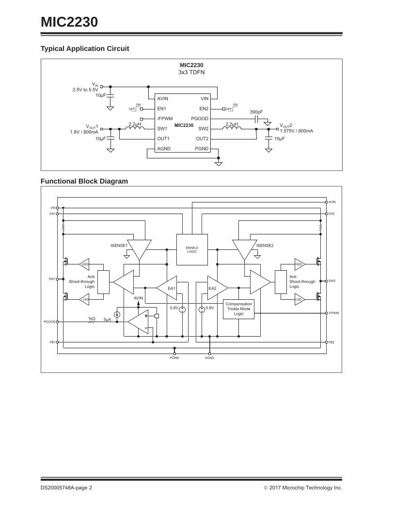
MIC22305.6 Efficiency ConsiderationsEfficiency is defined as the amount of useful outputpower, divided by the amount of power supplied.
EQUATION 5-2:
Maintaining high efficiency serves two purposes. Itreduces power dissipation in the power supply,reducing the need for heat sinks and thermal designconsiderations and it reduces consumption of currentfor battery powered applications. Reduced currentdraw from a battery increases the devices operatingtime and is critical in hand held devices.
There are two types of losses in switching converters:DC losses and switching losses. DC losses are simplythe power dissipation of I2R. Power is dissipated in thehigh-side switch during the on cycle. Power loss isequal to the high side MOSFET RDS(ON) multiplied bythe Switch Current2. During the off cycle, the low sideN-channel MOSFET conducts, also dissipating power.Device operating current also reduces efficiency. Theproduct of the quiescent (operating) current and thesupply voltage is another DC loss. The current requireddriving the gates on and off at a constant 2.5 MHzfrequency and the switching transitions make up theswitching losses.
FIGURE 5-1: MIC2230 Efficiency VOUT = 1.575.The figure above shows an efficiency curve. From noload to 100 mA, efficiency losses are dominated byquiescent current losses, gate drive and transitionlosses. By forcing the MIC2230 into Trickle Mode(/FPWM = High), the buck regulator significantlyreduces the required switching current by entering intoa PFM (Pulse Frequency Modulation) mode. Thissignificantly increases efficiency at low output currents.
Over 100 mA, efficiency loss is dominated by MOSFETRDS(ON) and inductor losses. Higher input supplyvoltages will increase the Gate-to-Source threshold onthe internal MOSFETs, reducing the internal RDS(ON).This improves efficiency by reducing DC losses in thedevice. All but the inductor losses are inherent to thedevice. In which case, inductor selection becomesincreasingly critical in efficiency calculations. As theinductors are reduced in size, the DC resistance (DCR)can become quite significant. The DCR losses can becalculated as shown in Equation 5-3.
EQUATION 5-3:
From that, the loss in efficiency due to inductorresistance can be calculated as shown in Equation 5-4.
EQUATION 5-4:
Efficiency loss due to DCR is minimal at light loads andgains significance as the load is increased. Inductorselection becomes a trade-off between efficiency andsize in this case.
5.7 Trickle Mode OperationTrickle Mode operation is achieved by clamping theminimum peak current to approximately 150 mA. Thisforces a PFM mode by comparing the output voltage tothe internal reference. If the feedback voltage is lessthan 0.8V, the MIC2230 turns on the high side until thepeak inductor current reaches approximately 150 mA.A separate comparator then monitors the outputvoltage. If the feedback voltage is greater than 0.8V,the high side switch is then used as a 10 μA currentsource, never turning off completely. This creates ahighly efficient light load mode by increasing the time ittakes for the output capacitor to discharge, delaying theamount of switching required and increasing light loadefficiency. While operating in this mode without anyload, the output voltage may rise over the nominaloperating voltage range. For applications that requiretight voltage tolerances, a minimum load of 150 μA isrecommended.
This load may either be used by the attached system,by lowering the feedback resistors or by adding anadditional load resistor in parallel with the outputcapacitor.
Efficiency_%V OUT IOUT
V IN I IN---------------------------------- 100=
L_Pd IOUT2 DCR=
Efficiency_Loss 1V OUT IOUT
V OUT IOUT L_Pd+------------------------------------------------------ – 100=

MIC2230
DS20005748A-page 16 2017 Microchip Technology Inc.
When the load current is greater than approximately100 mA, the MIC2230 automatically switches to PWMmode.
5.8 FPWM OperationIn forced PWM Mode (/FPWM = LOW) the MIC2230 isforced to provides constant switching at 2.5 MHz withsynchronous internal MOSFETs throughout the loadcurrent. In FPWM Mode, the output ripple can be aslow as 7 mV.

2017 Microchip Technology Inc. DS20005748A-page 17
MIC22306.0 MIC2230 EVALUATION BOARD SCHEMATIC
FIGURE 6-1: MIC2230 Adjustable Option (1.8V, 1.8V).
EN2
AVIN
FPWM
U1 MIC2230YML
FB2/Vo2
AGND
R3549k
L12.2μH
L22.2μH
R4442k
C410μF
SW2
EN1
VIN
PGOOD
FB1/Vo1
PGND
SW1
3
2
7
4
1
5
9
11
10
8
12
6
R1549k
R2442k
C522pF
J1+VIN 2.5V to 5.5V
J7EN2
J3VO21.8V
J2GND
C21μF
C110μF
C622pF
C710μF
C3390pF
J8EN1
J4PGOOD
J5VO11.8V
J6GND
TABLE 6-1: BILL OF MATERIALSItem Part Number Manufacturer Description Qty
C1 C1608X5R0J106K TDK 10 μF Ceramic Capacitor, 6.3V, X5R, Size 0603 1
C2 C1005X5R0J105K TDK 1 μF Ceramic Capacitor, 6.3V, X5R, Size 0402 1
C3 C0603Y391KXXA Vishay 390 pF Ceramic Capacitor, 25V, X7R, Size 0603 1
C4, C5 0603ZD106MAT AVX 10 μF Ceramic Capacitor, 6.3V, X5R, Size 0603 2
L1, L2
CDRH2D11/HPNP-2R2NC Sumida 2.2 μH, 1.1A ISAT., 120 mΩ,
(1.2 mm × 3.2 mm × 3.2 mm)
2LQH43CN2R2M03 Murata 2.2 μH, 900 mA ISAT., 110 mΩ, (2.6 mm × 3.2 mm × 4.5 mm)
EPL2014-222MLB Coilcraft 2.2 μH, 1.3A ISAT., 120 mΩ, (1.4 mm x 1.8 mm x 2.0 mm)
R2, R4 CRCW06034423FT1 Vishay 442 kΩ, 1%, Size 0603 2R1, R3 CRCW06035493FT1 Vishay 549 kΩ, 1%, Size 0603 2
U1 MIC2230-AAYML Microchip 2.5 MHz Dual Phase PWM Buck Regulator 1
L1, L2 CDRH2D11/HPNP-2R2NC Sumida 2.2 μH, 1.1A ISAT., 120 mΩ,
(1.2 mm × 3.2 mm × 3.2 mm) 2

MIC2230
DS20005748A-page 18 2017 Microchip Technology Inc.
7.0 PACKAGING INFORMATION
7.1 Package Marking Information
12-lead QFN* Example
AA22301246
XXXXXX
YWWY
Legend: XX...X Product code or customer-specific informationY Year code (last digit of calendar year)YY Year code (last 2 digits of calendar year)WW Week code (week of January 1 is week ‘01’)NNN Alphanumeric traceability code Pb-free JEDEC® designator for Matte Tin (Sn)* This package is Pb-free. The Pb-free JEDEC designator ( )
can be found on the outer packaging for this package.
●, ▲, ▼ Pin one index is identified by a dot, delta up, or delta down (trianglemark).
Note: In the event the full Microchip part number cannot be marked on one line, it willbe carried over to the next line, thus limiting the number of availablecharacters for customer-specific information. Package may or may not includethe corporate logo.
Underbar (_) and/or Overbar (‾) symbol may not be to scale.
3e
3e

2017 Microchip Technology Inc. DS20005748A-page 19
MIC2230
Note: For the most current package drawings, please see the Microchip Packaging Specification located at http://www.microchip.com/packaging.

MIC2230
DS20005748A-page 20 2017 Microchip Technology Inc.
Note: For the most current package drawings, please see the Microchip Packaging Specification located at http://www.microchip.com/packaging.

2017 Microchip Technology Inc. DS20005748A-page 21
MIC2230APPENDIX A: REVISION HISTORY
Revision A (April 2017)• Converted Micrel document MIC2230 to Micro-
chip data sheet template DS20005748A.• Minor grammatical text changes throughout.

MIC2230
DS20005748A-page 22 2017 Microchip Technology Inc.
NOTES:
2017 Microchip Technology Inc. DS20005748A-page 23
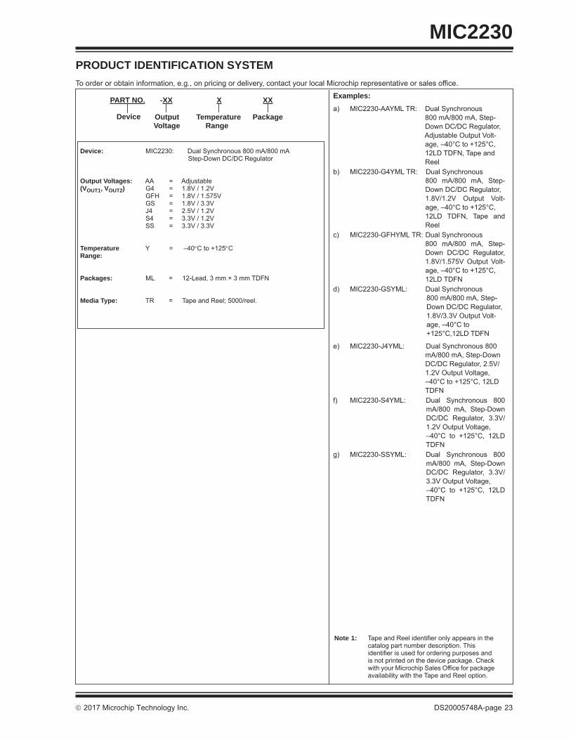
MIC2230PRODUCT IDENTIFICATION SYSTEMTo order or obtain information, e.g., on pricing or delivery, contact your local Microchip representative or sales office.
Examples:a) MIC2230-AAYML TR: Dual Synchronous
800 mA/800 mA, Step-Down DC/DC Regulator,Adjustable Output Volt-age, –40°C to +125°C,12LD TDFN, Tape and Reel
b) MIC2230-G4YML TR: Dual Synchronous 800 mA/800 mA, Step-Down DC/DC Regulator,1.8V/1.2V Output Volt-age, –40°C to +125°C,12LD TDFN, Tape andReel
c) MIC2230-GFHYML TR: Dual Synchronous 800 mA/800 mA, Step-Down DC/DC Regulator,1.8V/1.575V Output Volt-age, –40°C to +125°C,12LD TDFN
d) MIC2230-GSYML: Dual Synchronous 800 mA/800 mA, Step-Down DC/DC Regulator, 1.8V/3.3V Output Volt-age, –40°C to +125°C,12LD TDFN
e) MIC2230-J4YML: Dual Synchronous 800 mA/800 mA, Step-Down DC/DC Regulator, 2.5V/1.2V Output Voltage, –40°C to +125°C, 12LD TDFN
f) MIC2230-S4YML: Dual Synchronous 800mA/800 mA, Step-DownDC/DC Regulator, 3.3V/1.2V Output Voltage, –40°C to +125°C, 12LDTDFN
g) MIC2230-SSYML: Dual Synchronous 800mA/800 mA, Step-DownDC/DC Regulator, 3.3V/3.3V Output Voltage, –40°C to +125°C, 12LDTDFN
PART NO. X XX
PackageTemperatureRange
Device
Device: MIC2230: Dual Synchronous 800 mA/800 mAStep-Down DC/DC Regulator
Output Voltages:(VOUT1, VOUT2)
AA = AdjustableG4 = 1.8V / 1.2VGFH = 1.8V / 1.575VGS = 1.8V / 3.3VJ4 = 2.5V / 1.2VS4 = 3.3V / 1.2VSS = 3.3V / 3.3V
Temperature Range:
Y = –40C to +125C
Packages: ML = 12-Lead, 3 mm × 3 mm TDFN
Media Type: TR = Tape and Reel; 5000/reel.
Note 1: Tape and Reel identifier only appears in the catalog part number description. This identifier is used for ordering purposes and is not printed on the device package. Check with your Microchip Sales Office for package availability with the Tape and Reel option.
-XX
OutputVoltage

MIC2230
DS20005748A-page 24 2017 Microchip Technology Inc.
NOTES:

2017 Microchip Technology Inc. DS20005748A-page 25
Information contained in this publication regarding deviceapplications and the like is provided only for your convenienceand may be superseded by updates. It is your responsibility toensure that your application meets with your specifications.MICROCHIP MAKES NO REPRESENTATIONS ORWARRANTIES OF ANY KIND WHETHER EXPRESS ORIMPLIED, WRITTEN OR ORAL, STATUTORY OROTHERWISE, RELATED TO THE INFORMATION,INCLUDING BUT NOT LIMITED TO ITS CONDITION,QUALITY, PERFORMANCE, MERCHANTABILITY ORFITNESS FOR PURPOSE. Microchip disclaims all liabilityarising from this information and its use. Use of Microchipdevices in life support and/or safety applications is entirely atthe buyer’s risk, and the buyer agrees to defend, indemnify andhold harmless Microchip from any and all damages, claims,suits, or expenses resulting from such use. No licenses areconveyed, implicitly or otherwise, under any Microchipintellectual property rights unless otherwise stated.
Trademarks
The Microchip name and logo, the Microchip logo, AnyRate, dsPIC, FlashFlex, flexPWR, Heldo, JukeBlox, KeeLoq, KeeLoq logo, Kleer, LANCheck, LINK MD, MediaLB, MOST, MOST logo, MPLAB, OptoLyzer, PIC, PICSTART, PIC32 logo, RightTouch, SpyNIC, SST, SST Logo, SuperFlash and UNI/O are registered trademarks of Microchip Technology Incorporated in the U.S.A. and other countries.
ClockWorks, The Embedded Control Solutions Company, ETHERSYNCH, Hyper Speed Control, HyperLight Load, IntelliMOS, mTouch, Precision Edge, and QUIET-WIRE are registered trademarks of Microchip Technology Incorporated in the U.S.A.
Analog-for-the-Digital Age, Any Capacitor, AnyIn, AnyOut, BodyCom, chipKIT, chipKIT logo, CodeGuard, dsPICDEM, dsPICDEM.net, Dynamic Average Matching, DAM, ECAN, EtherGREEN, In-Circuit Serial Programming, ICSP, Inter-Chip Connectivity, JitterBlocker, KleerNet, KleerNet logo, MiWi, motorBench, MPASM, MPF, MPLAB Certified logo, MPLIB, MPLINK, MultiTRAK, NetDetach, Omniscient Code Generation, PICDEM, PICDEM.net, PICkit, PICtail, PureSilicon, RightTouch logo, REAL ICE, Ripple Blocker, Serial Quad I/O, SQI, SuperSwitcher, SuperSwitcher II, Total Endurance, TSHARC, USBCheck, VariSense, ViewSpan, WiperLock, Wireless DNA, and ZENA are trademarks of Microchip Technology Incorporated in the U.S.A. and other countries.
SQTP is a service mark of Microchip Technology Incorporated in the U.S.A.
Silicon Storage Technology is a registered trademark of Microchip Technology Inc. in other countries.
GestIC is a registered trademarks of Microchip Technology Germany II GmbH & Co. KG, a subsidiary of Microchip Technology Inc., in other countries.
All other trademarks mentioned herein are property of their respective companies.
© 2017, Microchip Technology Incorporated, Printed in the U.S.A., All Rights Reserved.
ISBN: 978-1-5224-1653-1
Note the following details of the code protection feature on Microchip devices:• Microchip products meet the specification contained in their particular Microchip Data Sheet.
• Microchip believes that its family of products is one of the most secure families of its kind on the market today, when used in the intended manner and under normal conditions.
• There are dishonest and possibly illegal methods used to breach the code protection feature. All of these methods, to our knowledge, require using the Microchip products in a manner outside the operating specifications contained in Microchip’s Data Sheets. Most likely, the person doing so is engaged in theft of intellectual property.
• Microchip is willing to work with the customer who is concerned about the integrity of their code.
• Neither Microchip nor any other semiconductor manufacturer can guarantee the security of their code. Code protection does not mean that we are guaranteeing the product as “unbreakable.”
Code protection is constantly evolving. We at Microchip are committed to continuously improving the code protection features of ourproducts. Attempts to break Microchip’s code protection feature may be a violation of the Digital Millennium Copyright Act. If such actsallow unauthorized access to your software or other copyrighted work, you may have a right to sue for relief under that Act.
Microchip received ISO/TS-16949:2009 certification for its worldwide headquarters, design and wafer fabrication facilities in Chandler and Tempe, Arizona; Gresham, Oregon and design centers in California and India. The Company’s quality system processes and procedures are for its PIC® MCUs and dsPIC® DSCs, KEELOQ® code hopping devices, Serial EEPROMs, microperipherals, nonvolatile memory and analog products. In addition, Microchip’s quality system for the design and manufacture of development systems is ISO 9001:2000 certified.

DS20005748A-page 26 2017 Microchip Technology Inc.
AMERICASCorporate Office2355 West Chandler Blvd.Chandler, AZ 85224-6199Tel: 480-792-7200 Fax: 480-792-7277Technical Support: http://www.microchip.com/supportWeb Address: www.microchip.comAtlantaDuluth, GA Tel: 678-957-9614 Fax: 678-957-1455Austin, TXTel: 512-257-3370 BostonWestborough, MA Tel: 774-760-0087 Fax: 774-760-0088ChicagoItasca, IL Tel: 630-285-0071 Fax: 630-285-0075DallasAddison, TX Tel: 972-818-7423 Fax: 972-818-2924DetroitNovi, MI Tel: 248-848-4000Houston, TX Tel: 281-894-5983IndianapolisNoblesville, IN Tel: 317-773-8323Fax: 317-773-5453Tel: 317-536-2380Los AngelesMission Viejo, CA Tel: 949-462-9523Fax: 949-462-9608Tel: 951-273-7800 Raleigh, NC Tel: 919-844-7510New York, NY Tel: 631-435-6000San Jose, CA Tel: 408-735-9110Tel: 408-436-4270Canada - TorontoTel: 905-695-1980 Fax: 905-695-2078
ASIA/PACIFICAsia Pacific OfficeSuites 3707-14, 37th FloorTower 6, The GatewayHarbour City, KowloonHong KongTel: 852-2943-5100Fax: 852-2401-3431Australia - SydneyTel: 61-2-9868-6733Fax: 61-2-9868-6755China - BeijingTel: 86-10-8569-7000 Fax: 86-10-8528-2104China - ChengduTel: 86-28-8665-5511Fax: 86-28-8665-7889China - ChongqingTel: 86-23-8980-9588Fax: 86-23-8980-9500China - DongguanTel: 86-769-8702-9880 China - GuangzhouTel: 86-20-8755-8029 China - HangzhouTel: 86-571-8792-8115 Fax: 86-571-8792-8116China - Hong Kong SARTel: 852-2943-5100 Fax: 852-2401-3431China - NanjingTel: 86-25-8473-2460Fax: 86-25-8473-2470China - QingdaoTel: 86-532-8502-7355Fax: 86-532-8502-7205China - ShanghaiTel: 86-21-3326-8000 Fax: 86-21-3326-8021China - ShenyangTel: 86-24-2334-2829Fax: 86-24-2334-2393China - ShenzhenTel: 86-755-8864-2200 Fax: 86-755-8203-1760China - WuhanTel: 86-27-5980-5300Fax: 86-27-5980-5118China - XianTel: 86-29-8833-7252Fax: 86-29-8833-7256
ASIA/PACIFICChina - XiamenTel: 86-592-2388138 Fax: 86-592-2388130China - ZhuhaiTel: 86-756-3210040 Fax: 86-756-3210049India - BangaloreTel: 91-80-3090-4444 Fax: 91-80-3090-4123India - New DelhiTel: 91-11-4160-8631Fax: 91-11-4160-8632India - PuneTel: 91-20-3019-1500Japan - OsakaTel: 81-6-6152-7160 Fax: 81-6-6152-9310Japan - TokyoTel: 81-3-6880- 3770 Fax: 81-3-6880-3771Korea - DaeguTel: 82-53-744-4301Fax: 82-53-744-4302Korea - SeoulTel: 82-2-554-7200Fax: 82-2-558-5932 or 82-2-558-5934Malaysia - Kuala LumpurTel: 60-3-6201-9857Fax: 60-3-6201-9859Malaysia - PenangTel: 60-4-227-8870Fax: 60-4-227-4068Philippines - ManilaTel: 63-2-634-9065Fax: 63-2-634-9069SingaporeTel: 65-6334-8870Fax: 65-6334-8850Taiwan - Hsin ChuTel: 886-3-5778-366Fax: 886-3-5770-955Taiwan - KaohsiungTel: 886-7-213-7830Taiwan - TaipeiTel: 886-2-2508-8600 Fax: 886-2-2508-0102Thailand - BangkokTel: 66-2-694-1351Fax: 66-2-694-1350
EUROPEAustria - WelsTel: 43-7242-2244-39Fax: 43-7242-2244-393Denmark - CopenhagenTel: 45-4450-2828 Fax: 45-4485-2829Finland - EspooTel: 358-9-4520-820France - ParisTel: 33-1-69-53-63-20 Fax: 33-1-69-30-90-79France - Saint CloudTel: 33-1-30-60-70-00 Germany - GarchingTel: 49-8931-9700Germany - HaanTel: 49-2129-3766400Germany - HeilbronnTel: 49-7131-67-3636Germany - KarlsruheTel: 49-721-625370Germany - MunichTel: 49-89-627-144-0 Fax: 49-89-627-144-44Germany - RosenheimTel: 49-8031-354-560Israel - Ra’anana Tel: 972-9-744-7705Italy - Milan Tel: 39-0331-742611 Fax: 39-0331-466781Italy - PadovaTel: 39-049-7625286 Netherlands - DrunenTel: 31-416-690399 Fax: 31-416-690340Norway - TrondheimTel: 47-7289-7561Poland - WarsawTel: 48-22-3325737 Romania - BucharestTel: 40-21-407-87-50Spain - MadridTel: 34-91-708-08-90Fax: 34-91-708-08-91Sweden - GothenbergTel: 46-31-704-60-40Sweden - StockholmTel: 46-8-5090-4654UK - WokinghamTel: 44-118-921-5800Fax: 44-118-921-5820
Worldwide Sales and Service
11/07/16
Recommended