1662 IEEE TRANSACTIONS ON INDUSTRY APPLICATIONS, VOL. 48, NO. 5, SEPTEMBER/OCTOBER 2012
Simple Transfer Technology for Fabricationof TFT Backplane for Flexible Displays
Toshihiro Yamamoto, Tatsuya Takei, Yoshiki Nakajima, Yoshihide Fujisaki, Tadahiro Furukawa,Masayuki Hosoi, Akihiro Kinoshita, and Hideo Fujikake, Member, IEEE
Abstract—A new simple transfer technology for the realizationof flexible thin-film transistors (TFTs) on a plastic substrate hasbeen developed. The basic principle of the proposed method isthat, after all the fabrication processes for the TFT array on atemporary adhesive layer coated on a glass substrate have beencompleted, the TFT is then transferred onto a plastic film. A 5.8-in-diagonal wide-quarter quarter video graphics array (QVGA) or-ganic TFT array and a 5-in-diagonal QVGA oxide TFT array werefabricated on the temporary adhesive layer. We confirmed that thedegree of substrate deformation for the proposed technology wasless than that for the conventional direct formation method. Wealso transferred both TFT arrays to plastic films and confirmedthat no significant degradation in the electrical characteristics ofthe TFTs has occurred as a result of the transfer process. It isconsidered that this will be a key technology for the fabricationof large flexible displays with TFT backplanes.
Index Terms—Deformation rate, flexible display, low-temperature fabrication, manufacturing processes, organiclight-emitting diodes (OLEDs), organic thin-film transistor (TFT),oxide TFT, plastic film, transfer method.
I. INTRODUCTION
THIN and lightweight flexible displays are expected to behighly suitable for the mobile equipment of advanced
digital broadcasting services because of their high portability.Much research is currently being directed toward the develop-ment of flexible displays, which are more useful for mobileequipment than rigid glass-based displays [1]–[5]. We havebeen developing thin-film transistor (TFT)-driven organic light-emitting diode (OLED) displays on plastic films and have re-cently fabricated a 5-in-diagonal flexible quarter video graphicsarray (QVGA) OLED display [6]. However, the realization oflarger flexible displays is desirable.
Manuscript received June 30, 2011; revised January 23, 2012; acceptedFebruary 29, 2012. Date of publication July 17, 2012; date of current versionSeptember 14, 2012. Paper 20111-ILDC-330.R1, presented at the 2011 IEEEIndustry Applications Society Annual Meeting, Orlando, FL, October 9–13,and approved for publication in the IEEE TRANSACTIONS ON INDUSTRY
APPLICATIONS by the Industrial Lighting and Display Committee of the IEEEIndustry Applications Society.
T. Yamamoto, T. Takei, Y. Nakajima, Y. Fujisaki, and H. Fujikake are withJapan Broadcasting Corporation (NHK), Tokyo 157-8510, Japan (e-mail:[email protected]; [email protected]; [email protected];[email protected]; [email protected]).
T. Furukawa is with Yamagata University, Yamagata 990-8560, Japan (email:[email protected]).
M. Hosoi and A. Kinoshita are with Kyodo Printing Company, Ltd., Tokyo112-8501, Japan (e-mail: [email protected]; [email protected]).
Color versions of one or more of the figures in this paper are available onlineat http://ieeexplore.ieee.org.
Digital Object Identifier 10.1109/TIA.2012.2209170
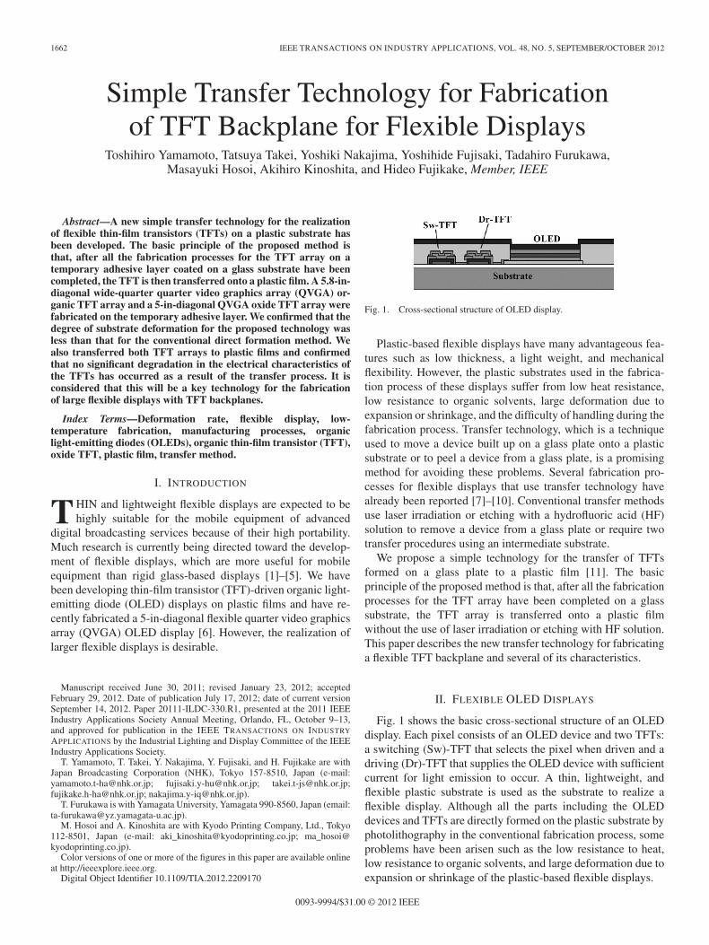
Fig. 1. Cross-sectional structure of OLED display.
Plastic-based flexible displays have many advantageous fea-tures such as low thickness, a light weight, and mechanicalflexibility. However, the plastic substrates used in the fabrica-tion process of these displays suffer from low heat resistance,low resistance to organic solvents, large deformation due toexpansion or shrinkage, and the difficulty of handling during thefabrication process. Transfer technology, which is a techniqueused to move a device built up on a glass plate onto a plasticsubstrate or to peel a device from a glass plate, is a promisingmethod for avoiding these problems. Several fabrication pro-cesses for flexible displays that use transfer technology havealready been reported [7]–[10]. Conventional transfer methodsuse laser irradiation or etching with a hydrofluoric acid (HF)solution to remove a device from a glass plate or require twotransfer procedures using an intermediate substrate.
We propose a simple technology for the transfer of TFTsformed on a glass plate to a plastic film [11]. The basicprinciple of the proposed method is that, after all the fabricationprocesses for the TFT array have been completed on a glasssubstrate, the TFT array is transferred onto a plastic filmwithout the use of laser irradiation or etching with HF solution.This paper describes the new transfer technology for fabricatinga flexible TFT backplane and several of its characteristics.
II. FLEXIBLE OLED DISPLAYS
Fig. 1 shows the basic cross-sectional structure of an OLEDdisplay. Each pixel consists of an OLED device and two TFTs:a switching (Sw)-TFT that selects the pixel when driven and adriving (Dr)-TFT that supplies the OLED device with sufficientcurrent for light emission to occur. A thin, lightweight, andflexible plastic substrate is used as the substrate to realize aflexible display. Although all the parts including the OLEDdevices and TFTs are directly formed on the plastic substrate byphotolithography in the conventional fabrication process, someproblems have been arisen such as the low resistance to heat,low resistance to organic solvents, and large deformation due toexpansion or shrinkage of the plastic-based flexible displays.
0093-9994/$31.00 © 2012 IEEE
YAMAMOTO et al.: SIMPLE TRANSFER TECHNOLOGY FOR FABRICATION OF TFT BACKPLANE FOR FLEXIBLE DISPLAYS 1663
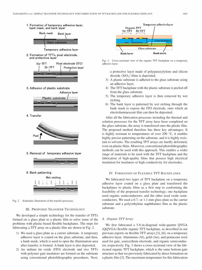
Fig. 2. Schematic illustration of the transfer processes.
III. PROPOSED TRANSFER TECHNOLOGY
We developed a simple technology for the transfer of TFTsformed on a glass plate to a plastic film to solve some of theproblems with plastic-based flexible backplanes. The steps forfabricating a TFT array on a plastic film are shown in Fig. 2.
1) We used a glass plate as a carrier substrate. A temporaryadhesive layer is coated on the glass substrate, and then,a bank mask, which is used to open the illumination areaafter transfer, is formed. A bank layer is also deposited.
2) An indium tin oxide (ITO) electrode and two TFTswith polymer gate insulators are formed on the substrateusing conventional photolithographic procedures. Next,
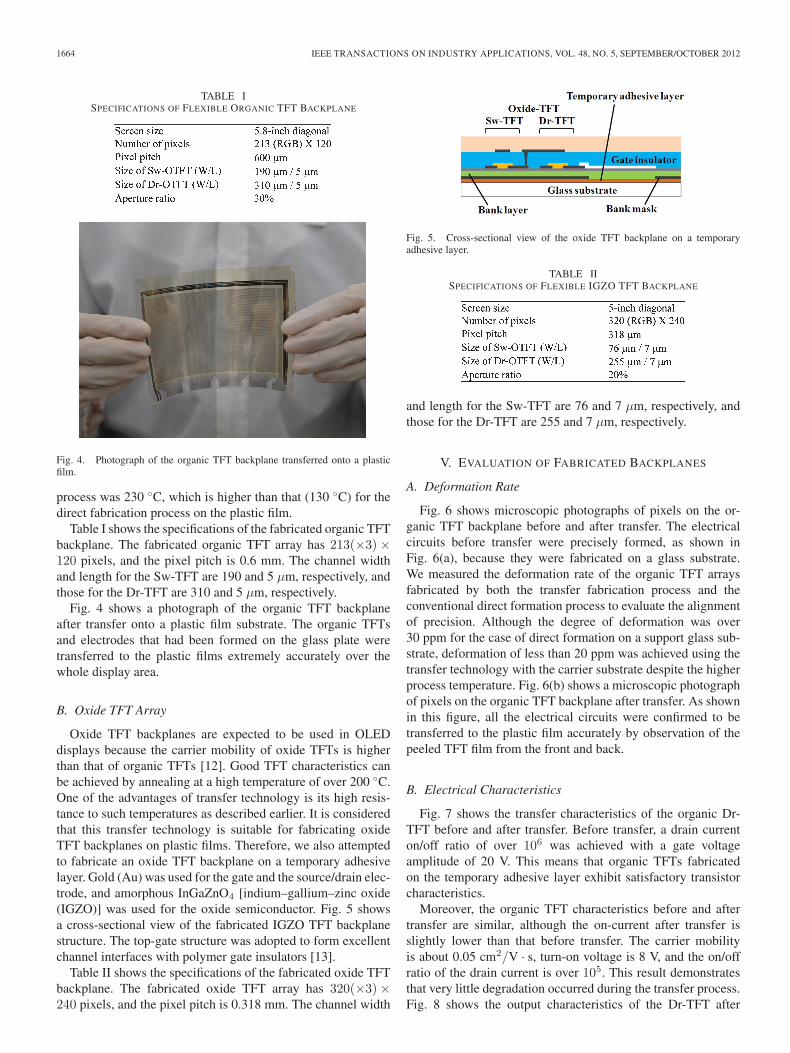
Fig. 3. Cross-sectional view of the organic TFT backplane on a temporaryadhesive layer.
a protective layer made of polyparaxylylene and silicondioxide (SiO2) films is deposited.
3) A plastic substrate is adhered to the glass substrate usingan adhesive layer.
4) The TFT backplane with the plastic substrate is peeled offfrom the glass substrate.
5) The temporary adhesive layer is then removed by wetetching.
6) The bank layer is patterned by wet etching through thebank mask to expose the ITO electrode, onto which anelectroluminescent film can then be deposited.
After all the fabrication processes including the thermal andsolution processes for the TFT array have been completed onthe glass substrate, the array is transferred onto the plastic film.The proposed method therefore has three key advantages: Itis highly resistant to temperatures of over 200 ◦C, it enableshighly precise patterning on the substrate, and it is highly resis-tant to solvents. The resulting TFT arrays are hardly deformed,even on plastic films. Moreover, conventional photolithographicmethods can be used with this approach. This enables a widerrange of materials to be used with the TFT backplane and thefabrication of high-quality films that possess high electricalinsulation for insulators or high conductivity for electrodes.
IV. FORMATION OF FLEXIBLE TFT BACKPLANES
We fabricated two types of TFT backplane on a temporaryadhesive layer coated on a glass plate and transferred thebackplanes to plastic films as a first step to conforming thefeasibility of the proposed transfer technology; one backplaneused organic semiconductors, and the other used oxide semi-conductors. We used a 0.7- or 1.1-mm glass plate as the carriersubstrate and a poly(ethylene naphthalate) film as the plasticsubstrate.
A. Organic TFT Array
We first fabricated a 5.8-in-diagonal wide-quarter QVGA(QQVGA) flexible organic TFT backplane, as described in ourprevious reports on flexible TFT arrays [3], [6], on a temporaryadhesive layer. Aluminum (Al), gold (Au), and pentacene wereused for gate, source/drain electrode, and organic semiconduc-tor, respectively. Fig. 3 shows a cross-sectional view of the fab-ricated organic TFT backplane, which is the same bottom-gatestructure as that we previously fabricated by direct formation ona plastic film [3]. The maximum temperature for this fabrication
1664 IEEE TRANSACTIONS ON INDUSTRY APPLICATIONS, VOL. 48, NO. 5, SEPTEMBER/OCTOBER 2012
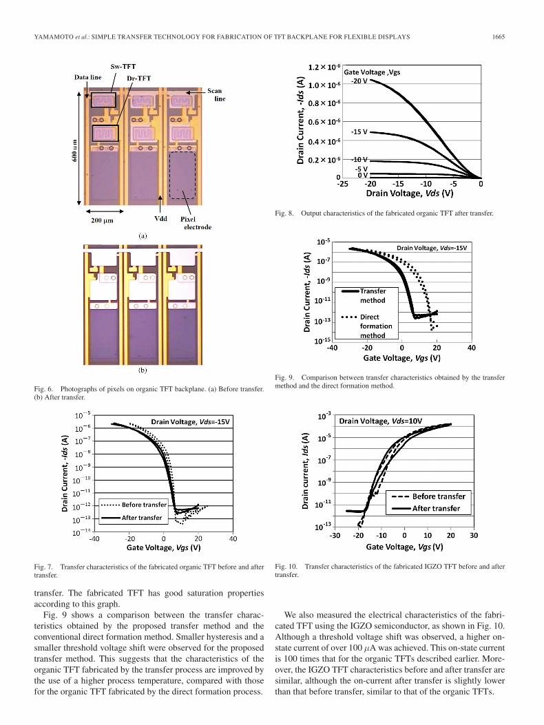
TABLE ISPECIFICATIONS OF FLEXIBLE ORGANIC TFT BACKPLANE
Fig. 4. Photograph of the organic TFT backplane transferred onto a plasticfilm.
process was 230 ◦C, which is higher than that (130 ◦C) for thedirect fabrication process on the plastic film.
Table I shows the specifications of the fabricated organic TFTbackplane. The fabricated organic TFT array has 213(×3)×120 pixels, and the pixel pitch is 0.6 mm. The channel widthand length for the Sw-TFT are 190 and 5 µm, respectively, andthose for the Dr-TFT are 310 and 5 µm, respectively.
Fig. 4 shows a photograph of the organic TFT backplaneafter transfer onto a plastic film substrate. The organic TFTsand electrodes that had been formed on the glass plate weretransferred to the plastic films extremely accurately over thewhole display area.
B. Oxide TFT Array
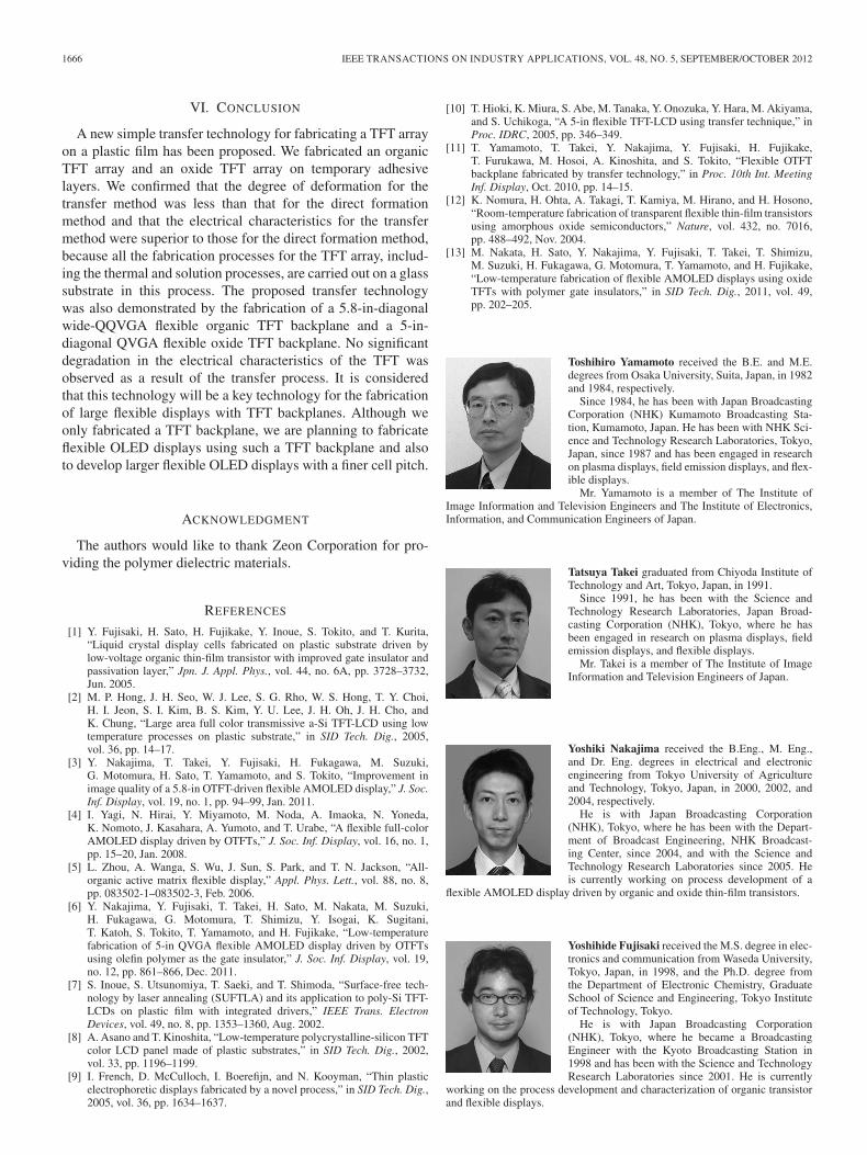
Oxide TFT backplanes are expected to be used in OLEDdisplays because the carrier mobility of oxide TFTs is higherthan that of organic TFTs [12]. Good TFT characteristics canbe achieved by annealing at a high temperature of over 200 ◦C.One of the advantages of transfer technology is its high resis-tance to such temperatures as described earlier. It is consideredthat this transfer technology is suitable for fabricating oxideTFT backplanes on plastic films. Therefore, we also attemptedto fabricate an oxide TFT backplane on a temporary adhesivelayer. Gold (Au) was used for the gate and the source/drain elec-trode, and amorphous InGaZnO4 [indium–gallium–zinc oxide(IGZO)] was used for the oxide semiconductor. Fig. 5 showsa cross-sectional view of the fabricated IGZO TFT backplanestructure. The top-gate structure was adopted to form excellentchannel interfaces with polymer gate insulators [13].
Table II shows the specifications of the fabricated oxide TFTbackplane. The fabricated oxide TFT array has 320(×3)×240 pixels, and the pixel pitch is 0.318 mm. The channel width
Fig. 5. Cross-sectional view of the oxide TFT backplane on a temporaryadhesive layer.
TABLE IISPECIFICATIONS OF FLEXIBLE IGZO TFT BACKPLANE
and length for the Sw-TFT are 76 and 7 µm, respectively, andthose for the Dr-TFT are 255 and 7 µm, respectively.
V. EVALUATION OF FABRICATED BACKPLANES
A. Deformation Rate
Fig. 6 shows microscopic photographs of pixels on the or-ganic TFT backplane before and after transfer. The electricalcircuits before transfer were precisely formed, as shown inFig. 6(a), because they were fabricated on a glass substrate.We measured the deformation rate of the organic TFT arraysfabricated by both the transfer fabrication process and theconventional direct formation process to evaluate the alignmentof precision. Although the degree of deformation was over30 ppm for the case of direct formation on a support glass sub-strate, deformation of less than 20 ppm was achieved using thetransfer technology with the carrier substrate despite the higherprocess temperature. Fig. 6(b) shows a microscopic photographof pixels on the organic TFT backplane after transfer. As shownin this figure, all the electrical circuits were confirmed to betransferred to the plastic film accurately by observation of thepeeled TFT film from the front and back.
B. Electrical Characteristics
Fig. 7 shows the transfer characteristics of the organic Dr-TFT before and after transfer. Before transfer, a drain currenton/off ratio of over 106 was achieved with a gate voltageamplitude of 20 V. This means that organic TFTs fabricatedon the temporary adhesive layer exhibit satisfactory transistorcharacteristics.
Moreover, the organic TFT characteristics before and aftertransfer are similar, although the on-current after transfer isslightly lower than that before transfer. The carrier mobilityis about 0.05 cm2/V · s, turn-on voltage is 8 V, and the on/offratio of the drain current is over 105. This result demonstratesthat very little degradation occurred during the transfer process.Fig. 8 shows the output characteristics of the Dr-TFT after
YAMAMOTO et al.: SIMPLE TRANSFER TECHNOLOGY FOR FABRICATION OF TFT BACKPLANE FOR FLEXIBLE DISPLAYS 1665
Fig. 6. Photographs of pixels on organic TFT backplane. (a) Before transfer.(b) After transfer.
Fig. 7. Transfer characteristics of the fabricated organic TFT before and aftertransfer.
transfer. The fabricated TFT has good saturation propertiesaccording to this graph.
Fig. 9 shows a comparison between the transfer charac-teristics obtained by the proposed transfer method and theconventional direct formation method. Smaller hysteresis and asmaller threshold voltage shift were observed for the proposedtransfer method. This suggests that the characteristics of theorganic TFT fabricated by the transfer process are improved bythe use of a higher process temperature, compared with thosefor the organic TFT fabricated by the direct formation process.
Fig. 8. Output characteristics of the fabricated organic TFT after transfer.
Fig. 9. Comparison between transfer characteristics obtained by the transfermethod and the direct formation method.
Fig. 10. Transfer characteristics of the fabricated IGZO TFT before and aftertransfer.
We also measured the electrical characteristics of the fabri-cated TFT using the IGZO semiconductor, as shown in Fig. 10.Although a threshold voltage shift was observed, a higher on-state current of over 100 µA was achieved. This on-state currentis 100 times that for the organic TFTs described earlier. More-over, the IGZO TFT characteristics before and after transfer aresimilar, although the on-current after transfer is slightly lowerthan that before transfer, similar to that of the organic TFTs.
1666 IEEE TRANSACTIONS ON INDUSTRY APPLICATIONS, VOL. 48, NO. 5, SEPTEMBER/OCTOBER 2012
VI. CONCLUSION
A new simple transfer technology for fabricating a TFT arrayon a plastic film has been proposed. We fabricated an organicTFT array and an oxide TFT array on temporary adhesivelayers. We confirmed that the degree of deformation for thetransfer method was less than that for the direct formationmethod and that the electrical characteristics for the transfermethod were superior to those for the direct formation method,because all the fabrication processes for the TFT array, includ-ing the thermal and solution processes, are carried out on a glasssubstrate in this process. The proposed transfer technologywas also demonstrated by the fabrication of a 5.8-in-diagonalwide-QQVGA flexible organic TFT backplane and a 5-in-diagonal QVGA flexible oxide TFT backplane. No significantdegradation in the electrical characteristics of the TFT wasobserved as a result of the transfer process. It is consideredthat this technology will be a key technology for the fabricationof large flexible displays with TFT backplanes. Although weonly fabricated a TFT backplane, we are planning to fabricateflexible OLED displays using such a TFT backplane and alsoto develop larger flexible OLED displays with a finer cell pitch.
ACKNOWLEDGMENT
The authors would like to thank Zeon Corporation for pro-viding the polymer dielectric materials.
REFERENCES
[1] Y. Fujisaki, H. Sato, H. Fujikake, Y. Inoue, S. Tokito, and T. Kurita,“Liquid crystal display cells fabricated on plastic substrate driven bylow-voltage organic thin-film transistor with improved gate insulator andpassivation layer,” Jpn. J. Appl. Phys., vol. 44, no. 6A, pp. 3728–3732,Jun. 2005.
[2] M. P. Hong, J. H. Seo, W. J. Lee, S. G. Rho, W. S. Hong, T. Y. Choi,H. I. Jeon, S. I. Kim, B. S. Kim, Y. U. Lee, J. H. Oh, J. H. Cho, andK. Chung, “Large area full color transmissive a-Si TFT-LCD using lowtemperature processes on plastic substrate,” in SID Tech. Dig., 2005,vol. 36, pp. 14–17.
[3] Y. Nakajima, T. Takei, Y. Fujisaki, H. Fukagawa, M. Suzuki,G. Motomura, H. Sato, T. Yamamoto, and S. Tokito, “Improvement inimage quality of a 5.8-in OTFT-driven flexible AMOLED display,” J. Soc.Inf. Display, vol. 19, no. 1, pp. 94–99, Jan. 2011.
[4] I. Yagi, N. Hirai, Y. Miyamoto, M. Noda, A. Imaoka, N. Yoneda,K. Nomoto, J. Kasahara, A. Yumoto, and T. Urabe, “A flexible full-colorAMOLED display driven by OTFTs,” J. Soc. Inf. Display, vol. 16, no. 1,pp. 15–20, Jan. 2008.
[5] L. Zhou, A. Wanga, S. Wu, J. Sun, S. Park, and T. N. Jackson, “All-organic active matrix flexible display,” Appl. Phys. Lett., vol. 88, no. 8,pp. 083502-1–083502-3, Feb. 2006.
[6] Y. Nakajima, Y. Fujisaki, T. Takei, H. Sato, M. Nakata, M. Suzuki,H. Fukagawa, G. Motomura, T. Shimizu, Y. Isogai, K. Sugitani,T. Katoh, S. Tokito, T. Yamamoto, and H. Fujikake, “Low-temperaturefabrication of 5-in QVGA flexible AMOLED display driven by OTFTsusing olefin polymer as the gate insulator,” J. Soc. Inf. Display, vol. 19,no. 12, pp. 861–866, Dec. 2011.
[7] S. Inoue, S. Utsunomiya, T. Saeki, and T. Shimoda, “Surface-free tech-nology by laser annealing (SUFTLA) and its application to poly-Si TFT-LCDs on plastic film with integrated drivers,” IEEE Trans. ElectronDevices, vol. 49, no. 8, pp. 1353–1360, Aug. 2002.
[8] A. Asano and T. Kinoshita, “Low-temperature polycrystalline-silicon TFTcolor LCD panel made of plastic substrates,” in SID Tech. Dig., 2002,vol. 33, pp. 1196–1199.
[9] I. French, D. McCulloch, I. Boerefijn, and N. Kooyman, “Thin plasticelectrophoretic displays fabricated by a novel process,” in SID Tech. Dig.,2005, vol. 36, pp. 1634–1637.
[10] T. Hioki, K. Miura, S. Abe, M. Tanaka, Y. Onozuka, Y. Hara, M. Akiyama,and S. Uchikoga, “A 5-in flexible TFT-LCD using transfer technique,” inProc. IDRC, 2005, pp. 346–349.
[11] T. Yamamoto, T. Takei, Y. Nakajima, Y. Fujisaki, H. Fujikake,T. Furukawa, M. Hosoi, A. Kinoshita, and S. Tokito, “Flexible OTFTbackplane fabricated by transfer technology,” in Proc. 10th Int. MeetingInf. Display, Oct. 2010, pp. 14–15.
[12] K. Nomura, H. Ohta, A. Takagi, T. Kamiya, M. Hirano, and H. Hosono,“Room-temperature fabrication of transparent flexible thin-film transistorsusing amorphous oxide semiconductors,” Nature, vol. 432, no. 7016,pp. 488–492, Nov. 2004.
[13] M. Nakata, H. Sato, Y. Nakajima, Y. Fujisaki, T. Takei, T. Shimizu,M. Suzuki, H. Fukagawa, G. Motomura, T. Yamamoto, and H. Fujikake,“Low-temperature fabrication of flexible AMOLED displays using oxideTFTs with polymer gate insulators,” in SID Tech. Dig., 2011, vol. 49,pp. 202–205.
Toshihiro Yamamoto received the B.E. and M.E.degrees from Osaka University, Suita, Japan, in 1982and 1984, respectively.
Since 1984, he has been with Japan BroadcastingCorporation (NHK) Kumamoto Broadcasting Sta-tion, Kumamoto, Japan. He has been with NHK Sci-ence and Technology Research Laboratories, Tokyo,Japan, since 1987 and has been engaged in researchon plasma displays, field emission displays, and flex-ible displays.
Mr. Yamamoto is a member of The Institute ofImage Information and Television Engineers and The Institute of Electronics,Information, and Communication Engineers of Japan.
Tatsuya Takei graduated from Chiyoda Institute ofTechnology and Art, Tokyo, Japan, in 1991.
Since 1991, he has been with the Science andTechnology Research Laboratories, Japan Broad-casting Corporation (NHK), Tokyo, where he hasbeen engaged in research on plasma displays, fieldemission displays, and flexible displays.
Mr. Takei is a member of The Institute of ImageInformation and Television Engineers of Japan.
Yoshiki Nakajima received the B.Eng., M. Eng.,and Dr. Eng. degrees in electrical and electronicengineering from Tokyo University of Agricultureand Technology, Tokyo, Japan, in 2000, 2002, and2004, respectively.
He is with Japan Broadcasting Corporation(NHK), Tokyo, where he has been with the Depart-ment of Broadcast Engineering, NHK Broadcast-ing Center, since 2004, and with the Science andTechnology Research Laboratories since 2005. Heis currently working on process development of a
flexible AMOLED display driven by organic and oxide thin-film transistors.
Yoshihide Fujisaki received the M.S. degree in elec-tronics and communication from Waseda University,Tokyo, Japan, in 1998, and the Ph.D. degree fromthe Department of Electronic Chemistry, GraduateSchool of Science and Engineering, Tokyo Instituteof Technology, Tokyo.
He is with Japan Broadcasting Corporation(NHK), Tokyo, where he became a BroadcastingEngineer with the Kyoto Broadcasting Station in1998 and has been with the Science and TechnologyResearch Laboratories since 2001. He is currently
working on the process development and characterization of organic transistorand flexible displays.
YAMAMOTO et al.: SIMPLE TRANSFER TECHNOLOGY FOR FABRICATION OF TFT BACKPLANE FOR FLEXIBLE DISPLAYS 1667
Tadahiro Furukawa received B.E. and M.E. de-grees from Saitama University, Saitama, Japan, in1982 and 1984, respectively.
Since 1984, he has been with Kyodo PrintingCompany, Ltd., Tokyo, Japan. He is concerned withdevelopment and production engineering of colorfilters for LCDs for the long term, and he has devel-oped the color filter and the backplane on the plasticsubstrate by the transfer method. Since 2011, hehas also been with Yamagata University, Yamagata,Japan.
Mr. Furukawa is a member of The Institute of Image Information andTelevision Engineers of Japan.
Masayuki Hosoi has been with Kyodo PrintingCompany, Ltd., Tokyo, Japan, since 1990, where hehad been engaged in manufacturing display compo-nents until 1999 and, since then, has been with theTechnical Supervisory Division.
Akihiro Kinoshita received the B.E. and M.E. de-grees from Nihon University, Tokyo, Japan, in 2006and 2008, respectively.
Since 2008, he has been with the Technical Su-pervisory Division, Kyodo Printing Company, Ltd.,Tokyo.
Hideo Fujikake (M’09) received the B.E., M.E.,and Dr.Eng. degrees in electronic engineering fromTohoku University, Sendai, Japan, in 1983, 1985, and2003, respectively.
He is with Japan Broadcasting Corporation(NHK), Tokyo, Japan, where he joined the Naganostation in 1985 as a Video Engineer and has beenwith the Science and Technology Research Labo-ratories since 1988, where he is currently a SeniorResearch Engineer, has been involved in research onflexible display technology, and has been engaged in
research and development of liquid crystal materials/devices and organic elec-tronic devices for displays and optical devices, including projection displays,flexible displays, optical filters, optical information processing, and broadcastprogram production applications. In 2006–2012, he was a Visiting Professor atTokyo University of Science, Tokyo.
Dr. Fujikake is a member of the Japanese Liquid Crystal Society; The JapanSociety of Applied Physics; The Institute of Electronics, Information, andCommunication Engineers of Japan; The Institute of Image Information andTelevision Engineers; The Illuminating Engineering Institute of Japan; and TheSociety for Information Display.
Recommended