Structural, Compositional and Optical Propertiesof Self-Organised Ge Quantum Dots
A. Dunbar1) (a), U. Bangert (a), P. Dawson (a), M. Halsall (a), Y. Shiraki (b),
M. Miura (b), I. Berbezier (c), B.A. Joyce (d), and J. Zhang (d)
(a) Department of Physics, UMIST, Manchester, M60 1QD, UK
(b) RCAST, The University of Tokyo, 4-6-1 Komaba, Meguro-ku, Tokyo 153, Japan
(c) CRMC2, Campus de Luminy, case 913, F-13288, Marseille, Cedex 9, France
(d) Physics Department, Imperial College London, Prince Consort Road, London, UK
(Received July 31, 2000; accepted October 2, 2000)
Subject classification: 68.37.Lp; 68.37.Ps; 68.65.Hb; 78.47.+p; 78.55.Ap; 78.67.Hc; S5.12
In this paper we present a study of the structure, composition and optical properties of SiGe quan-tum dots, grown by gas-source molecular beam epitaxy on Si (001). Atomic force microscopy(AFM), transmission electron microscopy (TEM), scanning transmission electron microscopy(STEM), energy dispersive X-ray analysis (EDX), photoluminescence (PL) spectroscopy and de-cay time measurements of the quantum dots suggest that there are two distinct sizes of quantumdot, contributing two distinct emission bands in the PL spectra.
1. Introduction The growth of self-organised Ge quantum dots on Si has attracted agreat deal of attention because of their potential application in Si based opto-electronicdevices. Confinement of carriers in the quantum dots is expected to increase the lumi-nescence efficiency [1, 2], due to the discrete nature of the confined states. Develop-ment of an efficient Si based light emitting material would make it possible to combineboth optical and electronic components on the same Si substrate. Various methods offabricating Ge quantum dots on Si substrates have been studied [3] but here we areconcerned only with self organised quantum dots grown by molecular beam epitaxy(MBE). Two types of quantum dots have been commonly reported [4]: small pyramidaldots and larger domes. A broad photoluminescence (PL) band centred at �0.8 eV,from Ge quantum dots has been reported [1, 5], but the nature of the recombinationprocesses occurring therein is not completely understood. In order to accurately modelthe recombination processes detailed information about the composition and structureof the quantum dots is required.
2. Experimental Details Various samples, grown by gas-source MBE using silane andgermane as source gases, were used in this study. The growth temperatures used werein the range 550–700 �C. A Digital Instruments Nanoscope IIIa was used to obtain theatomic force microscopy (AFM) images of a sample containing a nominal 6 ML Gelayer on the sample surface. The decay measurements were carried out using an acous-to-optic modulator to switch the incident laser beam and a boxcar system to collect thePL decay profiles. The sample used was similar to the AFM sample, but contained tenlayers of quantum dots separated by Si layers. A different sample, with five layers of
1) Supported by the Engineering and Physical Sciences Research Council, UK.
phys. stat. sol. (b) 224, No. 1, 265–269 (2001)
quantum dots on Si0.6Ge0.4 template layers, used in order to improve the dot size distri-bution [6], was examined by transmission electron microscopy (TEM), scanning TEM(STEM) and energy dispersive X-ray analysis (EDX). The spatial resolution of theSTEM and EDX analysis was estimated to be 2 nm [7].
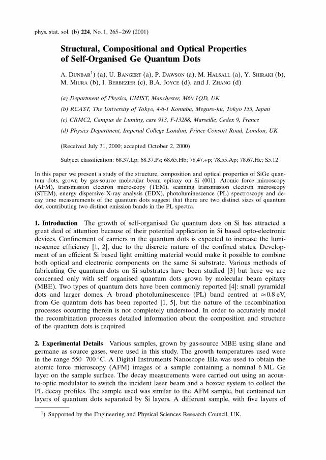
3. Results In the AFM image, shown in Fig. 1, there is a bi-modal distribution of dotsizes, with small pyramidal dots and larger domes. The dot population may be consid-ered as two groups which in this sample have approximately equal densities of1.1 � 109 cm––2. The pyramidal dots have an average basewidth of 45 nm and an aver-age height of 6 nm, whereas the domes have an average basewidth of 94 nm and heightof 18 nm.Both TEM and STEM showed the quantum dots grown in each layer, form on top of
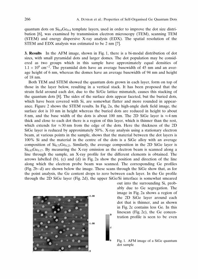
those in the layer below, resulting in a vertical stack. It has been proposed that thestrain field around each dot, due to the Si/Ge lattice mismatch, causes this stacking ofthe quantum dots [8]. The sides of the surface dots appear faceted, but the buried dots,which have been covered with Si, are somewhat flatter and more rounded in appear-ance. Figure 2 shows the STEM results. In Fig. 2a, the high-angle dark field image, thesurface dot is 10 nm in height whereas the buried dots are reduced in height to about8 nm, and the base width of the dots is about 100 nm. The 2D SiGe layer is �4 nmthick and close to each dot there is a region of this layer, which is thinner than the rest,which extends for �30 nm from the edge of the dots. Here the thickness of the 2DSiGe layer is reduced by approximately 50%. X-ray analysis using a stationary electronbeam, at various points in the sample, shows that the material between the dot layers is100% Si and the material in the centre of the dots is a SiGe alloy with an averagecomposition of Si0.75Ge0.25. Similarly, the average composition in the 2D SiGe layer isSi0.83Ge0.17. By measuring the X-ray emission as the electron beam is scanned along aline through the sample, an X-ray profile for the different elements is obtained. Thearrows labelled (b), (c) and (d) in Fig. 2a show the position and direction of the linealong which the electron probe beam was scanned. The corresponding Ge profiles(Fig. 2b–d) are shown below the image. These scans through the SiGe show that, as forthe point analysis, the Ge content drops to zero between each layer. In the Ge profilethrough the 2D SiGe layer (Fig. 2d), the upper SiGe/Si interface is somewhat smeared
out into the surrounding Si, prob-ably due to Ge segregation. Theimage in Fig. 2a shows a region ofthe 2D SiGe layer around eachdot that is thinner, and as shownin Fig. 2c contains less Ge. In thislinescan (Fig. 2c), the Ge concen-tration profile is seen to be even
266 A. Dunbar et al.: Properties of Self-Organised Ge Quantum Dots
Fig. 1. AFM image of a SiGe quantumdot sample
more asymmetric, with the Ge concentra-tion greatest close to the bottom Si/SiGeinterface. The linescan through the centre ofthe dot, Fig. 2b, shows a rather different Geprofile. In this case the greatest Ge concen-tration occurs at the apex of the dot. It ap-pears as though the Ge from the region im-mediately around each dot migrates towardsa nucleation point where it piles up to formthe dot. The existence of a thin region de-pleted of Ge around each dot may play animportant role in the explanation of the op-tical properties of the dots, by providing a
potential barrier separating carriers trapped in the wetting layer from those in thequantum dots.Studying the decay rate of the PL, can help provide a better understanding of the
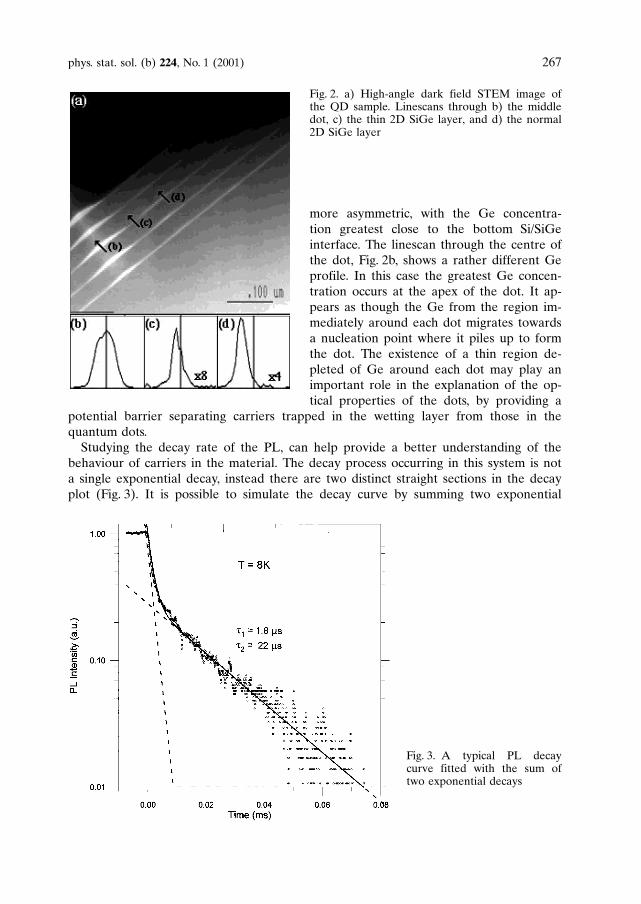
behaviour of carriers in the material. The decay process occurring in this system is nota single exponential decay, instead there are two distinct straight sections in the decayplot (Fig. 3). It is possible to simulate the decay curve by summing two exponential
phys. stat. sol. (b) 224, No. 1 (2001) 267
Fig. 2. a) High-angle dark field STEM image ofthe QD sample. Linescans through b) the middledot, c) the thin 2D SiGe layer, and d) the normal2D SiGe layer
Fig. 3. A typical PL decaycurve fitted with the sum oftwo exponential decays
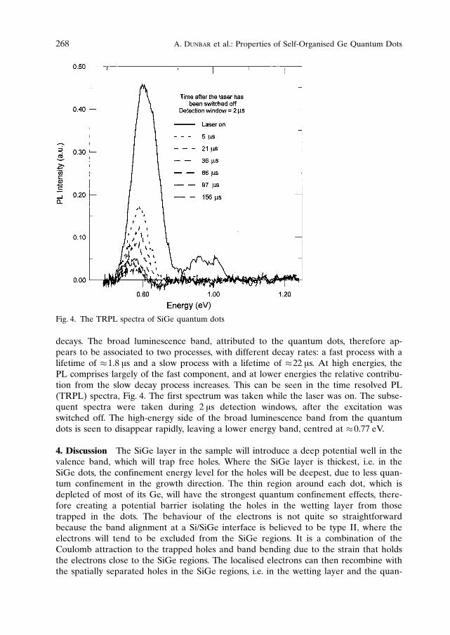
decays. The broad luminescence band, attributed to the quantum dots, therefore ap-pears to be associated to two processes, with different decay rates: a fast process with alifetime of �1.8 ms and a slow process with a lifetime of �22 ms. At high energies, thePL comprises largely of the fast component, and at lower energies the relative contribu-tion from the slow decay process increases. This can be seen in the time resolved PL(TRPL) spectra, Fig. 4. The first spectrum was taken while the laser was on. The subse-quent spectra were taken during 2 ms detection windows, after the excitation wasswitched off. The high-energy side of the broad luminescence band from the quantumdots is seen to disappear rapidly, leaving a lower energy band, centred at �0.77 eV.
4. Discussion The SiGe layer in the sample will introduce a deep potential well in thevalence band, which will trap free holes. Where the SiGe layer is thickest, i.e. in theSiGe dots, the confinement energy level for the holes will be deepest, due to less quan-tum confinement in the growth direction. The thin region around each dot, which isdepleted of most of its Ge, will have the strongest quantum confinement effects, there-fore creating a potential barrier isolating the holes in the wetting layer from thosetrapped in the dots. The behaviour of the electrons is not quite so straightforwardbecause the band alignment at a Si/SiGe interface is believed to be type II, where theelectrons will tend to be excluded from the SiGe regions. It is a combination of theCoulomb attraction to the trapped holes and band bending due to the strain that holdsthe electrons close to the SiGe regions. The localised electrons can then recombine withthe spatially separated holes in the SiGe regions, i.e. in the wetting layer and the quan-
268 A. Dunbar et al.: Properties of Self-Organised Ge Quantum Dots
Fig. 4. The TRPL spectra of SiGe quantum dots
tum dots. The bi-exponential decay rate for the dot luminescence indicates that the PLis coming from two different PL sources, rather than from the no-phonon and TO-pho-non transitions of a single PL source, since all phonon replicas of a PL source have thesame decay rate. It is proposed that the PL comes from the two different types ofquantum dot: pyramids and domes, and the decay rate of each type is different. Thelarge domes produce the PL at 0.75 eV, with a slow decay rate, and the smaller pyra-mids produce the PL at 0.8 eV with a fast decay rate. The domes and pyramids havebeen associated with their respective PL features by assuming that the smaller dotshave greater confinement and therefore they will have a higher PL emission energy.For smaller dots, more hole confinement also suggests a greater likelihood of the holewavefunctions overlapping the wavefunctions of the electrons in the surrounding Si,and therefore a faster decay rate. The converse argument is the case for the largedomes, which have a slower decay rate and emit PL at a lower energy.
References
[1] E. Palange, G. Capellini, L. Di Gaspere, and F. Evangelisti, Appl. Phys. Lett. 68, 86 (1996).[2] T. Takanagahara and K. Takeda, Phys. Rev. B 46, 15578 (1992).[3] Y.S. Tang, C.M. Sotomayor Torres, T.E. Whall, E.H.C. Parker, H. Presting, and H. Kibbel,
J. Mater. Sci. 6, 363 (1995).[4] L. Vescan, T. Stoica, O. Chretien, M. Goryll, E. Mateeva, and A. Muck, J. Appl. Phys. 87,
7275 (2000).[5] H. Sumamura, N. Usami, Y. Shiraki, and S. Fukatsu, Appl. Phys. Lett. 66, 3024 (1995).[6] M. Abdallah, I. Berbezier, P. Dawson, M. Serpentini, G. Bremond, and B. Joyce, Thin Solid
Films 336, 256 (1998).[7] P.D. Siverns, S. Malik, G. McPherson, D. Childs, C. Roberts, R. Murray, and B.A. Joyce, Phys.
Rev. B 58, R10127 (1998).[8] O. Kienzle, F. Ernst, M. Ruhle, O.G. Schmidt, and K. Eberl, Appl. Phys. Lett. 74, 269 (1999).
phys. stat. sol. (b) 224, No. 1 (2001) 269

Recommended