Embed Size (px)
Citation preview

SURFACE MOUNTNOMENCLATUREAND PACKAGING
Tel 800-776-9888 Email [email protected]
w w w . t o p l i n e . t v

Contents
Overview .............................................................................................................................................. 3Flat Chip ............................................................................................................................................... 4MELF Components ..............................................................................................................................10
Tantalum Capacitors .......................................................................................................................... . 12Transistors and Diodes ........................................................................................................................ 14Lead Styles ...........................................................................................................................................20SOIC .................................................................................................................................................... 22TSOP ................................................................................................................................................... 27 PLCC ....................................................................................................................................................28LCC ......................................................................................................................................................29Flat Packs..............................................................................................................................................30QFP ......................................................................................................................................................31BGA (Ball Grid Array) ....................................................................................................................... 36Flip Chips ........................................................................................................................................... 37Micro BGA ......................................................................................................................................... 38Fine Pitch Terminology ...................................................................................................................... 39TopArt ................................................................................................................................................. 42

3
OVERVIEW
This booklet is a plain-English introduction to surface mount nomenclatureand packaging. Soon you will be speaking the language of Surface Mountjust like a professional.
1. Nomenclature
There are many different types of surface mount packages. Each time anew surface mount package is developed a new name is created. Thesenames are usually abbreviated by their initials. As an example: The QuadFlat Pack is commonly known as the QFP. Unfortunately, some packageshave more than one name. This sometimes creates confusion in theindustry. I will do my best to explain the subtle differences betweencomponent types.
2. Package versus Packaging
Let's start by clarifying the difference between the words "package(s)" and"packaging." The word "package" is used in this book to refer to thecomponent's physical shape or outline. The word "packaging" is used inthis book to describe how the component is stored. As an example: Tapeand Reel is the packaging. QFP is a package.
3. Trends
Surface mount technology changes rapidly. However, trends can beidentified. This book includes my observations of industry trends. Byunderstanding these trends, you will gain a fuller appreciation of thecomponents described in this book. They will begin to take on a life of theirown and will become more meaningful to you than just names on a page.

4
FLAT CHIP NOMENCLATURE
Let's start out by studying simple flat chip components such as ceramiccapacitors and resistors.
The footprint (size) of flat chips is identified by a 4-digit size code.
In the USA, this 4-digit size code is measured in inches. Outside the USA,the size code may be either millimeters or inches. This can causeconfusion, so it is important to verify whether the size code is in metric orinches.
The first two digits in the size code refer to the length (L) from Termination-to-Termination. The second two digits refer to the width (W) of thetermination.
For example, if the first two digits in the size code are 12, then the length ofthe flat chip is .12" . However, if the size code is metric, the 12 would equal1.2mm.
The thickness (T) of the package is not included in the 4-digit size code. Youmust refer to the actual manufacturer's data sheet to get informationregarding thickness.
Below are the most common size codes for capacitors and resistors:
Size Code Approximate Size (LxW)
Inch Metric Inch Metric0402 1005* .04" x .02" 1.0 x 0.5mm0504 1210* .05" x .04" 1.2 x 1.0mm0603 1508 .06" x .03" 1.5 x 0.8mm0805 2012 .08" x .05" 2.0 x 1.2mm1005* 2512 .10" x .05" 2.5 x 1.2mm1206 3216 .12" x .06" 3.2 x 1.6mm1210* 3225 .12" x .10" 3.2 x 2.5mm1812 4532 .18" x .12" 4.5 x 3.2mm2225 5664 .22" x .25" 5.6 x 6.4mm
* Caution: Overlapping size codes. Metric appears same as inches.
CONTINUED ON NEXT PAGE

5
FLAT CHIPS
• Capacitors & Resistors
• DimensionsUSA = InchesOutside USA = Metric or Inches
*Thickness is not included
in the 4-digit size code.
12 10Caution: Must verify if size
code is metric or inches.
Example:
Length Width
WL
* T
.12" or 1.2mm .10" or 1.0mm
Terminations
CONTINUED ON NEXT PAGE

6
At the present time, component handling equipment capable of handling0402 size components is not widely available. However, new equipmentcapable of handling small sized components is rapidly being developed.
Small sized components are also more difficult to solder and service in thefield.
In fact, the 0402 is so small, it looks just like a grain of black pepper foundin your kitchen.
Japan is leading the way towards miniaturization. It is still common forAmerican firms to use 1206 and 0805 resistors, while most Japanesecompanies use only 0805 and 0603 sizes. Americans are slowly incorpo-rating 0603 resistors and capacitors into their new designs.
0402 is in the prototype stage in Japan, the USA and Europe.
FLAT CHIP TRENDS
CONTINUED ON NEXT PAGE

7
Prototype
FLAT CHIPS
TRENDS
• Chips Are Getting Smaller
• Japan Leading the WayToward Miniaturization
• Component Handling InfrastructureNot Yet Widely Available for 0402 Size
Design InNow
06030805 0402
1206 0805 0603 0402
USA
Japan
PrototypeNow
CONTINUED ON NEXT PAGE

8
7 inch (178mm) diameter reels are standard around the world for capacitorsand resistors. These reels can hold 5,000 resistors and typically 3,000 to4,000 capacitors.
13 inch (330mm) reels are available on special order for higher volumeusers. The large reel holds more components (example: 10,000 parts) andrequires less handling than do 7 inch (178mm) reels.
Paper (cardboard) reels with punched paper carrier tape are the mostpopular packaging for resistors.
Plastic reels with embossed plastic carrier tape are the most popularpackaging choice for ceramic multilayer capacitors.
Nevertheless, capacitors are available with paper tape and paper reels, andresistors are available with plastic tape and plastic reels.
For low volume assembly, bulk packaging in plastic (vinyl) bags is accept-able.
An alternative type of packaging is now being offered by Japanese firms.Refillable chip shooters (plastic dispensing boxes) and casette holders offerseveral environmental advantages over tape and reel packaging.
Chip shooters consume less physical space and weigh less than tape andreel. Therefore, freight charges (and gas/petrol consumption) are lower.
Since paper tape and paper reels waste trees, refillable chip shootersconserve our forests and natural resources.
Finally, plastic tape and plastic reels are not biodegradeable and this raisesfurther concern over environmental issues.
FLAT CHIP PACKAGING
CONTINUED ON NEXT PAGE

9
PACKAGINGFLAT CHIP
Tape & Reel
7" DIAMETER STANDARD
13" SPECIAL ORDER
Capacitors Resistors1st Choice Plastic 1st Choice Paper2nd Choice Paper 2nd Choice Plastic
CARRIER TAPE
REEL MATERIAL • PLASTIC • PAPER

10
MELF components are more popular in Japan and Europe than in the USA.
MELF stands for Metal Electrode Face Bonded and consists of twoterminals bonded into a cylindrical body.
MELF resistors and capacitors are less expensive than their flat chipcounterparts; however, they require special handling during assembly.
The biggest disadvantage of MELF components is that they may tend to rolloff their solder pads during assembly.
Diodes are also available in MELF and mini-melf packages.
MELF COMPONENTS
CONTINUED ON NEXT PAGE
11
CYLINDRICALMELF
COMPONENTS
• Diodes
• Resistors
• Capacitors
• MELF Not Popular in USA
• Rolls on PC Board
• 0805 • SOD 80 Mini-melf• 1206 1.6mm x 3.5 mm• 1406• 2308 • SM1 Melf
2.5mm x 5.0mm
CapacitorsResistors Diodes

12
Several years ago, the electronic industry adopted the E.I.A. (American)and I.E.C.Q. (European) standard case sizes for molded tantalum capaci-tors.
The Japanese EIAJ standard is not fully compatible with American andEuropean standards.
The E.I.A. and I.E.C.Q. have established four standard case sizes. Thesecase sizes are designated with the letters A, B, C, D or by their 4-digit metricsize code. Package height is not included in the size code.
EIA/IECQ MetricSize Code Code Metric Footprint
A 3216 3.2 X 1.6mmB 3528 3.5 x 2.8mmC 6032 6.0 x 3.2mmD 7343 7.3 x 4.3mm
The most common packaging for molded tantalum capacitors is plastic tapeand either plastic or cardboard reels.
MOLDED TANTALUM CAPACITORS
CONTINUED ON NEXT PAGE

13
MOLDED TANTALUMCAPACITORS
E.I.A. SizesA, B, C, D
Example:
Length Width
3.2 mm 1.6 mm
1632
Footprint is Metric
A case =

14
Rectangular transistors and diodes are SOT packages (Small OutlineTransistor).
The most popular size is the SOT23. Other packages include the SOT89,SOT143 and SOT223.
The Japanese have designated the SC59 which is almost the same size asthe SOT23.
In addition, the Japanese have developed the Mini-SOT which is approxi-mately one-half the size of a standard SOT23.
Motorola developed the DPAK and D2 PAK to house higher-powereddevices. The D2 PAK was designed to replace the popular TO220 leadedtransistor.
TRENDS
Packages for rectangular diodes and transistors are getting both smallerand bigger.
The smallest rectangular transistor is now the mini-SOT, and it is gainingpopularity in Japan.
The biggest surface mount transistor is the D2 PAK which was developedby Motorola to offer a direct footprint equivalent to the popular throughholeTO220 package.
Larger packages are designed to accommodate high power silicon die.
TRANSISTORS AND DIODES
CONTINUED ON NEXT PAGE

15
SOT FEATURES• Rectangular• Easy Placement• Old Technology• SOT 23, SOT 89
SOT 143, SOT 223
DPAK FEATURES• Replaces TO220• High Power• Tape & Reel
SOTTRANSISTORS
AndDIODES
DPAK
SOT 23Most Popular
Mini SOT
CONTINUED ON NEXT PAGE

16
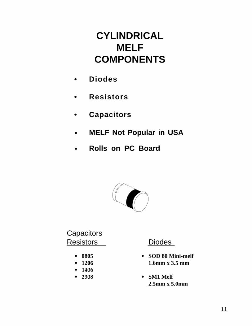
Tape and reel is the most popular packaging for SMD transistors anddiodes. Smaller SOT packages are mounted on 7 inch (178mm) reels.Larger packages such as DPAK and D2 PAK are normally sold on 13 inch(330mm) reels.
Orientation
Caution must be taken in ordering SOT23 with the correct orientation.There are two choices: T1 and T2. The T1 orientation is the most popularand has one lead of the SOT23 facing the sprocket holes on the carrier tape.The T2 is oriented on the tape with two leads facing the sprocket holes.
TRANSISTOR AND DIODE PACKAGING
Typical Quantity on Reel
Package QtySOT23 3,000SOT 89 1,000SOT 143 2,000SOT 223 1,000DPAK 2,500SOD80 2,500SM1 MELF 1,500
Always plasticcarrier tape
CONTINUED ON NEXT PAGE
17
CARRIER TAPE
• Always Plastic
ORIENTATION
• T1 SOT23 1 Lead Toward Sprocket Holes(Most Preferred)
• T2 SOT23 2 Leads Toward Sprocket Holes
TRANSISTOR & DIODE
PACKAGING
• Most Popular T&R
• SOT = 7" Reel
• DPAK = 13" Reel

18
Package types for surface mount integrated circuits can be grouped intofamilies.
The flat pack is old technology.
The QUAD flat pack and TSOP use newer technology.
Each family has certain characteristics in common such as lead style, leadpitch, body size and case materials.
The remainder of this book is devoted to describing SMD integrated circuits.
SMD INTEGRATED CIRCUITS FAMILY
CONTINUED ON NEXT PAGE

19
LEADED CHIPCARRIER
FLAT PACKQUAD FLAT PACK
SMALLOUTLINE
TSOPPIN GRID ARRAY
OVERVIEW
SMDIC FAMILY

20
LEAD STYLES
Let's start by learning the three basic lead styles. Each lead has a namewhich resembles its shape.
Gull-wing leads are small and quite fragile. They can easily be damagedand must be handled with great care.
Gull-wing leads are used to get the highest number of leads onto an IC. Itis possible to get 40 to 80 leads per linear inch (15 to 33 leads per cm) ontoan IC using gull-wing leads. Gull-wing leads are easy to inspect aftersoldering.
J-leads are more sturdy than gull-wing leads; however, they take up morespace. With J-leads, you can only get 20 leads per linear inch (8 leads percm) on an IC package.
Flat leads are also used on IC's. Flat leads must be stored in special carriersto prevent lead damage.
Just prior to use, IC's with flat leads are cut and bent into gull-wings by usinglead forming equipment. Lead forming equipment is an extra expense.Therefore, flat leads are the least popular type of IC lead.
The words lead pitch are synonymous with lead space.
CONTINUED ON NEXT PAGE

21
SMDLEADSSTYLES
•J-LEAD
•GULL-WING
•FLAT

22
SOL
SOLIC
VSOP
SOP
TSOP
?
Small Outline IC's belong to a family of packages with a variety of leadstyles and lead counts. Small outline packages are called by over 10different names. There are small differences between each type, and oftenthey are called by the wrong name. On pages 22 - 23, we will discuss thedifferences.
SOIC SMALL OUTLINE NOMENCLATURE
SO
SSOP
SOJ SOLJ
SOM
CONTINUED ON NEXT PAGE

23
SOIC TRENDS
The trend toward higher density (more leads) continues.
The new VSOP, QSOP and SSOP doubles the number of leads whilemaintaining the traditional small outline appearance. This is accomplishedby decreasing the lead pitch from 50 mils (1.27mm) down to 25 mils (.636mm).
Also, there is a trend to package larger silicon die into wider body SOIC's.This is accomplished by expanding the package width from 300 mils(7.63mm) to 330 mils (8.4mm), 350 mils (8.9mm), 400 mils (10mm) andeven 440 mils (11.1mm).
The TSOP package combines a low profile case with high density lead pitchof 19.7 mils (.5mm). The future looks bright for TSOP packages.
The traditional 150 mil (3.97mm) SO package and 300 mil (7.63mm) SOLpackage are now commonplace in the industry.
CONTINUED ON NEXT PAGE

24
SO Small Outline is the original design. It consists of a molded plastic casemeasuring approximately 156 mils (3.97mm) wide, and has gull-wing leadswith 50 mils (1.27mm) lead pitch.
SOM - Small Outline Medium measures 220 mils (5.6mm) wide. SOMpackages are normally used for resistor networks.
SOL - Small Outline Large measures 300 mils (7.62mm) wide. Widerpackages measuring 330 mils, 350 mils, 400 mils and 450 mils are alsolumped into the SOL family.
SOP - Small Outline Package is a Japanese term which is used the sameway as SO and SOL.
SOJ and SOLJ - Small Outline J-Lead is used to describe SOL packageswith J-leads.
VSOP - Very Small Outline Package refers to packages with high density25 mil (.65mm) gull-wing leads. Sometimes the term VSOP and SSOP (seebelow) are interchangeable. 300 mil (7.62mm) wide body.
SSOP - Shrink Small Outline Package is the same as VSOP; however, ithas a smaller 208 mil (5.3mm) case.
QSOP-Quarter Small Outline Package are the same as the original SOpackage with 25 mil pitch.
Note: The length of the body is determined by the number of leads.
SMALL OUTLINE INTEGRATED CIRCUIT (SOIC)
CONTINUED ON NEXT PAGE

25
SOJ or SOL-J ="J" - Lead Large Outline 300 mil *
SOL = "Large" Outline300 mil
SOP = "Small" Outline Package
8 - 16 PIN
8 - 16 PIN
16 - 32 PIN
16 - 40 PIN
32 - 56 PIN
J-Lead50 mil
GullWing25 mil
BODY LEADDRAWING NOMENCLATURE WIDTH TYPE
SOICSMALL OUTLINEIntegrated Circuit
*Up to 440 mils
SO = Small Outline 156 mil
SSOP = Shrink Small Outline Package 208 mil
GullWing25 mil
VSOP = Very Small Outline Package 300 mil
8 - 30 PIN
20 - 56 PIN
SOM = Medium Outline 220 mil *Gull
50 milPitch
QSOP = Quarter Small Outline Package 156 milGullWing25 mil
CONTINUED ON NEXT PAGE

26
13 inch (330mm) reels are standard for SOIC's. The carrier tape is alwaysplastic and measures 12mm to 32mm in width depending on the IC packagesize.
EXAMPLE OF T&R SOIC PACKAGING
Gull Wing Lead J-LeadPart Qty Tape Part Qty Tape
on Width on WidthReel Reel
S08 2,500 12mm SOLJ16 1,000 16mmSO14 2,500 16mm SOLJ18 1,000 24mmSOM14 2,000 16mm SOLJ20 1,000 24mmSO16 2,500 16mm * SOLJ20/24 1,000 24mmSOM16 2,000 16mm SOLJ24 1,000 24mmSOL16 1,000 16mm SOLJ28 1,000 24mmSOL18 1,000 24mm SOWJ28 500 24mmSOL20 1,000 24mmSOL24 1,000 24mmSOW32 1,000 32mm
SOW = 330 mil wide *20 pin DRAM in 24 lead package
SOIC's are also readily available in plastic tubes. These tubes aresometimes called magazines or sticks.
SOIC PACKAGING
13" STANDARD
TAPE& REEL
TUBE

27
TSOP THIN SMALL OUTLINE PACKAGE
The TSOP (Thin small outline package) combines a low profile package(1.0mm high) with fine-pitch 19.7 mils (.5mm) leads.
The TSOP provides a package which accommodates a large silicon chip ina high density package.
TSOP's are usually shipped in trays; however, tape and reel and tubes areavailable on special request.
The overall dimensions of TSOP's include the leads (total footprint).
TYPE T120 to 56 Lead0.5mm pitch
TYPE T220 Leads
1.27mm pitch

28
PLCC LEADED CHIP CARRIER
• PLCC - Plastic Leaded Chip Carrier
• J-Lead Only
• 18 to 100 Leads
• 50 mil Pitch
• Available in Ceramic Body - CLCC
• Available in Metal Body - MLCC
• Fits Into IC Sockets
• T&R or Tubes
• Trends - PLCC is Common Item No New Development
The plastic body PLCC is the most popular leaded chip carrier. Its J-leadsare always 50 mil (1.27mm) pitch. They are commonly available from 18to 100 leads. PLCC's are usually supplied in tubes or on tape and reel.
As an alternative to the plastic case, leaded chip carriers are available inceramic, known as CLCC, and metal, known as MLCC.
PLCC's fit into IC sockets and can be easily replaced in the field.
PLCC's have been in use for over a decade and are now a common item.

29
LCC LEADLESS CHIP CARRIER
The ceramic LCC is one of the most rugged packages since it has no leadsto damage. LCC's are soldered directly to PC boards by their solder pads,known as castellations. Most LCC's come with 50 mil pitch gold castellationswhich must be pre-coated with solder before mounting.
LCC's are usually designed for Mil Spec, aerospace and high temperatureapplications.
LCC's are shipped in either trays or tubes.
Sometimes LCC's are called LCCC (Leadless Ceramic Chip Carrier).
• LCC
• Solderable Castellation Pads
• 16 Pin to 44 Pin (up to 124 pin)
• Rugged, No Leads to Bend
• Ceramic Body
• High Temp & MilSpec Applications
• Usually Tubes or Trays
30
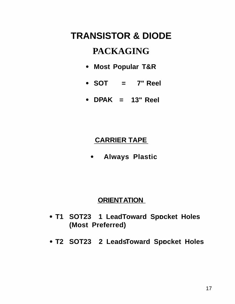
The flat pack is the oldest surface mount IC package.
Since flat packs only are available with 50 mil (1.27mm) lead pitch, theyhave a low lead count such as 14, 16 or 28 leads, though some large flatpacks have up to 80 leads.
Flat packs are used only for Mil Spec, aerospace and other limitedapplications.
Their flat leads must be kept straight in plastic carriers and require leadforming just prior to use. Flat packs usually have gold leads which must bepre-tinned prior to assembly.
It should be noted that flat packs have leads extending from only two sidesof their body. (See quad flat pack for leads extending from four sides.)
FLAT PACKS
• Usually Flat Leads
• 50 mil Pitch
• Must be Formed Prior to Use
• Mil-Spec Applications
• 10 pin to 28 (up to 80)
• Older Technology
• No Significant Trends
• Limited Applications

31
QFP QUAD FLAT PACK
Quad flat packs are high lead count packages.
Quad flat packs are known as fine-pitch devices, since their lead pitch isoften 25.6 mils (.65mm) down to 11.8 mils (.3mm).
The quad flat pack family is available with many options and are called bymany names. See next page for list.
There is still development work going on with quad flat packs.
Lead counts as high as 304 leads are available.
Non-bumpered QFP's are built to Japan's EIAJ metric standard; whereas,bumpered (BQFP's - see page 32) are built to American JEDEC standards.
• EIAJ Standards (Japan)
• No Bumpers
• Gull-Wing
• 44 to 304 leads Now in Production
• .8mm to .3mm Pitch
• Usually Packaged in Trays
• T&R Special Order
CONTINUED ON NEXT PAGE
32
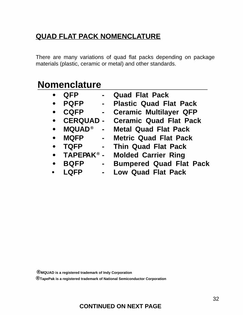
Nomenclature• QFP - Quad Flat Pack• PQFP - Plastic Quad Flat Pack• CQFP - Ceramic Multilayer QFP• CERQUAD - Ceramic Quad Flat Pack• MQUAD ® - Metal Quad Flat Pack• MQFP - Metric Quad Flat Pack• TQFP - Thin Quad Flat Pack• TAPEPAK ® - Molded Carrier Ring• BQFP - Bumpered Quad Flat Pack• LQFP - Low Quad Flat Pack
There are many variations of quad flat packs depending on packagematerials (plastic, ceramic or metal) and other standards.
QUAD FLAT PACK NOMENCLATURE
®TapePak is a registered trademark of National Semiconductor Corporation
®MQUAD is a registered trademark of Indy Corporation
CONTINUED ON NEXT PAGE

33
NOMENCLATUREQUAD FLAT PACKS
MQUAD®
CQFP
QFP
TAPEPAK ®
CERQUAD
MQFP
PQFP
TQFP
LQFPBQFP
?

34
The bumpered quad flat pack is built to American JEDEC standards usingtrue inch measurements. This means that 25 mil lead pitch is truly 25 mils(.636mm not .65mm).
The purpose of the bumpered corners is to protect the leads duringshipping, handling and assembly.
BQFP's are constructed in a plastic package; however, they are alsoavailable with metal case, known as the BMQUAD.
BQFP's always have gull-wing leads and are shipped in trays, tubes or ontape and reel.
BQFP BUMPERED QUAD FLA T PACK
• JEDEC Standard (USA)
• Bumpered Corners - Protects Leads
• Gull-Wing
• Up to 196 Leads
• Package Options - Trays, Tubes and T&R
• True 25 mil (.636mm) Pitch

35
TapePak® was invented by National Semiconductor and is now licensedfor production by several manufacturers.
Known for its molded carrier ring, the leads remain safe from damage. Themolded carrier ring allows the device to be tested before the need to cut andform the leads.
Leads up to 304 are now available with TapePak.®
The main disadvantage with TapePak® is the added expense to providelead forming equipment.
TAPEPAK® Molded Carrier Ring
• Molded Carrier RingKeeps Leads Flat Prior to Use
• Allows Automated Testing
• 120 pins to 304 pins
• 25mil to 15.7mil Pitch
• 0.65mm to 0.4mm Pitch
• Coin Stack in Tubes
• Requires Lead FormingEquipment
®TapePak is a registered trademark of National Semiconductor .

37
Flip chips are bare die with small solder bumps on the bottom whichserve as "leads."
The flip chip is soldered directly to a PC Board (FR4 or ceramic) byplacing the component on the board and applying heat. The solderbumps melt to corresponding pads on the PC Board.
The following solder type (Eutectic) is used for the bumps:
FR4 Boards 63% - 37% low melt (183ºC)Ceramic Boards: 95% - 5% requires high temp
Bump on the die are around the perimeter and also in the middle.
Since the parts are small, dimensions are specified in "microns" notmillimeters.
100µm = 1 millimeter
Important Package Specifiers:
A. Die SizeB. Number BumpsC. Diameter of BumpsD. Solder Composition of BumpsE. Bump Pitch
FLIP CHIPS
39
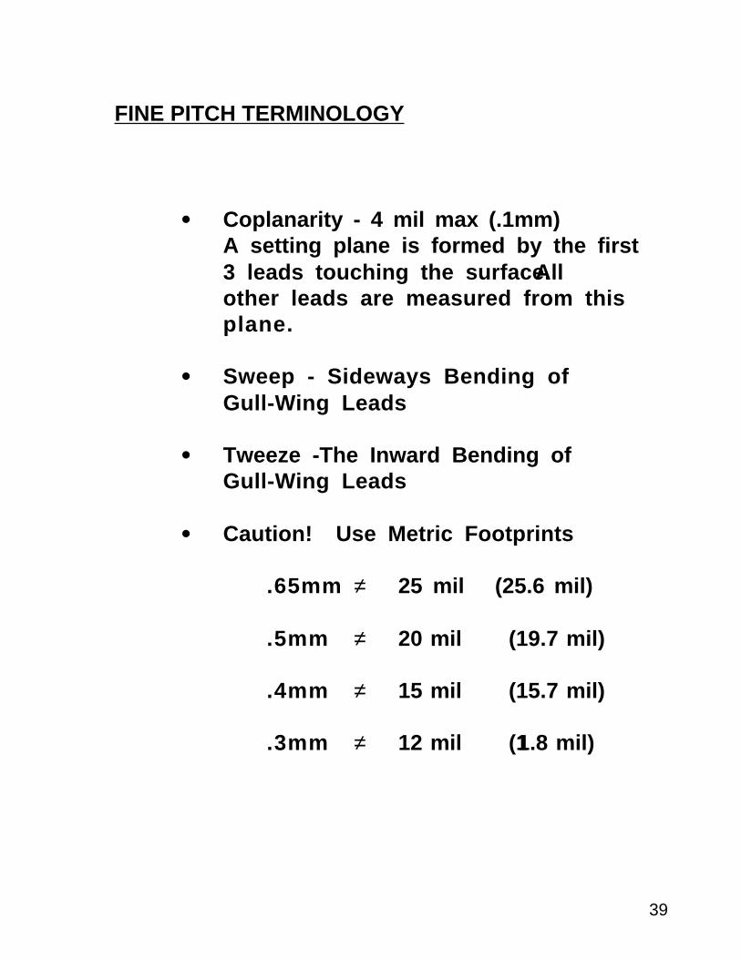
• Coplanarity - 4 mil max (.1mm)A setting plane is formed by the first3 leads touching the surface. Allother leads are measured from thisplane.
• Sweep - Sideways Bending ofGull-Wing Leads
• Tweeze - The Inward Bending ofGull-Wing Leads
• Caution! Use Metric Footprints
.65mm ≠ 25 mil (25.6 mil)
.5mm ≠ 20 mil (19.7 mil)
.4mm ≠ 15 mil (15.7 mil)
.3mm ≠ 12 mil (11.8 mil)
FINE PITCH TERMINOLOGY

41
TopLine, with their Solder Practice Kits, makes practicing with the latest technologicaladvancements accessible and affordable. These three popular kits are designed frombeginners to advanced practice. The BGA kit supports 4 BGAs, with 1.5mm grid pat-tern, and daisy chain test points to verify placement. The 88-piece Challenger Kit in-cludes a wide selection of SMD components, including fine pitch QFP, PLCC, SOIC,LCC and discrete components. The Advanced Rework Kit was designed especially forhand-solder or machine run. Solder paste artwork, parts placement data and solderpaste stencils are also available.
Solder Practice KitsFa
x 1-
310-
498-
0490
©
199
3 To
pLin
e
Ph
1-31
0-43
3-70
00
Ball Grid Array
PN
9670
01 T1+ T2+ T3+ T4+ T5+
T1- T2- T3- T4- T5-
Ball 15Ball 1
BGA2251.5mm Pitch
T1+ T2+ T3+ T4+ T5+
T1- T2- T3- T4- T5-
Ball 15Ball 1
Ball 13
Ball 1
BGA2251.5mm Pitch
BGA1691.5mm Pitch
Ball 13
Ball 1
BGA1691.5mm Pitch
T1+
T1-
T2+ T3+ T4+ T5+ T6+ T7+
T2- T3- T4- T5- T6- T7-
T1+
T1-
T2+ T3+ T4+ T5+ T6+ T7+
T2- T3- T4- T5- T6- T7-
TM
11751 Markon Drive
Garden Grove
California
92841
USA
Tel : 1-714-898-3830
Fax : 1-714-891-0321
TopLine is the world's leading supplier of Dummy Components. Inaddition, TopLine offers Solder Practice Kits, SMD Hand Tools andSoftware Packages. With a vast network of distributors spanning 23countries worldwide, TopLine supports pick and placemanufacturers, educational institutions, as well as many otherrapidly expanding markets. Customer service is of the utmostimportance at TopLine. That's why we guarantee the quality of ourproducts. Call today to receive your free TopLine catalog.
TM
Fax
1-31
0-49
8-04
90
© 1
993
TopL
ine
P
h 1-
310-
433-
7000
Challenger Kit
PN
9200
01
SOL 20
SOLJ 24
CRYSTAL
LCC 40
0805
1206
MELF
MINI MELF 0603
1210
0402
1210
Inductor
1812
Tantalum
A
B C
D
1812 2225Pot.
SOM 16SO 14PLCC 20
SOT 23
BQFP132 25Mil
QFP84 .8mm
AL CAP
6.3mm 4mm
SOT 89
SOT 223
SOT 143 D PAK
PLCC 68 QFP184 .65mm QFP52 1mm
1008 Inductor
Rework Practice
Fax
1-31
0-49
8-04
90
© 1
993
TopL
ine
Ph
1-31
0-43
3-70
00
SOL 20
PLCC 68
PLCC 20
SO 14
1206 (3216)
PN
965
001
PLCC 44PLCC 20
SOM 16
SO 14
SOT 23
BQFP 132
QFP 208
TSOP 32
QFP100
0805 (2012)
PLCC 44
Order Number Description967000 Ball Grid Array920025 Challenger Kit965000 Advanced Challenger Kit