Embed Size (px)
Citation preview
Nati
on
al In
sti
tute
of
Scie
nce &
Te
ch
nolo
gy
[1]
Cadence Design Contest –2015
Presented By: Rajib & Susmita
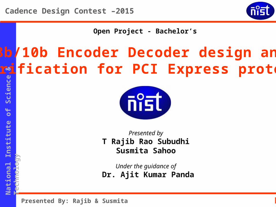
8b/10b Encoder Decoder design and Verification for PCI Express protocol
Open Project - Bachelor’s
Presented by
T Rajib Rao SubudhiSusmita Sahoo
Under the guidance of
Dr. Ajit Kumar Panda
Nati
on
al In
sti
tute
of
Scie
nce &
Te
ch
nolo
gy
[2]
Cadence Design Contest –2015
Presented By: Rajib & Susmita
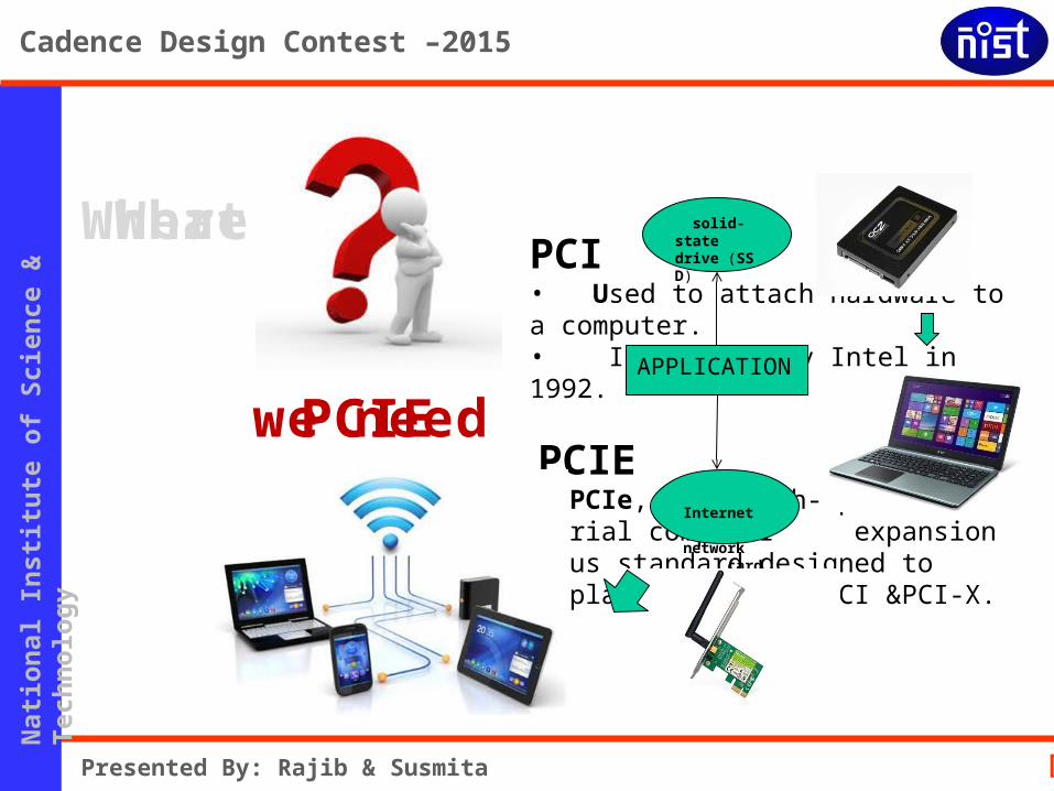
What
PCI
PCI• Used to attach hardware to a computer.• Introduced by Intel in 1992.
PCIE PCIE• PCIe, is a high-speed serial computer expansion bus standard designed to replace the older PCI &PCI-X.
Where
we needAPPLICATION
solid-state drive (SSD)
Internet network card
Nati
on
al In
sti
tute
of
Scie
nce &
Te
ch
nolo
gy
[3]
Cadence Design Contest –2015
Presented By: Rajib & Susmita
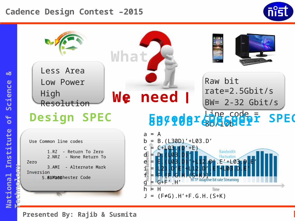
WhatLess AreaLow PowerHigh Resolution
Raw bit rate=2.5Gbit/sBW= 2-32 Gbit/sLine code = 8b/10bEncoder/Decoder SPECDesign SPEC
we need
What
We need
a = Ab = B.(L30D)’+L03.D’c = C+L03.(D’+E)d = D.(L03.D)’e = E.(L03.D)’+L12.D’.E’+L03.D.E’i = L21.D’E’+L12.D’.E’+L03.D.E’f = F.[F.G.H.(S+K)]’g = G+F’.H’h = HJ = (F≠G).H’+F.G.H.(S+K)
8B/10B encoder Use Common line codes
1.RZ - Return To Zero 2.NRZ - None Return To Zero 3.AMI - Alternate Mark Inversion 4.Manchester Code
5.8B/10B
Nati
on
al In
sti
tute
of
Scie
nce &
Te
ch
nolo
gy
[4]
Cadence Design Contest –2015
Presented By: Rajib & Susmita
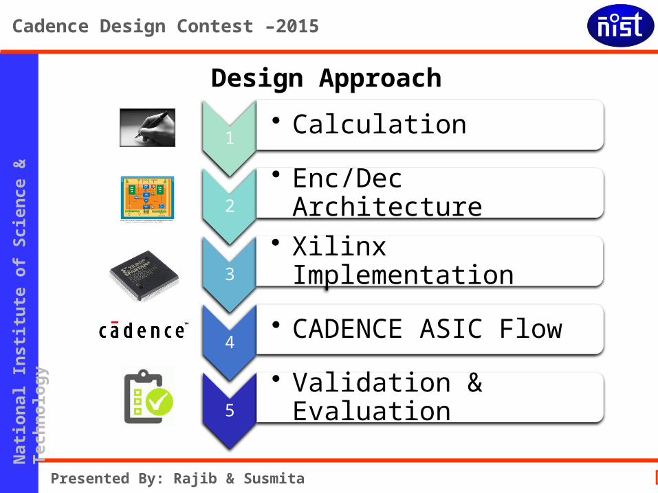
1• Calculation
2• Enc/Dec Architecture
3• Xilinx Implementation
4• CADENCE ASIC Flow
5
• Validation & Evaluation
Design Approach
Nati
on
al In
sti
tute
of
Scie
nce &
Te
ch
nolo
gy
[5]
Cadence Design Contest –2015
Presented By: Rajib & Susmita
5b/6bencoding
3b/4bencoding
control
DisparityGeneration
D_FF
D_FF
D_FF
D_FF
D_FFxor
xor
Datain_8b [7:0]
Encoder
kin
rdispin
K_error
rdispout
Dataout_10b [9:0]
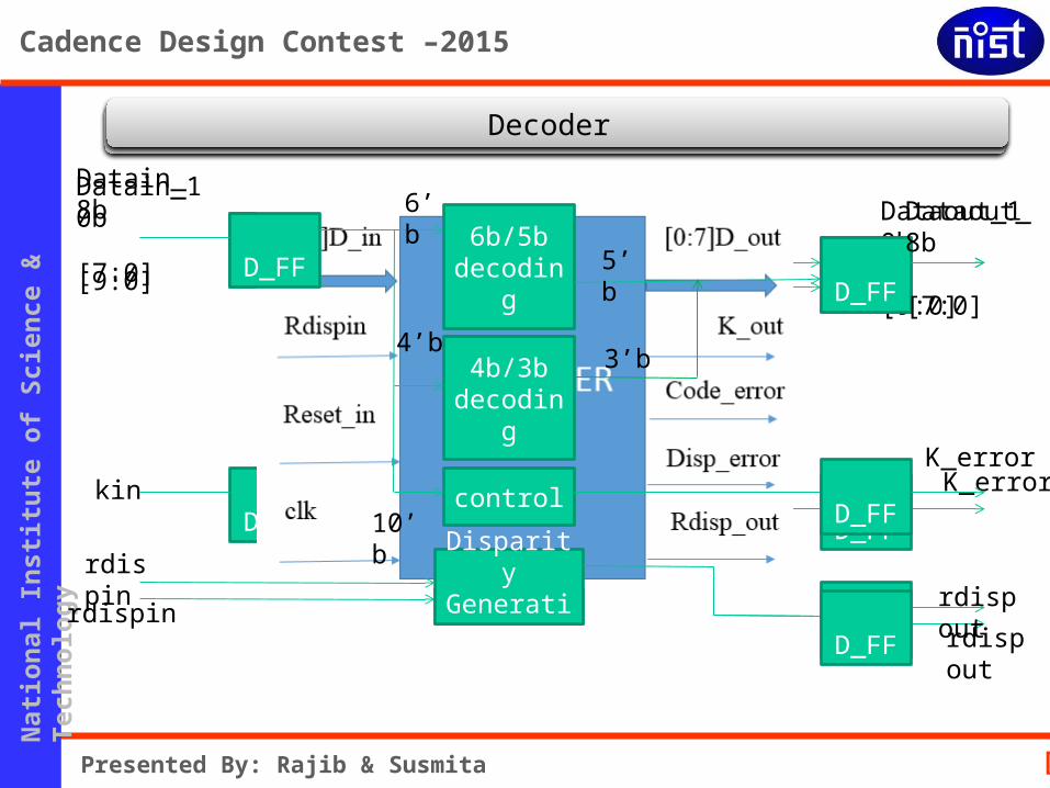
Decoder
6b/5bdecoding
4b/3bdecoding
control
DisparityGeneration
D_FF
D_FF
D_FF
D_FF
Datain_10b [9:0]
6’b
4’b
10’b
rdispinrdispout
5’b
3’b
K_error
Dataout_8b [7:0]
Nati
on
al In
sti
tute
of
Scie
nce &
Te
ch
nolo
gy
[6]
Cadence Design Contest –2015
Presented By: Rajib & Susmita
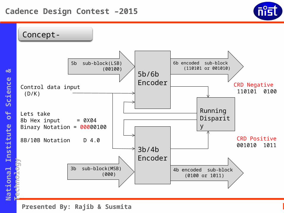
5b/6bEncoder
3b/4bEncoder
RunningDisparity
5b sub-block(LSB) (00100)
Control data input (D/K)
Lets take8b Hex input = 0X04Binary Notation = 00000100
8B/10B Notation D 4.0
3b sub-block(MSB) (000)
4b encoded sub-block (0100 or 1011)
6b encoded sub-block (110101 or 001010)
CRD Negative 110101 0100
CRD Positive001010 1011
Concept-
Nati
on
al In
sti
tute
of
Scie
nce &
Te
ch
nolo
gy
[7]
Cadence Design Contest –2015
Presented By: Rajib & Susmita
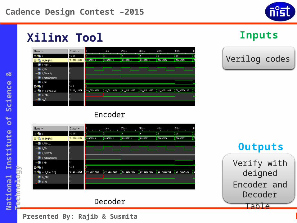
Verilog codes
Verify with deigned
Encoder and Decoder
Table
Inputs
Outputs
Xilinx Tool
Encoder
Decoder
Nati
on
al In
sti
tute
of
Scie
nce &
Te
ch
nolo
gy
[8]
Cadence Design Contest –2015
Presented By: Rajib & Susmita
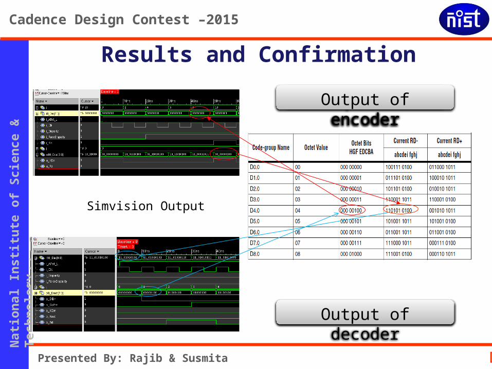
Results and Confirmation
Input of decoderOutput of decoder
Input to encoderOutput of encoder
Simvision Output
Nati
on
al In
sti
tute
of
Scie
nce &
Te
ch
nolo
gy
[9]
Cadence Design Contest –2015
Presented By: Rajib & Susmita
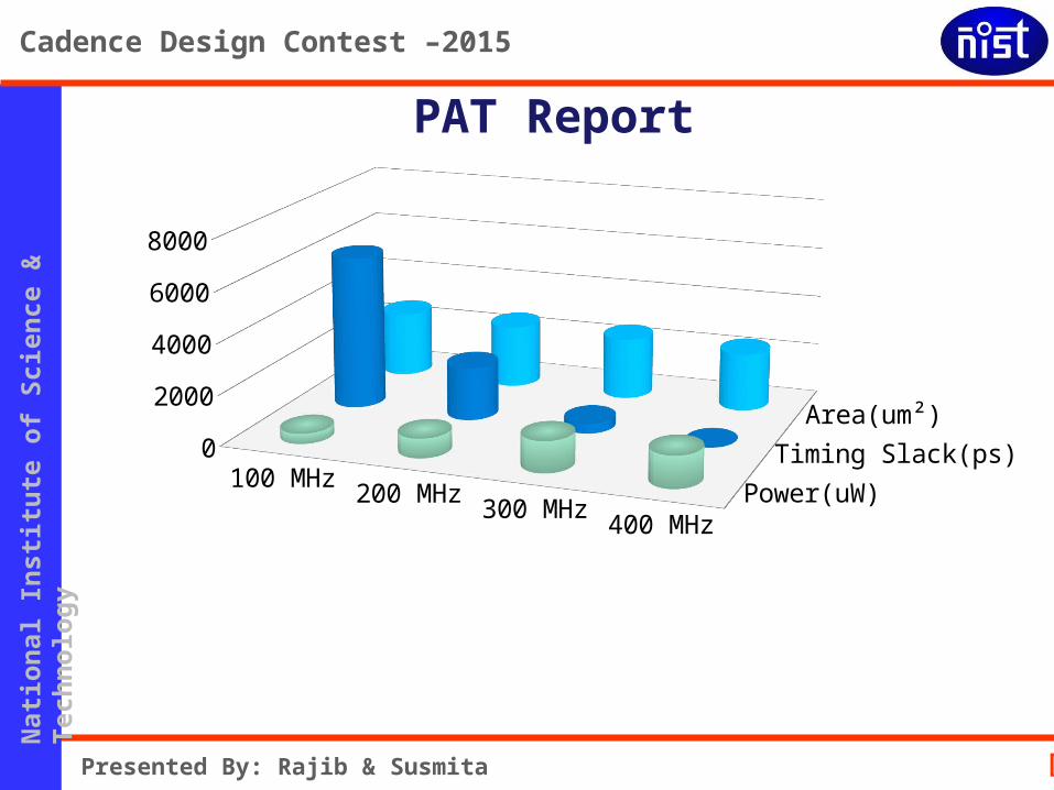
PAT Report
100 MHz 200 MHz 300 MHz 400 MHz
Power(uW)
406.09 770.685 1235.789 1257.176
Tim-ing Slack(ps)
6097 2108 396 1.8
Area(um²)
2591 2498 2435 2302
500150025003500450055006500
Power(uW)
Timing Slack(ps)
Area(um²)
Nati
on
al In
sti
tute
of
Scie
nce &
Te
ch
nolo
gy
[10]
Cadence Design Contest –2015
Presented By: Rajib & Susmita
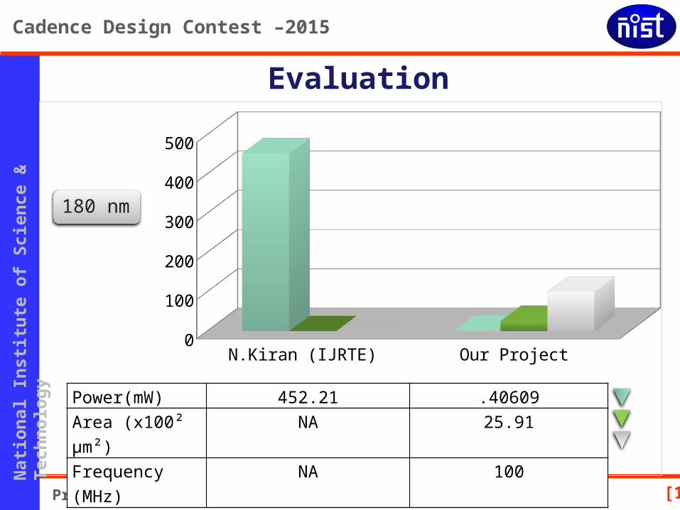
Evaluation
180 nm
N.Kiran (IJRTE) Our Project
Power(mW) 452.21 0.40609
Area (x100² µm²) 0 25.91
Frequency (MHz) 0 100
2575
125175225275325375425475
Power(mW) 452.21 .40609Area (x100² µm²) NA 25.91Frequency (MHz) NA 100
Nati
on
al In
sti
tute
of
Scie
nce &
Te
ch
nolo
gy
[11]
Cadence Design Contest –2015
Presented By: Rajib & Susmita
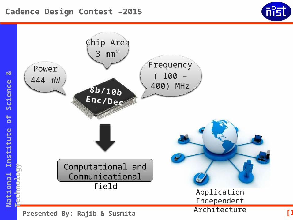
8b/10bEnc/Dec
Power444 mW
Chip Area3 mm²
Frequency( 100 – 400)
MHz
Computational and Communicational
fieldApplication Independent
Architecture
Nati
on
al In
sti
tute
of
Scie
nce &
Te
ch
nolo
gy
[12]
Cadence Design Contest –2015
Presented By: Rajib & Susmita
Nati
on
al In
sti
tute
of
Scie
nce &
Te
ch
nolo
gy
[13]
Cadence Design Contest –2015
Presented By: Rajib & Susmita
• “Design of Physical Coding Sublayer using 8B/10B Algorithm” N.Kiran Babu, P.S.Srinivas Babu, International Journal of Recent Technology and Engineering (IJRTE) ISSN: 2277-3878, May 2013
• “8B/10B Encoding And Decoding For High Speed Applications” Alber X.Widmer, IBM Reserch Report RC23408 (W0411-032) November 3,2010.
Reference


![[DL輪読会]Encoder-Decoder with Atrous Separable Convolution for Semantic Image Segmentation](https://img.pdfslide.tips/doc/110x75/5aaa85d17f8b9af9198b4679/dlencoder-decoder-with-atrous-separable-convolution-for-semantic.jpg)