Embed Size (px)
Citation preview
Prof. Snehal Laddha
Optical sources 2:
The light-emitting diode
Prof. Snehal Laddha
The normally empty conduction band of the semiconductor is populated by electrons injected into it by the forward current through the junction, and light is generated when these electrons recombine with holes in the valence band to emit a photon.
This is the mechanism by which light is emitted from an LED
PRINCIPLE
Prof. Snehal Laddha
Simpler fabrication. There are no mirror facets and in some structures no striped geometry.
Cost. The simpler construction of the LED leads to much reduced cost which is always likely to be maintained.
Reliability. The LED does not exhibit catastrophic degradation and has proved far less sensitive to gradual degradation than the injection laser. It is also immune to self-pulsation and modal noise problems.
Generally less temperature dependence. The light output against current characteristic is less affected by temperature than the corresponding characteristic for the injection laser. Furthermore, the LED is not a threshold device and therefore raising the temperature does not increase the threshold current above the operating point and hence halt operation.
Simpler drive circuitry. This is due to the generally lower drive currents and reduced temperature dependence which makes temperature compensation circuits unnecessary.
Linearity. Ideally, the LED has a linear light output against current characteristic unlike the injection laser. This can prove advantageous where analog modulation is concerned.
ADVANTAGES

Prof. Snehal Laddha
Generally lower optical power coupled into a fiber (microwatts);
usually lower modulation bandwidth; harmonic distortion.
Drawbacks

Prof. Snehal Laddha
Led power and efficiency numericals
Prof. Snehal Laddha
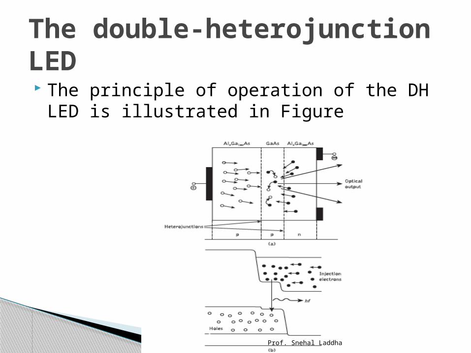
The principle of operation of the DH LED is illustrated in Figure
The double-heterojunction LED
Prof. Snehal Laddha
The device shown consists of a p-type GaAs layer sandwiched between a p-type AlGaAs and an n-type AlGaAs layer.
When a forward bias is applied (as indicated in Figure (a), electrons from the n-type layer are injected through the p–n junction into the p-type GaAs layer where they become minority carriers.
These minority carriers diffuse away from the junction, recombining with majority carriers (holes) as they do so. Photons are therefore produced with energy corresponding to the bandgap energy of the p-type GaAs layer.
Prof. Snehal Laddha
The injected electrons are inhibited from diffusing into the p-type AlGaAs layer because of the potential barrier presented by the p–p heterojunction (Figure (b)).
Hence, electroluminescence only occurs in the GaAs junction layer, providing both good internal quantum efficiency and high-radiance emission.
Furthermore, light is emitted from the device without reabsorption because the bandgap energy in the AlGaAs layer is large in comparison with that in GaAs.
Prof. Snehal Laddha
The DH structure is therefore used to provide the most efficient incoherent sources for application within optical fiber communications.
Nevertheless, these devices generally exhibit the previously discussed constraints in relation to coupling efficiency to optical fibers.

Prof. Snehal Laddha
There are six major types of LED structure and although only two have found extensive use in optical fiber communications, two others have become increasingly applied.
These are the surface emitter, the edge emitter, the superluminescent and the resonant cavity LED respectively.
The other two structures, the planar and dome LEDs, find more application as cheap plastic-encapsulated visible devices for use in such areas as intruder alarms, TV channel changers and industrial counting.
However, infrared versions of these devices have been used in optical communications mainly with fiber bundles and it is therefore useful to consider them briefly before progressing to the high-radiance LED structures.
LED structures
Prof. Snehal Laddha
Planar LED
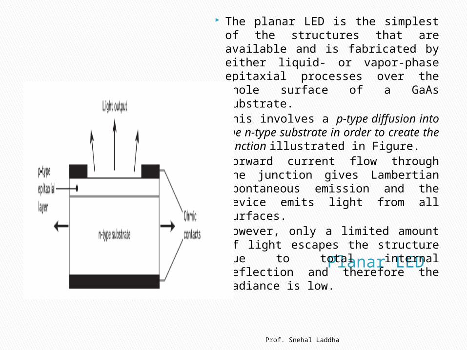
The planar LED is the simplest of the structures that are available and is fabricated by either liquid- or vapor-phase epitaxial processes over the whole surface of a GaAs substrate.
This involves a p-type diffusion into the n-type substrate in order to create the junction illustrated in Figure.
Forward current flow through the junction gives Lambertian spontaneous emission and the device emits light from all surfaces.
However, only a limited amount of light escapes the structure due to total internal reflection and therefore the radiance is low.
Prof. Snehal Laddha
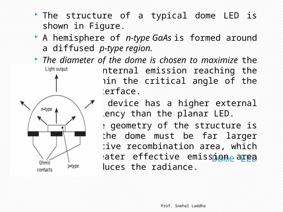
Dome LED
The structure of a typical dome LED is shown in Figure.
A hemisphere of n-type GaAs is formed around a diffused p-type region.
The diameter of the dome is chosen to maximize the amount of internal emission reaching the surface within the critical angle of the GaAs–air interface.
Hence this device has a higher external power efficiency than the planar LED.
However, the geometry of the structure is such that the dome must be far larger than the active recombination area, which gives a greater effective emission area and thus reduces the radiance.
Prof. Snehal Laddha
A method for obtaining high radiance is to restrict the emission to a small active region within the device.
These structures have a low thermal impedance in the active region allowing high current densities and giving high-radiance emission into the optical fiber.
Surface emitter LEDs
Prof. Snehal Laddha
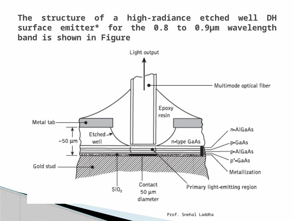
The structure of a high-radiance etched well DH surface emitter* for the 0.8 to 0.9μm wavelength band is shown in Figure
Prof. Snehal Laddha
The internal absorption in this device is very low due to the larger bandgap-confining layers, and the reflection coefficient at the back crystal face is high giving good forward radiance.
The emission from the active layer is essentially isotropic, although the external emission distribution may be considered Lambertian with a beam width of 120° due to refraction from a high to a low refractive index at the GaAs–fiber interface.
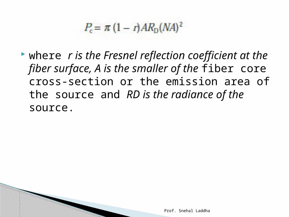
The power coupled Pc into a multimode step index fiber may be estimated from the relationship
Prof. Snehal Laddha
where r is the Fresnel reflection coefficient at the fiber surface, A is the smaller of the fiber core cross-section or the emission area of the source and RD is the radiance of the source.

Prof. Snehal Laddha

Prof. Snehal Laddha
Stripe geometry DH edge emitter LED (ELED)
Edge emitter LEDs
Prof. Snehal Laddha
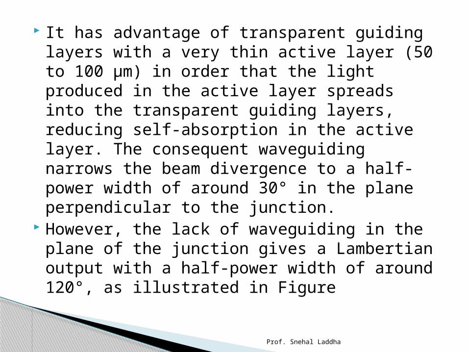
It has advantage of transparent guiding layers with a very thin active layer (50 to 100 μm) in order that the light produced in the active layer spreads into the transparent guiding layers, reducing self-absorption in the active layer. The consequent waveguiding narrows the beam divergence to a half-power width of around 30° in the plane perpendicular to the junction.
However, the lack of waveguiding in the plane of the junction gives a Lambertian output with a half-power width of around 120°, as illustrated in Figure
Prof. Snehal Laddha
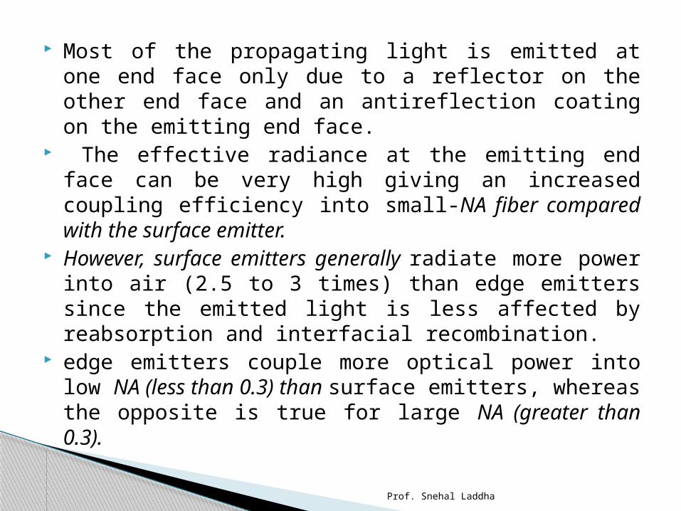
Most of the propagating light is emitted at one end face only due to a reflector on the other end face and an antireflection coating on the emitting end face.
The effective radiance at the emitting end face can be very high giving an increased coupling efficiency into small-NA fiber compared with the surface emitter.
However, surface emitters generally radiate more power into air (2.5 to 3 times) than edge emitters since the emitted light is less affected by reabsorption and interfacial recombination.
edge emitters couple more optical power into low NA (less than 0.3) than surface emitters, whereas the opposite is true for large NA (greater than 0.3).
Prof. Snehal Laddha
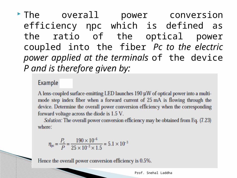
The overall power conversion efficiency ηpc which is defined as the ratio of the optical power coupled into the fiber Pc to the electric power applied at the terminals of the device P and is therefore given by: