Embed Size (px)
Citation preview
Beyond 20% efficiency n-type solar cells
Arthur Weeber
www.ecn.nl
Thanks to:
Ingrid Romijn, Teun Burgers, Bart Geerligs, Anna Carr, Astrid Gutjahr, Desislava Saynova, Jan Bultman, Benoit Heurtault, Bas van Aken, Mark Jansen, Nicolas Guillevin, Loek Berkeveld, John Anker and Martien Koppes
Lang Fang, Xiong Jingfeng, Li Gaofei, Xu Zhuo, Wang Lang Fang, Xiong Jingfeng, Li Gaofei, Xu Zhuo, Wang Hongfang, Hu Zhiyang, Zhao Wenchao, Wang Jianming, Wang Ziqian, Chen Yingle, Shen Yanlong, Chen Jianhui, Yu Bo, Tian Shuquan
Peter Venema, Ard Vlooswijk
2 25-4-2012
Why n-type?
• Absence of boron-oxygen complexes- No light induced degradation in n-type Cz material
• Less sensitive to common impurities- Higher diffusion length in n-type
3 25-4-2012
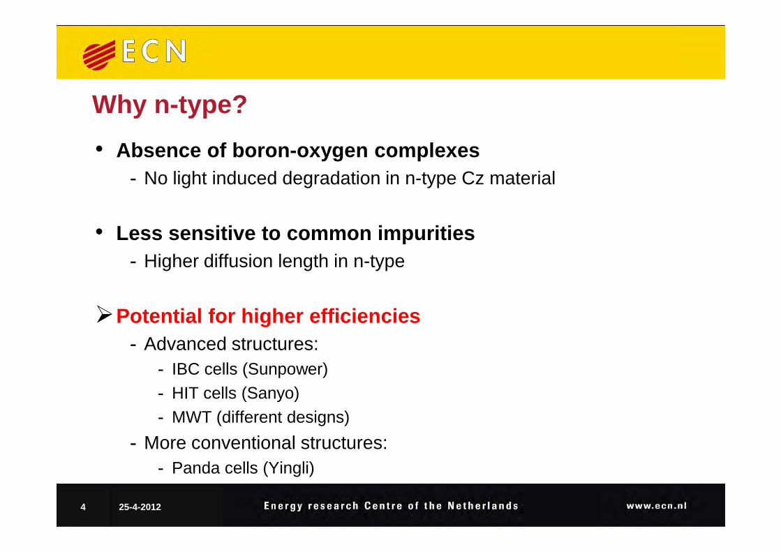
Why n-type?
• Absence of boron-oxygen complexes- No light induced degradation in n-type Cz material
• Less sensitive to common impurities- Higher diffusion length in n-type
Potential for higher efficiencies - Advanced structures:
- IBC cells (Sunpower) - HIT cells (Sanyo)- MWT (different designs)
- More conventional structures: - Panda cells (Yingli)
4 25-4-2012
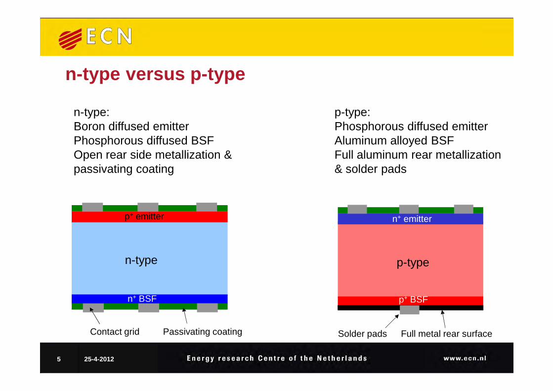
n-type versus p-type
n-type:Boron diffused emitterPhosphorous diffused BSFOpen rear side metallization & passivating coating
p-type:Phosphorous diffused emitterAluminum alloyed BSFFull aluminum rear metallization & solder pads
5 25-4-2012
n-type
n+ BSF
p+ emitter
Contact grid Passivating coating
p-type
p+ BSF
n+ emitter
Solder pads Full metal rear surface
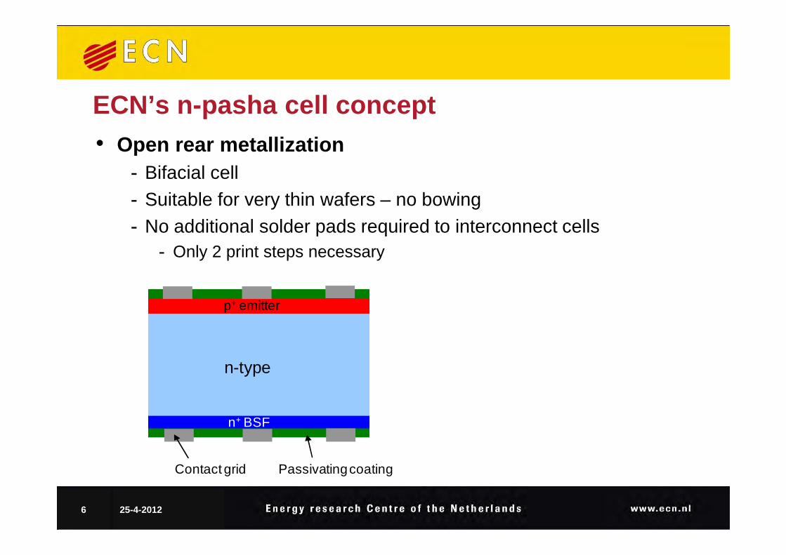
ECN’s n-pasha cell concept• Open rear metallization
- Bifacial cell- Suitable for very thin wafers – no bowing- No additional solder pads required to interconnect cells
- Only 2 print steps necessary
6 25-4-2012
n-type
n+ BSF
p+ emitter
Contact grid Passivating coating
ECN’s n-pasha cell concept• Open rear metallization
- Bifacial cell- Suitable for very thin wafers – no bowing- No additional solder pads required to interconnect cells
- Only 2 print steps necessary
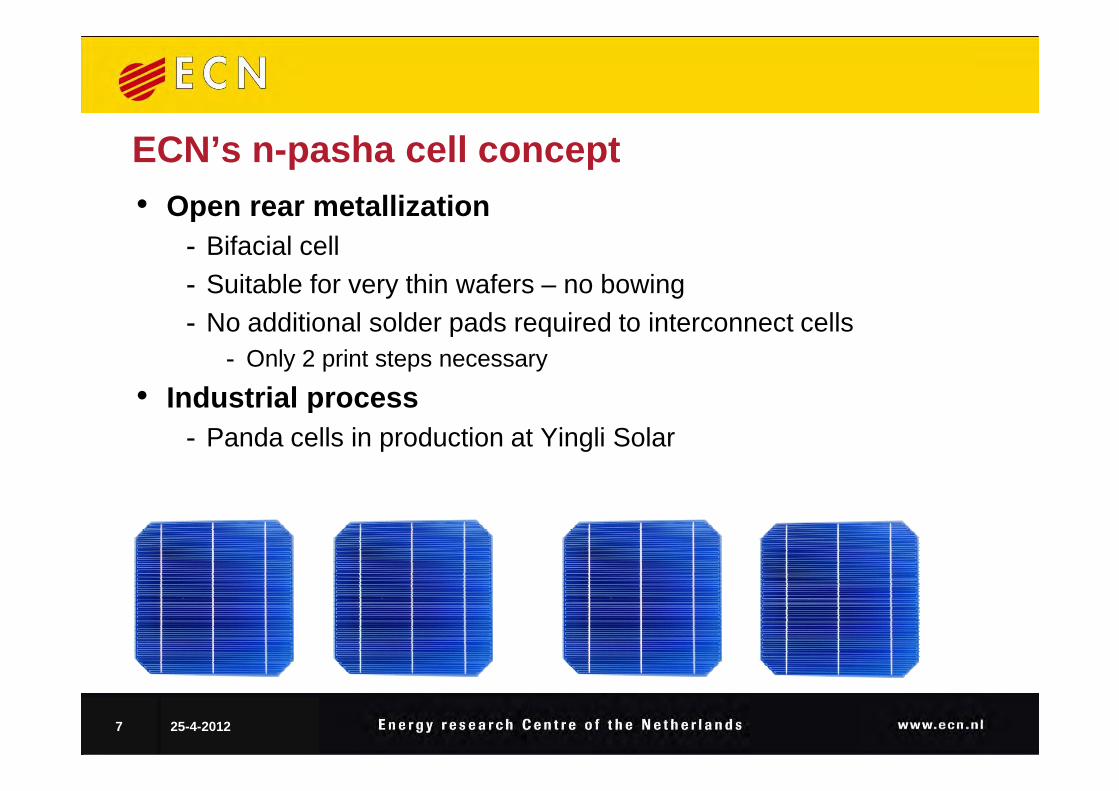
• Industrial process
7 25-4-2012
• Industrial process- Panda cells in production at Yingli Solar
Recent progress on n-pasha
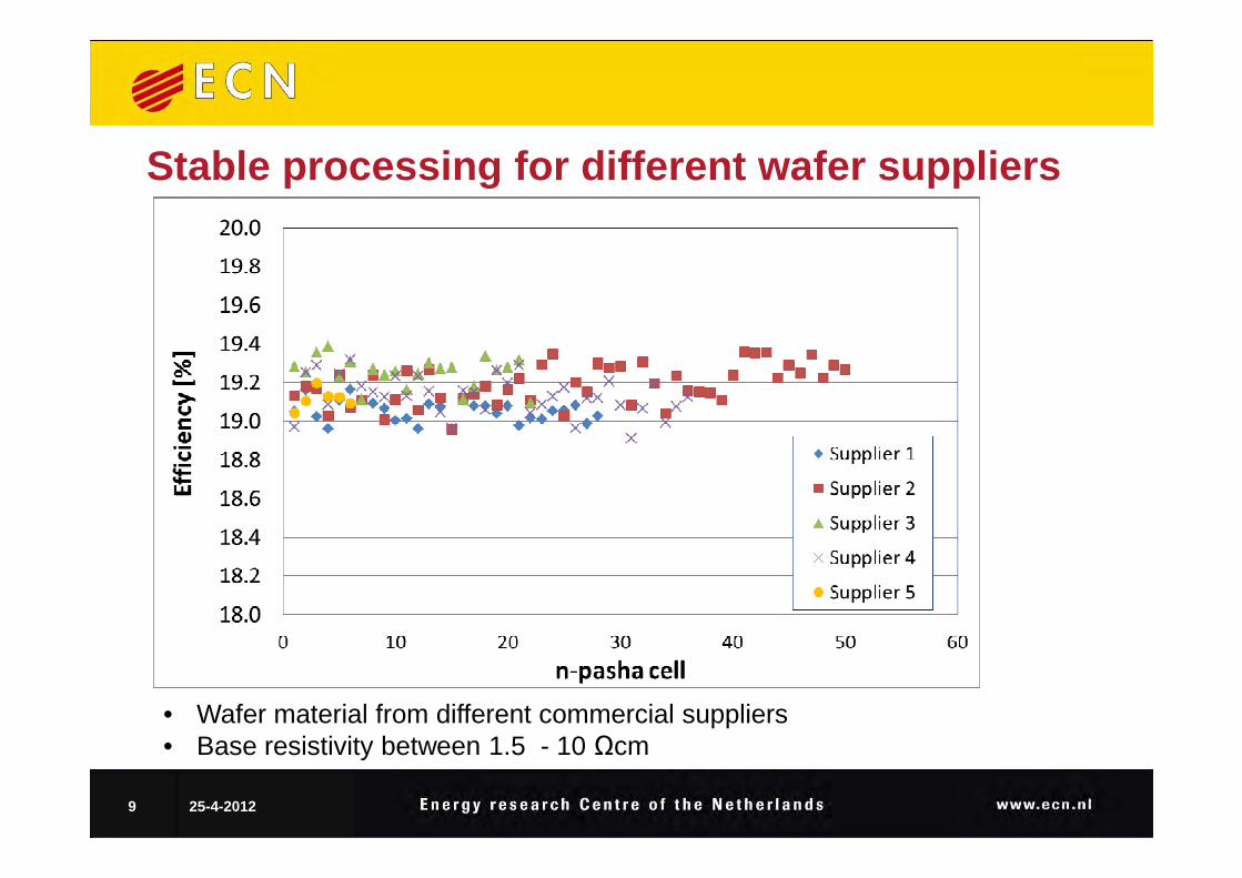
Stable processing for different wafer suppliers
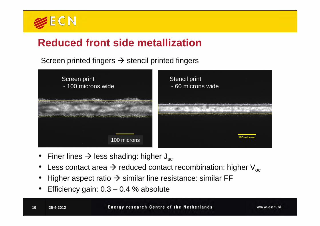
Reduced front side metallization
Improved rear surface passivation Improved rear surface passivation
8 25-4-2012
Stable processing for different wafer suppliers
9 25-4-2012
• Wafer material from different commercial suppliers• Base resistivity between 1.5 - 10 Ωcm
Reduced front side metallization
Screen print~ 100 microns wide
Stencil print~ 60 microns wide
Screen printed fingers stencil printed fingers
• Finer lines less shading: higher Jsc
• Less contact area reduced contact recombination: higher Voc
• Higher aspect ratio similar line resistance: similar FF• Efficiency gain: 0.3 – 0.4 % absolute
10 25-4-2012
100 microns
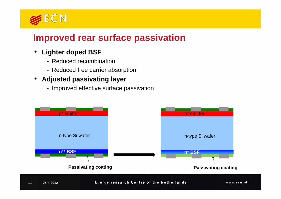
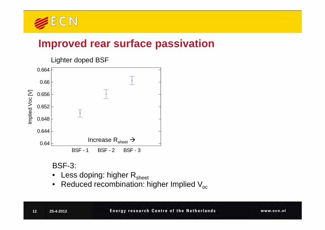
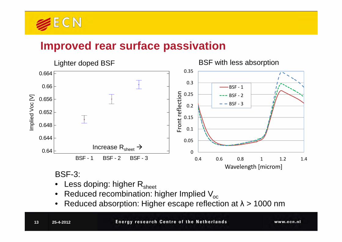
Improved rear surface passivation• Lighter doped BSF
- Reduced recombination- Reduced free carrier absorption
• Adjusted passivating layer- Improved effective surface passivation
11 25-4-2012
n-type Si wafer
n++ BSF
p+ emitter
Passivating coating
n-type Si wafer
n+ BSF
Passivating coating
p+ emitter
Improved rear surface passivationIm
plie
d V
oc [V
]
0.652
0.656
0.66
0.664
Lighter doped BSF
12 25-4-2012
Impl
ied
Voc
[V]
BSF - 1 BSF - 2 BSF - 30.64
0.644
0.648
BSF-3: • Less doping: higher Rsheet• Reduced recombination: higher Implied Voc
Increase Rsheet
Improved rear surface passivationIm
plie
d V
oc [V
]
0.652
0.656
0.66
0.664
0.15
0.2
0.25
0.3
0.35
Fro
nt
refl
ect
ion
BSF - 1
BSF - 2
BSF - 3
Lighter doped BSF BSF with less absorption
13 25-4-2012
Impl
ied
Voc
[V]
BSF - 1 BSF - 2 BSF - 30.64
0.644
0.648
0
0.05
0.1
0.4 0.6 0.8 1 1.2 1.4
Fro
nt
refl
ect
ion
Wavelength [microm]
BSF-3: • Less doping: higher Rsheet• Reduced recombination: higher Implied Voc• Reduced absorption: Higher escape reflection at λ > 1000 nm
Increase Rsheet
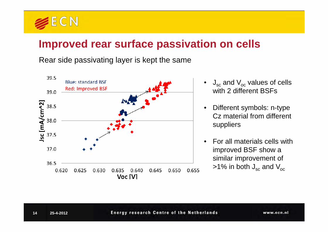
Improved rear surface passivation on cells
• Jsc and Voc values of cells with 2 different BSFs
• Different symbols: n-type Cz material from different
Rear side passivating layer is kept the same
14 25-4-2012
Cz material from different suppliers
• For all materials cells with improved BSF show a similar improvement of >1% in both Jsc and Voc
Cell resultsBalance all requirements:• Good passivation and low absorption: high Voc, Jsc
• Good contact resistance with rear metallization: high FF• Sufficient lateral conduction: high FF
15 25-4-2012
Cell resultsBalance all requirements:• Good passivation and low absorption: high Voc, Jsc
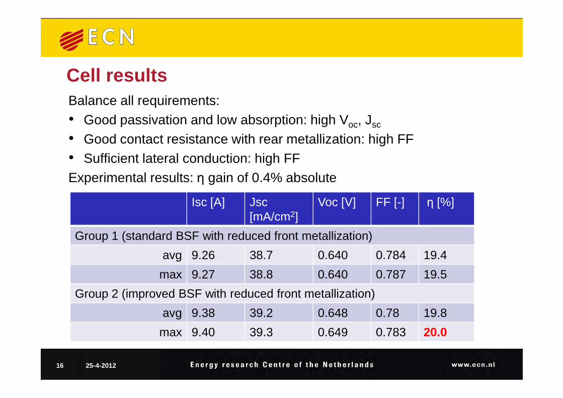
• Good contact resistance with rear metallization: high FF• Sufficient lateral conduction: high FFExperimental results: η gain of 0.4% absolute
Isc [A] Jsc Voc [V] FF [-] η [%]
16 25-4-2012
Isc [A] Jsc[mA/cm2]
Voc [V] FF [-] η [%]
Group 1 (standard BSF with reduced front metallization)
avg 9.26 38.7 0.640 0.784 19.4
max 9.27 38.8 0.640 0.787 19.5
Group 2 (improved BSF with reduced front metallization)
avg 9.38 39.2 0.648 0.78 19.8
max 9.40 39.3 0.649 0.783 20.0
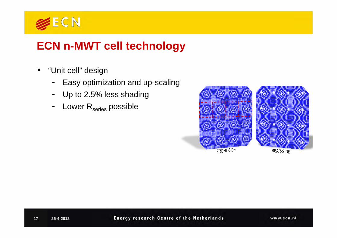
• “Unit cell” design
- Easy optimization and up-scaling
- Up to 2.5% less shading
- Lower Rseries possible
ECN n-MWT cell technology
17 25-4-2012
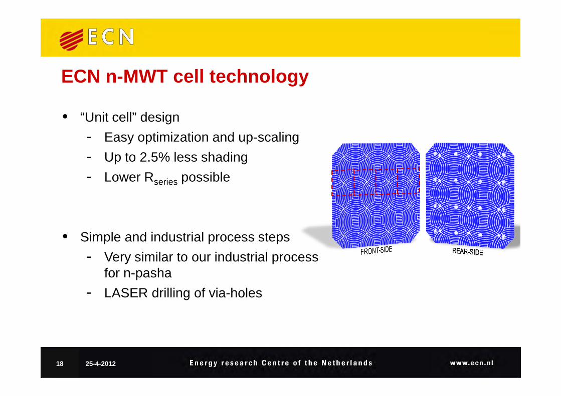
• “Unit cell” design
- Easy optimization and up-scaling
- Up to 2.5% less shading
- Lower Rseries possible
ECN n-MWT cell technology
• Simple and industrial process steps
- Very similar to our industrial processfor n-pasha
- LASER drilling of via-holes
18 25-4-2012
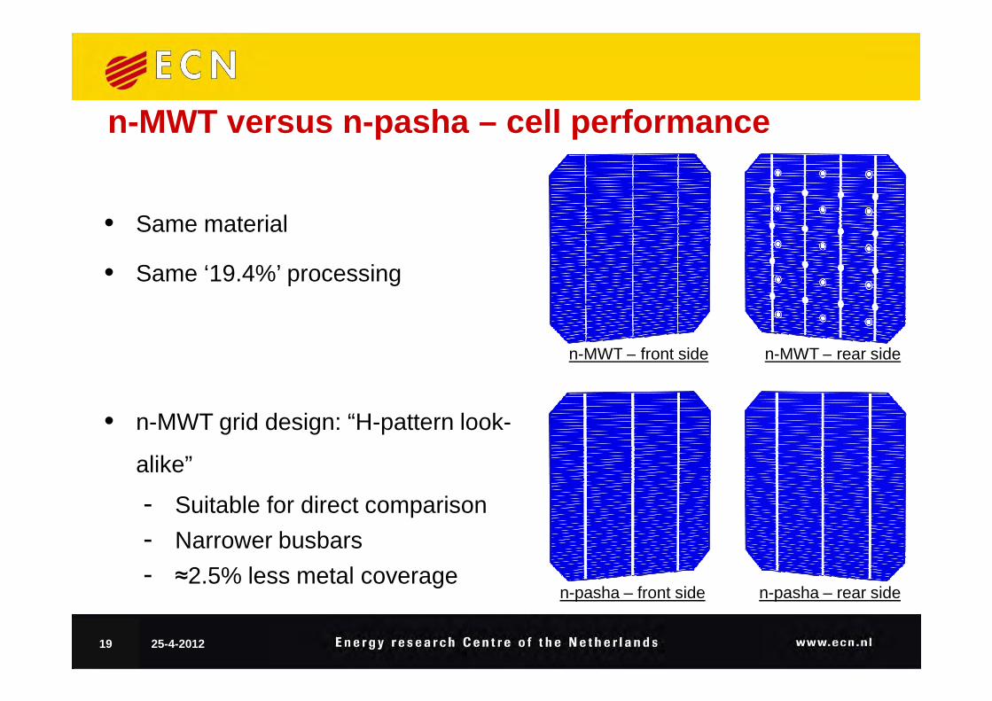
• Same material
• Same ‘19.4%’ processing
n-MWT – front side n-MWT – rear side
n-MWT versus n-pasha – cell performance
• n-MWT grid design: “H-pattern look-
alike”
- Suitable for direct comparison
- Narrower busbars
- ≈2.5% less metal coverage
n-MWT – front side
n-pasha – rear siden-pasha – front side
n-MWT – rear side
19 25-4-2012
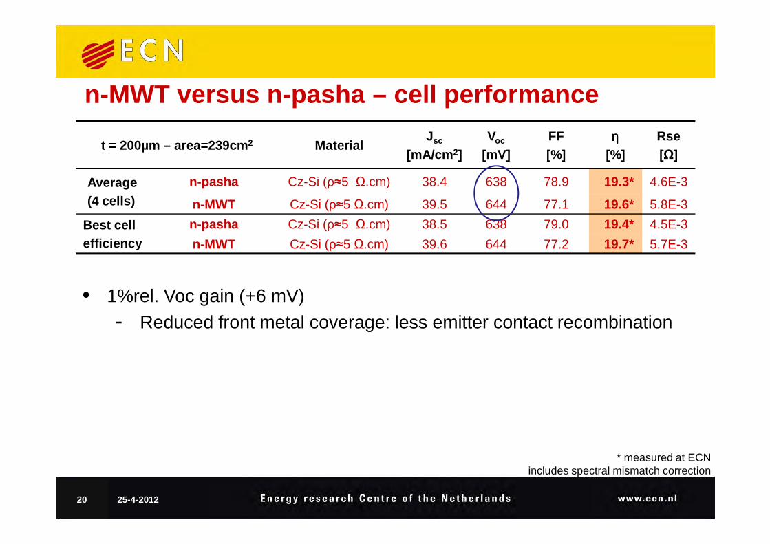
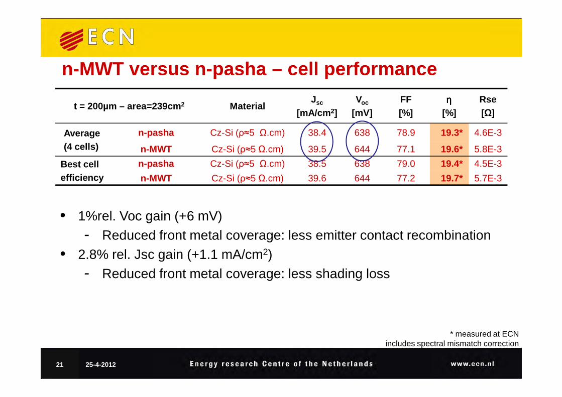
t = 200µm – area=239cm 2 MaterialJsc
[mA/cm 2]Voc
[mV]FF[%]
ηηηη[%]
Rse[Ω]
Average (4 cells)
n-pasha Cz-Si (ρ≈5 Ω.cm) 38.4 638 78.9 19.3* 4.6E-3
n-MWT Cz-Si (ρ≈5 Ω.cm) 39.5 644 77.1 19.6* 5.8E-3
Best cell efficiency
n-pasha Cz-Si (ρ≈5 Ω.cm) 38.5 638 79.0 19.4* 4.5E-3
n-MWT Cz-Si (ρ≈5 Ω.cm) 39.6 644 77.2 19.7* 5.7E-3
n-MWT versus n-pasha – cell performance
* measured at ECN includes spectral mismatch correction
• 1%rel. Voc gain (+6 mV)- Reduced front metal coverage: less emitter contact recombination
20 25-4-2012
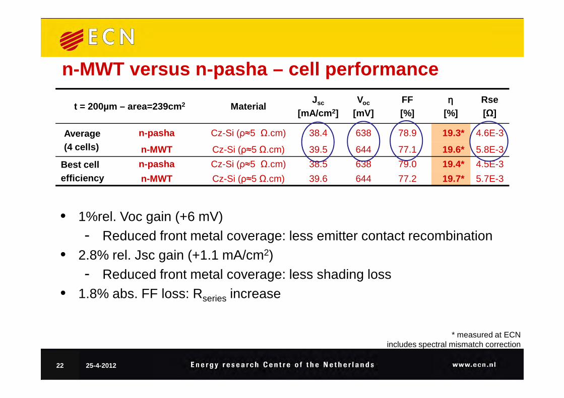
t = 200µm – area=239cm 2 MaterialJsc
[mA/cm 2]Voc
[mV]FF[%]
ηηηη[%]
Rse[Ω]
Average (4 cells)
n-pasha Cz-Si (ρ≈5 Ω.cm) 38.4 638 78.9 19.3* 4.6E-3
n-MWT Cz-Si (ρ≈5 Ω.cm) 39.5 644 77.1 19.6* 5.8E-3
Best cell efficiency
n-pasha Cz-Si (ρ≈5 Ω.cm) 38.5 638 79.0 19.4* 4.5E-3
n-MWT Cz-Si (ρ≈5 Ω.cm) 39.6 644 77.2 19.7* 5.7E-3
n-MWT versus n-pasha – cell performance
* measured at ECN includes spectral mismatch correction
• 1%rel. Voc gain (+6 mV)- Reduced front metal coverage: less emitter contact recombination
• 2.8% rel. Jsc gain (+1.1 mA/cm2)- Reduced front metal coverage: less shading loss
21 25-4-2012
t = 200µm – area=239cm 2 MaterialJsc
[mA/cm 2]Voc
[mV]FF[%]
ηηηη[%]
Rse[Ω]
Average (4 cells)
n-pasha Cz-Si (ρ≈5 Ω.cm) 38.4 638 78.9 19.3* 4.6E-3
n-MWT Cz-Si (ρ≈5 Ω.cm) 39.5 644 77.1 19.6* 5.8E-3
Best cell efficiency
n-pasha Cz-Si (ρ≈5 Ω.cm) 38.5 638 79.0 19.4* 4.5E-3
n-MWT Cz-Si (ρ≈5 Ω.cm) 39.6 644 77.2 19.7* 5.7E-3
n-MWT versus n-pasha – cell performance
* measured at ECN includes spectral mismatch correction
• 1%rel. Voc gain (+6 mV)- Reduced front metal coverage: less emitter contact recombination
• 2.8% rel. Jsc gain (+1.1 mA/cm2)- Reduced front metal coverage: less shading loss
• 1.8% abs. FF loss: Rseries increase
22 25-4-2012
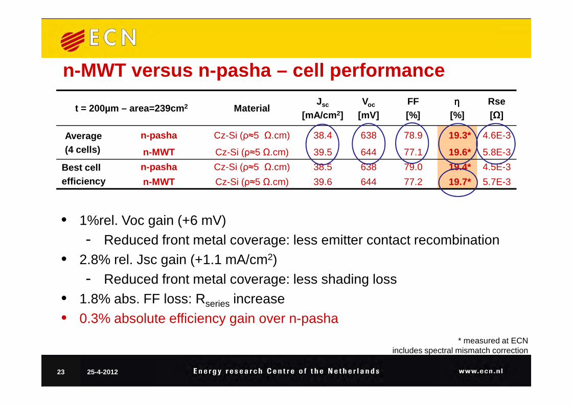
t = 200µm – area=239cm 2 MaterialJsc
[mA/cm 2]Voc
[mV]FF[%]
ηηηη[%]
Rse[Ω]
Average (4 cells)
n-pasha Cz-Si (ρ≈5 Ω.cm) 38.4 638 78.9 19.3* 4.6E-3
n-MWT Cz-Si (ρ≈5 Ω.cm) 39.5 644 77.1 19.6* 5.8E-3
Best cell efficiency
n-pasha Cz-Si (ρ≈5 Ω.cm) 38.5 638 79.0 19.4* 4.5E-3
n-MWT Cz-Si (ρ≈5 Ω.cm) 39.6 644 77.2 19.7* 5.7E-3
n-MWT versus n-pasha – cell performance
* measured at ECN includes spectral mismatch correction
• 1%rel. Voc gain (+6 mV)- Reduced front metal coverage: less emitter contact recombination
• 2.8% rel. Jsc gain (+1.1 mA/cm2)- Reduced front metal coverage: less shading loss
• 1.8% abs. FF loss: Rseries increase• 0.3% absolute efficiency gain over n-pasha
23 25-4-2012
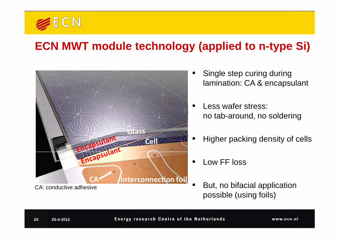
• Single step curing during lamination: CA & encapsulant
• Less wafer stress:no tab-around, no soldering
ECN MWT module technology (applied to n-type Si)
no tab-around, no soldering
• Higher packing density of cells
• Low FF loss
• But, no bifacial application possible (using foils)
Interconnection foilCA
EVA
EVA
Cell
CA: conductive adhesive
24 25-4-2012
Interconnection foilCA
Cell
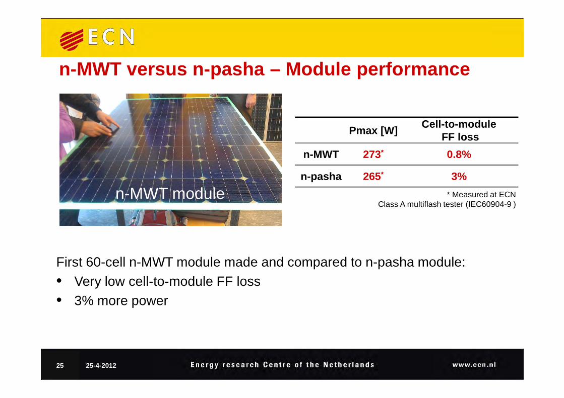
Pmax [W]Cell-to-module
FF loss
n-MWT 273* 0.8%
n-pasha 265* 3%
* Measured at ECN
n-MWT versus n-pasha – Module performance
n-MWT module
First 60-cell n-MWT module made and compared to n-pasha module:• Very low cell-to-module FF loss • 3% more power
Class A multiflash tester (IEC60904-9 ) n-MWT module
25 25-4-2012
Summary and conclusions• Improvements in n-pasha cell process:
- Better process stability- Reduced front metallization (gain 0.3 – 0.4% absolute)- Improved BSF (gain 0.4% absolute)
26 25-4-2012
Summary and conclusions• Improvements in n-pasha cell process:
- Better process stability- Reduced front metallization (gain 0.3 – 0.4% absolute)- Improved BSF (gain 0.4% absolute)
• 20% efficiency obtained•- Using both reduced front metallization and improved BSF- Fully industrial n-pasha process- Ready for industrial implementation
27 25-4-2012
Summary and conclusions• Improvements in n-pasha cell process:
- Better process stability- Reduced front metallization (gain 0.3 – 0.4% absolute)- Improved BSF (gain 0.4% absolute)
• 20% efficiency obtained•- Using both reduced front metallization and improved BSF- Fully industrial n-pasha process- Ready for industrial implementation
• Beyond 20%- Improve emitter and passivation- Further reduce front and rear metallization- 0.3% absolute gain for MWT cell design (19.7% reached so far)
28 25-4-2012
Thank you for your attention !
Bifacial n-pasha cell process with• 20% efficiencyBeyond 20% possible• Improved junctions, passivation
and reduced metallization•
29 25-4-2012
and reduced metallization• MWT
www.npv-workshop.com