Embed Size (px)
DESCRIPTION
電工實驗 ( 四 ) Full Custom Deign Layout Design and Diva Verifications. 老師 : 王進賢 助教 : 李鴻瑜. Outline. Cross Section & Layout View Layout (Design) Rules Layout Edit Diva Verifications (DRC/LVS). gnd. Vin (Poly). Vout. Polysilicon. vdd. thin Oxide. p+. n+. n+. p+. p+. n+. Butting - PowerPoint PPT Presentation
Citation preview
第 1頁
老師 : 王進賢助教 : 李鴻瑜
電工實驗 (四 )
Full Custom DeignLayout Design and Diva Verifications
第 2頁
• Cross Section & Layout View• Layout (Design) Rules• Layout Edit• Diva Verifications (DRC/LVS)
Outline
第 3頁
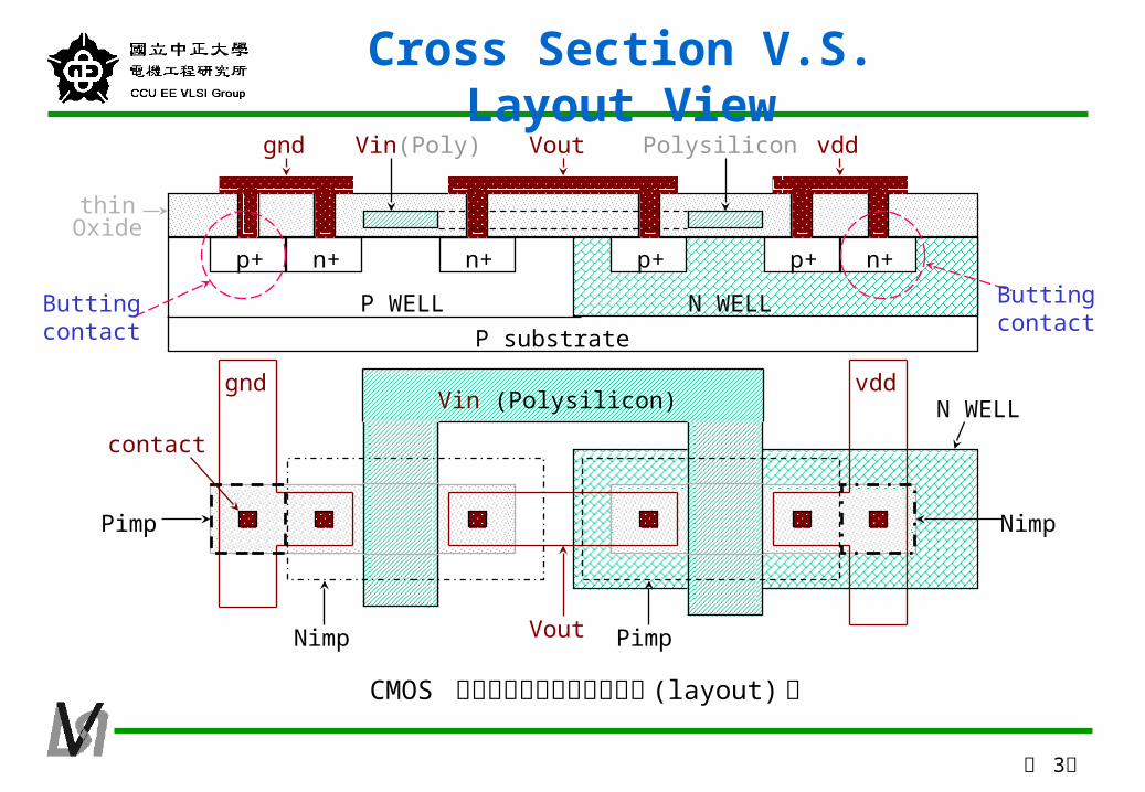
gnd Vout vdd
thinOxide
Vin(Poly) Polysilicon
p+ p+ p+n+ n+ n+
P substrate
N WELL Buttingcontact
Buttingcontact
N WELLVin (Polysilicon)
VoutNimp Pimp
Pimp Nimp
vddgnd
contact
CMOS 的反相器的橫截面圖與佈局 (layout) 圖
P WELL
Cross Section V.S. Layout View
第 4頁
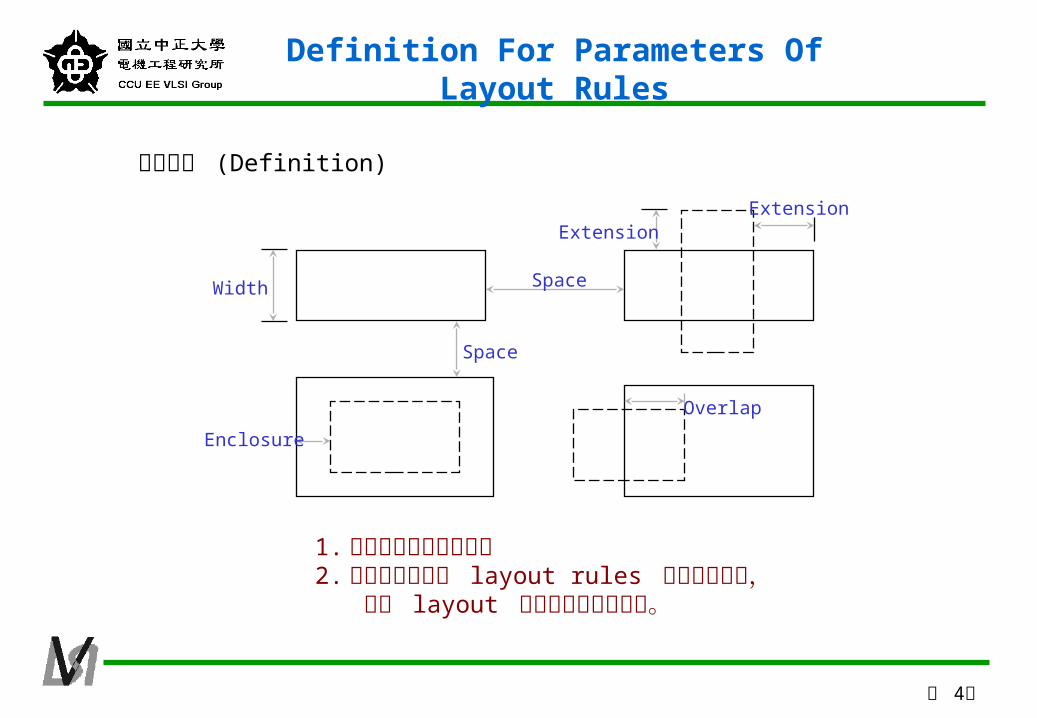
基本定義 (Definition)
Width Space
Space
Enclosure
ExtensionExtension
Overlap
1. 請記住這些名稱的定義2. 接下來所介紹的 layout rules 必須熟記在心, 在劃 layout 時務必遵守這些規則。
Definition For Parameters Of Layout Rules

第 5頁
1. NW (N well)
這二個 NW是同電位的,因為由 Metal 1做為導線連接
這個 NW 的電位與左邊二個 NW的電位是不同的,因為沒有任何的導線做為連接。
n+
n+
Metal 1
NW
NW NW
PW :沒有被 NW 包圍 的區域都視為 P well
1.a1.c
1.b
1.c
1.a
Rule No. Rule Description T-0.6 SPTM 1.a minimum width NW 3.0 1.b minimum space NW-to-NW with different potentials 4.8 1.c minimum space NW-to-NW with the same potentials 1.5
單位為 um
Layout (Design) Rules (I)
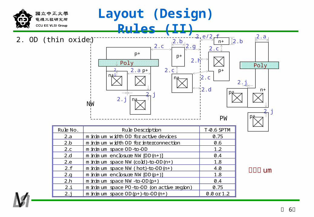
第 6頁
Rule No. Rule Description T-0.6 SPTM 2.a minimum width OD for active devices 0.75 2.b minimum width OD for interconnection 0.6 2.c minimum space OD-to-OD 1.2 2.d minimum enclosure NW[OD(n+)] 0.4 2.e minimum space NW(cold)-to-OD(n+) 1.8 2.f minimum space NW( hot)-to-OD(n+) 4.0 2.g minimum enclosure NW[OD(p+)] 1.8 2.h minimum space NW-to-OD(p+) 0.4 2.i minimum space PO-to-OD (on active region) 0.75 2.j minimum space OD(p+)-to-OD(n+) 0.0 or 1.2
2. OD (thin oxide) 2.e/2.f 2.a
NW
n+
n+
n+
n+
p+
p+p+
p+
p+
p+
n+
Poly Poly
PW
2.a2.i
2.j
2.j
2.j
2.j
2.c2.b
2.g
2.c2.c
2.d
2.h
2.c2.b
單位為 um
Layout (Design) Rules (II)
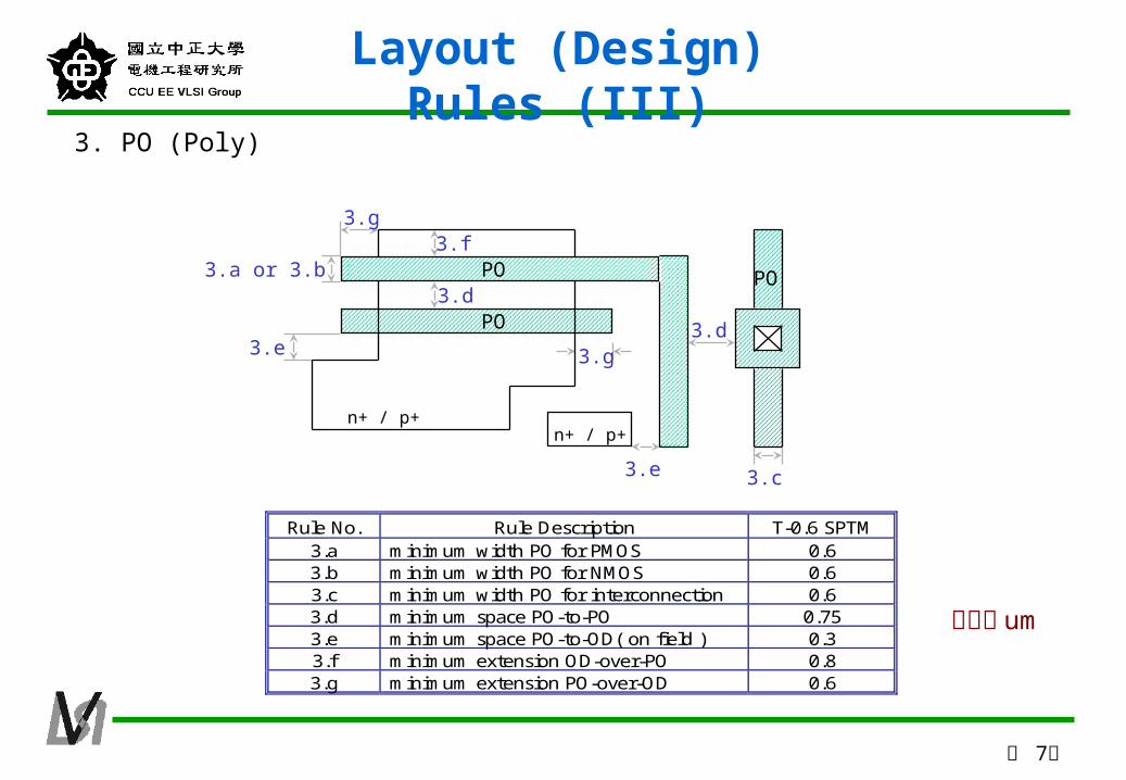
第 7頁
Rule No. Rule Description T-0.6 SPTM3.a minimum width PO for PMOS 0.63.b minimum width PO for NMOS 0.63.c minimum width PO for interconnection 0.63.d minimum space PO-to-PO 0.753.e minimum space PO-to-OD( on field ) 0.33.f minimum extension OD-over-PO 0.83.g minimum extension PO-over-OD 0.6
3. PO (Poly)
n+ / p+
3.g
3.d
3.e
3.a or 3.b
3.e
n+ / p+
PO
PO
PO
3.g3.f
3.d
3.c
單位為 um
Layout (Design) Rules (III)
第 8頁
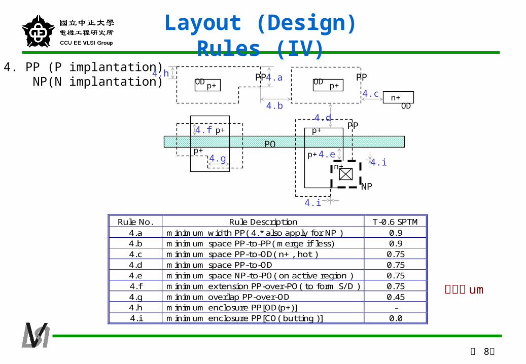
Rule No. Rule Description T-0.6 SPTM 4.a minimum width PP( 4.* also apply for NP ) 0.9 4.b minimum space PP-to-PP( merge if less) 0.9 4.c minimum space PP-to-OD( n+ , hot ) 0.75 4.d minimum space PP-to-OD 0.75 4.e minimum space NP-to-PO( on active region ) 0.75 4.f minimum extension PP-over-PO( to form S/ D ) 0.75 4.g minimum overlap PP-over-OD 0.45 4.h minimum enclosure PP[OD(p+)] - 4.i minimum enclosure PP[CO( butting )] 0.0
4. PP (P implantation) NP(N implantation)
4.c
4.hp+
PO
PP
4.a
4.e
4.b
OD p+OD
n+OD
PPPP
NP
p+
p+ p+
p+
n+ 4.i
4.i
4.d
4.g
4.f
單位為 um
Layout (Design) Rules (IV)
第 9頁
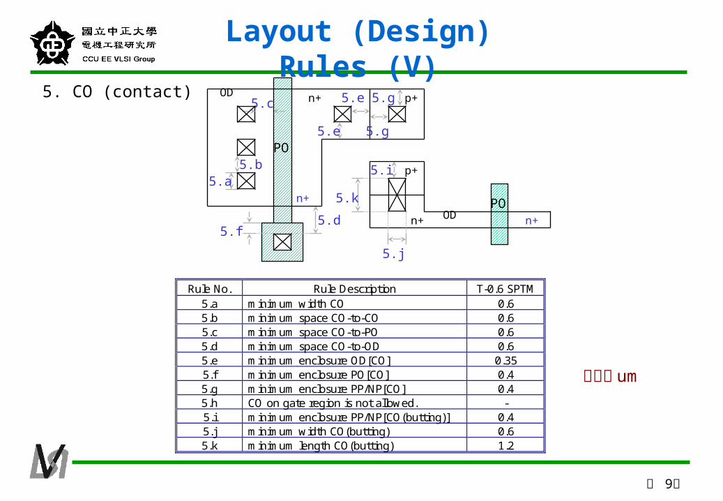
Rule No. Rule Description T-0.6 SPTM5.a minimum width CO 0.65.b minimum space CO-to-CO 0.65.c minimum space CO-to-PO 0.65.d minimum space CO-to-OD 0.65.e minimum enclosure OD[CO] 0.355.f minimum enclosure PO[CO] 0.45.g minimum enclosure PP/NP[CO] 0.45.h CO on gate region is not allowed. -5.i minimum enclosure PP/NP[CO(butting)] 0.45.j minimum width CO(butting) 0.65.k minimum length CO(butting) 1.2
5. CO (contact)
n+
5.c
5.k
5.b
PO
PO
5.a
5.d
5.j
5.fn+
p+5.i
5.g p+
5.g
5.e
5.e
n+
n+
OD
OD
單位為 um
Layout (Design) Rules (V)
第 10頁
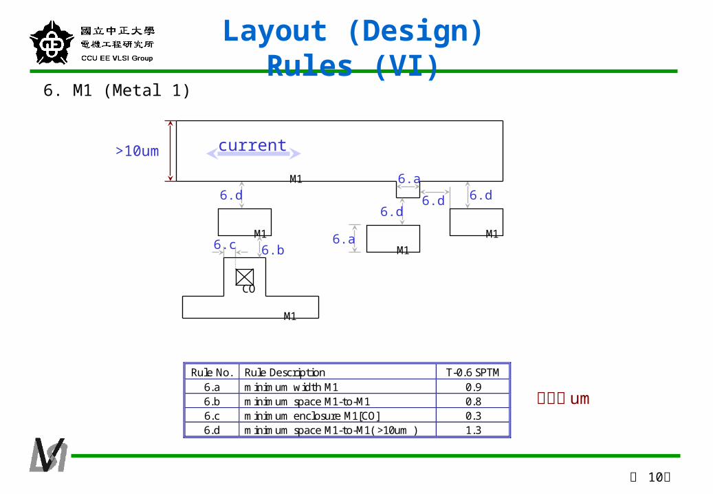
Rule No. Rule Description T-0.6 SPTM 6.a minimum width M1 0.9 6.b minimum space M1-to-M1 0.8 6.c minimum enclosure M1[CO] 0.3 6.d minimum space M1-to-M1( >10um ) 1.3
6. M1 (Metal 1)
6.b
6.d
6.c
CO
M1
6.a
>10um
M1
M1
M1
M1
6.d6.d6.d
6.a
current
單位為 um
Layout (Design) Rules (VI)
第 11頁
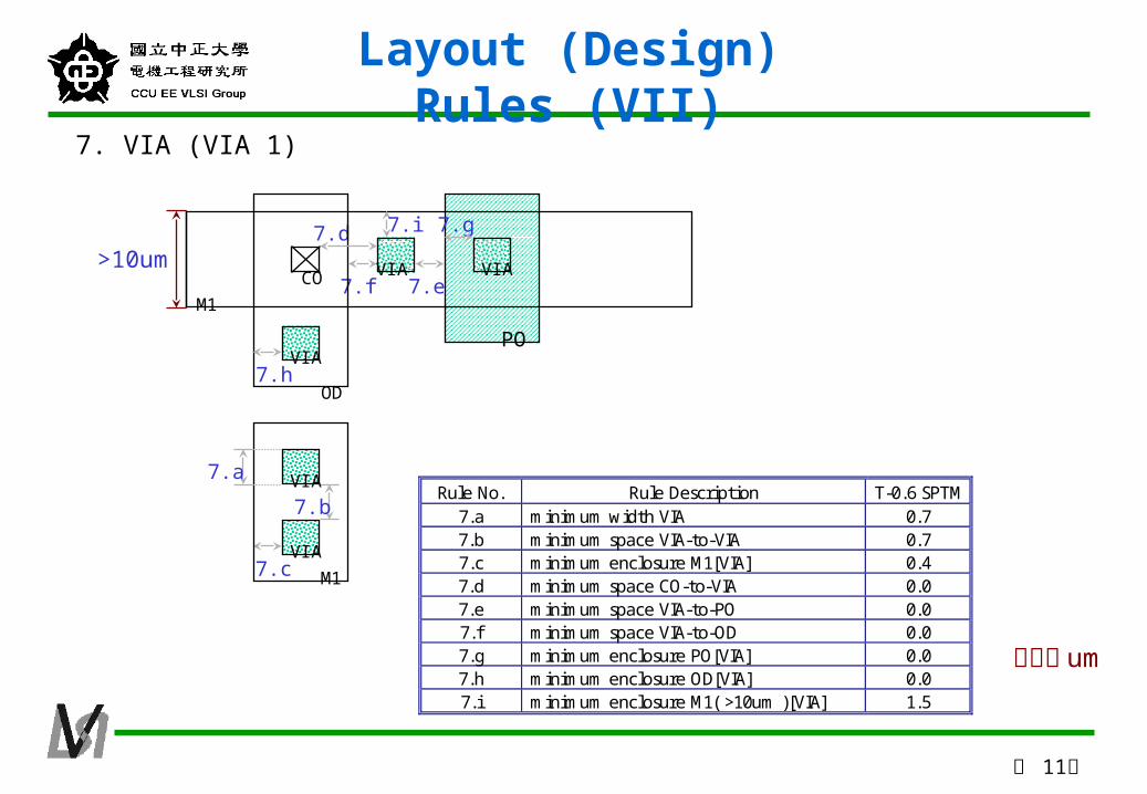
Rule No. Rule Description T-0.6 SPTM 7.a minimum width VIA 0.7 7.b minimum space VIA-to-VIA 0.7 7.c minimum enclosure M1[VIA] 0.4 7.d minimum space CO-to-VIA 0.0 7.e minimum space VIA-to-PO 0.0 7.f minimum space VIA-to-OD 0.0 7.g minimum enclosure PO[VIA] 0.0 7.h minimum enclosure OD[VIA] 0.0 7.i minimum enclosure M1( >10um )[VIA] 1.5
7. VIA (VIA 1)
7.d
7.f
7.a
7.e
OD
PO
7.g
>10um
M1
M1
CO
7.h
7.c
7.bVIA
VIA
VIA
VIAVIA
7.i
單位為 um
Layout (Design) Rules (VII)
第 12頁
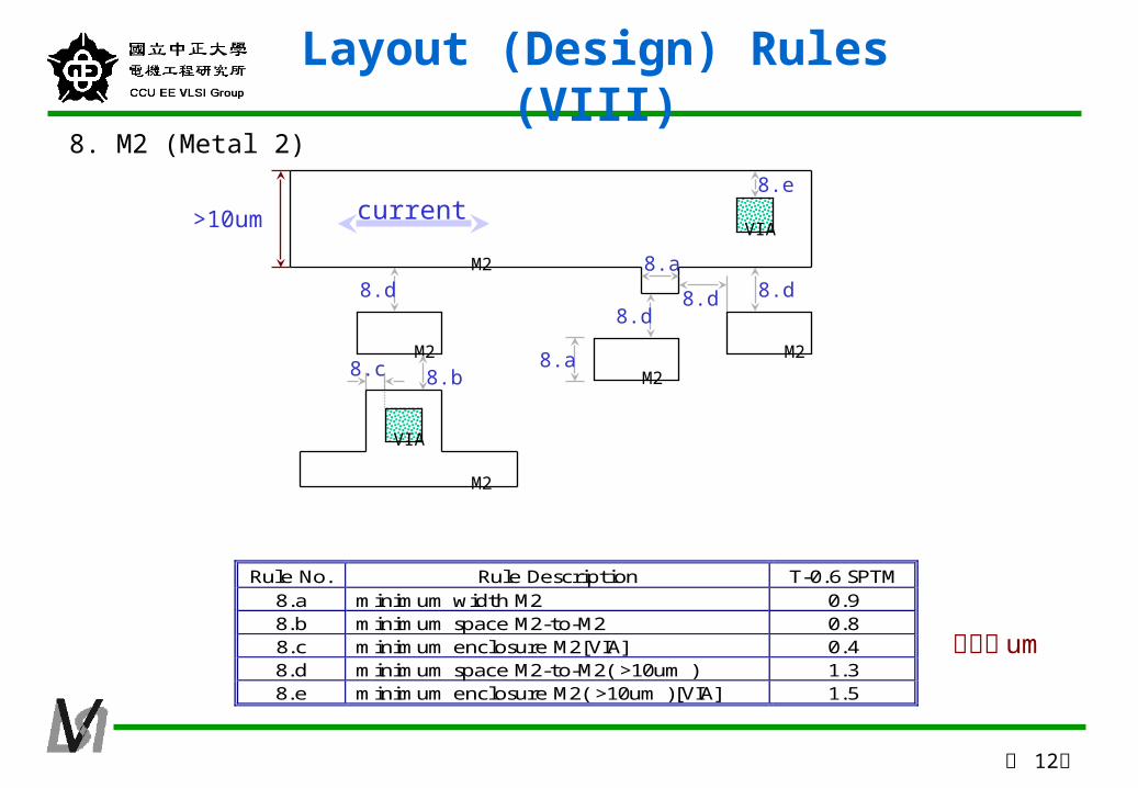
Rule No. Rule Description T-0.6 SPTM 8.a minimum width M2 0.9 8.b minimum space M2-to-M2 0.8 8.c minimum enclosure M2[VIA] 0.4 8.d minimum space M2-to-M2( >10um ) 1.3 8.e minimum enclosure M2( >10um )[VIA] 1.5
8. M2 (Metal 2)
M2
8.b
8.d
8.c
VIA
M2
8.a
>10um
M2
M2
M2
8.d8.d8.d
8.a
currentVIA
8.e
單位為 um
Layout (Design) Rules (VIII)

第 13頁
9. VIA 2
Rule No. Rule Description T-0.6 SPTM 9.a minimum width VIA2 0.7 9.b minimum space VIA2-to-VIA2 0.7 9.c minimum enclosure M2[VIA2] 0.4 9.d minimum enclosure M2( >10um )[VIA2] 1.5 9.e minimum space VIA1-to-VIA2 0.6
9.e 9.a
M1 M3
9.d
>10um
M2
9.a
M29.c
9.b
VIA2
VIA2
VIA1 VIA2
M3
9.b
VIA2
VIA2
9.a
單位為 um
Layout (Design) Rules (IX)
第 14頁
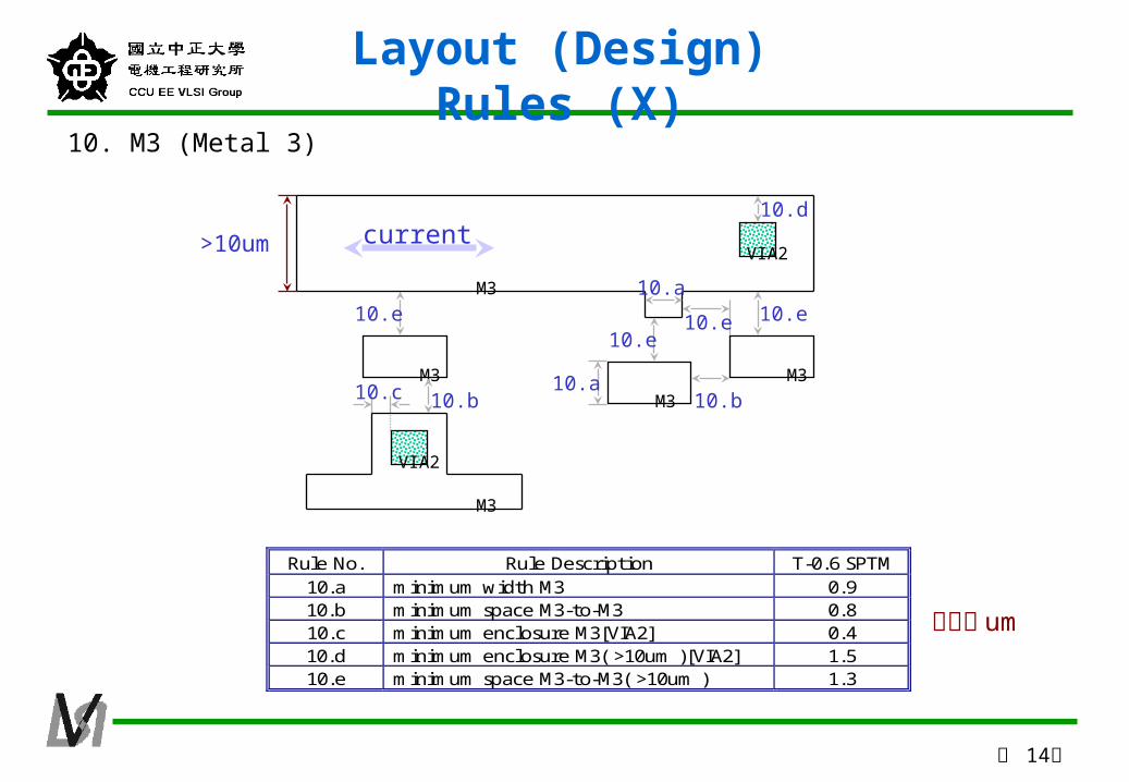
10. M3 (Metal 3)
Rule No. Rule Description T-0.6 SPTM 10.a minimum width M3 0.9 10.b minimum space M3-to-M3 0.8 10.c minimum enclosure M3[VIA2] 0.4 10.d minimum enclosure M3( >10um )[VIA2] 1.5 10.e minimum space M3-to-M3( >10um ) 1.3
M3
10.b
10.e
10.c
VIA2
M3
10.a
>10um
M3
M3
M3
10.e10.e10.e
10.a
current
10.b
VIA2
10.d
單位為 um
Layout (Design) Rules (X)

第 15頁
• Cross Section & Layout View• Layout (Design) Rules• Layout Edit• Diva Verifications (DRC/LVS)
Outline
第 16頁
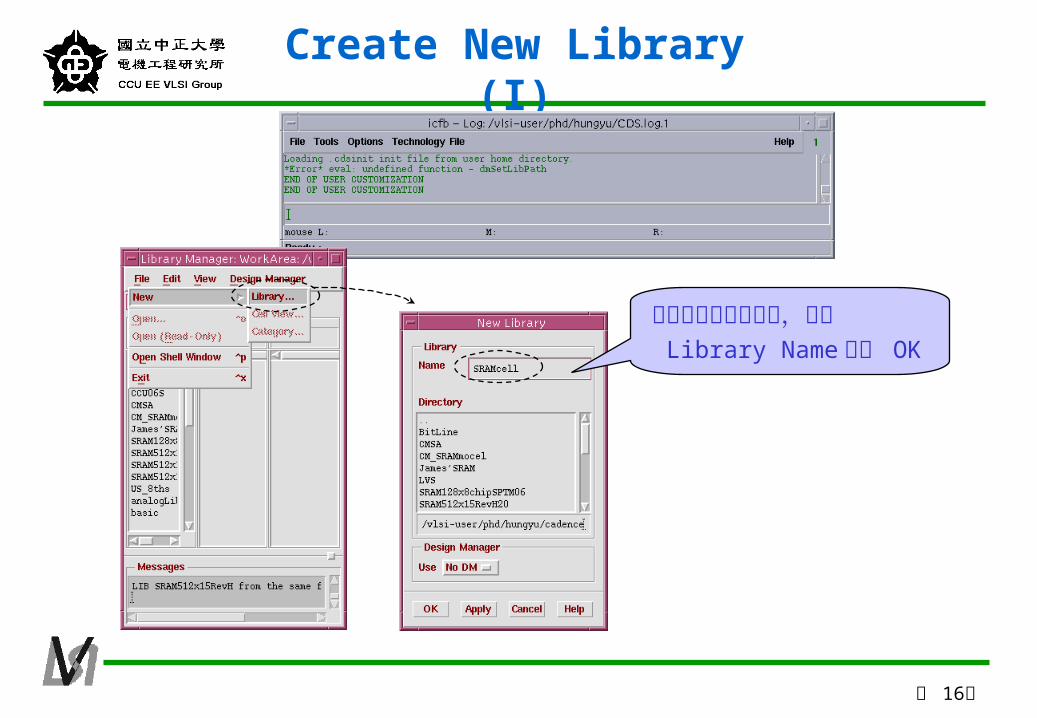
Create New Library (I)
游標指到此處空格內,填入 Library Name 後按 OK
第 17頁
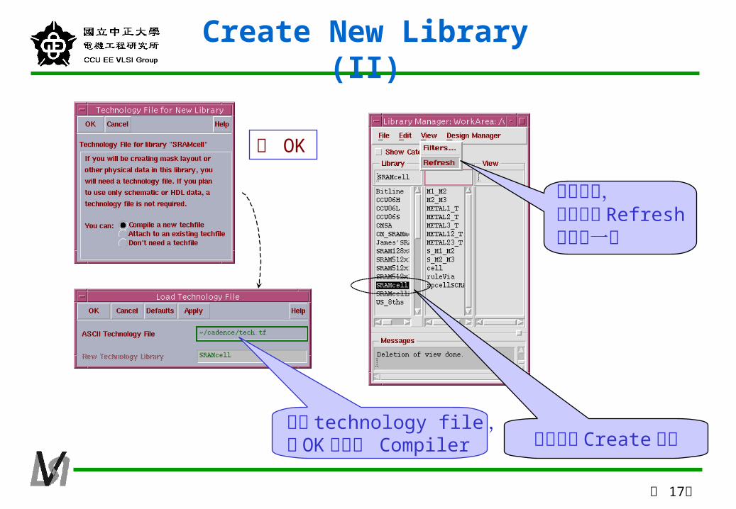
Create New Library (II)
按 OK
填入 technology file ,按 OK 後執行 Compiler 檢查是否 Create 成功
如果沒有,可以重新 Refresh再確認一次
第 18頁
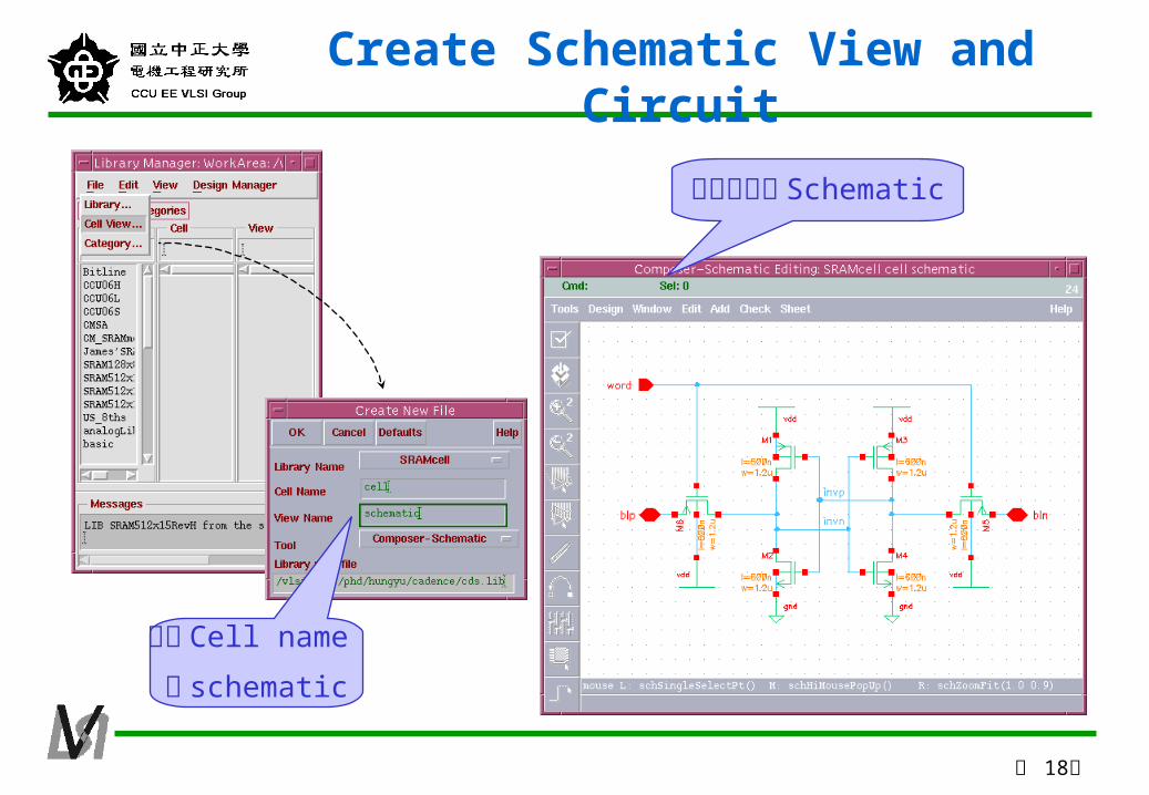
Create Schematic View and Circuit
填入 Cell name
和 schematic
設計並完成 Schematic
第 19頁
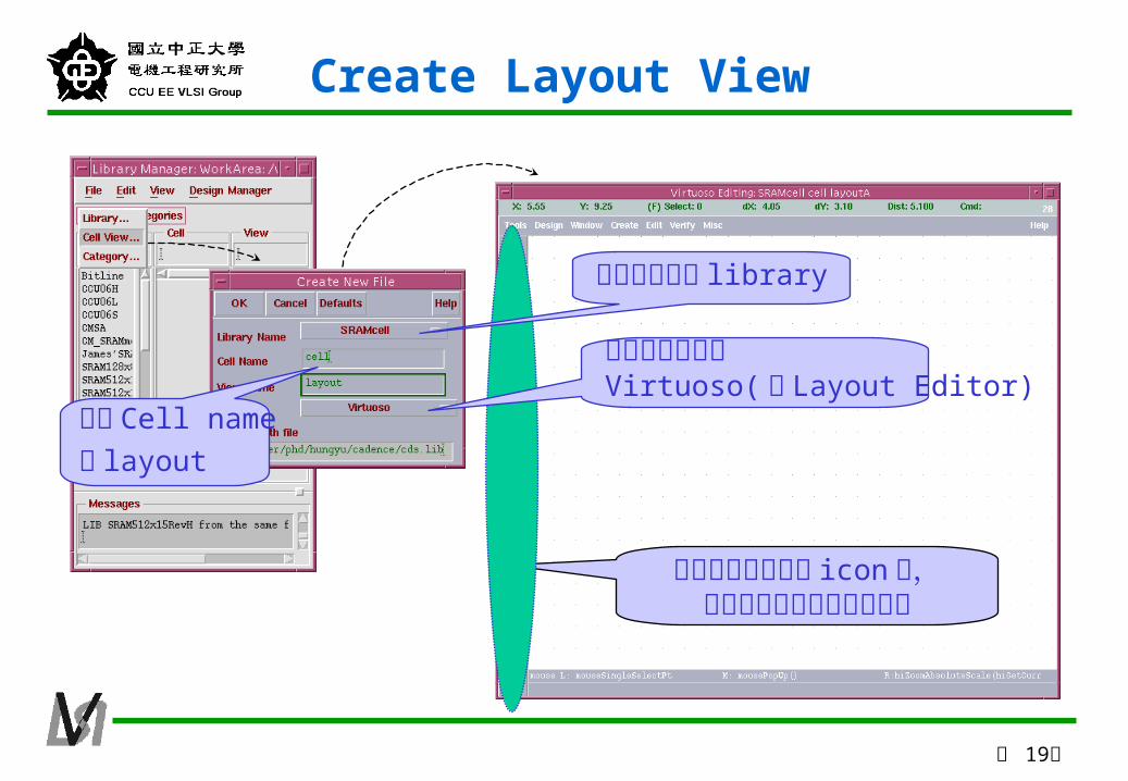
Create Layout View
鍵入 Cell name
和 layout
將滑鼠游標移至各 icon 上,可以看到各種快捷功能說明
選擇欲編輯的 library
應會自動選擇為Virtuoso( 即 Layout Editor)
第 20頁
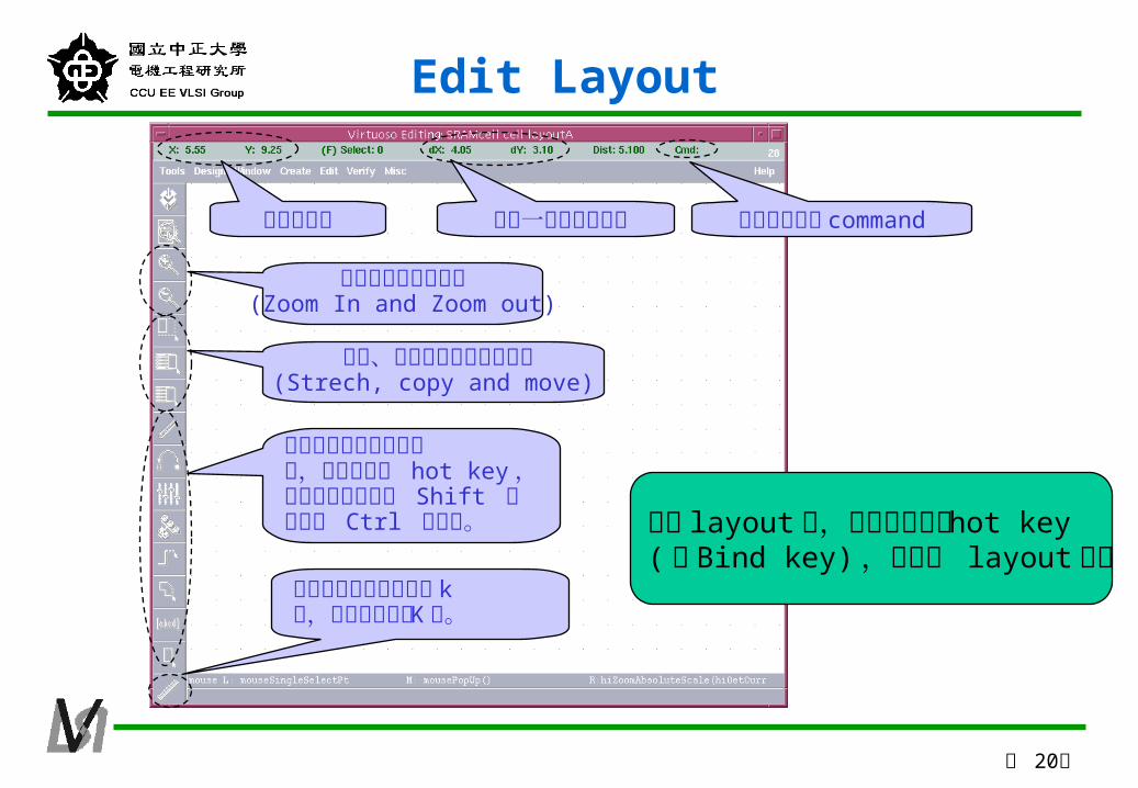
Edit Layout
滑鼠的座標 與上一點的相對位置 目前使用中的 command
放大縮小的快速圖示(Zoom In and Zoom out)
修改、複製及移動的快速圖示(Strech, copy and move)
這些是編輯時的快速圖示,也可以使用 hot key ,在編輯時可以配合 Shift 做加選及 Ctrl 做少選。
量尺寸的快速圖示或按 k鍵,而清除尺寸按 K 鍵。
編輯 layout 時,建議盡量使用 hot key( 即 Bind key) ,以增加 layout 速度
第 21頁
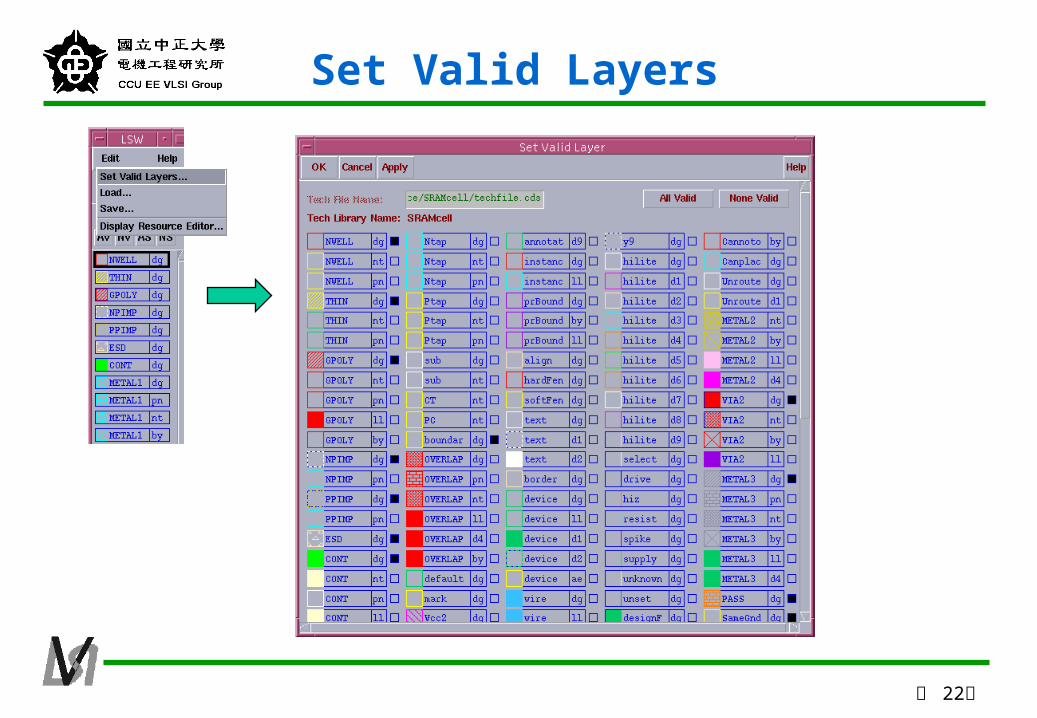
LSW (Layer Select Window)
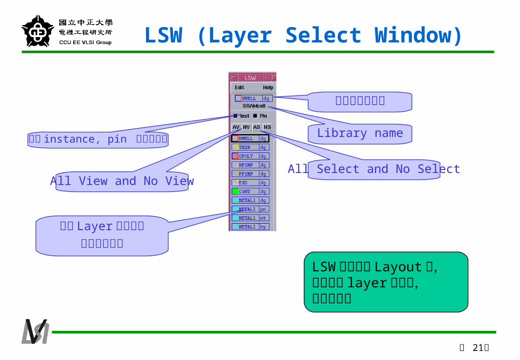
目前所選用的層
Library name設定 instance, pin 是否可編輯
All Select and No SelectAll View and No View
LSW 主要用在 Layout 時,配合各種 layer 的選取,以方便編輯
各種 Layer 可複選成可視或可選擇
第 22頁
Set Valid Layers

第 23頁
Display Resource Editor

第 24頁
NW (N Well)OD (thin oxide)PP (P implantation)NP(N implantation)PO (poly)M1 (metal 1)VIA (VIA 1)CO (contact)M2 (metal 2)
根據 Technology file 內所定義的 Layer name 與
Layout rule 中的 Layer name 之名稱對映。
Layers and display.drf
注意,在 Technology file 內所定義的每一個 Layer name 皆會對映一個 Layer number 。有的 Layer name 會有 dg(drawing) 與 pn(pin) 兩種不同的屬性定義,主要的差別是 purpose 的定義不同,如 dg 是 252 ,而 pn 是 251 。 一般畫 Layout 是使用 dg 的,只有在宣告為 pin 腳時才使用 pn 。
display.drf file

第 25頁
Set Display Options開啟 Display Options 來設定 Grid 。一般Grid 的設法為所有 layout rules 裡的最小單位,在此設為 0.05若是 Grid 沒有設好,則在畫 layout 時將會有很多的困擾,更嚴重可能會有 error 的情形,所以每次開始畫layout 時請務必先做好設定。
設定編輯時游標可以移動的方向
是否顯示 Pin 的Access Edge
第 26頁
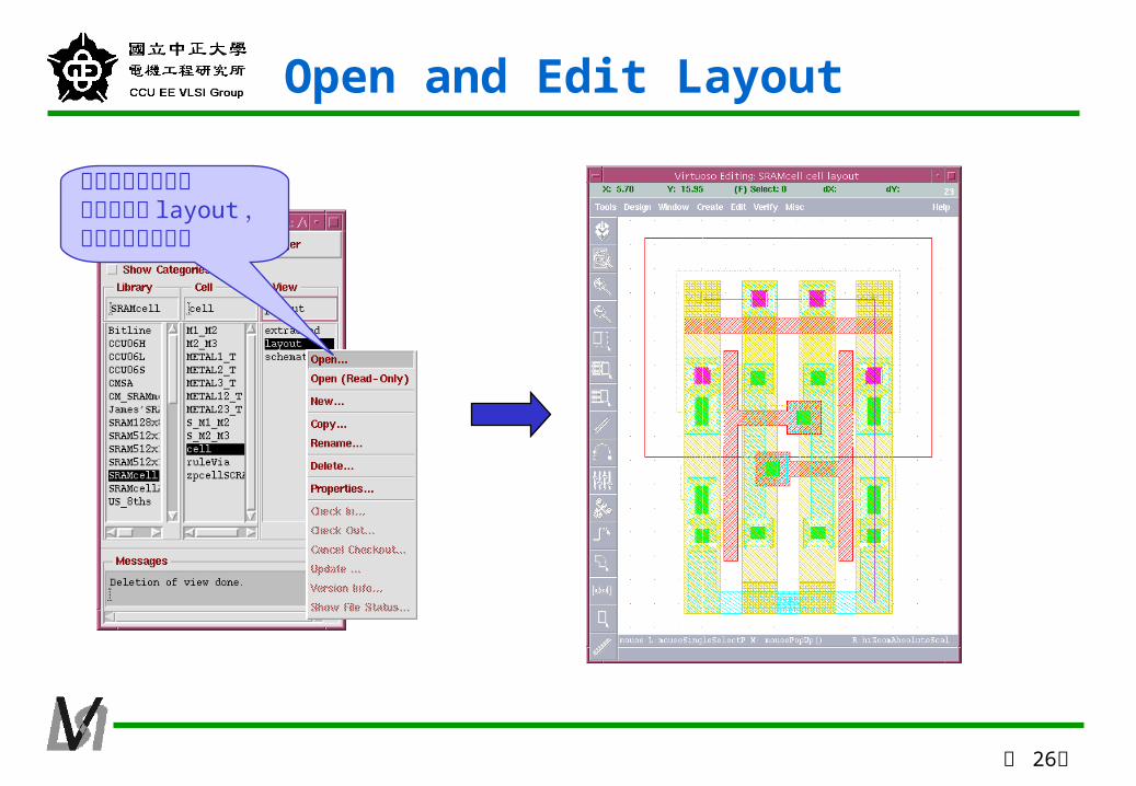
Open and Edit Layout
使用滑鼠中鍵按住點選或雙擊 layout ,可以開出編輯視窗
第 27頁
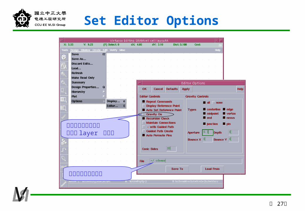
Set Editor Options
取消點選避免游標被吸引到 layer 的邊線
將環境設定到環境檔
第 28頁
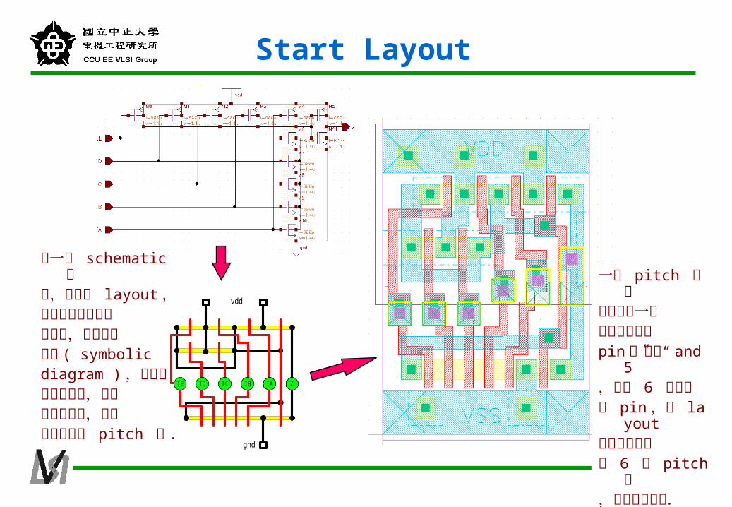
vdd
gnd
ZID IAIBICIE
從一個 schematic 開
始,設計到 layout ,最好事先做好佈局的規劃,如右邊條形圖 ( symbolicdiagram ) ,先簡單粗略的擺設,使其能善用空間,做到使用最少的 pitch 數 .
一個 pitch 最多只能存在一個輸出或輸入的 pin 。此為“ and
5”,共有 6 個輸
出入 pin ,而 lay
out 的結果也只使用 6 個 pitch 數
,所以最省空間 .
Start Layout
第 29頁
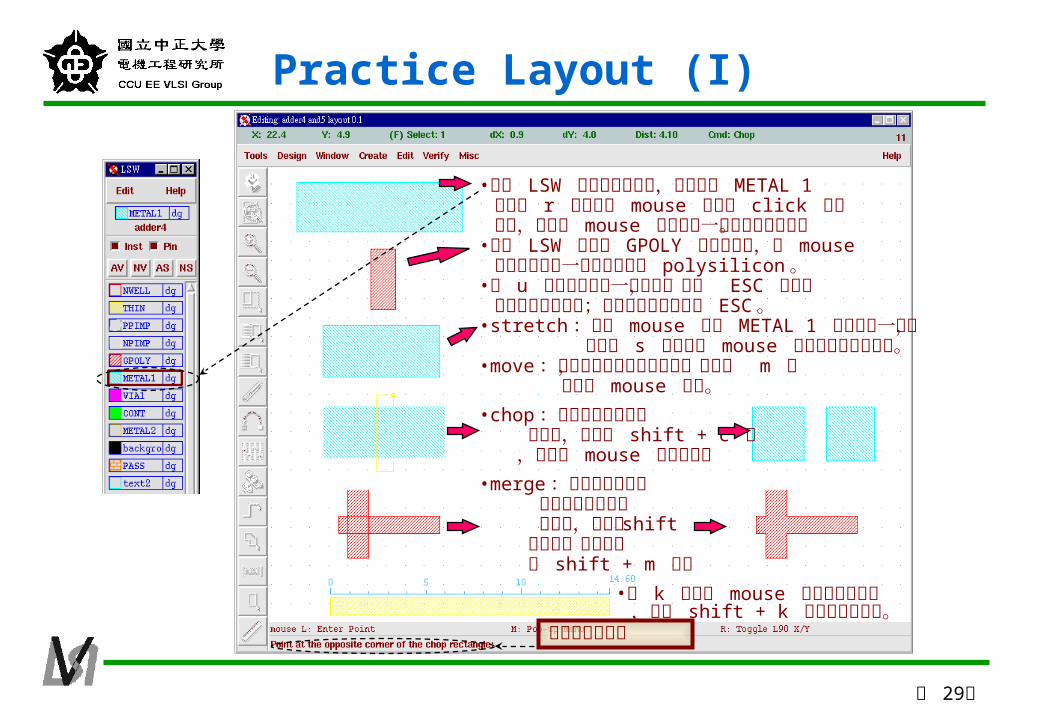
•先至 LSW 內選好要畫的層,在此假設 METAL 1 接著按 r 鍵並配合 mouse 的左鍵 click 做為 起點,而托曳 mouse 即可劃出一個如左圖的矩形。•再到 LSW 內選擇 GPOLY 後同上方式,用 mouse 就可以再畫出一個左圖矩形的 polysilicon 。•按 u 鍵可以取消前一個動作,而按 ESC 鍵則取 消目前的這個命令;每次更換命令最好按 ESC 。•stretch :先用 mouse 輕點 METAL 1 矩形的某一邊,
之後按 s 鍵並配合 mouse 即可改變矩形的大小。
•move :任意選擇所要搬移的目標,之後按 m 鍵 並配合 mouse 即可。•chop :任意選擇所要分割 的矩形,之後按 shift + c 鍵 ,再利用 mouse 來剪開矩形•merge :只限於相同的層 任意框選所要結合 的矩形,或利用 shift 來加選,等確定後 按 shift + m 即可目前命令的說明
•按 k 鍵配合 mouse 可以畫出尺規線 ,而按 shift + k 鍵則清除尺規線。
Practice Layout (I)
第 30頁
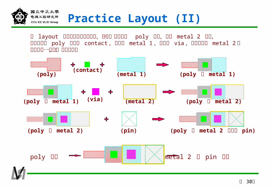
畫 layout 必須有層次的先後關念,例如一個訊號從 poly 輸入,而從 metal 2 輸出,就必須先畫 poly 再疊上 contact ,再疊上 metal 1 ,再疊上 via ,最後再疊上 metal 2 。其過程缺一不可。如下所示:
(poly) (metal 1)(contact)
(poly 到 metal 1)
(poly 到 metal 1) (via) (metal 2) (poly 到 metal 2)
(poly 到 metal 2) (poly 到 metal 2 加輸出 pin)(pin)
poly 輸入 metal 2 的 pin 輸出
Practice Layout (II)
第 31頁
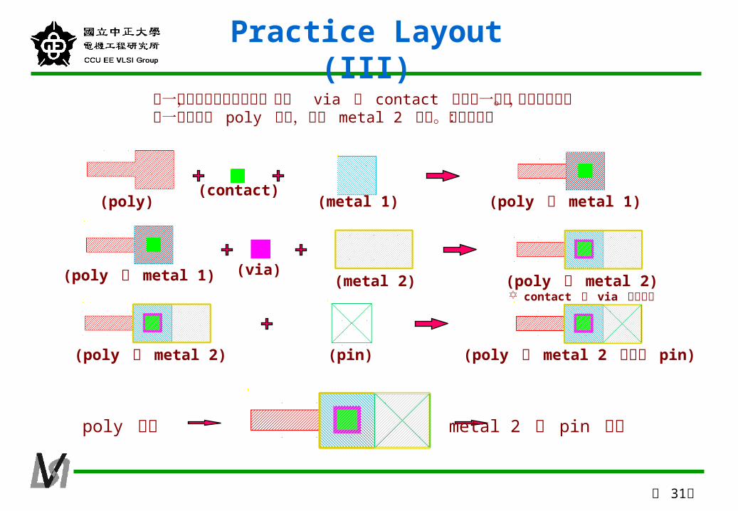
另一種方法比較節省面積,就是 via 與 contact 重疊在一起。同樣的例子,如一個訊號從 poly 輸入,而從 metal 2 輸出。如下所示:
(poly) (metal 1)(contact)
(poly 到 metal 1)
(poly 到 metal 1) (via)(metal 2)
(poly 到 metal 2) (poly 到 metal 2 加輸出 pin)(pin)
poly 輸入 metal 2 的 pin 輸出
(poly 到 metal 2) contact 被 via 完全包住
Practice Layout (III)
第 32頁
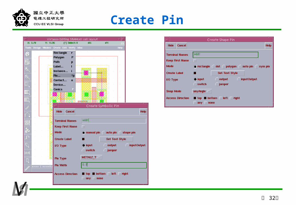
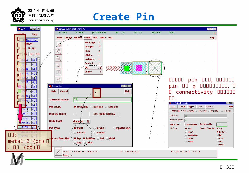
Create Pin
第 33頁
注意:metal 2 (pn) 層,而非 (dg) 層
現在來學習加pin
吧,開始
若要再察看 pin 的屬性,只要用先選好 pin 後按 q 鍵即開出如下的視窗,選擇 connectivity 便可察看甚至修改。
Create Pin
第 34頁
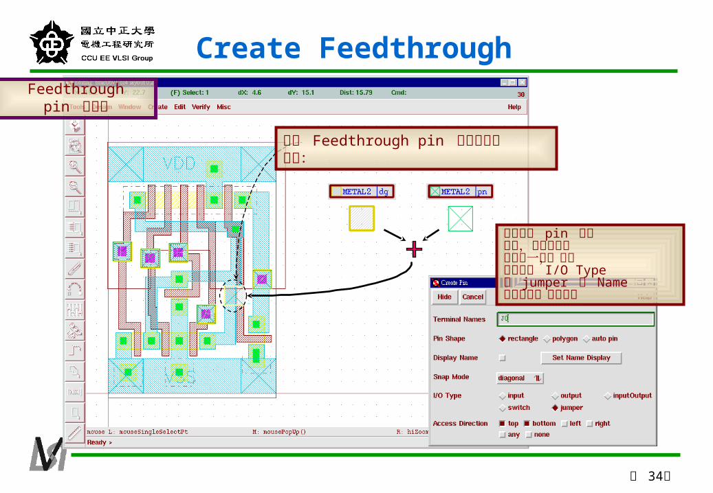
此為 Feedthrough pin 其基本組合如下:
此為設定 pin 時的 參考,建立過程請參考上一頁,值得注意的是 I/O Type選 jumper 而 Name任意取名,但不重複
Feedthroughpin 的建立
Create Feedthrough
第 35頁
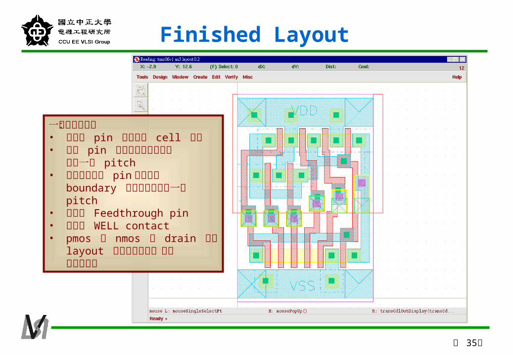
一般注意事項:• 輸出入 pin 盡量拉至 cell 中心• 兩個 pin 的中心點相互間的距離是一個 pitch
• 最外面的二個 pin 中心點與boundary 的距離是二分之一個pitch
• 盡量加 Feedthrough pin• 盡量加 WELL contact• pmos 及 nmos 的 drain 端在
layout 時盡可能靠近,使其面積為最小
Finished Layout
第 36頁
• Cross Section & Layout View• Layout (Design) Rules• Layout Edit• Diva Verifications (DRC/LVS)
Outline
第 37頁
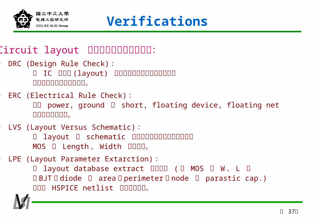
Circuit layout 完成後所須作的驗証如下:• DRC (Design Rule Check) :
對 IC 的佈局 (layout) 作幾何空間的檢查以確保線路能夠被特定的製程技術所實現。
• ERC (Electrical Rule Check) :檢查 power, ground 的 short, floating device, floating net等指定的電氣特性。
• LVS (Layout Versus Schematic) :將 layout 與 schematic 作比對,以檢查電路的連接,與MOS 的 Length 、 Width 值是否配。
• LPE (Layout Parameter Extarction) :從 layout database extract 電氣參數 ( 如 MOS 的 W 、 L 值, BJT , diode 的 area , perimeter , node 的 parastic cap.),並以 HSPICE netlist 方式表示電路。
Verifications
第 38頁
• 光罩或製程在 IC 製過程中是相當昂貴的,所以佈局驗証的重要性自然是不可言喻,一般佈局驗証包括 DRC( Design Rule Check) ,ERC(Electric Rule Check) 及 LVS(Layout vs. Schematic 的比較 ) 。
• Cadence 擁有兩套佈局驗系統: Opus 中的 Diva 是 on-line 交談式,具有快速驗証小 cell 及
與 Opus 完整整合的優點,缺點是對大晶片可能無法作完整驗証,又一般來說, Diva 之 run time 較 Dracula 長。
Dracula 是使用 batch-job 方式, Dracula ( 吸血鬼 ) 被公認是佈局驗証的標準,幾乎全世界所有 IC 公司都拿它來作 sign-off 的憑據。
• 一般 Diva 用於對小 cell 或中型 block 的 layout 設計驗証,而 whole chip 的最後驗証則一定要交由 Dracula 處理。
Diva Versus Dracula
第 39頁
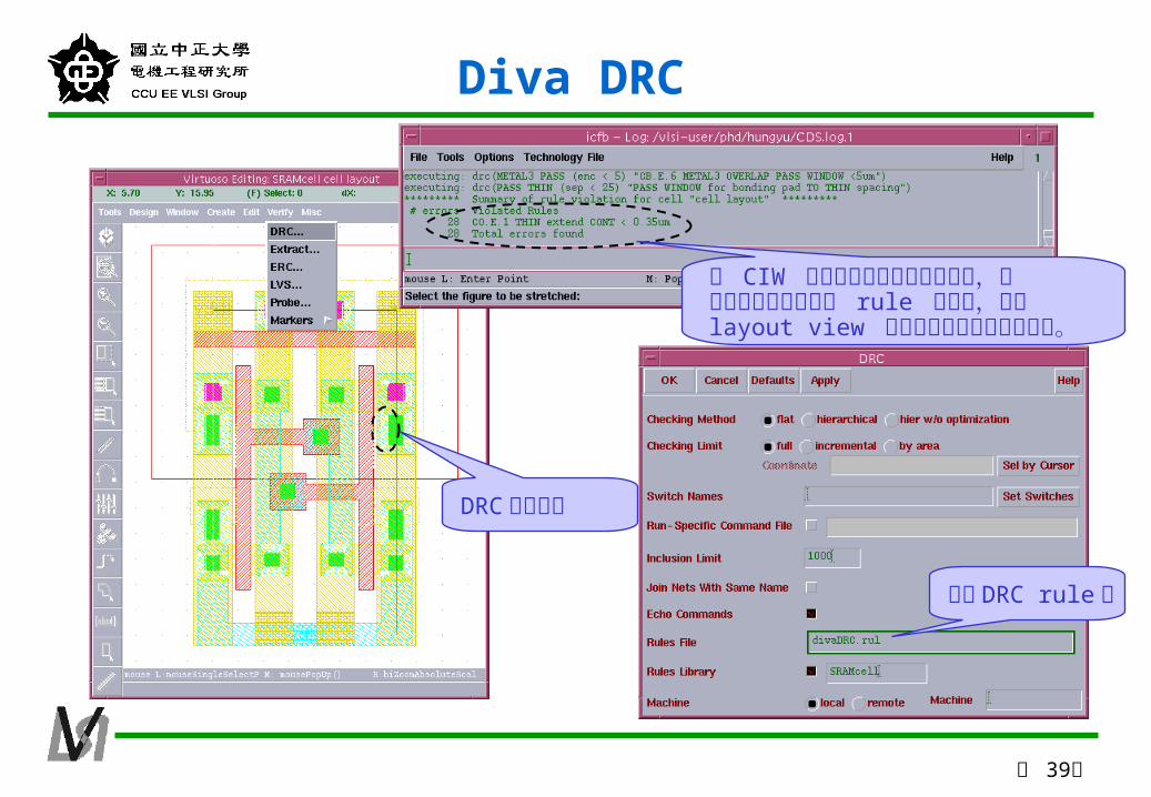
Diva DRC
填入 DRC rule 檔
DRC錯誤顯示
在 CIW 上可以看到檢查過程的訊息,並且在最後會列出違犯 rule 的項目,同時layout view 上亦會以閃動方式顯示錯誤。
第 40頁
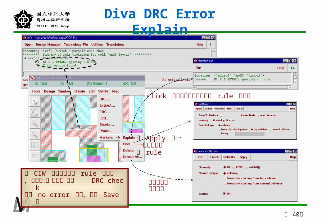
在 CIW 上所看到違犯 rule 的項目
,必須一一解決,直到 DRC check
完全 no error 為止,並做 Save。
click 於閃動處以得悉所違犯 rule 的說明
按 Apply 會一一解釋所違犯的 rule
可以清除閃動的標記
Diva DRC Error Explain
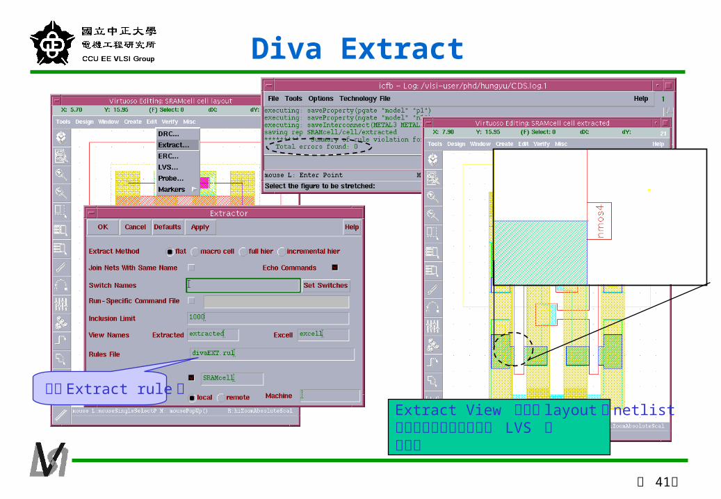
第 41頁
Diva Extract
填入 Extract rule 檔Extract View 會顯示 layout 的 netlist並且抽取出一些參數提供 LVS 時比對。
第 42頁
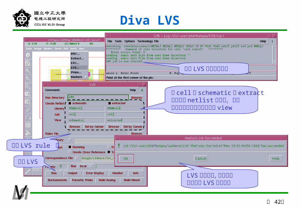
Diva LVS
執行 LVS
顯示 LVS 開始背景執行
LVS 執行結束,但注意此並不表示 LVS比對無誤
將 cell 的 schematic 和 extract 後抽出的 netlist 做比對,可以瀏覽的方式選出所要比對的 view
鍵入 LVS rule 檔
第 43頁
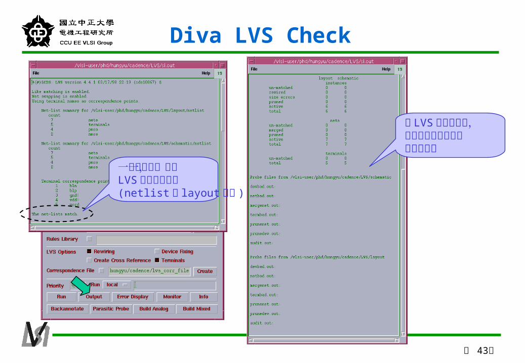
Diva LVS Check
一定要有這一行,LVS比對才算成功(netlist 與 layout 相同 )
若 LVS比對不成功,可以利用以下提供的訊息來偵錯

第 44頁
Probe

第 45頁
按 OK 後,在menu bar 上就增加了一個Abstract 功能
Create Abstract View (I)
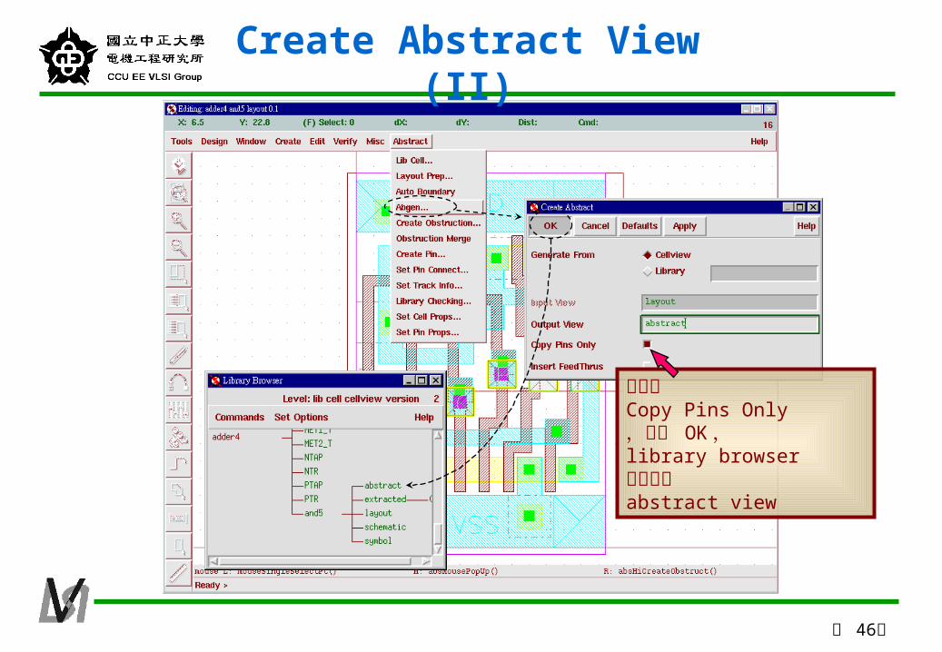
第 46頁
請選擇Copy Pins Only,再按 OK ,library browser就會增加abstract view
Create Abstract View (II)
第 47頁
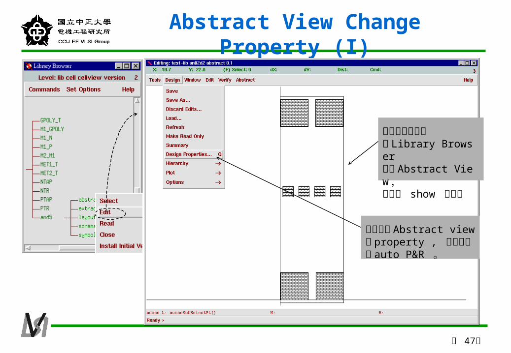
Abstract View Change Property (I)
做完以上的步驟到 Library Browser 開出 Abstract View,且應該 show 如左圖
再設定該 Abstract view 的 property , 使之可以被 auto P&R 。

第 48頁
Abstract View Change Property (II)
按下 Add 鍵
設成 Property
prCellType
standard

第 49頁
Abstract View Change Property (III)
欲去掉不必要的 property information
用 mouse 點此文字部分再按 Delete 即可
設定完後,再 Check & Save