Embed Size (px)
Citation preview

To learn more about ON Semiconductor, please visit our website at www.onsemi.com
Please note: As part of the Fairchild Semiconductor integration, some of the Fairchild orderable part numbers will need to change in order to meet ON Semiconductor’s system requirements. Since the ON Semiconductor product management systems do not have the ability to manage part nomenclature that utilizes an underscore (_), the underscore (_) in the Fairchild part numbers will be changed to a dash (-). This document may contain device numbers with an underscore (_). Please check the ON Semiconductor website to verify the updated device numbers. The most current and up-to-date ordering information can be found at www.onsemi.com. Please email any questions regarding the system integration to [email protected].
Is Now Part of
ON Semiconductor and the ON Semiconductor logo are trademarks of Semiconductor Components Industries, LLC dba ON Semiconductor or its subsidiaries in the United States and/or other countries. ON Semiconductor owns the rights to a number of patents, trademarks, copyrights, trade secrets, and other intellectual property. A listing of ON Semiconductor’s product/patent coverage may be accessed at www.onsemi.com/site/pdf/Patent-Marking.pdf. ON Semiconductor reserves the right to make changes without further notice to any products herein. ON Semiconductor makes no warranty, representation or guarantee regarding the suitability of its products for any particular purpose, nor does ON Semiconductor assume any liability arising out of the application or use of any product or circuit, and specifically disclaims any and all liability, including without limitation special, consequential or incidental damages. Buyer is responsible for its products and applications using ON Semiconductor products, including compliance with all laws, regulations and safety requirements or standards, regardless of any support or applications information provided by ON Semiconductor. “Typical” parameters which may be provided in ON Semiconductor data sheets and/or specifications can and do vary in different applications and actual performance may vary over time. All operating parameters, including “Typicals” must be validated for each customer application by customer’s technical experts. ON Semiconductor does not convey any license under its patent rights nor the rights of others. ON Semiconductor products are not designed, intended, or authorized for use as a critical component in life support systems or any FDA Class 3 medical devices or medical devices with a same or similar classification in a foreign jurisdiction or any devices intended for implantation in the human body. Should Buyer purchase or use ON Semiconductor products for any such unintended or unauthorized application, Buyer shall indemnify and hold ON Semiconductor and its officers, employees, subsidiaries, affiliates, and distributors harmless against all claims, costs, damages, and expenses, and reasonable attorney fees arising out of, directly or indirectly, any claim of personal injury or death associated with such unintended or unauthorized use, even if such claim alleges that ON Semiconductor was negligent regarding the design or manufacture of the part. ON Semiconductor is an Equal Opportunity/Affirmative Action Employer. This literature is subject to all applicable copyright laws and is not for resale in any manner.
FO
D410, F
OD
4108, FO
D4116, F
OD
4118 —
6-Pin
DIP
Hig
h d
v/dt Z
ero-C
ross T
riac Drivers
©2004 Fairchild Semiconductor Corporation www.fairchildsemi.comFOD410, FOD4108, FOD4116, FOD4118 Rev. 1.7.0
October 2016
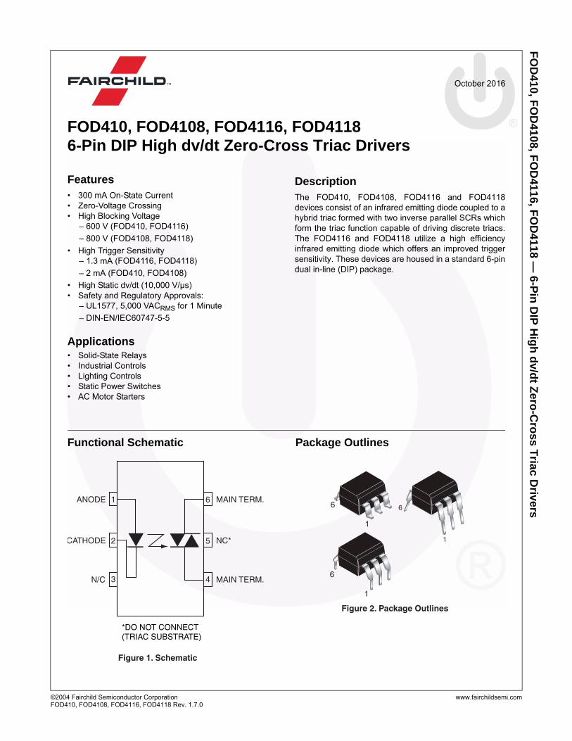
FOD410, FOD4108, FOD4116, FOD4118 6-Pin DIP High dv/dt Zero-Cross Triac Drivers
Features• 300 mA On-State Current• Zero-Voltage Crossing• High Blocking Voltage – 600 V (FOD410, FOD4116)
– 800 V (FOD4108, FOD4118)
• High Trigger Sensitivity – 1.3 mA (FOD4116, FOD4118)
– 2 mA (FOD410, FOD4108)
• High Static dv/dt (10,000 V/μs)• Safety and Regulatory Approvals: – UL1577, 5,000 VACRMS for 1 Minute
– DIN-EN/IEC60747-5-5
Applications• Solid-State Relays • Industrial Controls• Lighting Controls• Static Power Switches• AC Motor Starters
DescriptionThe FOD410, FOD4108, FOD4116 and FOD4118devices consist of an infrared emitting diode coupled to ahybrid triac formed with two inverse parallel SCRs whichform the triac function capable of driving discrete triacs.The FOD4116 and FOD4118 utilize a high efficiencyinfrared emitting diode which offers an improved triggersensitivity. These devices are housed in a standard 6-pindual in-line (DIP) package.
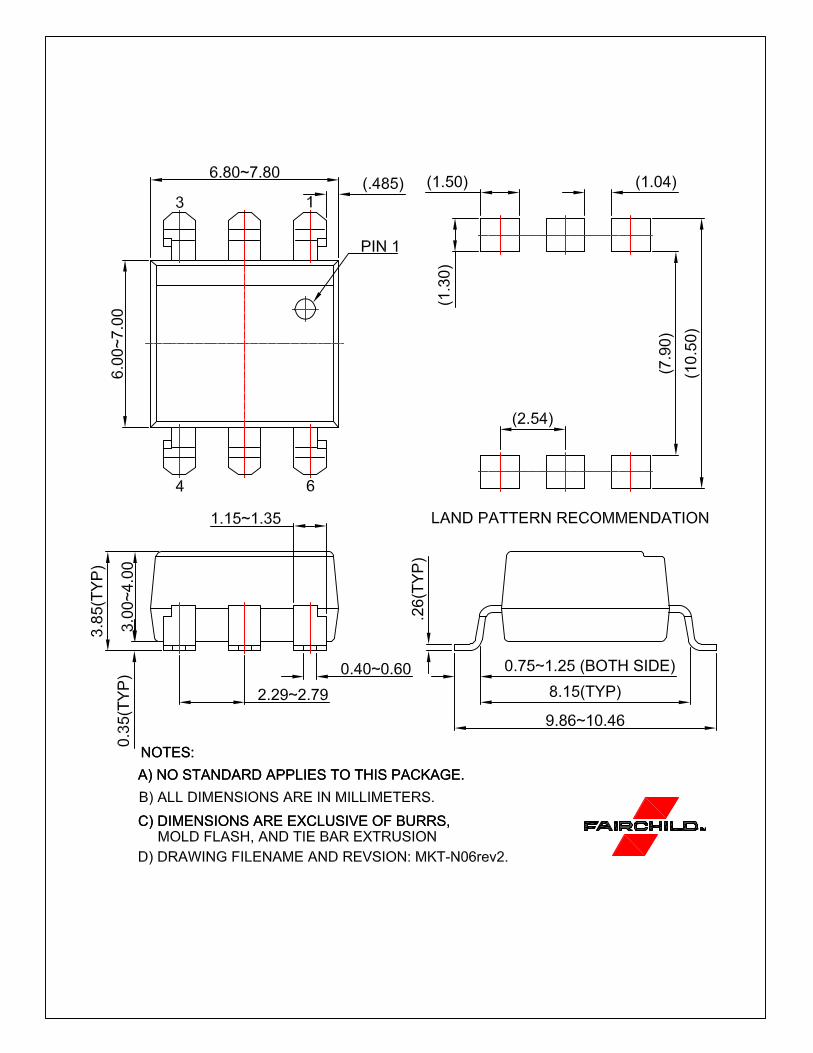
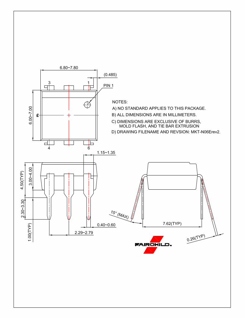
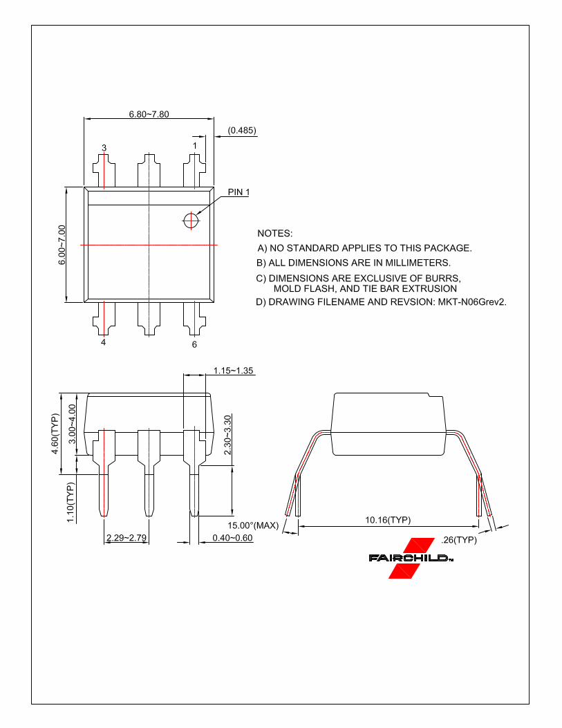
Functional Schematic Package Outlines
6
1
6
6
1
*DO NOT CONNECT(TRIAC SUBSTRATE)
1
Figure 2. Package Outlines
Figure 1. Schematic
MAIN TERM.
NC*
N/C
1
2
3
ANODE
CATHODE
4
5
6 MAIN TERM.
©2004 Fairchild Semiconductor Corporation www.fairchildsemi.comFOD410, FOD4108, FOD4116, FOD4118 Rev. 1.7.0 2
FO
D410, F
OD
4108, FO
D4116, F
OD
4118 —
6-Pin
DIP
Hig
h d
v/dt Z
ero-C
ross T
riac Drivers
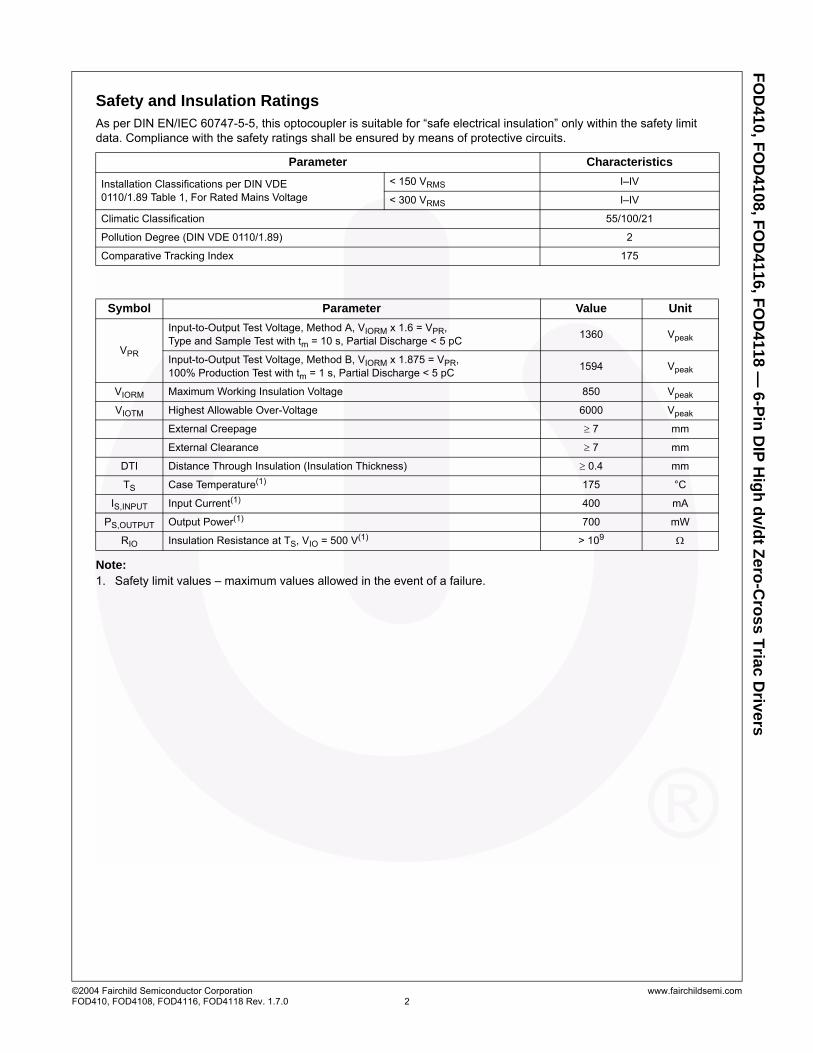
Safety and Insulation RatingsAs per DIN EN/IEC 60747-5-5, this optocoupler is suitable for “safe electrical insulation” only within the safety limit data. Compliance with the safety ratings shall be ensured by means of protective circuits.
Note:1. Safety limit values – maximum values allowed in the event of a failure.
Parameter Characteristics
Installation Classifications per DIN VDE 0110/1.89 Table 1, For Rated Mains Voltage
< 150 VRMS I–IV
< 300 VRMS I–IV
Climatic Classification 55/100/21
Pollution Degree (DIN VDE 0110/1.89) 2
Comparative Tracking Index 175
Symbol Parameter Value Unit
VPR
Input-to-Output Test Voltage, Method A, VIORM x 1.6 = VPR, Type and Sample Test with tm = 10 s, Partial Discharge < 5 pC
1360 Vpeak
Input-to-Output Test Voltage, Method B, VIORM x 1.875 = VPR, 100% Production Test with tm = 1 s, Partial Discharge < 5 pC
1594 Vpeak
VIORM Maximum Working Insulation Voltage 850 Vpeak
VIOTM Highest Allowable Over-Voltage 6000 Vpeak
External Creepage 7 mm
External Clearance 7 mm
DTI Distance Through Insulation (Insulation Thickness) 0.4 mm
TS Case Temperature(1) 175 °C
IS,INPUT Input Current(1) 400 mA
PS,OUTPUT Output Power(1) 700 mW
RIO Insulation Resistance at TS, VIO = 500 V(1) > 109
©2004 Fairchild Semiconductor Corporation www.fairchildsemi.comFOD410, FOD4108, FOD4116, FOD4118 Rev. 1.7.0 3
FO
D410, F
OD
4108, FO
D4116, F
OD
4118 —
6-Pin
DIP
Hig
h d
v/dt Z
ero-C
ross T
riac Drivers
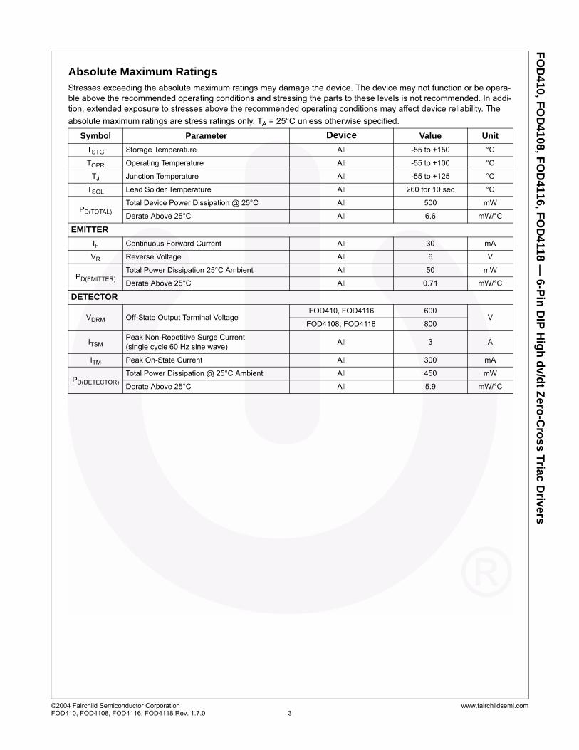
Absolute Maximum Ratings
Stresses exceeding the absolute maximum ratings may damage the device. The device may not function or be opera-ble above the recommended operating conditions and stressing the parts to these levels is not recommended. In addi-tion, extended exposure to stresses above the recommended operating conditions may affect device reliability. The
absolute maximum ratings are stress ratings only. TA = 25°C unless otherwise specified.
Symbol Parameter Device Value Unit
TSTG Storage Temperature All -55 to +150 °C
TOPR Operating Temperature All -55 to +100 °C
TJ Junction Temperature All -55 to +125 °C
TSOL Lead Solder Temperature All 260 for 10 sec °C
PD(TOTAL)
Total Device Power Dissipation @ 25°C All 500 mW
Derate Above 25°C All 6.6 mW/°C
EMITTER
IF Continuous Forward Current All 30 mA
VR Reverse Voltage All 6 V
PD(EMITTER)
Total Power Dissipation 25°C Ambient All 50 mW
Derate Above 25°C All 0.71 mW/°C
DETECTOR
VDRM Off-State Output Terminal VoltageFOD410, FOD4116 600
VFOD4108, FOD4118 800
ITSMPeak Non-Repetitive Surge Current (single cycle 60 Hz sine wave)
All 3 A
ITM Peak On-State Current All 300 mA
PD(DETECTOR)
Total Power Dissipation @ 25°C Ambient All 450 mW
Derate Above 25°C All 5.9 mW/°C
©2004 Fairchild Semiconductor Corporation www.fairchildsemi.comFOD410, FOD4108, FOD4116, FOD4118 Rev. 1.7.0 4
FO
D410, F
OD
4108, FO
D4116, F
OD
4118 —
6-Pin
DIP
Hig
h d
v/dt Z
ero-C
ross T
riac Drivers
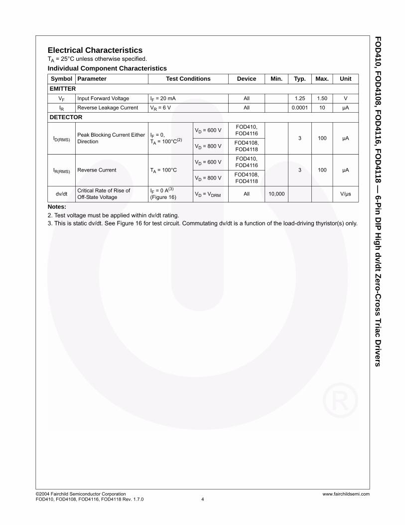
Electrical Characteristics TA = 25°C unless otherwise specified.
Individual Component Characteristics
Notes:
2. Test voltage must be applied within dv/dt rating.3. This is static dv/dt. See Figure 16 for test circuit. Commutating dv/dt is a function of the load-driving thyristor(s) only.
Symbol Parameter Test Conditions Device Min. Typ. Max. Unit
EMITTER
VF Input Forward Voltage IF = 20 mA All 1.25 1.50 V
IR Reverse Leakage Current VR = 6 V All 0.0001 10 μA
DETECTOR
ID(RMS)Peak Blocking Current Either Direction
IF = 0,TA = 100°C(2)
VD = 600 VFOD410,FOD4116
3 100 μA
VD = 800 VFOD4108,FOD4118
IR(RMS) Reverse Current TA = 100°C
VD = 600 VFOD410,FOD4116
3 100 μA
VD = 800 VFOD4108,FOD4118
dv/dtCritical Rate of Rise of Off-State Voltage
IF = 0 A(3) (Figure 16)
VD = VDRM All 10,000 V/μs
©2004 Fairchild Semiconductor Corporation www.fairchildsemi.comFOD410, FOD4108, FOD4116, FOD4118 Rev. 1.7.0 5
FO
D410, F
OD
4108, FO
D4116, F
OD
4118 —
6-Pin
DIP
Hig
h d
v/dt Z
ero-C
ross T
riac Drivers
Electrical Characteristics (Continued)TA = 25°C unless otherwise specified.
Transfer Characteristics
Note:
4. All devices are guaranteed to trigger at an IF value less than or equal to max IFT.Therefore, recommended operating
IF lies between max IFT (2 mA for FOD410 and FOD4108 and 1.3 mA for FOD4116 and FOD4118) and the absolute
max IF (30 mA).
Zero Crossing Characteristics
Isolation Characteristics
Note:
5. Isolation voltage, VISO, is an internal device dielectric breakdown rating. For this test, pins 1, 2 and 3 are common,
and pins 4, 5 and 6 are common. 5,000 VACRMS for 1 minute duration is equivalent to 6,000 VACRMS for 1 second
duration.
Symbol Parameter Test Conditions Device Min. Typ. Max. Unit
IFT LED Trigger Current Main Terminal Voltage = 5 V(4)
FOD410,FOD4108
0.65 2.0
mA FOD4116,FOD4118
0.65 1.3
VTM Peak On-State Voltage, Either Direction
ITM = 300 mA peak, IF = Rated IFT All 2.2 3 V
IH Holding Current, Either Direction
VT = 3 V All 200 500 µA
IL Latching Current VT = 2.2 V All 5 mA
tON Turn-On Time
PF = 1.0, IT = 300 mA
VRM = VDM = 424 VACFOD410, FOD4116, FOD4118 60 µs
VRM = VDM = 565 VAC FOD4108
tOFF Turn-Off TimeVRM = VDM = 424 VAC
FOD410, FOD4116, FOD4118 52 µs
VRM = VDM = 565 VAC FOD4108
dv/dtC
Critical Rate of Rise of Voltage at Current Com-mutation
VD = 230 VRMS,ID = 300 mAPK
All 10 V/µs
di/dtC
Critical Rate of Rise of On-State Current Com-mutation
VD = 230 VRMS,ID = 300 mAPK
All 9 A/ms
dv(IO)/dtCritical Rate ofRise of CoupledInput/Output Voltage
IT = 0 A, VRM = VDM = 424 VAC All 10,000 V/µs
Symbol Parameter Test Conditions Device Min. Typ. Max. Unit
VINH
Inhibit Voltage
(MT1-MT2 Voltage
above which device
will not trigger)
IF = Rated IFT All 8 25 V
IDRM2 Leakage in Inhibit State IF = Rated IFT, Rated VDRM, Off-State All 20 200 µA
Symbol Parameter Test Conditions Device Min. Typ. Max. Unit
VISO Steady State Isolation
Voltagef = 60 Hz, t = 1 Minute(5) All 5,000 VACRMS
©2004 Fairchild Semiconductor Corporation www.fairchildsemi.comFOD410, FOD4108, FOD4116, FOD4118 Rev. 1.7.0 6
FO
D410, F
OD
4108, FO
D4116, F
OD
4118 —
6-Pin
DIP
Hig
h d
v/dt Z
ero-C
ross T
riac Drivers
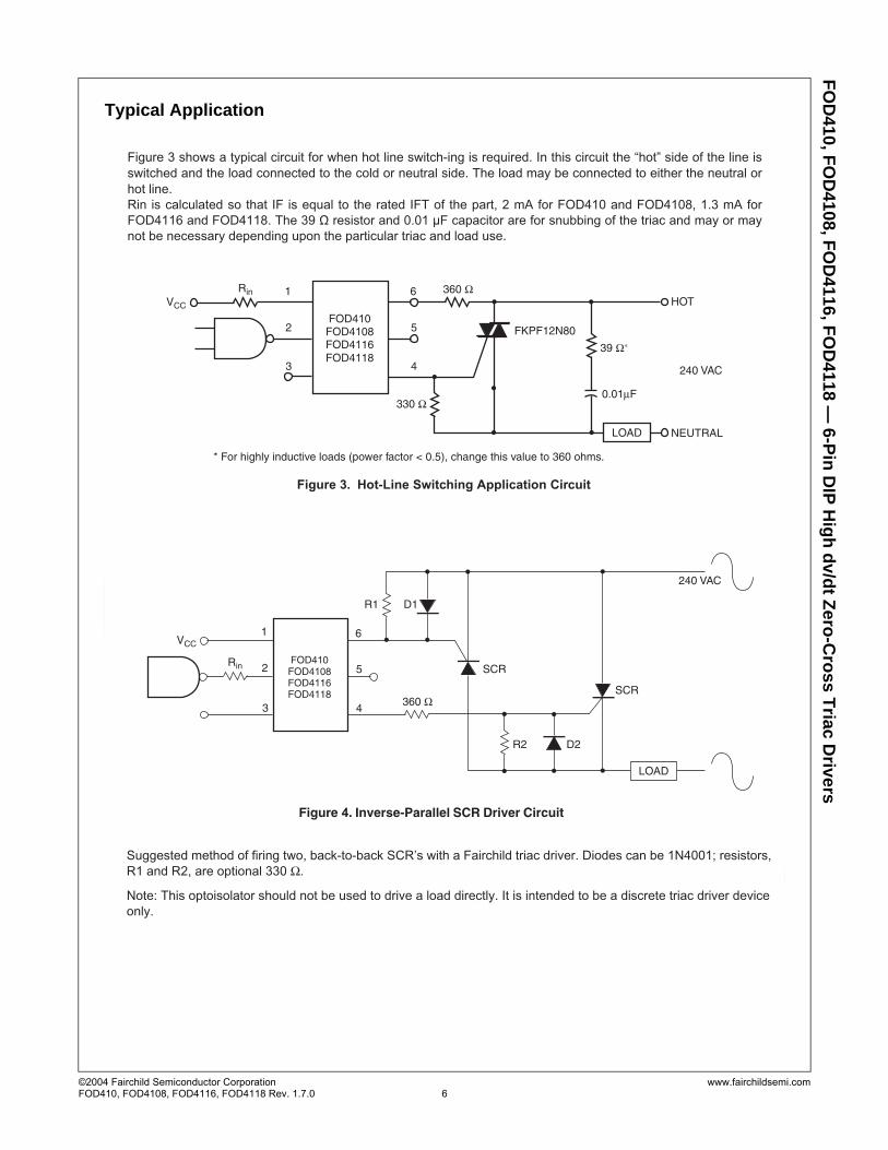
Typical Application
Figure 3 shows a typical circuit for when hot line switch-ing is required. In this circuit the “hot” side of the line is switched and the load connected to the cold or neutral side. The load may be connected to either the neutral or
Figure 3. Hot-Line Switching Application Circuit
0.01μF
VCC
Rin 1
2
3
6
5
4 240 VAC
HOT
FKPF12N80
NEUTRAL
360 Ω
* For highly inductive loads (power factor < 0.5), change this value to 360 ohms.
330 Ω
FOD4 0FOD4 08FOD4 16FOD4 18
39 Ω
LOAD
Figure . Inverse-Parallel SCR Driver Circuit
VCC
Rin
1
2
3
6
5
4
240 VAC
SCR360 Ω
R1 D1
SCR
R2 D2
LOAD
FOD4 0FOD4 08FOD4 16FOD4 18
Suggested method of firing two, back-to-back SCR’s with a Fairchild triac driver. Diodes can be 1N4001; resistors, R1 and R2, are optional 330 Ω.
Note: This optoisolator should not be used to drive a load directly. It is intended to be a discrete triac driver device only.
©2004 Fairchild Semiconductor Corporation www.fairchildsemi.comFOD410, FOD4108, FOD4116, FOD4118 Rev. 1.7.0 7
FO
D410, F
OD
4108, FO
D4116, F
OD
4118 —
6-Pin
DIP
Hig
h d
v/dt Z
ero-C
ross T
riac Drivers
Typical Performance Characteristics
-40-60 80 1000.6
0.8
1.0
1.2
1.4
1.6VAK = 5.0 V
Normalized to TA = 25°C
1 10
IF – FORWARD CURRENT (mA)
VF –
FO
RW
AR
D V
OLT
AG
E (
V)
0.1 1000.6
0.8
1.0
1.2
1.4
1.6
1.8
Figure . Forward Voltage (VF) vs. Forward Current (IF)
Figure . Peak LED Current
vs. Duty Factor, Tau
-20 0 20 40 60
TA – AMBIENT TEMPERATURE (°C)
I FT –
NO
RM
ALIZ
ED
LE
D T
RIG
GE
R C
UR
RE
NT
Figure . Normalized LED Trigger Current (IFT) vs. Ambient Temperature (TA)
-55°C
25°C
85°C
1 1001
10
100
10-6 10-5 10-4 10-3 10-2 10-1 100 101
10000
1000
100
10
2000 800 10000.9
1.0
1.1
1.2
1.3
1.4
1.5
1.6
1.7
00 3 41
10
100
1000
t – LED PULSE DURATION (s)
If(p
k)
– P
EA
K L
ED
CU
RR
EN
T (
mA
)
Figure . Pulse Trigger Current
400 600
PW – PULSE WIDTH (μs)
IFT
H(P
W)/
IFT
H(D
C)
– N
OR
MA
LIZ
ED
IF
TH
Figure . On-State Voltage (VTM) vs. On-State Current (ITM)
0 1 2
VTM – ON-STATE VOLTAGE (V)
I TM
– O
N-S
TA
TE
CU
RR
EN
T (
mA
)
10
IFT/IF – NORMALIZED IF (mA)
Figure . Trigger Delay Time
t D –
DE
LA
Y T
IME
(μ
s)
0.5
0.2
0.1
0.05
0.02
0.01
0.005
FactorDuty
t
DF =
τ
τt
tD = t(IF/IFT 25°C)VD = 400 VP-PF = 60 Hz
VL = 250 VP-P60 HzF =
Normalized to DC
TA = 100°C TA = 25°C
©2004 Fairchild Semiconductor Corporation www.fairchildsemi.comFOD410, FOD4108, FOD4116, FOD4118 Rev. 1.7.0 8
FO
D410, F
OD
4108, FO
D4116, F
OD
4118 —
6-Pin
DIP
Hig
h d
v/dt Z
ero-C
ross T
riac Drivers
Typical Performance Characteristics (Continued)
-60 -40 -20 0 20 40 60 80 1000.1
1
10
-40-60 80 1000.8
1.0
1.2
1.4
1.6
1.8
2.0
2.2
-60 -40 -20 0 20 40 60 80 10050
100
150
200
250
300
350
Figure 1 . Normalized Holding Current (IH) vs. Ambient Temperature (TA)
-20 0 20 40 60
TA – AMBIENT TEMPERATURE (°C)
I H –
NO
RM
ALIZ
ED
HO
LD
ING
CU
RR
EN
T
TA – AMBIENT TEMPERATURE (°C)
Figure 1 . Current Reduction
I TP
– P
EA
K O
N-S
TA
TE
CU
RR
EN
T (
mA
)
Normalized to TA = 25°C
ITP = f(TA)
TA – AMBIENT TEMPERATURE (°C)
Figure 1 . Normalized Off-State Current (IDRM) vs. Ambient Temperature (TA)
I DR
M –
NO
RM
ALIZ
ED
OF
F-S
TA
TE
CU
RR
EN
T
-60 -40 -20 0 20 40 60 80
TA – AMBIENT TEMPERATURE (°C)
Figure . Normalized Inhibit Voltage (VINH)
vs. Ambient Temperature (TA)
-60 -40 -20 0 20 40 60 80 100
2.5
2.0
1.5
1.0
0.5
0.0
TA – AMBIENT TEMPERATURE (°C)
Figure 1 . Normalized Leakage in Inhibit State (IDRM2) vs. Ambient Temperature (TA)
I DR
M2 (
NO
RM
) =
I D
RM
2 (
TA
) / I D
RM
2 (
25°C
) IF = Rated IFT
VDRM = 600 V
Normalized to TA = 25°C
VD = 800 V, IBD (μA)
Normalized to TA = 25°C
100
1.2
1.1
1.0
0.9
0.8
VIN
H (
NO
RM
) =
V
INH
(T
A)
/ V
INH
(25°C
)
IF = Rated IFT
Normalized to TA = 25°C
©2004 Fairchild Semiconductor Corporation www.fairchildsemi.comFOD410, FOD4108, FOD4116, FOD4118 Rev. 1.7.0 9
FO
D410, F
OD
4108, FO
D4116, F
OD
4118 —
6-Pin
DIP
Hig
h d
v/dt Z
ero-C
ross T
riac Drivers
27
2 W
2W
1002 W
ddt
VERNIERMOUNT DUT ONTEMPERATURE CONTROLLEDCu PLATE
DIFFERENTIALPREAMP
f = 10 HzPW = 100 μs50 PULSEGENERATOR
ALL COMPONENTS ARE NON-INDUCTIVE UNLESS SHOWN
822 W
470 pF
0.001
0.005
0.01
0.047
0.47
0.1
56
2 W
1N914
20 V
1 1/4 W1N967A
18 V
RFP4N100
DUT 20 k
X100 PROBE
X100 PROBE
VDRM/VRRM SELECT
6
4
1
2
1000
10 WWIREWOUND
0.33 1000 V
POWER
1 2W EACH
1.2
2 W
TEST
0-1000 V10 mA
0.0471000 V
Figure . Circuit for Static d Measurement of Power Thyristorsdt
©2004 Fairchild Semiconductor Corporation www.fairchildsemi.comFOD410, FOD4108, FOD4116, FOD4118 Rev. 1.7.0 10
FO
D410, F
OD
4108, FO
D4116, F
OD
4118 —
6-Pin
DIP
Hig
h d
v/dt Z
ero-C
ross T
riac Drivers
Reflow Profile
Figure 1 . Reflow Profile
• Peak reflow temperature: 26 °C (package surface temperature)• Time of temperature higher than 18 °C for 160 seconds or less• One time soldering reflow is recommende
245 °C, 10 to 30 seconds
Time (Minute)
0
300
250
200
150
100
50
00.5 1 1.5 2 2.5 3 3.5 4 4.5
Tem
per
atu
re (
°C)
Time above 183°C, < 160 seconds
Ramp up = 2 to 10 °C/second
260°C peak
©2004 Fairchild Semiconductor Corporation www.fairchildsemi.comFOD410, FOD4108, FOD4116, FOD4118 Rev. 1.7.0 11
FO
D410, F
OD
4108, FO
D4116, F
OD
4118 —
6-Pin
DIP
Hig
h d
v/dt Z
ero-C
ross T
riac Drivers
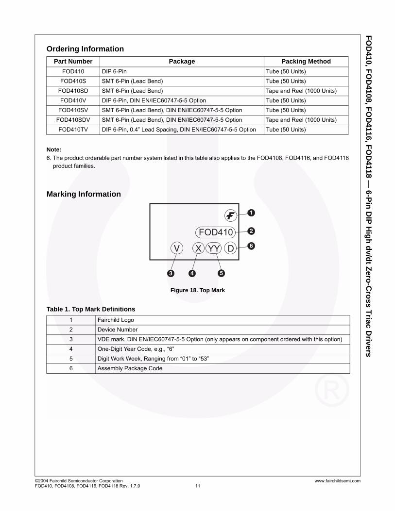
Ordering Information
Note:
6. The product orderable part number system listed in this table also applies to the FOD4108, FOD4116, and FOD4118 product families.
Marking Information
Figure 18. Top Mark
Table 1. Top Mark Definitions
Part Number Package Packing Method
FOD410 DIP 6-Pin Tube (50 Units)
FOD410S SMT 6-Pin (Lead Bend) Tube (50 Units)
FOD410SD SMT 6-Pin (Lead Bend) Tape and Reel (1000 Units)
FOD410V DIP 6-Pin, DIN EN/IEC60747-5-5 Option Tube (50 Units)
FOD410SV SMT 6-Pin (Lead Bend), DIN EN/IEC60747-5-5 Option Tube (50 Units)
FOD410SDV SMT 6-Pin (Lead Bend), DIN EN/IEC60747-5-5 Option Tape and Reel (1000 Units)
FOD410TV DIP 6-Pin, 0.4” Lead Spacing, DIN EN/IEC60747-5-5 Option Tube (50 Units)
1 Fairchild Logo
2 Device Number
3 VDE mark. DIN EN/IEC60747-5-5 Option (only appears on component ordered with this option)
4 One-Digit Year Code, e.g., “6”
5 Digit Work Week, Ranging from “01” to “53”
6 Assembly Package Code
1
2
6
43 5
V
www.onsemi.com1
ON Semiconductor and are trademarks of Semiconductor Components Industries, LLC dba ON Semiconductor or its subsidiaries in the United States and/or other countries.ON Semiconductor owns the rights to a number of patents, trademarks, copyrights, trade secrets, and other intellectual property. A listing of ON Semiconductor’s product/patentcoverage may be accessed at www.onsemi.com/site/pdf/Patent−Marking.pdf. ON Semiconductor reserves the right to make changes without further notice to any products herein.ON Semiconductor makes no warranty, representation or guarantee regarding the suitability of its products for any particular purpose, nor does ON Semiconductor assume any liabilityarising out of the application or use of any product or circuit, and specifically disclaims any and all liability, including without limitation special, consequential or incidental damages.Buyer is responsible for its products and applications using ON Semiconductor products, including compliance with all laws, regulations and safety requirements or standards,regardless of any support or applications information provided by ON Semiconductor. “Typical” parameters which may be provided in ON Semiconductor data sheets and/orspecifications can and do vary in different applications and actual performance may vary over time. All operating parameters, including “Typicals” must be validated for each customerapplication by customer’s technical experts. ON Semiconductor does not convey any license under its patent rights nor the rights of others. ON Semiconductor products are notdesigned, intended, or authorized for use as a critical component in life support systems or any FDA Class 3 medical devices or medical devices with a same or similar classificationin a foreign jurisdiction or any devices intended for implantation in the human body. Should Buyer purchase or use ON Semiconductor products for any such unintended or unauthorizedapplication, Buyer shall indemnify and hold ON Semiconductor and its officers, employees, subsidiaries, affiliates, and distributors harmless against all claims, costs, damages, andexpenses, and reasonable attorney fees arising out of, directly or indirectly, any claim of personal injury or death associated with such unintended or unauthorized use, even if suchclaim alleges that ON Semiconductor was negligent regarding the design or manufacture of the part. ON Semiconductor is an Equal Opportunity/Affirmative Action Employer. Thisliterature is subject to all applicable copyright laws and is not for resale in any manner.
PUBLICATION ORDERING INFORMATIONN. American Technical Support: 800−282−9855 Toll FreeUSA/Canada
Europe, Middle East and Africa Technical Support:Phone: 421 33 790 2910
Japan Customer Focus CenterPhone: 81−3−5817−1050
www.onsemi.com
LITERATURE FULFILLMENT:Literature Distribution Center for ON Semiconductor19521 E. 32nd Pkwy, Aurora, Colorado 80011 USAPhone: 303−675−2175 or 800−344−3860 Toll Free USA/CanadaFax: 303−675−2176 or 800−344−3867 Toll Free USA/CanadaEmail: [email protected]
ON Semiconductor Website: www.onsemi.com
Order Literature: http://www.onsemi.com/orderlit
For additional information, please contact your localSales Representative
© Semiconductor Components Industries, LLC


![(LQEDXDQOHLWXQJ ,QVWDOODWLRQ 0DQXDO · 6fkxw]duw ,3; /xiwyroxphqvwurp $86 - pñ k Ätxdvl³-vwxihqorv ]zlvfkhq xqg pñ k](https://img.pdfslide.tips/doc/110x75/5b149f367f8b9a437c8dee05/lqedxdqohlwxqj-qvwdoodwlrq-6fkxwduw-3-xiwyroxphqvwurp-86-pn-k-aetxdvl-vwxihqorv.jpg)

![1. Excel. µ file- µ « . µ µ µ µ µ µ µ µ ; µµ ; µµ µ Excel Word; µ µ µµ ;[ ] µ , µ µ µ](https://img.pdfslide.tips/doc/110x75/5e1c0fbb3625a8105f7711f5/1-excel-excel-word-.jpg)

![ëÑ pÑ}ªÑgpѤc p pÑ C] SpÕÕpÑÕ ] pѤ - Osnabrück](https://img.pdfslide.tips/doc/110x75/62860dbee5789e26260aeff1/-pgpc-p-p-c-spp.jpg)