Embed Size (px)
Citation preview
uPD7220
GDC
DESIGN
MANUAL
Version 3
TABLE OF CONTENTS
CHAPTER 1
CHAPTER 2
INTRODUCTION •••••••••••••••••••••••••••••••••••••••• 1
1 1.1
1.2
Features •••••••••••••••••••••••••••••••••••••••
System Considerations •••••••••••••••••••••••••• 2
GDC GRAPHICS MEMORY INTERFACE ••••••••••••••••••••••• 3
3
4
4
5
5
6
6
6
7
7
7
8
9
2.1 Introduction •••••••••••••••••••••••••••••••••••
2.2
2.3
2.4
2.5
2.6
Clocking the GDC •••••••••••••••••••••••••••••••
2.2.1 2xWCLK •••••••••••••••••••••••••••••••••• Bus Control Signals ••••••••••••••••••••••••••••
2.3.1 Address Latch Enable Signal ALE (RAS/) ••
2.3.2 Data Bus Input Enable DBIN/ ••••••••••••• The Multiplexed Address and Data Bus •••••••••••
2.4.1 AD~ through AD15 •••••••••••••••••••••••• 2.4.2 A16 and A17 ••••••••••••••••••••••••••••• Additional Signals ••••••••••••••••••••••••••••• 2.5.1 2.5.2 Memory
2.6.1 2.6.2 2.6.3
Horizontal Sync ••••••••••••••••••••••••• Blanking •••••••••••••••••••••••••••••••• Cycles in the Video Display Memory •••••• Basic Memory Cycle Timing ••••••••••••••• Dynamic Memory Timing Signals ••••••••••• Display Cycle Timing ••••••••••••••••••••
10
11
14 2.7 Display Zoom Hardware ••••••••••••••••••••••••• , 16
2.7.1 2.7.2
2.8 Wide
2.8.1 2.8.2 2.8.3 2.8.4
Introduction •••••••••••••••••••••••••••• 16 Zoomed Display Cycle Timing and
Implementation ••••••••••••••••••••••••• 17 Display Access Mode ••••••••••••••••••••••• 20
Introduction •••••••••••••••••••••••••••• 20 Structure of Display Memory ••••••••••••• 21 Ultra High Speed Video Hardware ••••••••• 21 32-Bit Characters ••••••••••••••••••••••• 22
2.9 The Image Bit •••••••••••••••••••••••••••••••••• 22 2.9.1 Introduction •••••••••••••••••••••••••••• 22 2.9.2 Timing Details •••••••••••••••••••••••••• 24
2.9.3 The Image Bit in Graphics Mode •••••••••• 25 2.10 Smooth Horizontal Panning •• ~ •••••••••••••••••• _ 25 2.11 Read-Modify-Write Display Memory Cycles •••••••• 27
i
CHAPTER 3 READ-MODIFY-WRITE LOGIC ••••••••••••••••••••••••••••• 33 3.1 Overview ••••••••••••••••••••••••••••••••••••••• 33 3.2 Logic Unit ••••••••••••••••••••••••••••••••••••• 35 3.3 Figure Drawing Logic (FDL) and Mask Register ••• 41 3.4 Pattern Register Logic •••••••••••••••••••••••••. 43
CHAPTER 4 FIGURE DRAWING •••••••••••••••••••••••••••••••••••••• 45 4.1 Introduction ••••••••••••••• ~ ••••••••••••••••••• 45 4.2 Dot Addressing During Figure Drawing ••••••••••• 45
4.3 Display Memory Architecture •••••••••••••••••••• ·46 4.3.1 Overview •••••••••••••••••••••••••••••••• 46 4.3.2 Modes of Operation •••••••••••••••••••••• 47 4.3.3 Linear Address Space Concept •••••••••••• 47
4.4 Display Memory Contents •••••••••••••••••••••••• 49 4.5 Specifying a Pixel Address in "Display Memory ••• 50
4.5.1 EAD and dAD Definitions ••••••••••••••••• 50 4.5.2 X-Y to Memory Address Conversion •••••••• 50
4.5.2.1 Definitions •••••••••••••••••••• 50 4.5.2.2 Upper Left Corner •••••••••••••• 51 4.5.2.3 Word Addresses on Display
Memory •••••••••••••••••••••••• 51 4.5.2.4 Finding the Word Addresses
Given the X, Y Coordinates •••• 52 4.5.2.5 Finding the DOT Addresses •••••• 52 4.5.2.6 Calculation Considerations ••••• 53
4.5.2.7 Other Coordinate Systems ••••••• 53 4.5.2.8 Display Memory Organization •••• 54
4.6 Drawing Directions............................. 55 4.7 Initial Drawing Direction •••••••••••••••••••••• 56 4.8 The Digital Differential Analyzer •••••••••••••• 59
4.9 The Figure Drawing Process ••••••••••••••••••••• 4.10 Preparing the GDC for Figure Drawing ••••••••••• 60
4.11 FIGS Parameters for Figure Dr.awing ••••••••••••• 62
4.12 FIGS Command Type Parameter •••••••••••••••••••• 63 4.12.1 Introduction ••••••••••••••••••••••••••• 63 4.12.2 RMW Operation Start Commands ••••••••••• 64 4.12.3 Correlation Between Command and
Figure Type ••••••••••••••••••••••••••• 64 4.13 vector Drawin-g ••••••••••••••••••••••••••••••••• 65 4.14 vector Drawing Example ••••••••••••••••••••••••• 69
4.15 vector Drawing Algorithm ••••••••••••••••••••••• 70
ii
4.16 Arc and Circle Drawing ••••••••••••••••••••••••• 73 4.17 Arc Drawing Cursor Positioning ••••••••••••••••• 74
4.18 Calculating Arc FIGS Parameters •••••••••••••••• 75
4.19 Rectangle Drawing •••••••••••••••••••••••••••••• 78
4.20 Area Filling and Graphics Character Drawing •••• 79 4.21 DMA Transfers •••••••••••••••••••••••••••••••••• 84
4.21.1 4.21.2
4.21.3
4.21.4
Introduction ••••••••••••••••••••••••••• 84 Preparing for a DMA Transfer ••••••••••• 84
DMA Examples ••••••••••••••••••••••••••• 86 Partial Word DMA Writes •••••••••••••••• 88
4.22 Successive Address Accesses •••••••••••••••••••• 89 4.23 Word Reading and Writing ••••••••••••••••••••••• 89
4.24 GDC Command Sequence Examples •••••••••••••••••• 91
4.24.1 4.24.2
4.24.3
4.24.4
4.24.5 4.24.6
4.24.7 4.24.8
4.24.9
Introduction ••••••••••••••••••••••••••• 91 Minimum FIFO Load Times •••••••••••••••• Initialization (Master VSYNC Mode,
Graphics Mode) •••••••••••••••••••••••• 91 Display Mode Change •••••••••••••••••••• 92
Blank the Screen ••••••••••••••••••••••• 93 Unblank the Screen ••••••••••••••••••••• 94
Drawing Setup •••••••••••••••••••••••••• Cursor Positioning (Graphics Mode) •••••
Mask Register Loading •••••••••••••••••• 4.24.10 vector Drawing •••••••••••••••••••••••••
4.24.11 Single Dot Writing •••••••••••••••••••••
4.24.12 Arc Drawing ••••••••••••••••••••••••••••
94 94
95 95
96
97
4.24.~3 Area Filling/Graphics Characters
(Random Sizes) •••••••••••••••••••••••• 97
4.24.14 Area Filling/Graphics Characters (8 by 8).............................. 99
4.24.15 Rectangle Drawing •••••••••••••••••••••• 100 4.24.16 Pan and Scroll the Display Window •••••• 10l
4.24.17 Zoom Factor Change ••••••••••••••••••••• 10l 4.24.18 Set Background ••••••••••••••••••••••••• 10l
4.24.19 Multi-Pixel Write •••••••••••••••••••••• 102 4.24.20 Reading Data From the Display Memory ••• 103 4.24.21 DMA Data Writing ........................ 105
4.24.22 DMA Data Reading •••••••••••••••••••••••. 106
iii
CHAPTER 5
CHAPTER 6
4.25 Initializing the GDC ••••••••••••••••••••••••••• 107 4.25.1 4.25.2
Initializing Command Sequence •••••••••• 107 Special Considerations for
RESET Command •••••••••••••••••••••••••• 108
HOST INTERFACE •••••••••••••••••••••••••••••••••••••• 109 5.1 The FIFO Buffer •••••••••••••••••••••••••••••••• 109
5.1.1 5.1.2 5.1.3
5.1.4
5.1.5
Introduction •••••••••• ~ ••••••••••••••••• 109 FIFO Status Bits •••••••••••••••••••••••• 109 FIFO Operation Modes •••••••••••••••••••• 110 Command and Data Transfer
Through the FIFO ••••••••••••••••••••••• 110 Considerations for Testing the status Bits •••••••••••••••••••••••••••• lll
5.2 DMA Interface Hardware ••••••••••••••••••••••••• 112 5.2.1 Introduction.~ •••••••••••••••••••••••••• 112 5.2.2 5.2.3 5.2.4
The Basic DMA Cycle ••••••••••••••••••••• 113 DMA Cycle Minimum Length ••••••••••••••• 114 Timing Considerations for the DMA Transfer ••••••••••••••••••••••••••• 114
VIDEO INTERFACE ••••••••••••••••••••••••••••••••••••• l17 6.1 Video
6.1.1 6.1.2 6.1.3
6.2 Cursor
6.2.1
6.2.2 6.2.3
Timing Calculations •••••••••••••••••••••• 1l7 Introduction •••••••••••••••••••••••••••• 117 Calculating the Parameters •••••••••••••• 1l8 Special Considerations for Interlaced
Video ••••••••••••••••••••••••••••••••••• 130 Display ••••••••••••••••••••••••••••••••• 132 Introduction •••••••••••••••••••••••••••• 133
Wide Display Mode ••••••••••••••••••••••• 133 Cursor Programming Considerations ••••••• 134
APPENDIX A DISPLAY MEMORY ARCHITECTURE BLOCK DIAGRAM •••••••••• 135
APPENDIX BONE-PLANE GDC SYSTEM DESIGN •••••••••••••••••••••••• 136
iv
FIGURES
2.1 Outputting the Display Memory Address ••••••••••••••••••••• 11
2.2 Memory Strobe Generation Logic •••••••••••••••••••••••••••• 12
2.3 Zoom Magnified Display Cycles ••••••••••••••••••••••••••••• 14
2.4 Pipelined Video System (Zoom = 3) ••••••••••••••••••••••••• 15 2.5 Video Register Load Enable Circuit (High Speed) ••••••••••• 16
2.6 2.7
2.8 2.9
2.10 2.11
2.12 2.13
Video Register Load Timing Diagram •••••••••••••••••••••••• 16 Unzoomed Ix Display Cycle Timing •••••••••••••••••••••••••• 17
2x Zoomed Display Cycle Timing •••••••••••••••••••••••••••• 18
Zoom Log i c. • • • • • • • • • • • • • • • • • • • • • • • • • • • • • • • • • • • • • • • • • • • • • •• 19 Mixed Mode Display Addressing, DAD •••••••••••••••••••••••• 24
Horizontal Smooth Scroll Hardware ••••••••••••••••••••••••• 26
RMW Cycle Timing •••••••••••••• 0 •••••••••••••••••••••••••••• 28 RMW Timing Generator ••••••••••••••••••••••••••••••••••••••
2.14a Zoomed Display RMW Cycles (zoom = 2) ••••••••••••••••••••••
28
30
2.14b Zoomed Display RMW Cycles (zoom = 3) •••••••••••••••••••••• 31
3.1 RMW Logic Block Diagram ••••••••••••••••••••••••••••••••••• 34 3.2 Pattern Registr Operation During Different
Logic Functions •••••••••••••••••••••••••••••••••••••••••• 36
3.3 RMW Logic Block Diagram ••••••••••••••••••••••••••••••••••• 37 3.4 3.5a
3.5b
3.5c
3.5d
3.5e
3.5f
4.1
4.2 4.3
4.4 4.5
GDC Figure Drawing Hardware ••••••••••••••••••••••••••••••• 38 RMW Operation with: PATTERNn = 0, MASKn = X,
Logic Operation = 1, 2, 3 •••••••••••••••••••••••••••••• 38
RMW Operation with: PATTERNn = 1, MASKn = 0,
Logic Operation = 1, 2-, 3 •••••••••••••••••••••••••••••• 39
RMW Operation with: PATTERNn = 1, MASKn = 1,
Logic Operation = 1, 2, 3 •••••••••••••••••••••••••••••• 39
RMW Operation with: PATTERNn = X, MASKn = 0,
Logic Operation = 0 •••••••••••••••••••••••••••••••••••• 40
RMW Operation with: PATTERNn = 1, MASKn = 1, Logic Operat.ion = 0 •••••••••••••••••••••••••••••••••••• 40
RMW Operation with: PATTERNn = 0, MASKn = 1,
Logic Operation = 0 •••••••••••••••••••••••••••••••••••• 41
Two-dimensional ArrayDM •••••••••••••••••••••••••••••••••• 47
Cartesian Plane ••••••••••••••••••••••••••••••••••••••••••• 48 Conventional Linear Memory •••••••••••••••••••••••••••••••• 48
Array DM.................................................. 48 Word in Display Memory •••••••••••••••••••••••••••••••••••• 49
4.6 Word Appearance on CRT •••••••••••••••••••••••••••••••••••• 49
v
4.7 4.8 4.9 4.10 4.11
4.12 4.13 4.14 4.15 4'.16 4.17
Display Memory Shown as if Displayed •••••••••••••••••••••• 50 Addresses of Dots within Their Respective Words ••••••••••• 51 Word Addresses on' Display Memory ••••••••••••••• ~ ••••••••• c 51 Direction of Increasing X, Y Values ••••••••••••••••••••••• 52 Or i gin at Lower L eft ••••••••••••• '. • • • • • • • • • • • • • • • • • • • • • • •• 53 Drawing Directions •••••••••••••••••••••••••••••••••••••••• 55 Arc Drawing Directions •••••••••••••••••••••••••••••••••••• 57 Arc Drawing within an Octant •••••••••••••••••••••••••••••• 58 Arc Drawing Across Octant Boundaries •••••••••••••••••••••• 58 Direction Quadrant Definition ••••••••••••••••••••••••••••• 66 Octant Direction Definition ••••••••••••••••••••••••••••••• 66
4.18 vector Drawing Example •••••••••••••••••••••••••••••••••••• 69 4.19 4.20 4.21 4.22 4.23 4.24 4.25 4.26
4.27
Arc Drawing Directions Around a Circle •••••••••••••••••••• 74
Arc Drawing Directions from a Point ••••••••••••••••••••••• 75 Arc Drawing Within an Octant •••••••••••••••••••••••••••••• 75 Determining Arc Length •••••••••••••••••••••••••••••••••• c • 76 Example of Rectangle Drawing •••••••••••••••••••••••••••••• 79 Regular vs. Slanted Graphics Characters ••••••••••••••••••• 81 Zoom 2 Graphics Characters.......... •.••••••••••••••••••••• 81 5-by-7 Character as Seen on the CRT Screen •••••••••••••••• 82
Pattern Drawn Into an Area 19 Wide by 21 High ••••••••••••• 83
5.1 DMA write Timing •••••••••••••••••••••••••••••••••••••••••• 114
5.2 DMA Read Timing ••••••••••••••••••••••••••••••••••••••••••• 114 5.3 DMA Timing Waveforms •••••••••••••••••••••••••••••••••••••• ll5 5.4 System Configuration to Maintain DMA High until
DACK/ Occurs •••••••••••••••••••••••••••••••••••••••••••••. 116 5.5 System Configuration with uPD8257 DMA Controller
to Maintain TI, T2 ~ TCLK •••••••••••••••••••••••••••••••• ~16 5.6 System Configuration for DMA Operation with
Flashless Mode •••••••••••••••••••••••••••••••••••••••••••. 116
5.7 System Configuration for DMA Operation with uPD8237
6.1
A.l A.2
DMA Controller ••••••••••••••••••••••••••••••••••••••••••• l16
Horizontal Timing Relative to Vertical Sync Transitions ••• 13l
Wide Display Cycle Memory Configuration ••••••••••••••••••• 135 4-Plane Display System with Character Mode Option ••••••••• l35
B.l One-Plane System, Part A .................................... 136 B.2 One-Plane System, Part B •••••••••••••••••••••••••••••••••• l37 B.3 One-Plane System, Part C •••••••••••••••••••••••••••••••••• 138
vi
TABLES
4.1
4.2 4.3
4.4 4.5
4.6
4.7
Operations to Address the Next Pixel ••••••••••••••••••••••• 56
Figure Operations •••••••••••••••••••••••••••••••••••••••••• 56 The WDAT Command Format •••••••••••••••••••••••••••••••••••• 61
RMW Logical Operations ••••••••••••••••••••••••••••••••••••• 61 FIGS Parameter Byte 1 •••••••••••••••••••••••••••••••••••••• 63 Figure Type Select Bit Combinations •••••••••••••••••••••••• 63 Allowed RMW Operations ••••••••••••••••••••••••••••••••••••• 65
vii

CHAPTER 1 INTRODUCTION
The uPD7220 Graphics Display Controller (GDe) is an intelligent microprocessor peripheral designed to be the heart of a high-performance raster-scan computer graphics and character display system. Po~itioned between the video display memory and the microprocessor bus, the GDC performs the tasks needed to generate the raster display and manage the display memory. Processor software overhead is minimized by the GDC's sophisticated instruction set, graphics figure drawing, and DMA transfer capabilities. The display memory supported by the GDC can be configured in any number of formats and sizes up to 256K l6-bit words. The display can be zoomed and panned, while partitioned screen areas can be independently scrolled. With its light pen input and multiple controller capability, the GDC is ideal for advanced computer graphics applications.
1.1 Features
• Microprocessor Interface DMA transfers with 8257- or 8237-type controllers FIFO Command Buffering
• Display Memory Interface Up to 256K words of 16 bits Read-Modify-Write (RMW) Display Memory cycles in under 800ns Dynamic RAM refresh cycles for nonaccessed memory
• Light Pen Input
• External video synchronization mode
• Graphics Mode . Four megabit, bit-mapped display memory
• Character Mode 8K character code and attributes display memory
• Mixed Graphics and Character Mode 64K if all characters 1 megapixel if all graphics
• Graphics Capabilities Figure drawing of lines, arc/circles, rectangles, and graphics characters in 800ns per pixel Display l024-by-I024 pixels with 4 planes of color or grayscale Two independently scrollable areas
1
• Character Capabilities Auto cursor advance Four independently scrollable areas Programmable cursor height Characters per row: up to 256 Character rows per screen: up to 100
• Video Display Format Zoom magnification factors of 1 to 16 Panning Command-settable video raster parameters
• Technology Single +5 volt, NMOS, 40-pin DIP
• DMA Capability Bytes or word transfers 4 clock periods per byte transferred
1.2 System Considerations
The GDC is designed to work with a general purpose microprocessor to
implement a high-performance computer graphics system. Through the division of labor established by the GDC's design, each of the system
components is used to the maximum extent through a six-level hierarchy of simultaneous tasks. At the lowest level, the GDC generates the
basic video raster timing, including sync and blanking signals. Part1tioned areas on the screen and zooming are also accomplished at this level. At the next level, video display memory is modified during the figure drawing operations and data moves. Third, display memory addresses are calculated pixel by pixel as drawing progresses.
Outside the GDC at the next level, preliminary calculations are done to prepare drawing parameters. At the fifth level, the picture must be represented as a.list of graphics figures drawable by the GDC.
Finally, this representation must be manipulated, stored, and communicated. By handling the first three levels, the GDC takes care of the high-speed and repetitive tasks required to implement a graphics system.
2
CHAPTER 2 GDC Graphics Memory Interface
2.1 Introduction
The uPD7220 Graphics Display Controller (GDC) interfaces to its display memory using 20 of its 40 pins. The GDC assumes full
responsibility for controlling all aspects of this interface, including generating the raster-scan address sequence, the reading and
modification of display memory data, and coordination of these activities. This interface, as described below, controls a fully
functional video system, but extra hardware can be added to provide more advanced systems with higher performance levels.
The 20 interfacing lines are used for several purposes. The three
operating modes of the GDC vary the use of some of the pins, as will be noted later. Graphics mode pin usage will be described first. Sixteen
pins are used for the bi-directional address and data bus, ADO to ADI5, which forms the heart of the interface. Two lines, Al6 and Al7, output
the top two bits of the display memory address and provide system control signals in operating modes other than Graphics mode. The last
two lines, ALE (or RAS/) and DBIN/, provide the timing and control information necessary to coordinate external hardware with the GDC's bus timing.
In addition to these 20 lines, the Blanking and Horizontal Sync outputs are also involved in the display memory interface. The
assertion of Blanking is coordinated with the bus cycle timing and type so that only active display information reaches the CRT screen.
Horizontal Sync is used in one of the display modes to key the multiplexing of system control information over the A16 and Al7 pins during horizontal retrace blanking.
Although the display memory interface provides addresses during the display raster-scanning process, it is not involved in the video pixel
rate operations. The frequencies involved are often too high for any MOS LSI device. Therefore, external hardware must handle the
parallel-to-serial conversion of display memory words into pixels, etc. Although the GDC supports zoomed display magnification and 32-bit wide
display cycle accesses (twice the normal 16 pixel width), external hardware must be designed to support these capabilities. For
capabilities beyond these basic ones, additional external hardware can
3
be used to add many features such as dual ported memory, smooth horizontal panning, and video look-up tables~ This partitioning of functions between the GDC and external hardware makes possible a great deal of design flexibility.
2.2 Clocking the GDC
A single clock drives the GDC and all the internal logic of the IC and is used as the basis for display timing generation. This TTL-compatible input runs at twice the memory display cycle rate. Therefore, with a 5 MHz clock, normal display cycles will take 400 nsec
(two clock cycles of 200 nsec each). During this time, either 16 or 32 bits will be accessed from video display memory and loaded into the
parallel-to-serial video shift registers. The clock input pin of the GDC is labeled "2xWCLK" to emphasize that two clock cycles are used for each non-zoomed display memory cycle. Note that the frequency of this clock signal will be determined by the requirements of the video display CRT unit. 'A low-speed CRT, for example, will need video data generated at a rate below the maximum.
Other memory cycle types use different numbers of clock cycles but are always a multiple of two clock periods. This fundamental time period will be referred to as a "word time-. Read-modify-write memory cycles use four cycles of the 2xWCLK when the display zoom factor is 1 or 2. For zoom factors greater than two, RMW cycles are extended to the same length as the lengthened zoomed display cycles. Zoom-magnified display cycles use two extra clock periods per zoom factor increment.
The 2xWCLK input is easy to drive with a TTL signal. The minimum high level voltage required for a logic HIGH on this input is 3.9V. The maximum low voltage which will be interpreted as a logic LOW is 0.6V. In order to ensure a good noise immunity margin in the high state, a pull-up resistor can be used to achieve voltages in excess of 3.9V, and the driving TTL output can be lightly loaded to provide extra low state , noise immunity. All other GDC inputs accept the standard TTL levels of
0.8V and 2.0V and require no special provisions.
4
2.3 Bus Control Signals
2.3.1 Address Latch Enable Signal ALE (RAS/)
The Address Latch Enable Signal, ALE, identifies the start of a memory cycle. This is important because the 2xWCLK clock is running at
twice the fastest memory cycle rate, making it impossible for external circuitry to predict which clock cycle will be the first one of the upcoming memory cycle. Also, the differing lengths of blanked, active display, zoomed display, and read-modify-write (RMW) memory cycles demand a constantly adapting determination of the first clock cycle. Since ALE always marks the start of a new memory cycle, it must be used to synchronize the external circuitry to the GDC's bus timing.
The falling edge of ALE indicates the first clock cycle of a new memory cycle and the availability of the memory address on the ADO through ADIS pins and A16 and A17. External circuitry should begin the row and column address strobing of dynamic RAMs after the occurrence of
this edge. The precharge time required by the RAMs can often be provided by the ALE high time which precedes this falling edge. Indeed, the timing of this signal may be used as the RAS/ strobe, fed directly to the display memory RAMs. In any case, the required external hardware will be simple, but the detailed implementation will be application dependent. For example, in high speed systems it may be impossible to finish the RAS and CAS sequence before the address supplied by the GDC begins to disappear (in preparation for data inputting during RMW cycles). In this case it will be necessary to latch the column address component to ensure that data hold times are met at the RAMs, relative
to the strobes. Static RAM display memories will have different timing requirements than dynamic RAM designs.
The ALE signal must also be used to control the loading of the Video
Shift registers. External hardware should load the shift registers with the data accessed from the RAMs at the endo of the second clock cycle. This can be allowed to happen regardless of memory cycle type, since the GDC will assert its blanking output pin to suppress any non-active display access such as RMW, and retrace cycles.
5
2.3.2 Data Bus Input Enable DBIN/
The assertion of the DBIN/ output identifies the time the GDC will accept the data read from the RAMs during RMW cycles. The GDC will
input the data found at its AD lines near the end of this DBIN/ low period and use it during the modify operation to generate the data which will be written back into the originally specified memory locatin late in the RMW cycle. The resulting data is output without further indication by the GDC, so that external logic must generate the necessary write pulse and any bus turn-around control signals. These signals can easily be generated using the DBIN/ signal from the GDC. How the DBIN/ signal is used to generate these signals depends on the
particular system architecture under consideration. The DBIN/ assertion is the only direct way to differentiate an RMW cycie from other memory cycles.
2.4 The Multiplexed Address and Data Bus
2.4.1 ADO through ADIS
The sixteen pins ADO to ADIS form the main pathway between the GDC and the video display memory for both address and data information.
During every memory cycle, regardless of type, the low 16 bits (13 bits in character mode) of an address in the display memory are sent out over these pins. Together with the Al6 and Al7 output-only pins, up to an l8-bit address is provided. During read-modify-write (RMW) cycles, the l6-bit data read from the display memory is then input over these lines to the GDC in response to the DBIN/ signal. Later in the RMW cycle, the resulting data is output back to the display memory over this same pathway.
The AD13 to ADIS pins are used differently when the GDC is operated
in the "coded characters only" mode. The low significance three bits of the GDC's internal line counter are output instead of the top three bits
of address and data information. The lower thirteen AD lines are used as ~escribed above, thereby limiting the display memory to 8K l3-bit words. In coded 'character display applications this is many pages of text and many attribute bits. By making direct use of the GDC's internal line counter to drive the character generator, the external hardware can be very simple.
6
2.4.2 Al6 and Al?
These two output-only pins are used differently in each of the GDC's operating modes. In Graphics mode, they are used in conjunction with the ADO to ADl5 pins to provide an IS-bit address in display memory. In
Coded Character mode, AI? outputs the cursor signal while Al6 supplies the most significant bit of the line counter. In Mixed mode, they are
multiplexed so that during horizontal sync pulses, Al? signals whether the upcoming raster line should be interpreted as bit-mapped graphics or
characters, and Al6 outputs the external line counter clear pulse. During the active display time, AI? indicates the cursor position (in"a
character area), and Al6 follows the attribute blinking timing.
The values at these pins can change during the first clock cycle of
the memory cycle and the fourth clock cycle of an RMW cycle. During
Mixed mode operation, these values, which are available during the
horizontal sync (HSYNC) period, can be loaded into a flip-flop which is
clocked by HSYNC's trailing edge. If the external character generator line counter is implemented with a ?4LSI63, the clock to the counter can be HSYNC inverted, and Al6 can be inverted to drive the counters low true, synchronous clear input (or a ?4LSI61's load input if its parallel
inputs are all zeros). In this way the counter will be incremented at the end of every raster-line's HSYNC pulse except for the first line of
each new character row, when it will be cleared.
In Graphics mode, the Al6 and AI? address values become stable shortly after the start of the memory cycle, and stay stable through the
rest of the cycle until the fourth clock cycle of an RMW cycle. They should be used with latching to drive the select inputs of the decoders
which are used to steer the DBIN and WE pulses to the display memory system. In multiplane systems, A16 and Al7 can be used for selection of
one of four planes during an RMW cycle.
2.5 Additional Signals
2.5.1 Horizontal Sync
The horizontal sync (HSYNC) output indicates the time during the raster-scanning sequence when the CRT's beam is to start its retrace
back to the left side of the screen. The GDC provides a very flexible
7
programming format to allow both its position and width to be specified to one word time (which is the same as two clock cycles).
HSYNC is meaningful to the display memory interface in two ways. First, as mentioned above, it signals the time when the Al6 and AI? pins are being multiplexed during the Mixed mode of operation. Second, the memory cycles during HSYNC pulses are used by the GDC to output the
dynamic RAM refresh addresses over the lower eight AD lines. This function can be enabled or disabled by the RESET command. The refresh address is supplied from the GDC's internal a-bit refresh counter. Since these memory cycles are differentiated from all others by occurring during HSYNC, RAS-only refresh cycles can be easily generated for all RAMs with a few gates. This is important for systems in which the RAMs for one plane have their outputs tied together to drive individual bit lines (i.e., 32 16K RAMs form a 32K by 16 bit plane). Some systems will be designed with only one group of RAMs per plane (one RAM per bit) and will therefore not have outputs tied together (i.e., 16 64K RAMs form a 64K by 16 bit plane). For these systems there is no need to suppress CAS and force RAS for all RAMs during HSYNC periods, since there will be no bus contention and all RAMs will already be getting every RAS.
2.5.2 Blanking
The blanking output from the GDC signals when an active display cycle is occurring so that external hardware can pass the information accessed from display memory to the CRT display. Any other type of
memory cycle should be blanked before the video information reaches the CRT.
In either coded-character or bit-mapped graphics applications, the data word fetched from memory will be loaded into a register as the first step in the generation of the serial video stream that is eventually sent to the the CRT display unit. Often this process will take one or more display pixels, depending on the design. For graphics,
this first register is often a shift register which does a paTallel-to-serial conversion to produce the video serial pixel stream. Further pipeline processing hardware can be added for gray-scale capability and look-up-tables, for example. For coded characters, the first register often holds the data while a character generator is accessed. A shift register then converts the character generators'
a
output from parallel to serial form, which in turn feeds the attribute logic. Of course, along each of these video pipelines the video data is
held in registers which introduce synchronous delays. The blanking signal from the GDC must be kept aligned with the data in the video
pipeline until it is ANDed with the video data, so that only valid data reaches the display screen. This is easily accomplished if the blanking
signal experiences the same synchronous delays as the video data before
the point where the aligned blanking signal is combined with the video
data to allow it to force black on the screen during blanked intervals.
Given synchronously aligned blanking, there is no reason to suppress non-active display cycle loads of the video pipeline since they will
automatically be blanked by the GDC anyway. This feature contributes to a simple interface between the GDC and the display memory.
2.6 Memory Cycles in the Video Display Memory
The main role of the GDC is to manage the video display memory
during both the modification of data in the memory and the raster-scanning process. By giving the responsibility for both of these
competing processes to the GDC, memory cycle allocation can be readily handled. The determination of the next memory cycle type is done by the
GDC via a decision process that includes inputs from the host microp~ocessor at initialization time and internal status including the video Sync Generator and the Command Processor. The result is a smoothly operating display system which provides the user with a great
amount of flexibility in configuring his or her system, and with effective utilization of the display memory's bandwidth.
For the first time in a single LSI device, management of these two
competing tasks, data modification and video display, can be accomplished automatically with no external hardware. In the past this arbitration and switching process required a dual-ported display memory or DMA hardware. Although these options are still open to the GDC system designer, they are no longer the only choices. The GDC will modify display memory at any time during the raster-scanning process for maximum writing speed, or it can be configured by software to do the
modify operations only during the horizontal and vertical flyback times.
By not doing RMW cycles during the active display portion of the raster, no disturbances are visible on the screen. The price paid for this is a lower drawing speed.
9
For those who want high speed drawing wit,h no display disturbances, a dual-ported display memory and two GOCs can be used. The first GOC does nothing but raster-scanning display cycles, while the second GOC does all the drawing. External TTL hardware th~n interleaves their
accesses into the display memory. The two GOCs must use the same clock (or a multiple of the same clock) so they will stay cycle-aligned, and the display memory must have a bandwidth high enough to support both GOCs· accesses without contention.
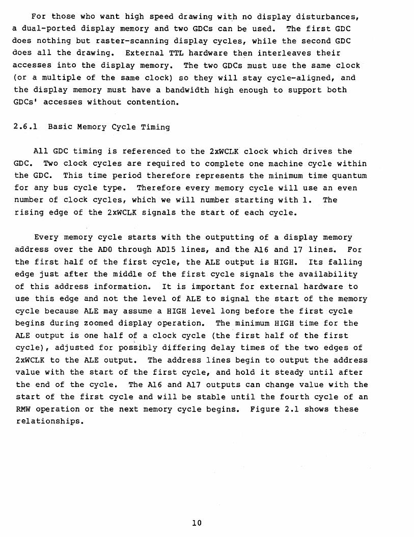
2.6.1 Basic Memory Cycle Timing
All GOC timing is referenced to the 2xWCLK clock which drives the GOC. Two clock cycles are required to complete one machine cycle within the GOC. This time period therefore represents the minimum time quantum for any bus cycle type. Theref~re every memory cycle will use an even number of clock cycles, which we will number starting with 1. The
rising edge of the 2xWCLK signals the start of each cycle.
Every memory cycle starts with the outputting of a display memory address over the ADO through AOlS lines, and the Al6 and 17 lines. For
the first half of the first cycle, the ALE output is HIGH. Its falling edge just after the middle of the first cycle signals the availability
of this address information. It is important for external hardware to use this edge and not the level of ALE to signal the start of the memory
cycle because ALE may assume a HIGH level long before the first cycle begins during zoomed display operation. The minimum HIGH time for the ALE output is one half of a clock cycle (the first half of the first , cycle), adjusted for possibly differing delay times of the two edges of
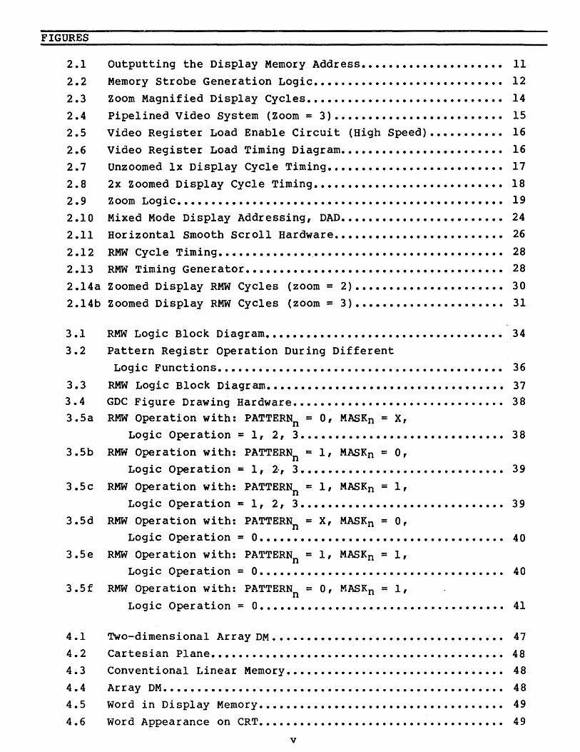
2xWCLK to the ALE output. The address lines begin to output the address value with the start of the first cycle, and hold it steady until after the end of the cycle. The Al6 and Al7 outputs can change value with the start of the first cycle and will be stable until the fourth cycle of an RMW operation or the next memory cycle begins. Figure 2.1 shows these relationships.
10
01 02
2xWCLK ~ ,'--_--II
ALE
AD~ to 15
A16 & 17 -==:::x __________ _
Figure 2.1 Outputting the Display Memory Address
Note that the AD lines return to the high-impedance state at the end of
the first clock cycle regardless of the memory cycle type.
At this point there is no way to tell explicitly if this memory cycle is a display cycle, a read-modify-write cycle, a zoomed display
cycle, or a blanked retrace cycle. In fact, until.the middle of the second cycle, neither ALE or DBIN/ gives any indication of the type of cycle that is in progress. There is normally no need to know the cycle type at this time in the cycle. Regardless of the cycle type, the
addresses generated by the GDC is directed to the display memory.
2.6.2 Dynamic Memory Timing Signals
The larger display memories used for bit-mapped graphics encourage the use of low-cost dynamic memory. Although somewhat more complex to
control than static memory, the cost-per-bit savings of dynamic memory quickly offset the cost of the extra TTL drive hardware. The economics
of a display memory as large as the GDC can control (512K bytes) require the use of dynamic RAMs. with this reality in mind, the GDC was
designed to make this interface as easy as possible.
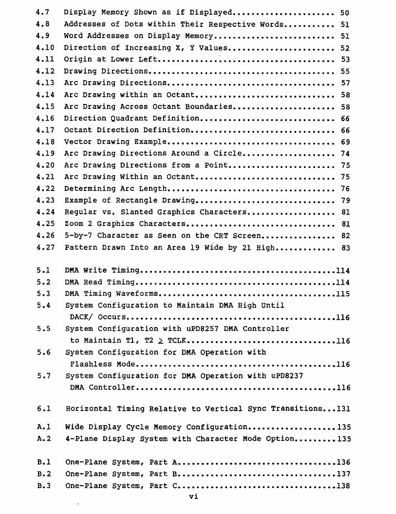
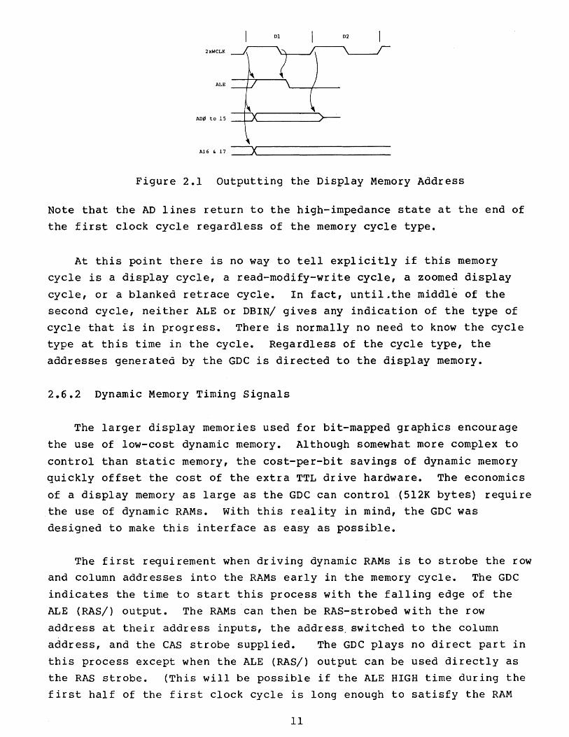
The first requirement when driving dynamic RAMs is to strobe the row and column addresses into the RAMs early in the memory cycle. The GDC
indicates the time to start this process with the falling edge of the ALE (RAS/) output. The RAMs can then be RAS-strobed with the row
address at their address inputs, the address. switched to the column address, and the CAS strobe supplied. The GDC plays no direct part in
this process except when the ALE (RAS/) output can be used directly as the RAS strobe. (This will be possible if the ALE HIGH time during the first half of the first clock cycle is long enough to satisfy the RAM
11
precharge time requirement). These timing signals can be generated with a few TTL packages by using the high frequency oscillator signal which is running eight times faster than a 2xWCLK clock cycle, for example.
More than likely, there is enough timing resolution using the pixel
clock to drive a digital delay shift register which is following the GDC's ALE output. Simple gating can then be used to generate the RAS and CAS strobes and the address select control signal.
GDC
ALE (RAs)
SOl Oll-----+----L-~
74S 194 021-----+--<.,.;-.........
Shift Register U 03t----,
04.----+----r------....
Pixel-CLK -----'
RCM-ADR-SEL
Circuitry will Vary with Application Requirements
Figure 2.2 Memory Strobe Generation Logic
Looking at the overall framework these signals must work within, the main constraint is to have the output data from the RAMs available and set up at the video shift register's inputs at the end of the second clock cycle. The timing requirement for RMW cycle read data is more relaxed than for display cycles and requires no extra hardware when the
DBIN/ output timing can be used directly. During RMW cycle write periods, the WE pulse can often be generated from 2xWCLK timing without any pixel rate clocking. Each display system design must be evaluated individually to ensure that all the timing requirements are met before
the particular timing generator can be finalized. The tremendously wide range of applications suitable for the GDC ensures that no one design will cover all situations.
The second requirement when using dynamic RAMs is to make sure that all row addresses within each RAM are accessed during each RAM refresh peIiod. In some cases where the display is not zoomed and large area DMA accesses are not made in the display memory, the raster-scanning process itself will be sufficient to maintain dynamic RAM refresh. In many applications, however, the raster-scanning process will be
interrupted for too long (by figure drawing, DMA transfers, or zoomed
12
display) to keep the RAMs refreshed. For these situations, the GDC has
an a-bit counter that can generate successive refresh addresses on the least significant AD lines during HSYNC time, if so programmed. Using
this facility, an arbitrarily complex display memory structure can be implemented using multiple RAM pages and planes and still maintain
dynamic RAM refresh for all the devices.
Display memory can be organized in two ways. When using "by one" RAMs such as l6K-by-l or 64K-by-l devices, the minimum group of RAMs is
16 devices with each RAM storing one bit of the GDC's l6-bit word. These groups can be organized so that, first, they share a RAM data output bus to form a bigger linear range of addresses, and second, their outputs can be kept separate and used with independent bus buffers and
video shift registers. The first technique, paging, is used to make a bigger display memory than one group of RAMs can provide, while the second technique, using planes, provides more bits of information at
each pixel position. Both techniques can be combined in the same system.
The approach used to guarantee that the RAMs get enough refresh is slightly different in each case, although both use the GDC's internal refresh counter. The ultimate concern in both cases is to use these refresh cycles during HSYNC to refresh every RAM. The complication arises when multiple pages of RAMs share the same output bus. To effect refresh, each RAM must be given at least the refresh row address and a
RAS strobe. If no more is done, the outputs will stay in the high-impedance state (if CAS/ has been returned to a HIGH). This forms a "RAS only refresh" cycle with no conflict on the output bus because all RAMs have high-impedance output levels. On the other hand, a normal cycle in a multiple page situation would give the RAS strobe only to the addressed RAM page. Some logic must be provided to assert all the RAS
Signals and suppress all the CAS signals during HSYNC refresh cycles in multi-page systems. Single page systems do not need this hardware since
there is no danger of having multiple RAMs drive the same lines. Neither do multiple plane, single page systems need this extra gating
because all the planes are already RASed and CASed for every cycle, and there are no common outputs.
13
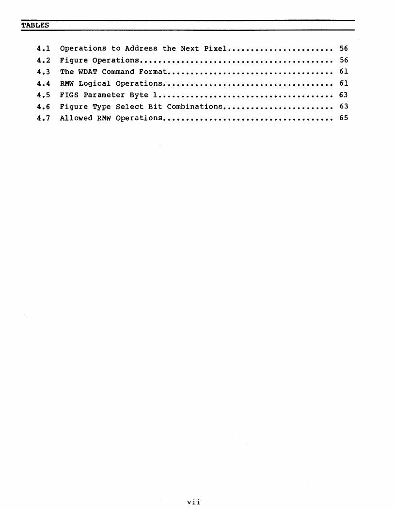
2.6.3 Display Cycle Timing
If the memory cycle is a display cycle, the GDC plays no further
part in the display process after the ALE falling edge. The video pixel clock rates can range as high as 80 MHz in some GDC applications and the
NMOS circuitry in the GDC cannot possibly keep up in the realm of ECL logic. Once the display memory address is output, the GDC will raise its ALE output at the end of the E2 clock cycle. If this is a zoomed display cycle, pairs of clock cycles will then be added to the memory
cycle time to stretch the cycle time while ALE remains high. The lengthened memory access time combined with an externally slowed down
video shift register clock will produce the zoom magnification effect.
Two clock cycles are used for the display cycle for each zoom factor increment. In other words, two clock cycles are used when zoom factor = 1 (normal video), four cycles are used when zoom = 2, etc.
2xWCLK
I Ani' to 15 ::x )
I El I E2 I El I Zoom Ix: ~ ALE
I El I E2 I E3 I E4 El I Zoom 2x: -:::J\ I L ALE
I El I E2 E3 E4 I E5 I E6 I El I Zoom 3x: -:::J\ I L ALE
Figure 2.3 Zoom Magnified Display Cycles
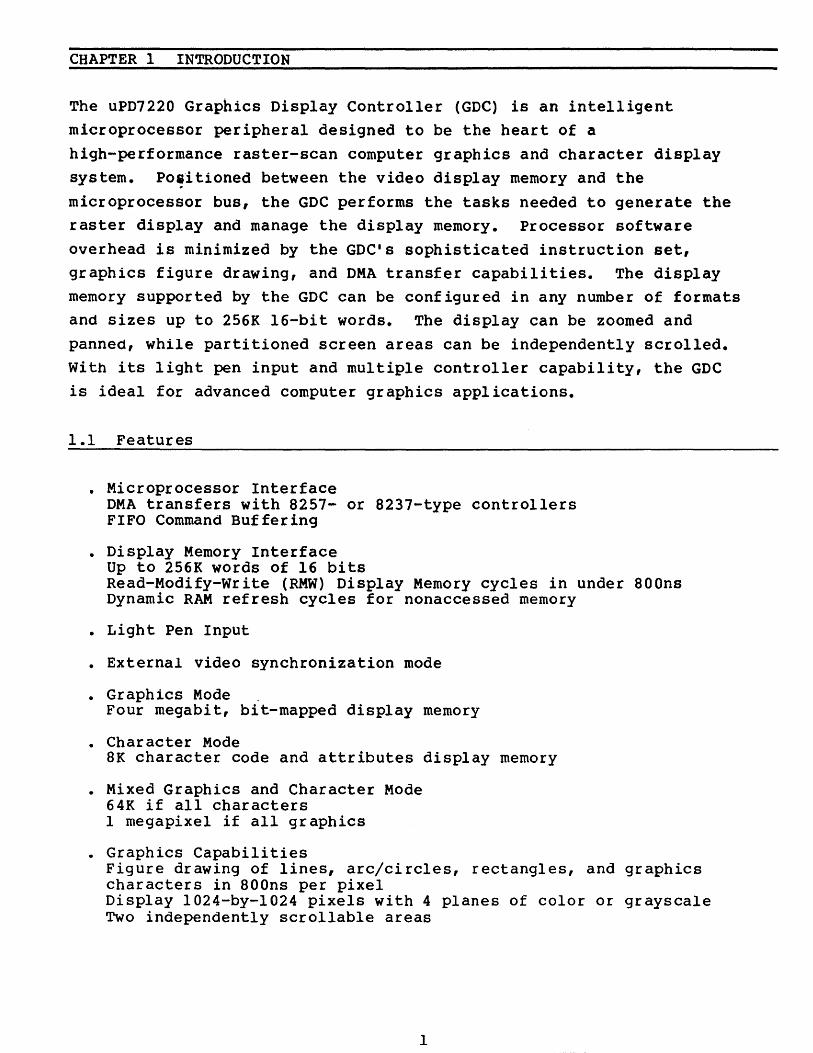
The external video circuitry must be coordinated with the GDC's memory cycle timing. To do this, visualize the overall GDC/video output system as a pipeline with several stages. This is especially important
when zoom operation is planned. The video circuitry is always displaying the most recently accessed video data, while the GDC prepares
the next word of video pixel data. The moment in time when the first video register is loaded with the data just fetched from display memory
is the time when responsibility for processing passes from the GDC to , the video output circuitry for that data. This moment of transference
is the interface between the relatively slow domain of NMOS circuitry, and the relatively high speed world of TTL or ECL. This is also the moment when all the accumulated delays in the GDC/display memory system must be reconciled against the tight tolerance bipolar timing. Finally,
14
this is the moment in time around which the entire video output circuitry needs more data while the last few pixels are going out to the
CRT unit. Figure 2.4 illustrates this principle.
2xWCLl<
Memory Cycle Begins
( (MemOry Data Becomes Available
ALE -~--...-.~ '---./,-------......,'---./
) Data, is Loaded into ~ ~ Video _~_----.~ VIdeo RegIster i X----Output X X'-______ ~,'-. __ _ Words (Zoom 3x)
Figure 2.4 Pipelined Video System (Zoom = 3)
External hardware must be able to find the end of the second cycle
so that the video shift register can be loaded. This is done by using the ALE signal, which will be low at the falling edge of 2xWCLK during
any clock cycle in which the video shift register may be loaded. Some clock cycles in which this is true are not display cycles, but the load
will be a "don't care" action, since the video output from these cycles
will be blanked by the GDC anyway. "Don't care" loads can be found
during RMW cycles or dynamic memory refresh cycles.
The hardware to time the video shift register load can be very
simply implemented. The timing system starts with a clock at the video
pixel rate. This is divided by eight in a counter to generate the 2xWCLK for the GDC. This counter cannot be used to differentiate
between the two clock cycles which make up a display cycle without
reference to the ALE signal. The terminal count of the counter, count 7, during the second 2xWCLK cycle should be used to enable the loading of the video register. By clocking the value of ALE into a flip-flop
with every falling edge of 2xWCLK, the flop's Q output will be HIGH at count 7 time only during clock cycles in which the video register may be
loaded. If this flop output is ANDed in a four input gate with the three counter outputs, a load enable signal will be generated to enable
the loading of the video register synchronously. At slower video rates, the carry-out of the counter can be used with a two input gate and it
will still meet the video register's input setup time requirements. Figure 2.5 illustrates this circuit.
15
GOC jJPD7220
ALE (m) ~-----f
2xWCLK -+-_---L-<
o 745163
C~---~--------~--_ counter 74530 VIOEO-REG-LO-EN ~8 B~--------------~ __ ~
A~------------~
Pixel-CLK
Figure 2.5 Video Register Load Enable Circuit (High Speed)
Pixel-CLK
2xWCLK
ALE
LO-Cycle ______ ...i..-_________ ---'.
VIOEo-REG-LO-EN
Figure 2.6 Video Register Load Timing Diagram
2.7 Display Zoom Hardware
2.7.1 Introduction
The uPD7220 GDC can magnify all the information displayed on the CRT screen. It does this zoom magnification by pixel replication, in which each displayed pixel in the display memory is repeated in both the x and y dimensions the number of times which correspond to the zoom factor. Th~refore, for 2x zoom magnification each displayed pixel occupies the area of 4 unzoomed pixels. It is twice as wide and twice as high as an unzoomed pixel. The GDC can generate zoomed displays of any integer zoom factor between I and 16. This capability is especially useful when using large display formats to allow easy viewing of pixel sized
16
details. The zoom option is available only in the bit mode graphic mode of operation.
The GDC supports all the requirements for zoomed display operation except the stretching of individual pixels. This takes place at video
speeds which can be far above the GDC's frequency limitations.
2.7.2 Zoomed Display Cycle Timing and Implementation
An unzoomed (Ix) display cycle uses two cycles of the 2xWCLK clock
signal, Dl and D2. To start the display cycle, the falling edge of the ALE output pin occurs in the middle of the first clock cycle. ALE stays low until the end of the second clock cycle, when it goes high in preparation for the next display cycle. The address is output on the ADO to 15 lines during the entire first clock cycle. The AD lines float during the second clock cycle. The video shift registers are loaded at
the end of the second clock cycle, D2, with the video data just fetched from display memory. Figure 2.7 below shows these relationships.
lx Display Cycle
2xWCLK:
Clock Cycle:
ALE:
)
Video Shift Registers Loaded
Figure 2.7 Unzoomed Ix Display Cycle Timing
The GDC adds two extra clock cycles to the display cycle for each integer increase in the zoom factor. Therefore, 2x zoom magnification would use four 2xWCLK clock cycles, while a 5x zoom factor would specify ten clock cycles. The timing during the first two clock cycles is the same regardless of the zoom factor. For zoom factors of two and above,
the GDC marks time during clock cycles D3 and beyond with its ALE output
high to indicate that the video shift registers should not be loaded during this period.
During the zoom-lengthened display cycles, the video hardware must slow down the video pixel output rate to match the zoom factor used by the GDC. In this way, each individual pixel is stretched by an integer number of pixel periods as it is serialized for the CRT display. The
17
GDC automatically takes care of repeating the horizontal display lines
to effect the vertical magnification.
An easy way to accomplish the stretching of the pixels is to use synchronous video shift registers and control their shift enable and load inputs. This guarantees that the first pixel of each word will be of the same duration as every other pixel of the word. A synchronous
counter can be used as a zoom factor pre-scaler to enable the video shift registers to shfit only when its Carry Ouput (CO) is high. The Zoom Pre-scaler counter is set to count the zoom factor by modules so that, for example, its CO output is high for one pixel time every five
pixel clock periods for 5x zoom operation. When the pre-scaler is loaded with all ONEs, its Co output will always be high and an unzoomed, Ix display will result. The counter load value must be stored by the host microprocessor in a hardware register and must be available
constantly for the pre-scaler.
The RAM timing generator circuit suggested elsewhere in this manual generates the RAS/ and CAS/ waveforms shown in Figure 2.8 below. Higher zoom factors than 2x add more pairs of clock cycles after D4, but there are no transitions during these cycles.
1-------2x Display Cycle ------1
Clock Cycle: Dl 02 D3 D4
\ I \... ,"Eo I I
I I AD'-l5'T
ADR (n) > 1< ADR (n+ll
I RAS:
I I \ /
I I CAS:
I \ II I I I
RAM DO: ( DATA (n) > I I I
VSR OUT: Pixels (n-l) X Pixels (n)
Figure 2.8 2x Zoomed Display Cycle Timing
Note that the memory read cycle takes place while ALE is low. Triggered by the falling edge of ALE, the RAS/ and CAS/ falling edges
start the RAM cycle. The data outputs of the RAMs assume the values of the stored data in time for the end of the D2 clock cycle. The data is
18
then loaded into the video shift registers (VSR). Once ALE has gone high, the RAM precharge time is started by RAS/ going high, and after a sufficient hold time the CAS/ line is brought high to float the RAM DO lines and prepare for the next cycle.
Note that the video shift register (VSR) is loaded at the end of the
D2 clock cycle, as it was at Ix zoom. Although the GDC starts its cycle with the Dl cycle, the video output hardware begins outputting a new
word of video data at the end of D2, regardless of zoom factor. An effective way to think of this relationship is to imagine the GDC anticipating the need for new video data for the video shift register two clock cycles early. It then proceeds to do the proper memory cycle and idles until two clock cycles before the next shift register load.
The moment the video shift registers are loaded is critical in the timing scheme. Because it is the start of the video output hardware
cycle, everything must coordinate at this point. Not only must the shift registers be loaded at just the right moment, but the pixel
stretching pre~scaler counter must be initialized to its load point so
that the first pixel will be stretched the proper amount. This can be done by "ORing" the CO of the Zoom Pre-scaler counter with the video shift register load enable pulse and feeding the low true result into the synchronous load input of the Zoom Pre-scaler (a 7402 into a 74163 for example).
Using the approach outlined above, zoomed displays can be
implemented using little extra logic. One 16-pin DIP houses the Zoom Pre-scaler counter (74x163), the load gate requires 1/4 14-pin DIP
(7402), and the storage register for the hardware zoom factor can use 1/2 of an octal latch (74x273). The zoom logic is diagrammed in Figure 2.9.
VSR-LO-EN
ZOOM-REG-LD
LO CO 74LS273 74x163
OB-3 -- D Q ~-----1 D 00
OB-2 - D Q C OC DB-l-~- D
OB-O- D
Q~----iB OB Q A CLK OA
Pixel-CLK
SHIFT-EN (to Video Shift
Registers)
Figure 2.9 Zoom Logic
19
2.8 Wide Display Access Mode
2.8.1 Introduction
The Graphics Display Controller can be programmed to work with a
double word access in display memory during active display cycles. In Graphics mode, 32 bits of video data are acce~sed simultaneously, instead of the normal 16 bits. Video data rates of up to 80 MHz are then possible using a 5 MHz GDC clock. Note that during read-modify=write cycles, a single 16-bit word is processed by the GDC, regardless of the display cycle mode.
The wide display accesses can also be used in Character mode and Mixed mode. No matter which mode is used, the width of the display access is always two display memory words. Note that with Character mode's l3-bit word width, the Wide Access mode would provide a 26-bit double word display access. To simplify the discussion, reference will be made o~ly to the 16/32-bit accesses of Graphics and Mixed modes.
The GDC supports double word display cycles by generating the address of every second location to be displayed. To find the next word address, the GDC's Display Word Address counter is incremented by two instead of the normal mode's one. External hardware must then access and video serialize both the even and odd words at these successive addresses. It is generally necessary to have separate banks of RAMs for
the even and odd words in display memory so that all 32 output bits can be accessed and loaded into the video shift registers simultaneously.
The Wide Display access mode is controlled by a bit in the Parameter
RAM for each display area. If bit 7 of PRAM bytes 3 or 7 (11 or 15 in character mode) is set, the display address counter will be incremented by two for each display cycle in the corresponding area on the screen.
Wide Display Access mode is useful when generating ultra-high speed
video, and for coded characters, when using up to 32 bits per character , (26 bits in Character mode).
20
2.S.2 Structure of Display Memory
In the straightforward implementation of Wide Display Access mode hardware, each plane of display memory must have two separate banks of
RAMs. The data output pins of each bank must be kept separate to allow
the desired 32-bit accesses in each plane. Each bank of RAMs, two for
each plane, must have its own RMW cycle read buffer and 16 bits of video
shift register. The video shift registers of the even and odd banks of each plane must be tied together to produce a 32-bit shift register.
The decoding of the address from the GDC must use AO to differentiate between the even and odd banks of RAM during RMW cycles. The highest significance address bits then differentiate the planes. During RMW cycles, the bank of RAMs to be enabled onto the bus during DBIN time and then written into is selected using AO and the plane
select bits. During display cycles, the least significant bit and the
plane select bits are ignored while video data is sent to the CRT
screen.
The strobes for each bank of RAMs can be handled similarly to the normal l6-bit access mode. If no banks of RAMS have multiple groups of
RAMs (no outputs tied together), all banks can be RASed and CASed each memory cycle, blanked, active, or RMW. If there are wire-ORed RAMs, it
may be desirable to do RAS-only refresh cycles during HSYNC time so that all RAMs get all the dynamic RAM refresh cycles.
In straightforward systems, the minimum size of a plane of display
memory in Wide Display Access mode is twice the size of a bank of RAMs. If 64K-by-1 RAMs are used, the minimum plane size would be l2SK l6-bit
words. It is possible to use very fast RAMs and make two display accesses during the two 2xWCLK cycles of a GDC display cycle (as short
as 400 nsec). In such a system, both odd and even planes are located in the same 16-bit memory chip set. This would have the advantage of a smaller minimum plane size, but would require more complex control circuitry.
2.S.3 Ultra High Speed Video Hardware
One of the reasons for using the Wide Display Access mode is to
obtain ultra-high video data rates. With a 5 MHz 2xWCLK, the video data rate will be SO MHz, or 12.5 nsec per pixel. At these speeds ECL logic
21
should be used for the video shift registers. The conversion from TTL to EeL levels is easily done at the outputs of the RAMs before loading into EeL shift registers. This technique, although conceptually simple,
requires 32 level translators per plane and a large number of ECL shift registers.
A different approach is to use low speed TTL shift registers at the outputs of the RAMs, which are clocked at a fraction of the output video
rate. Their outputs are converted to EeL levels and loaded into one high speed ECL shift register per plane. The ECL shift register is clocked at the full video data rate. If four 8-bit TTL shift registers are used with a high speed EeL 4-bit shift register, fewer level
converters will be necessary. Of course, the timing circuitry will be somewhat more complicated to support this two-state shift register
configuration. The oscillator and high speed timing must be done at the pixel clock rate and will likely use EeL circuitry.
2.8.4 32-Bit Characters
When very large sets of characters must be displayed with numerous
attributes using a coded character, 16 bits (or 13 bits) per character are often insufficient. The Wide Access mode can be used in these
situations to provide up to 32 bits per character. Conceptually, the two 16-bit halves of each character are accessed by separate RMW cycles. The 32 bits accessed during display cycles are used in parallel by the character generator and attribute logic, along with the character row
line count, to scan out the character. This capability is especially important when displaying oriental character sets or multiple fonts of
characters.
2.9 The Image Bit
2.9.1 Introduction
An Image bit is stored in the GOe's Parameter RAM for each display area partition (bit 6 in PRAM bytes 3,7). The value of the Image bits
" are set with the PRAM command which loads the appropriate Parameter RAM bytes. In general, the value of the Image bit is set at initialization
and remains unchanged as long as the display area type doesn't change. These bits are important in the Mixed mode of operation but have an effect in other modes also.
22
In Mixed mode, a display area's Image bit specifies whether the area is a bit-mapped graphics area or a coded character area. In
differentiating between these area types, several changes occur in the way the GDC operates. First, in a coded character area, the Lines per Row (LR) parameter of the CCHAR command controls the number of times a given line of words is scanned while the Line Counter is incremented. In a bit-map area, each line is automatically scanned only once. Second, in a coded character area, the external circuitry must include a line counter and a character generator. In a bit-map area, the external circuitry must use only a video shift register. The GDC outputs the
value of the Image bit during HSYNC time on the Al7 pin, where it should be loaded into a flop to control the external circuitry. Third, the way
the GDC handles the Pattern Register during RMW drawing cycles differs between the two types of areas. In a bit-map area, the pattern is used one bit at a time, while in a coded character area, all the bits of the pattern are used in each RMW cycle.
The fourth difference is the nature of the information flow to the
screen in each type of area. In a bit-mapped graphics area, 16 pixels are sent to the CRT from each word access. In coded character areas,
each word access gets a character code value which is converted to a character window's width of pixels by an external character generator.
To mix characters and graphics on the same screen, it is desirable to use the same pixel clock rate for both areas and to have a consistent number of pixels on every line, regardless of the type of information being displayed. To make this mixing easier, the GDC assumes that the character windows will be eight pixels wide. (There are no physical limitations here, just compatibility considerations. The GDC can be
used in Mixed mode with some other window width if no graphics will be displayed.) Therefore, two character windows equal one graphics 16
pixel access width.
The GDC needs two 2xWCLK cycles to access a word in display memory. In Mixed mode, one character code and its attributes are accessed during
this minimum cycle time. To make 16 pixel graphics accesses compatible with 8 pixel character accesses, the GDC accesses a new graphics word every four 2xWCLK cycles instead of every two. Therefore, each pair of 2xWCLK cycles equals eight pixel times, regardless of the type of
display area.
23
During initialization, the AW value must be set for the number of 2xWCLK cycle pairs to be displayed, not the number of graphics words.
2.9.2 Timing Details
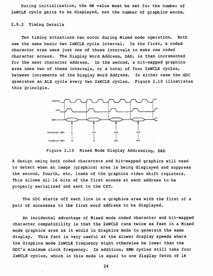
Two timing situations can occur during Mixed mode operation. Both use the same basic two 2xWCLK cycle interval. In the first, a coded character area uses just one of these intervals to 'make one coded character access. The Display Word·Address, DAD, is then incremented for the next character address. In the second, a bit-mapped graphics area uses two of these intervals, or a total of four 2xWCLK cycles, between increments of the Display Word Address. In either case the GDC generates an ALE cycle every two 2xWCLK cycles. Figure 2.10 illustrates this principle.
Character DAD: n n+l n+2 n+3
I I I I Graphics DAD: m m m+l m+l
Figure 2.10 Mixed Mode Display Addressing, DAD
A design using both coded characters and" bit-mapped graphics will need to detect when an image (graphics) area is being displayed and suppress the second, fourth, etc. loads of the graphics video shift registers.
This allows all 16 bits of the first access at each address to be properly serialized and sent to the CRT.
The GDC starts off each line in a graphics area with the first of a pair of accessses to the first word address to be displayed.
An incidental advantage of Mixed mode coded character and bit-mapped character compatibility is that the 2xWCLK runs twice as fast in a Mixed m~de graphics area as it would in Graphics mode to generate the same display. This fact is very useful at the slower display speeds where
the Graphics mode 2xWCLK frequency might otherwise be lower than the GDC's minimum clock frequency. In addition, RMW cycles still take four 2xWCLK cycles, which in this mode is equal to one display fetch of 16
24
pixels, instead of the Graphics mode's two display refresh fetches. Therefore the drawing speed is twice as high in Mixed mode as it is in Graphics mode for the same video display format.
2.9.3 The Image Bit in Graphics Mode
An Image bit set to a ONE will force the "increment every other
display cycle" o~ration for that display area in Graphics mode, like it does in Mixed mode. There is no outputting of the value of this bit
over the A-I? pin during the HSYNC time, so all areas on the screen should be consistent in use of this capability. There is no way to detect where one display area ends and another begins in Graphics mode. If normal Graphics mode operation is desired, the Image bit for each display are must be set to a ZERO, to force an increment of the DAD for each pair of 2xWCLK cycles (one display cycle).
2.10 Smooth Horizontal Panning
The GDC can start raster-scanning the display memory at any word address. It has time to calculate and output the sequence of
addresses necessary to generate the raster-scan video signals. The GDC is not involved with the actual conversion of data accessed from memory into appropriate video signals. Frequencies involved in this process can be as high as 80 MHz, far above the capabilities of NMOS technology. It is often desirable to be able to position the display window at any bit position and not be constrained to word boundaries. External hardware can easily do this at video pixel speeds. When using smooth panning, zoomed display capability is lost.
A straightforwaro approach to smooth panning within word boundaries uses a serial-to-parallel shift register downstream of the normal
parallel-to-serial video shift register. The extra shift register must be a full display cycle width of pixels long. This register is clocked at the video pixel rate and acts like a digital delay line for the serialized video data.
To support smooth panning, the GDC must be programmed for an AW
count two words greater (AW must be an even number) than the desired display width so that, during smooth panning, part of both the first and last words can appear on the screen simultaneously within the desired display window. The Blanking signal from the GDC must then be delayed
25
uy cwo a~sp~ay cyc~e per~oas at tne start ot tne act1ve display area.
Blanking must not be delayed at the end of the line.
The proper delay-line shift register tap must be selected by a
multiplexer which is under the control of the host processor. The tap is advanced pixel by pixel to smoothly pan the display. The first multiplexer input must be connected to the regular video shift register's output. Each following input is connected to the next "more
delayed" delay line shift register output.
The first two active display cycles of each line fill up both shift registers with video data. The first word accessed is lost. The second word accessed occupies all the bits of the delay-line shift register at the moment blanking is removed from the video stream. The particular bit selected by the multiplexer will be the first bit seen on the left edge of the screen. This word will appear to be bit-shifted to the left, behind the blanking edge. This apparent shift will continue across the screen for all the other accesses on the line.
The extra logic necessary to do smooth horizontal panning includes the
delay-line shift register, the multiplexer, and a storage register to hold the delay offset select bits for the multiplexer. (Refer to Figure 2.11).
OM-DATA-15 -14
-13
-12
-11
-10
-9
o
-8 H
Load
OM-DATA-7 -6
-5
-4 -3
-2
-1
-0
A
B
C
o
F
G
H
74LS299
QH
s!n
74LS299
QB
Data from Display Memory
SRI QAI------~
QBI------~
QCI------~
QDI-------i 74LS299
QEI--------f
SRI
QFI-------i
QGI-------i
QAI-------!
QBI-------I
QCI--------f
QDI--------f 74LS299
QEI-------i
QFI--------f
QGI-------i
QH
083 DC2 DBI DDO
Shift Offset Register
Hor izontally 1------.. Shifted
Video Oata
Figure 2.11 Horizontal Smooth Scroll Hardware 26
2.11 Read-Modify-write Display Memory Cycles
Read-modify-write (RMW) cycles are used exclusively by the GDC when
it accesses its display memory for data transfers. Various activities like clearing memory, figure drawing, DMA transfers, and reading and
writing memory contents all use RMW cycles. The timing used is different from display cycle timing. Instead of just supplying an address, the data accessed by the RAS/CAS sequence must be read into the GDC, modified by the GDC's Logic Unit, and the result written back into
the memory. These additional activities are coordinated with the GDC's DBIN/ output and the 2xWCLK. The basic RMW cycle takes four clock
cycles, El through E4. When the display zoom magnification factor is larger than 2, the RMW cycle is extended with ALE HIGH to be the same
length as the zoom lengthened display cycle. It is important to note that an RMW cycle always includes the write back operation, even when the data is not changed but just read. This technique requires only one operating mode for the external hardware, to help keep it simple. The GDC will echo the display memory location's contents as it was read when there are no changes, so that the effect of the write operation will be to leave the display memory location's contents unmodified.
An RMW cycle starts off just like a display cycle, with a falling edge of ALE in the middle of the EI cycle. The display memory address
must be output to the display memory as it always is. In fact, at this point there is no way to tell an RMW cycle from a display cycle. The first difference occurs when DBIN/ goes LOW just after the middle of the E2 cycle. The GDC is thereby requesting the read data from the display
memory to be placed on the AD lines so that it may be input by the GDC at the middle of E3. The DBIN/ LOW period lasts until just after the middle of E3, at which time it returns HIGH. The data is modified during the second half of E3, and the resulting data becomes available on the AD lines with the start of the E4 cycle for write back, and is stable through the end of E4. Note that ALE stays LOW until the end of
E4, and therefore the video shift registers will be loaded at the end of E2 (as in a display cycle), E3, E4. Although these extra loads put
garbage data in the video registers, no harm is done because the video will be blanked during the duration of the RMW cycle. Figure 2.12 illustrates this timing.
27
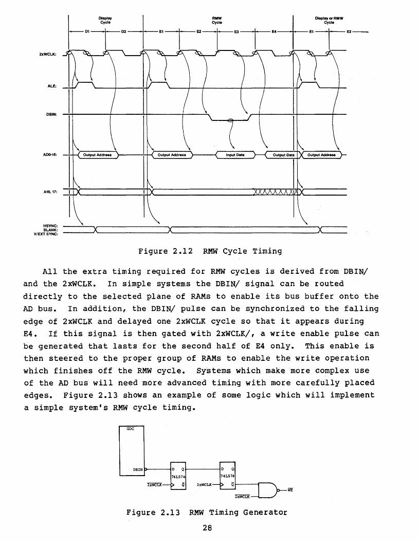
2XWCLK:
ALE:
DBIN:
ADO-15:
A16.17:
HSYNC: BLANK:
VI EXT SYNC:
Figure 2.12 RMW Cycle Timing
All the extra timing required for RMW cycles is derived from DBIN/ and the 2xWCLK. In simple systems the DBIN/ signal can be routed
directly to the selected plane of RAMs to enable its bus buffer onto the AD bus. In addition, the DBIN/ pulse can be synchronized to the falling
edge of 2xWCLK and delayed one 2xWCLK cycle so that it appears during E4. If this signal is then gated with 2xWCLK/, a write enable pulse can be generated that lasts for the second half of E4 only. This enable is then steered to the proper group of RAMs to enable the write operation
which finishes off the RMW cycle. Sistems which make more complex use of the AD bus will need more advanced timing with more carefully placed edges. Figure 2.13 shows an example of some logic which will implement a simple system's RMW cycle timing.
GDC
OSIN D Q ...-----4 74L574
2xWCLK (2 2xWCLK
Figure 2.13 RMW Timing Generator
28
During zoomed display operation, RMW cycles are extended to the same length as display cycles if the zoom factor is 3 or larger. The reason
for this is that RMW cycles and display cycles must interleave during real-time. Since an RMW cycle must be finished once it has begun, and a display cycle cannot be started late, RMW cycles can never be shorter than the display cycles. The GDC automatically stretches the RMW cycles
out to the same length as display cycles, if necessary, by bringing ALE HIGH at the end of E4 as usual and keeping it there until the proper starting time of the next display cycle. Figures 2.l4a and b illustrate this operation.
29
w o
2xWCLK:
\~-----_/ \,-~ ------, \~-------__________ ~~r---\'------
\ __ ----_1
Output Data ADO-15: --:--<C===>-) -----------1~<=~~)---------H{=====)>----{(===>-< I X-----}-
Output Address Output Address Output Address Input Data Output Address
A16,17:::I:X _________________________ ~X'-----------------------------~X--------------______________ +I~X _______ __
BLANK: ==r=\ Ir--------------------------~_,\:===~~~~~ --L,~----------------------------_T------------------------------_T~ ...
Figure 2.l4a Zoomed Display RMW Cycles (Zoom = 2)
w .....
2xWCLK:
o:~::::LJ~i~ ___ \~~~~~~_-_-_-_-_~_/ _____________________________ ~ _____ \~_-_-_-_-_-_-~~---------~~~~~~~~~~_I _____________ ~ _____ \~_-_-__ -_-\~ ______ ...JI
ADO-15: ---+-<:==:J)----------------+-(C==::J~ H )>---------:;....-<{ }-Output Address Output Address Input Data Output Data Output Address
A16,17::J[) ____________________________________________ ~1 X~ ____________________________________________ ~X---------
\'--------Blank: --r-\_-:I __ ~ _______________________________________ _i_..JI
I
Figure 2.14b Zoomed Display RMW Cycles (Zoom = 3)

CHAPTER 3 READ-MODIFY-WRITE LOGIC
3.1 Overview
Read-Modify-Write (RMW) logic is used in every operation involving modification of data in the bit map memory (video buffer). With the GDC, you can perform a logic operation on bits being modified, you can write single or multiple bits in each RMW cycle and, in conjunction with the vector drawing processor, draw a number of patterns in the video memory. The RMW logic operates somewhat differently in the gr·aphic and character modes. Each of the modes will be explained separately.
During a figure drawing process, the GDC must modify a number of bytes in the video memory. In each RMW cycle, only one individual bit
is modified. Since the GDC can access only 16-bit words, each RMW cycle consists of:
1. Read 16-bit data pointed to by EAD 2. Modify the bit pOinted to by dAD 3. Write 16 bits back into video memory
In the character mode, all 13 bits representing the character and
its attributes are modified simultaneously, so that the RMW cycle consists of:
1. Read 13 bits of character (16 bits in mixed mode) 2. Modify some or all bits 3. Write all the bits back into video memory
The block diagram of the RMW logic is shown in Figure 3.1. A few major functional blocks are directly involved in each RMW cycle.
33
~ Figure
/ Drawing Logic
I
r---... <II .....
"- . ~ 0' Pattern
) <II g; Select ~ Logie ... <II
.....
..... ., ~ ~
/1 - 1
I I Mask Register I I
~
/ / ,'\
From Video Memory
8 Data
,
LogiC
Unit
,
, , / ,
Bit
~ /
/ ,
BIT JJ 7"
Figure 3.1 RMW Logic Block Diagram
write Data
To Video Memory
1. FIGURE DRAWING LOGIC: This is the hardware, consisting of a number of adders, shift registers and counters that calculate the address of
each consecutive pixel during the figure drawing process. It controls the bit selection from both the Pattern and Mask Registers.
2. PATTERN REGISTER AND PATTERN SELECT LOGIC: Selects the bits on
which the logic operation will be performed. During the figure drawing process, ~he pointer moves the LSB to MSB of the Pattern Register. If
the bit is set to one, the logic operation takes place. If it is a zero, the bit is not modified. In the character mode, the Pattern
Register holds either the new character or just the few bits that should be modified in the video buffer. Also, during WDAT and DMAW commands, the content of the Pattern Register is written into video memory in 16-bit words.
3. MASK REGISTER: This Register serves as a pointer for figu~e drawing logic to select which bit of the 16-bit word must be modified. As the figure'drawing logic calculates the consecutive addresses of the figure
it is drawing, the Mask Register is shifted right or left accordingly. ,
4. LOGIC UNIT: This logic part does actual RMW data modification. It uses the data from both the Pattern and Mask Registers. Depending on bit patterns, it modifies the l6-bit words from the video memory.
34
Each of these blocks will be discussed in more detail below.
3.2 Logic Unit
Let us start with the Logic Unit hardware. The GDC offers four logic functions:
1. REPLACE
2. COMPLEMENT
3. CLEAR
4. SET
and they are selectable by the MOD field in WDAT and DMAW commands. The operation of each mode is explained in Figure 3.2. The Pattern Register is loaded with a 16-bit data pattern. Before the first pixel of the figure is written into video memory, a pattern register pointer points at bit ~, and MOD Register selects one of the four types of logic operations.
35
First Pixel of the Vector
Pattern Register
Present Memory
Vector with Replace Mode
Complement Mode
Set Mode
Clear Mode
Figure 3.2 Pattern Register Operation During Different Logic Functions
In REPLACE mode, the data in the memory will be replaced with the data in the Pattern Register. In COMPLEMENT mode, any bit that is set to 1 in the Pattern Register will complement the appropriate bits in the pattern the GDC is drawing. In SET or CLEAR modes, only bits that are set to 1 in the Pattern Register will be set and cleared respectively
during the drawing process. ,
As each consecutive pixel is drawn, the Pattern Register pointer is shifted right by one pixel. After reaching bit 15 (MSB), the pOinter
goes back to bit ~ and starts the pattern again. It continues this process for as many pixels as there are bits in memory to be written,
36
regardless of the direction and shape of the figure to be drawn -vector, arc, or rectangle.
Figure 3.3 describes the RMW process. The RMW cycle starts with reading 16 bits of data from the address indicated by EAD. All 16 bits enter a logic unit.
RMW Cycle Counter
CURS dAD Field ~
Logic Uni t
PATTERNn
~ Operations (1) REPLI\CE 1 ) COMPL EMENT 2) CLEAR 3) SET
REPLACE Operation
Q D
RD DATAn
Read Data
16 Bite n = , to 15
W'rite Data
16 BitG
n = , to 15
(one of sixteen shown) RMW Hardware
Figure 3.3 RMW Logic Block Diagram
The SET, CLEAR and COMPLEMENT logic operations work similarly. Only the inputs to MUXl differ. Figures 3.5 a,b, and c show the data path of one of sixteen bits from video memory.
37
A
" ... - .......
I Bus I Buffer ,.;,.;;0 "";0.
L-....
~
EAD Register
GDC Internal Data Bus
............ ~
Pitch Reg ............. !o-
Drawing Control Logic
-.- MSB
M •• k ~ '"H5 '
"'" __ 1000
B
/ !f-Y Register ~
I ~
J ~
if- ~ Adder DIR J - Incr A , - Decr A
MUX
I Load--+ .
J - A Plus B
I'r- II - A Subtr B DC
Shift Left ~ "" ~" y
Operation Bidirec-~
I Shift Right tional D Circular ~
I..--Load Shift If ' .. H A Register ~
I ;a.
I D2 LSB
Dl I DM I
Figure 3.4 GDC Figure Drawing Hardware
PATTERNn= ~
Logical Operation Select
REPLACE -~--.... Operation
RD DATA n
Figure 3.Sa RMW Operation with: PATTERNn = 0, Logic Operation = 1, 2, 3
MASKn = X,
38
L
r
To ~RMW.
Log ~c t Uni
PATTERN = 1 n
LOGICAL OPERATION SELECT
REPLACE --~ Operation
RD DATA n
Figure 3.5b RMW Operation with: PATTERNn = 1, MASKn = 0, Logic Operation = 1, 2, 3
PATTERN 1 n
Logical Operation Select --~
MASK n = 1 -l---1L_ .......
REPLACE -~ __ -' Operation
RD DATA n
Figure 3. 5c RMW Operation wi th: PATTE,RNn = 1, MASKn = 1,
Logic Operation = 1, 2, 3
39
PATTERNn = x
Logical Operation Select --~
1
REPLACE _1 __ _
Operation
RD DATAn
Figure 3.Sd RMW Operation with: PATTERNn = X, MASKn = 0,
Logic Operation = 0
PATTERNn= 1
Logical Operation Select
1
REPLACE _1 __ _
Operation
RD DATA n
Figure 3.Se RMW Operation with: PATTERNn = 1, MASKn = 1,
Logic Operation = 0
40
PATTERN n = ~
Logical Operation Select -~
MASK = 1 ~r--L---, n
~ 1
1 REPLACE --Operation
RD DATA n
Figure 3.5f RMW Operation with: PATTERNn = 0, MASKn = 1,
Logic Operation = 0
In Figures 3.5 a and b, the particular bit is not modified. In 3.4c, the bit is modified as it passes through MUXI. In this case, both
Pattern and Mask Register bits must be set to 1.
For the REPLACE operation, the Mask Register points to the bit that must be replaced. If it is zero, the data is not modified (Figure
3.5d). If Mask Register bit is equal to one, the data that is written back into video memory comes from the Pattern Register (Figure 3.5 e,f).
3.3 Figure Drawing Logic (FDL) and Mask Register
This part of the logic is responsible for calculating the addresses of the RMW cycle. Before drawing is started, the EAD Register is loaded with the IS-bit address using CURS command. The Mask Register is loaded with the address of the first pixel of a figure. This address comes
from the 4-bit dAD field of the CURS command and it is decoded into a l6-bit value with only one bit set. The Drawing Control logic consists
of six registers that are loaded with appropriate values during FIGS command. After FIGD command is issued to the GDC, the first address is
output to the video memory. The data goes into the GDC, is modified by the logic unit and written back to the video memory_ During this RMW
41
cycle, the FOL calculates the next address. It manipulates the values in 0, 01, D2, and DM Registers, looks at the OIR Register, and examines
the MSB and LSB bits of the Mask Register. This generates the next address. At this point, the FDL may increment or decrement the EAD Register by adding or subtracting from EAD the value stored in 'the PITCH Register {number of words per each line in memory}. It may also shift the contents of the Mask Register right or left. The position of the next pixel to be written determines these decisions. The results are
new values in some of the Drawing Control Logic Registers and the new value in the Mask Register.
The Mask Register can also be loaded with the Mask Command. In this
mode, all 16 bits can be set to any desired value. This feature is mostly used for clearing or painting a large area of the memory. In such a case, all 16 bits in the Mask Register are set to one {FFFFH}. By setting figure-drawing parameters or area fill and setting the appropriate direction, all sixteen bits are written in each RMW cycle. Since both LSB and MSB of the Mask Register are always set, in each RMW cycle the EAD is incremented or decremented either by 1 or by pitch value, depending on the Direction Register.
The Character mode also needs some special explanation. There are
two ways to write characters and their attributes into video memory. One way is by using FIGS and FIGD commands. The character code is written into RAM locations RA8 and RA9. Mask Register is set to all ones or some other masking pattern. The data flows from the RAM to
Pattern Register and is written into video memory with FIGD command. In this way, the same character could be written several times.
Another method uses the WOAT command. In this mode the data passes
directly from the FIFO into the Pattern Register and then is used by the RMW cycle. The WOAT command is issued only once and all the characters
are passed as attributes, with the address automatically incremented after each 2 bytes.
42
3.4 Pattern Register Logic
The Pattern Register is loaded in one of three ways:
1. Using the PRAM command: The Parameter RAM locations RA8 and RA9 can be loaded with 16-bit data patterns that are used for drawing
solid, dotted, dashed, dot-dash, etc. lines during the figure drawing process. At the beginning of the drawing process, the RMW Cycle Counter
is pOinting to bit zero of MUX4. This bit is sent to all sixteen logic units and is used as explained in Figure 3.5. The pointer is circulated toward MSB at each RMW cycle so that the pattern repeats itself every 16 bits.
2. Using the WDAT command: This is used mostly in Character modes. The Pattern Register is loaded with the ch~racter codes and attributes that are used by the RMW LOGIC to write or modify the data in
the video memory. The MUX5 is set for Character mode and all 16 bits are sent directly to the logic unit.
If Graphics Mode is selected, the Pattern register is loaded with 16
bits that are equal to the least significant bit of the parameter following WDAT command. This implies that the Pattern Register can be set only to all ones or all zeroes in Graphics Mode.
3. USing the DMAW command: The data to be transferred to the video memory is loaded into the Pattern Register either as a high-or-low byte or as a 16-bit word. During the RMW cycle, either 8 or 16 bits are used to modify the read data from video memory to be written back.
43

44
CHAPTER 4 Figure Drawing
4.1 Introduction
The GDC has the capability to draw a number of figure types in the
display memory automatically under simple commands from the local
microprocessor. To accomplish this, the GDC has internal hardware specifically designed to implement the figure drawing algorithms. A major consideration in the design of the GDC was the speed with which it would calculate the addresses to be modified in display memory during figure
drawing. The design implemented in the GDC requires only four clock cycles per Read-Modify-Write (RMW) cycle, to draw each pixel. This allows a
lOO-pixel figure - a vector, rectangle, arc, or graphics character - to be
drawn in 400 clock cycles. With a 5 MHz clock this drawing operation takes
only 80 microseconds. To achieve this high drawing speed, the hardware
involved in controlling the drawing process consists of a number of adders, shift registers, and counters organized as a Digital Differential Analyzer
(DDA). The command parameters that describe the figure must be initially
prepared by the host microprocessor and loaded into the GDC. From this point on, the GDC needs no further assistance from the microprocessor to draw the specified figure., The parameters for the next figure can be determined and loaded while the GDC is drawing, so that the highest system
throughput is achieved.
4.2 Dot Addressing During Figure Drawing
During figure drawing, individual dots (pixels) in the display video
memory must be modified to form the desired figure. The Cursor Specify
command, CURS, allows the figure's initial dot address, dAD, to be specified along with the address of the word, EAD, in which it resides. Internally, this 4-bit binary dot address, dAD, is expanded to a
one-of-sixteen value, which is placed in the MASK register. Modification
of the data read from display memory during RMW cycles will take place only in the bit positions in which there is a ONE in the MASK register. The
one-of-sixteen pattern ensures that only the one proper bit will be
modified during figure drawing RMW cycles. The other 15 bits will be
written back into display memory without change.
During figure drawing, the GDC makes assumptions about the way the display memory is structured and displayed. The first is that the width of the display memory word must be 16 bits, so that the figures will be drawn
45
correctly. Second, the least significant bit (LSB) of each word must be the first pixel to be serialized and sent out to the display. The most significant bit (MSB) of each word must be the last pixel to go out to the CRT. In this way, the commonly accepted" bit numbering scheme, where the
LSB equals bit number 0, lets the bit number equal its pixel address on the
screen, when counted from left to right. In other words, the left-most displayed pixel of each word is the LSB of the memory word, contrary to the way memory words are generally represented, with the LSB (bit 0) shown as the right-most bit.
The GDC includes hardware to rotate the MASK register right and left to point to the next pixel of the figure. When the extreme right or left bit position is reached, the word address, EAD, is adjusted to continue the
drawing process in the neighboring word. As a figure passes through a word IIvertl.cally," the MASK register carries the proper dot address into the
next word.
The MASK register may be set to other than a one-of-sixteen pattern with the MASK command. This capability is used mainly when the GDC is in Coded Character Display mode but can also be used in Graphics Display mode. Modified figure drawing can be done with "all ones" in the MASK register. In this case, the drawing control logic will always detect a ONE in the
appropriate extreme bit position no matter how many shifts have been done.
Theretore, the EAD will always be advanced to the next word address. Also, all the bits of the display memory word will be modified because the MASK
register bits are all set. The effect will be to draw the figure "by the
word" instead of "by the pixel" as would be normal. A MASK register pattern other than lIall ones" or one-of-sixteen will draw meaningless patterns.
4.3 Display Memory Architecture
4.3.1 Overview
In order to prepare figure drawing commands for the GDC, a programmer must have a thorough understanding of the display memory architecture, including size and addressing structure. Actual correspondence with the displayed image must be clear. Additionally, a number of terms must be unambiguously defined.
46
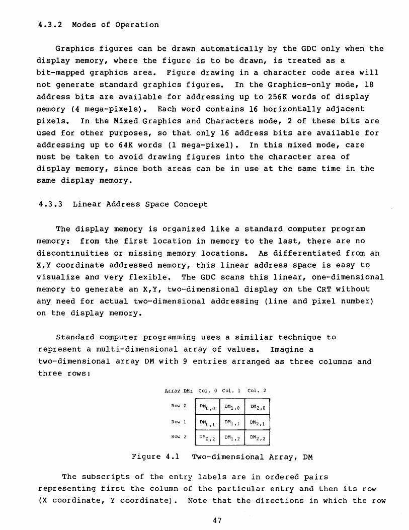
4.3.2 Modes of Operation
Graphics figures can be drawn automatically by the GDC only when the display memory, where the figure is to be drawn, is treated as a bit-mapped graphics area. Figure drawing in a character code area will
not generate standard graphics figures. In the Graphics-only mode, 18
address bits are available for addressing up to 256K words of display
memory (4 mega-pixels). Each word contains 16 horizontally adjacent pixels. In the Mixed Graphics and Characters mode, 2 of these bits are used for other purposes, so that only 16 address bits are available for addressing up to 64K words (1 mega-pixel). In this mixed mode, care must be taken to avoid drawing figures into the character area of display memory, since both areas can be in use at the same time in the same display memory.
4.3.3 Linear Address Space Concept
The display memory is organized like a standard computer program
memory: from the first location in memory to the last, there are no
discontinuities or missing memory locations. As differentiated from an X,Y coordinate addressed memory, this linear address space is easy to visualize and very flexible. The GDC scans this linear, one-dimensional memory to generate an X,Y, two-dimensional display on the CRT without any need for actual two-dimensional addressing (line and pixel number) on the display memory.
Standard computer programming uses a sirniliar technique to represent a multi-dimensional array of values. Imagine a
two-dimensional array DM with 9 entries arranged as three columns and three rows:
lll...J...gy OM.... Col. 0 Col. 1 Col. 2
Row a OMa,a OM1 ,0 OM2,O
Row 1 OMa ,1 OM1,1 OM 2 ,1
Row 2 OMa ,2 OM1 ,2 OM 2 ,2
Figure 4.1 Two-dimensirinal Array, DM
The subscripts of the entry labels are in ordered pairs representing first the column of the particular entry and then its row (X coordinate, Y coordinate). Note that the directions in which the row
47
and column numbers increase put the origin, (~~), in the upper left corner. This is similar to the fourth quadrant of the Cartesian plane:
y
II
III
Figure 4.2 Cartesian Plane
This array can be stored in a conventional linear memory only if its rows (or columns) are laid end to end in memory:
M0mory Address
1 2 3 4 5 6 7 8
\~ ____ ~¥ ____ -J~ \~ ____ ~¥ ____ -JI \~ ____ ~¥ ____ ~~
Top, R~l f4 Middle, Row 1 Bottom, Row 2
Figure 4.3 Conventional Linear Memory
This technique has a major advantage. To change to an array of a different size or dimension, no change to the memory structure is needed as long as the memory is large enough to hold all of the array entries.
Going back to the original array, we can enter the actual memory addresses in place of the ordered pairs:
S 1 2
3 4 5
G 7 8
I"'~---- p --............ 1 Figure 4.4 Array. OM
,Since this array is stored by rows, the number of entries in the array along that dimension (P or Pitch) is of fundamental importance. Any horizontal moves are accomplished with simple increments and decrements. Vertical moves require the addition or subtraction of P, while diagonal moves require a combination of both of these operations.
48
The GDC stores the two-dimensional array, the image to be displayed on the CRT, in its linear display memory in a fashion similar to our array example.
By choosing the quadrant of the numbering scheme to coincide with the raster-scanning process of the CRT, and using row (line) end to end storage, linear display memory is easily scanned to generate a video raster on the CRT.
4.4 Display Memory Contents
Because the GDC addresses the display through a l6-bit data bus, each word is interpreted differently depending on whether it is defined as a graphics or character area. In the Graphics mode, the 16 bits are used for 16 horizontally adjacent picture elements (pixels) which are serially output to the CRT. In the Character mode, some of the 16 bits
are sent through a character generator, where they are converted into the separate lines of pixels that make up the various characters. They
are then scanned out by repeatedly scanning the same row of display memory words while adding the lines. This line count is fed to the character generator to select which line of the character is to be displayed. Bits not sent through the character generator may be used to select various attributes that may affect the appearance of the displayed character. Typical attributes include blinking, underline, halt intensity, color, etc. These attributes are decoded externally to the GDC so that they are under the user's control.
For graphics display areas, the GDC assumes that the 16 bits of
each word are serially output to the CRT display in a particular order. The least significant bit, ~, is to be sent out first. The figure drawing algorithm uses this premise.
Sent to the CRT Dib~l~j usins a "rigilt shire."
EJ Figure 4.5 Word in Display Memory
Pr ev i (Jus Ne;; t: word word
Direction of :ilOti011 of tLcCWi' bear.1 spot.
Figure 4.6 Word Appearance on CRT
49
Note that the bit number increases toward the right, in the direction of increasing word address.
4.5 Specifying a Pixel Address in Display Memory
4.5.1 EAD and dAD Definitions
There can be up to 222 (4M where M = 1,048,576 = 220) pixels in the
display memory, organized into 218 (256K) l6-bit words. The address of
one of these pixels is specified to the GDC in two parts. First, an l8-bit address selects the display memory word which contains the pixel. Second, a 4-bit value pOints to the individual pixel within the word. The word address is called the Execute Address, or EAD, and effectively acts like a cursor in the GDC. The pixel address is called the dAD, or Dot Address.
4.5.2 X-y to Memory Address Conversion
Since it is likely that many GDC applications will maintain the vector list using X, Y representation, an example of the conversion from these X, Y coordinates to the linear display memory address is included. For simplicity, the origin (~,~) of our display will be in the upper left corner. This is the same point as the start of the CRT raster-scan. The commonly used origin position at the bottom left of the screen can be used with only a simple sUbstitution in the equations
we will develop. To get a clear idea of the conversion from X, Y address to linear address, letls define some terms:
4.5.2.1 Definitions
(.0,YMAX) XMAX, YMAX
Figure 4.7 Display Memory Shown as if Displayed
Where: (XMAX+l) is a multiple of 16 pixels up to 4096 (YMAX+l) is any number (up to a total of 4 mega-pixels on
display memory)
50
The actual displayed image can be no larger than the display memory structure ana must have an even multiple of 16 pixels in the horizontal direction, and no more than 1024 lines vertically (2048 interlaced display).
4.5.2.2 Upper Left Corner
Showing a close-up view of the upper left corner reveals the re1atlonship between dots and words as seen on the CRT display screen:
Word Address !6
* Word Address 1
Origin 16123456
16 1 2 3 456 7 8
·P"
Figure 4.8 Addresses of Dots within Their Respective Words
4.5.2.3 Word Addresses on Display Memory
A more global viewpoint shows the arrangement of word addresses:
1st word of 16 Pixels
• If P
2P
3P
4P
2nd 3 rd word word
W ,
1 2
P+l p+2
I
I I I I I
- - - - _,_'~ - - - - -" ,. L,
L~
LL
word Addresses in o i sp1 ay Memory
V· P-l
2P-l
3P-l
4P-1
5P-l
• Words /Line
~ ~
,~
1 st Line
2nd Line
3 rd Line
etc.
(n-l) F (n-l)P+l ('1-1)P+2- - - - - -;7 - - - - - - - - nP-l ",,,t Line #n ~L'
') !;~sC' Address uf ';a",j. Lille:
Figure 4.9 Word Addresses on Display Memory
Where: P = Number of 16 bit words across one line P = (XMAX + 1)/16
51
4.5.2.4 Finding the Word Addresses Given the X,Y Coordinates
Note the direction of increasing x and y values:
Origin (0,0)
Increasing
Increasing X
y .(x, y)
Figure 4.10 Direction of Increasing X,Y Values.
Beginning with the Y coordinate, y, at the point for which we need to find the absolute memory address, we can find the base address start1ng at the line in which the pixel lies:
Line Base Address = P * Y = LRA
To this we must add the number of words along the line due to the value of the X coordinate to find the actual EAD value:
EAD = LBA + INTEGER (X/16) = Py + INTEGER (X/16)
where the Integer Operation yields the integer part of the X/16 division, truncating off the fractional part or remainder of the division.
4.5.2.5 Finding the DOT Addresses
To find the dot addresses within the word determined in the EAD equation, take the residue or remainder of the division performed above and treat it as the integer value of the dot address:
dAD = REMAINDER (X/16) * 16
= RESIDUE (X/16)
Here's an example using actual values. Let the display memory be configured as 512 pixels by 512 lines (XMAX = YMAX = 511), and the pOint will be (X,Y) = (231,475) (All numbers use base 10 notation):
52
P = (XMAX + l}/16 = 512/1"6 = 32 Words/Line EAD = Py + INTEGER (X/16)
= 32(475) + INTEGER (231/16 ) = 15, 200 + INTEGER (14.43750)
= 15,214
dAD = RESIDUE (X/16) = RESIDUE (14.43750) = 16 x 0.4375 = 7
These two numbers, (converted to base 2) can be sent to the GDC to specify the particular pixel of interest.
4.5.2.6 Calculation Considerations
Note that all the values are unsigned positive integers. Certainly,
this is the easiest format with which to work. In addition, with the possible except10n of the multiplication by Up" in the dAD calculation, all the multiplication and division is accomplished by simple shifts and
done by powers of two. If the display memory is a "power of two" pixels
wide, the "p" will be also. Its multiplication will be just arithmetic shifts. If memory is structured with other than a "power of two" width,
a real multiply instruction will be needed. If the processor doing these calculations does not have a multiply instruction, the I·shift and
add" multiply routine is neither difficult nor time-consuming to write.
4.5.2.7 Other Coordinate Systems
Setting the origin at another point on the screen does not seriously complicate the physical memory address calculation. Imagine a system witn a lower left corner origin, denoted by primed coordinates:
(.0, YMAX) (XMAX, YMAX)
(x,y)
(~,/8) (XMAX,g)
Figure 4.11 Origin at Lower Left
53
A simple coordinate translation relationship can be defined between these two systems:
x = Xl
Y = YMAX - yl
With these expressions substituted into the EAD and dAD equations, only one difference is noted:
EAD = P (YMAX-yl) + INTEGER (Xl /16)
dAD = RESIDUE (Xl /16)
Any other coordinate system can be similarly defined.
4.5.2.8 Display Memory Organization
Let's examine the display memory organization before explaining how to calculate the parameters for figure drawing.
The GDC in the Graphic Display mode provides 18 address lines, 16 lines of these also serving as a bi-directional data bus. This interface to the display memory allows direct control of all 262,144 or 25bK (where K = 1024) addresses, each containing 16 bits of data for a total of 4096K bits of memory.
If each bit of display memory corresponds to one pixel on the display screen (for a black and white monitor), this allows the system
to be configured in several ways: for example, 2048 x 2048, 4096 x 1024, or any other combination. Since today's CRT monitor technology does not generally allow resolutions this high without prohibitively high costs, in most applications the display area will be of a smaller size, such as 512 x 512, 768 x 576, etc. In this instance, the display memory contains many pages of the display area or it can be used for displaying a smaller window of a much larger image.
Design of a color graphics system needs special consideration. The
most common way of implementing color is by building multiple planes of
the display memory, each plane representing one of the primary colors. By senaing the video data from all the planes together, a large number of colors may be generated. For example, with three planes (red, blue
54
and green) a total of six colors, plus black and white, may be generated. A similar technique can be used for generating monochrome grayscale displays.
4.6 Drawing Directions
Every figure drawn by the GDC consists of a large number of individual bits that must be modified in the display memory. As figure drawing proceeds, the next pixel to be modified can be anyone of the eight nearest neighbors of the current figure pixel. The figure drawing hardware decides which direction to proceed based on the selected drawing algorithm and position within the figure. DIR 0 lies in the direction of the pixel directly below (as it would be seen on the display screen), and the direction number assignments then proceed in a counter-clock-wise fashion through all eight directions.
Figure 4.12 Drawing Directions
Determining the next pixel of the figure during figure drawing
requires the proper manipulation of the word address and the pixel bit position according to the drawing direction. To move to the pixel below or above, it is necessary to add or subtract the number of memory words
per l1ne to or from the word address pOinter, EAD. This offset is the "pitch", P, of the display memory. To move to a pixel to the right or left across a word boundary, the EAD is incremented or decremented and the MASK register is shifted in the proper direction with end wrap-around. For diagnol directions, the add/subtract of P operation must be combined with MASK register shifting. Table 1 summarizes these operations for each direction.
55
Dir Operations to Address the Next Pixel
000 EAD + P-EAD
001 EAD + P-EAD dAD (MSB) = 1 :EAD + 1 - EAD
010 dAD (MSB) = 1:EAD + 1-EAD
011 EAD - P-EAD dAD (MSB) = 1 :EAD + 1 - EAD
100 EAD - P--EAD
101 EAD - P ..... EAD dAD (LSB) = 1:EAD -1 ..... EAD
110 dAD (LSB) = 1 :EAD - 1-EAD
111 EAD + P ..... EAD dAD (LSB) = 1 :EAD - 1-EAD
Where P = Pitch, LR = Left Rotate, RR = Right Rotate, EAo = Execute Word Address, and dAD = Dot Address stored in the Mask Register.
dAD ..... LR
dAD ..... LR
dAD-LR
dAD ..... RR
dAD--RR
dAD--RR
Table 4.1 Operations to Address the Next Pixel
When a figure is being specified to the GDC for figure drawing, the initial dir~ction, DIR, must be supplied. The various figures are thereby given their basic rotational orientation. As drawing progresses, the drawing direction is adjusted by the GDC for each pixel,
where necessary, so that pixels in the right positions are modified to draw the figure.
4.7. Initial Drawing Direction
For the various figures, the effect of the initial direction specification upon the resulting drawing is shown in Table 4.2. For each of the eight initially specified directions, the various figure orientations are shown. The heavy dot in each of the drawings in the table represents the starting point of the figure drawing process.
OlR LINE ARC CHARACTER SLANT CHAR. RECTANGLE oMA
000 rN
~ 010 z= 011" C:~~ ~ ~ 0 ~ 100 ,.,~ .(::J f\J1J1J1 , D l'N
~ 110" ~ ~ ff 0 ~ - - -
- - . 111 A '~~,-) ~ ~ 0 ~
Table 4.2 Figure Orientations
56
For lines and vectors, Table 4.2 shows the range of line directions which can be handled within each initially specified direction octant. Note that a line to be drawn along the counter-clockwise boundary of each octant should be drawn using the next higher DIR value.
For drawing arcs, the starting point in each octant is on its
coordinate axis. The arc is then drawn toward the octant's diagonal boundary. The tangential arrow in Table 4.2 shows the initially specified direction. The iterative nature of the digital differential analyzer's operation requires that it calculate all the pixel addresses from a starting point on the axis to the end of the arc. Any pixels between the start of the arc and the axis are calculated but not drawn into the display memory. The specifications for these arbitrary arc lengths are computed by the host computer using two angles measured from the octant's coordinate axis. The angle measured to the far end of the arc is used to compute the total number of pixels. The angle to the start of the arc yields the number of pixels not to be included in the figure. Both of these numbers are given to the GDC as parameters in the FIGS command. Arcs which cross the boundaries of octants must be broken down into arc segments, each constrained to one octant. Circles are drawn using eight full 45 degree arcs.
3 4
180 0 0°
0 7
225 0 5 2 315 0
270 0
Figure 4.13 Arc Drawing Directions
57
(r, ~)
Figure 4.14. Arc Drawing within an Octant
Figure 4.15. Arc Drawing Across Octant Boundaries
For vectors and arcs, the slope and radius of curvature information
within the octant is specified by other parameters of the Figure Specify commana, FIGS, as will be discussed below.
TO draw graphics characters, the contents of the GDC's Parameter RAM is moved into the bit-map display memory one pixel at a time. The
Parameter RAM is scanned in the same order for any of the drawing directions so that the drawn characters appear merely to be rotated
arouna the starting point. Although the Parameter RAM holds 64 bits in an eight-by-eight array, the pattern drawn can be made smaller or larger than this by supplying the appropriate FIGS parameters. If larger, the pattern drawn into display memory is a repetition of the pattern in the Parameter RAM in both the x and y directions. This ~rawing mode can be used to fill an area in the display memory with solid or pattern, in addition to drawing bit-mapped characters.
Slanted graphics characters and area filling patterns are drawn in a
fashion similar to graphics characters, except that each row of pixels in ~e character is offset by one pixel position sideways from the previous row. The result is a 45 degree slanting effect similar to ita11cs printing. Slanted graphics characters can also be drawn in all of the octant directions, in each case maintaining the slanted appearance.
58
For rectangle drawing, the GDC is given the pixel counts for the two adjacent sides of the rectangle and one of eight initial directions. As
with graphics characters, 45 degree rotated rectangles are generated with odd DIR values. The sides of the rectangle can be up to 16K pixels long per side.
DMA transfers are handled on a word basis instead of a pixel basis. In this way, very high-speed transfers can be made to and from solid rectangular areas of display memory. Table 4.2 shows the starting word address in display memory with a heavy dot for each of the drawing directions. The next word to be accessed is found in the direction of the arrow. The specified number of words is transferred using the
initially specified direction, and then the next group is accessed, repeating until the specified number of groups is transferred. The 45 degree rotated patterns advance the word address both vertically and
horizontally as the arrow paths are followed.
4.8 The Digital Differential Analyzer
The Digital Differential Analyzer, DDA, in the GDC generates figures from their differential equations with dedicated hardware at very high speed. The DDA works in parallel with the Read-Modify-Write (RMW) hardware to form a pipelined system for figure drawing. Both lines and
circles can be drawn, as well as derived forms such as rectangles, graphics characters, and DMA transfers. The figures are drawn into display memory using back-to-back RMW drawing cycles while the DDA is calculating the address of the next pixel of the figure.
The analyzer used in the GDC uses one coordinate axis direction (eitner the x or y axis) as the independent axis of the figure in that octant. The pixel count along this direction is equal to the total number of pixels in that figure segment, because the analyzer advances
along this axis for each pixel that is drawn. The other axis direction
is the dependent axis, and the pixel distance in this direction is
always less than or equal to the distance along the independent axis. As each pixel is drawn, the dependent axis mayor may not be advanced, depending on the figure type and the position within th€ figure. The result is that the figure's pixels are always within one half-pixel of
the mathematically ideal position of the figure. The independent axis advance can occur in the +x, -x, +y, or -y direction, depending on the DIR specified octant. The host computer must determine the appropriate
59
parameters for the desired figure in these terms and use the DIR parameter to provide the correlation to the actual figure's orientation.
4.9 The Figure Drawing Process
Once all the commands and parameters have been interpreted by the
GDC's command processor and the drawing process begins, the Digital
Differential Analyzer and the RMW hardware work together to do the figure drawing (or DMA transfers, etc). They are designed to work in parallel with each other, so that while the RMW logic is modifying a pixel in the figure, the DDA is determining the address of the next pixel. Thus, drawing proceeds at the fastest rate possible for this hardware.
There are two levels in this pipeline: the DDA and the RMW logic.
If no cycles are to be wasted, the first pixel address must be supplied by a source outside the DDA so that the RMW logic can have something to
modify during the first cycle. Of course, this is no problem, since the host microprocessor must supply the address of the first pixel anyway (cursor position). It is important to note that the dot count (really an address calculation cycle count) provided to the DDA does not include this first cycle which draws the first pixel. Also interesting to note is that when the dot count expires and while the last pixel is being
written into display memory, the DDA calculates the address of the pixel which would have been drawn next if the dot count had been greater and
leaves the cursor values, EAD and dAD, pointing at this pixel.
4.10 Preparing the GDC for Figure Drawing
To prepare the GDC to draw a figure, the details of the desired drawing operation must be loaded into the GDC through the command and
parameter FIFO. The type of RMW cycle modification can be selected using the WDAT command followed by no parameters. The cursor can be
positioned using the CURS command to the word and dot address, EAD and dAD, of the starting pixel of the figure. Parame~er RAM bytes 8 and 9 mus~ be loaded with the drawing pattern for continuous, dotted, dashed, etc. figure lines using the PRAM command. For graphics character drawing and patterned area filling, Parameter RAM bytes 8 through 15 can
be loaded with the desired pattern or character. In either case, the Figure Specify command, FIGS, is used to set up the Digital Differential
60
Analyzer, DDA, for the desired fi"gure, and a figure drawing command, FIGD or GCHRD, is issued to begin the actual drawing process.
During the read-modify-write memory cycles needed to draw the desired figure into display memory, the type of logical operation
pertormed can be selected from among the following: SET, CLEAR,
COMPLEMENT, and REPLACE. The WDAT command can be used to configure the
GDC for the desired operation. The TYPE field (command byte bits 3 and 4) should select word transfers (00 code), and command bits 0 and 1,
then select the logical operation.
BIT: 7 6 5 4 3 2 1 0
0 0 1 TYPE-l TYPE-O 0 MOD-l MOD-O
Table 4.3 The WDAT Command Format
Bits 1 and 0 Operation
0 0 REPLACE the addressed pixel bit with the value
in the Pattern register's selected bit position.
0 1 COMPLEMENT the addressed pixel bit if the
selected bit in the Pattern register is a ONE.
1 0 RESET the addressed pixel bit to a ZERO if the
selected bit in the Pattern register is a ONE.
1 1 SET the addressed pixel bit to a ONE if the
selected bit in the Pattern register is a ONE.
Table 4.4 RMW Logical Operations
The WDAT command byte must not be followed by any parameter bytes when only used to set the RMW modification operation. If parameters were to follow, the GDC would move them into display memory as it would if a block data transfer were intended. The next command byte will terminate the WDAT command-byte-only sequence without any parameters.
Parameter RAM bytes 8 and 9 must contain the pattern to be drawn as
the figure. As figure drawing begins, the contents of these RAM bytes will be moved into the Pattern register and used by the RMW hardware to enable or disable the modification of the individual pixel bits of the figure as their addresses are calculated during drawing. In Graphics mode, the Pattern register bits are used one at a time as selected by a
counter which increments after each RMW cycle. The LSB of the pattern is the first bit to be used for the patterning. The second RMW cycle uses the second bit, etc. The pattern impressed on the figure is
61
repeated every 16 RMW cycles. Because any 16-bit pattern can be put in
the Parameter RAM before drawing, any modulo-16 pattern may be generated along the figure. The Pattern register is always scanned in the same
sequence, regardless of the type or direction of the figure being drawn.
4.11 FIGS Parameters for Figure Drawing
The Figure Specify, FIGS, command's parameters control the figure to be drawn. Its first parameter byte configures the DDA for the basic figure type. The rest of the parameter bytes load the different variables to guide the DDA during figure drawing. Each variable is a 14-bit integer which is loaded by the GDC's command processor into the appropriate register using two parameter bytes. Where the parameters
can be either positive or negative, 2's complement notation should be used. This is an easy requirement to meet when using a microprocessor or minicomputer to drive the GDC, as these machines commonly use 2's complement arithmetic internally. The interpretation of these values by the DDA varies with different figure types.
The five figure drawing variables are called DC, D, D2, Dl, and DM, and their interpretation by the DDA varies for the various figure types. They are accepted by the GDC in this order only.
As the GDC's command processor executes each FIGS command opcode,
the various DDA registers have specific initial values: DC = 0,
D = 8, D2 = 8, Dl = -1, and DM = -1. To change these values the appropriate parameter bytes must follow the FIGS command byte. In several figure types, some of these initial values need not be changed and consequently those parameter bytes need not be sent to the GDC. The internal command processor in the GDC accepts the parameters as they come ana puts them in the appropriate DDA registers in a fixed sequence.
This,loading process is terminated by any command byte, such as the Figure Drawing Start command, FIGD. Therefore, it is possible to load only the first two variables, or the first three, etc. It is NOT
possible to load the first, skip the second and load the third variable, for example.
The first parameter byte describes the type of figure to be drawn. The top five bits are set to indicate the various figure types. Just
62
one of these bits can be set at a time, except for the Slant bit, which can be used in conjunction solely with the Area Filling bit. Use the specific bit combinations listed below exclusively, as only these assure
correct drawing operation.
Figure Drawing Parameters Specify
FIGS: I 0 ! 1 0 0 o 0 I P1
Table 4.5
Drawing Direction Base
Figure Type Select Bits: '------- Line (Vector)
'---------- Graphics Character --- Arc/Circle
---------Rectangle Slanted Graphics Character
FIGS Parameter Byte 1
Valid Figure Type Select Combinations
__________________________ O~p_e_ra~ti~on ~----Character Di~ay Mode Drawing~.tnaividual Dot Drawing, DMA, WDAT,.and RDAT
SL R A GC L
0 0 0 0
0 0 0 0
0 0
0 0
0 0
0 0
0
0
0
0
0
Straight Line Drawing
Graphics Character Drawing and Area filling with graphics character pattern
Arc and Circle Drawing
Rectangle Drawing
Slanted Graphics Character Drawing and Slanted Area Filling
Table 4.6 Figure Type Select Bit Combinations
The DIR bits specify the initial drawing direction to the DDA to
control the orientation of the resulting figure. Typically the Figure Type Select bits are known before any figure drawing parameters are
calculated for each figure, as the first step in determining the other DDA parameters.
4.12. FIGS Command Type Parameter
4.12.1 Introduction
The Figure Specify GDC command, FIGS, sets up the GDC's Digital Differential Analyzer (DDA) to perform one of a number of
read-modify-write (RMW) operations. The DDA can generate six different types of operations in any of eight octants, with wide parametric variations. After the FIGS command has prepared the DDA to do the
63
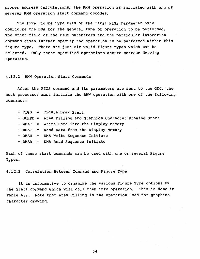
proper address calculations, the RMW operation is initiated with one of several RMW operation start command opcodes.
The five Figure Type bits of the first FIGS parameter byte configure the DDA for the general type of operation to be performed. The other field of the FIGS parameters and the particular invocation commana given further specify the operation to be performed within this figure type. There are just six valid figure types which can be selected. Only these specified operations assure correct drawing operation.
4.12.2 RMW Operation start Commands
After the FIGS command and its parameters are sent to the GDC, the host processor must initiate the RMW operation with one of the following commanas:
- FIGD = Figure Draw Start - GCHRD = Area Filling and Graphics Character Drawing Start
- WDAT = Write Data into the Display Memory
- RDAT = Read Data from the Display Memory
- DMAW = DMA Write Sequence Initiate
- DMAR = DMA Read Sequence Initiate
Each of these start commands can be used with one or several Figure Types.
4.12.3 Correlation Between Command and Figure Type
It is informative to organize the various Figure Type options by the Start command which will call them into operation. This is done in Table 4.7. Note that Area Filling is the operation used for graphics
character drawing.
64
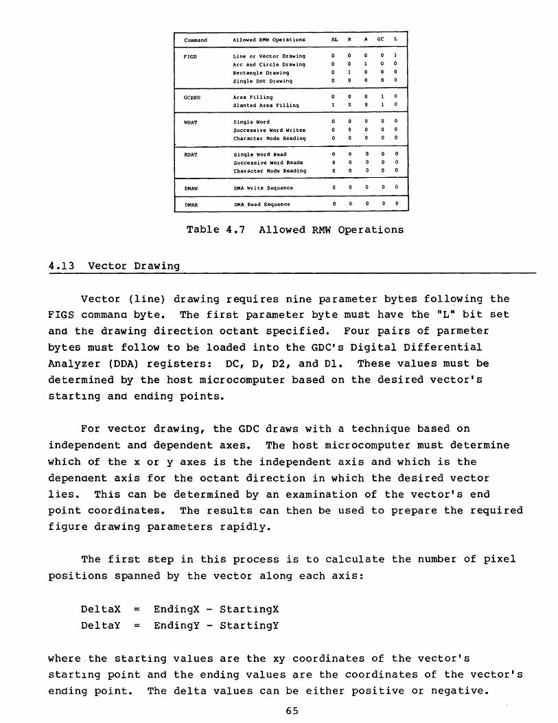
Command Allowed RMW Operations SL R A GC L
FlGD Line or Vector Drawing 0 0 0 0 1
Arc and Circle Drawing 0 0 1 0 0
Rectangle Drawing 0 1 0 0 0
Single Dot Drawing 0 0 0 0 0
GCHRD Area Filling 0 0 0 1 0
Slanted Area Filling 1 0 0 1 0
WDAT Single Word 0 0 0 0 0
Successive Word Writes 0 0 0 0 0
Character Mode Reading 0 0 0 0 0
ROAT Single word Read 0 0 0 0 0
Successive Word Reads 0 0 0 0 0
Character Mode Reading 0 0 0 0 0
DMAW DMA Write Sequence 0 0 0 0 0
DMAR OMA Read Sequence 0 0 0 0 0
Table 4.7 Allowed RMW Operations
4.13 Vector Drawing
Vector (line) drawing requires nine parameter bytes foll~wing the FIGS commana byte. The first parameter byte must have the "L" bit set
and the drawing direction octant specified. Four pairs of parmeter
bytes must follow to be loaded into the GDC's Digital Differential Analyzer (DDA) registers: DC, D, D2, and 01. These values must be determined by the host microcomputer based on the desired vector's start1ng and ending points.
For vector drawing, the GDC draws with a technique based on
independent and dependent axes. The host microcomputer must determine
which of the x or y axes is the independent axis and which is the depenaent axis for the octant direction in which the desired vector lies. This can be determined by an examination of the vector's end pOint coordinates. The results can then be used to prepare the required figure drawing parameters rapidly.
The first step in this process is to calculate the number of pixel
positions spanned by the vector along each axis:
DeltaX = EndingX - StartingX DeltaY = EndingY - StartingY
where the starting values are the xy coordinates of the vector's start1ng point and the ending values are the coordinates of the vector's ending point. The delta values can be either positive or negative.
65
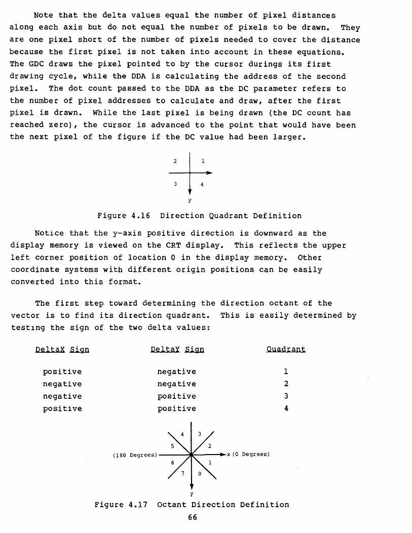
Note that the delta values equal the number of pixel distances along each axis but do not equal the number of pixels to be drawn. They
are one pixel short of the number of pixels needed to cover the distance
because the first pixel is not taken into account in these equations. The GDC draws the pixel pointed to by the cursor durings its first drawing cycle, while the DDA is calculating the address of the second pixel. The dot count passed to the DDA as the DC parameter refers to
the number of pixel addresses to calculate and draw, after the first pixel is drawn. While the last pixel is being drawn (the DC count has reached zero), the cursor is advanced to the pOint that would have been the next pixel of the figure if the DC value had been larger.
2 1
3 4
y
Figure 4.16 Direction Quadrant Definition
Notice that the y-axis positive direction is downward as the display memory is viewed on the CRT display. This reflects the upper left corner position of location 0 in the display memory_ Other coordinate systems with different origin positions can be easily converted into this format.
The first step toward determining the direction octant of the vector is to find its direction quadrant. This is easily determined by testlng the sign of the two delta values:
DeltaX Sign
positive
negative
negative positive
DeltaY Sign Quadrant
negative 1
negative 2
positive 3
positive 4
(180 Degrees) x (0 Degrees)
y
Figure 4.17 Octant Direction Definition
66
Within the quadrant, the direction octant may be determined by comparing the absolute value magnitudes of the two delta values:
If ABS (DeltaX) is greater than ABS (DeltaY) ,
and the quadrant is: then the octant is:
1 2
2 5
3 6
4 1
If ABS (DeltaX) is smaller than ABS (DeltaY),
and the quadrant is: then the octant is:
1 3
2 4
3 7
4 0
If ABS (DeltaX) = ABS (DeltaY), the vector is on the diagonal octant boundary within the quadrant. The higher numbered, odd octant of the quadrant can be chosen in this case to maintain symmetry with vector direction assignments along the coordinate axes.
These tests can be made at high speed if the signs of the two delta terms and their difference are used to index into a software table.
With the vector's direction determined to be within a particular octant, the next step is the determination of the independent drawing axis and calculation of the drawing parameters. The independent axis will be the x-axis for those octants where ABS (DeltaX) > ABS (DeltaY), and it will be the y-axis for those octants where ABS (DeltaX) , ABS
(DeltaY), where "'" means "less than or equal to". As can be seen from the octant direction drawing, the y-axis is the independent axis for those octants where the line is longer in the y direction than it is in the x direction.
67
Octant Independent Axes:
Octant Independent Ax.ia Dependent Ax.ia
0 y x 1 x Y 2 x Y 3 Y x 4 Y x 5 x Y 6 x Y 7 y x
The GDC' s DDA drawing parameter"s can be calculated from the
absolute values of DeltaX and DeltaY. The octant drawing direction parameter, DIR, directs the DDA to advance along the independent axis by
incrementing or decrementing the x-address or the y-address, depending on which octant direction is specified. Similarly, the manipulation
required to advance along the dependent axis is also implicitly specified by the DIR parameter.
Line Drawing Parameter Equations: (I=Independent Axis, D=Dependent
Axis)
DC = ABS (DeltaI).
D = 2 * ABS (DeltaD) ] - ABS (DeltaI).
D2 = 2 * [ ABS (DeltaD) - ABS (Delta!) ].
Dl = 2 * ABS (DeltaD).
It will be necessary to sUbstitute the appropriate Deltax and DeltaY values for the Delta! and DeltaD terms in these equations as required by the drawing direction octant. The calculations of D and D2 require l6-bit integer, 2 1 s complement arithmetic. The values sent to the GDC should include only the low 14 bits. Both the DC and Dl values will be unsigned integers with a range of 0 to (2**14) - 1. Note that
the DC parameter contains the pixel (dot) count for the figure minus
68
one, since the count does not include the first pixel. The other three parameters encode the slope of the line as values to be used by the DDA to determine when to advance along the dependent axis as vector drawing proceeds.
4.14 Vector Drawing Example
An example of calculating a vector's figure drawing parameters will help make clear the procedure outlined above. Note that all numbers will be shown as sign/magnitude decimal numbers, when in reality they must be given to the GDC in 2's complement or unsigned integer binary form. The starting address is given to the GDC as an unsigned integer
via the CURS command, and it must use the linear addressing technique of the Display Memory. The example's starting and ending points, expressed as (x, y) ordered pairs, will be:
starting Point = (100,100) Ending Point = (78,34)
As seen on the CRT display screen, this vector would appear like this:
78 100 0, a -+------i-------II--I~ x
34
100 (100,100)
y
Figure 4.18 Vector Drawing Example
To determine the direction of the vector, the first step is to calculate the DeltaX and DeltaY values:
DeltaX = EndingX - StartingX = 78 - 100 = -22
DeltaY = EndingY - StartingY = 34 - 100 = -66
69
Both of these values are negative; therefore the vector lies in the secona quadrant.
To determine the direction octant within the quadrant, we notice
that the absolute value of DeltaY is larger than the absolute value of
DeltaX, which corresponds to a vector direction in Octant 4, so that:
DIR = 4
In Octant 4, the independent axis is Y and the dependent axis is x. Therefore we can define:
DeltaI = DeltaY = -66
DeltaD = DeltaX = -22
The line drawing parameters for the FIGS command can be easily calculated as follows:
DC = ABS (DeltaI) = 66
D = [ 2 * ABS (DeltaD) ] - ABS (DeltaI)
= [2 * 22] - 66 = -22
D2 = 2 * [ ABS (DeltaD) - ABS (DeltaI) ]
= 2 * [22-661 = -88
Dl = 2 * ABS (DeltaD) = 2 * 22 = 44
When expressed in the appropriate binary notation and loaded into
the GDC, along with the other setup commands and parameters, the GDC will draw the desired vector using 67 RMW Display Memory cycles. Both
DC and Dl will always be unsigned integers for vector drawing. They
have the full 14-bit range of values from 0 to 16, 384 - 1. D and D2,
on the othr hand, must use 2's complement notation for a range of values
fro~ 8192-1 to -8192.
4.15 Vector Drawing Algorithm
Let's consider some arbitrary vectors to understand better the
parameters that the GDC needs during vector drawing.
70
The equation of the straight line may be expressed as follows:
Y2 = dx (X2 - Xl) - Yl dy
where Xl, X2, Yl, and Y2 are coordinates of the starting and ending point of the vector. If we normalize the vector so that the starting point is at (0,0) coordinates, the equation takes this form:
Y = ADY • X ADX
where X and Yare coordinates of each consecutive pixel of the vector.
Since in the raster drawing system X and Y values can only be positive
integers, it could be expressed as follows:
Y = ADY * X = ADX
I + F
Where X is consecutive X coordinates (1,2,3 ••• ),
I is the integer part of Y coordinates (0,1,2 ••• ), or
F is a fractional part of Y coordinates (0 < F < 1).
The F value of this equation must be rounded off to the nearest integer. In the case where F = 0.5, the I value is incremented by 1 or rounaed up. To decide when to round up or round down, the F value must be evaluated by GDC logic at each pixel address. Equation 2 takes the following form to isolate the fractional part:
F = ADX • X-I ADY
Rounding up takes place when:
or
F > 0.5
ADX • X - I > 0.5 ADY
71
The equation achieved by multiplying both sides by two and subtracting 1 is:
ADY • X - 2I - 1 > 0 2-ADX
The equation achieved by multiplying it byADX is:
2ADY • X - (2I + I) ADX > 0
The hardware in the GDC uses this equation in calculating each
consecut~ve pixel address. Since it does the calculation of only the next pixel to be drawn at any given moment, the equation could be further simplified.
The first pixel of the vector is drawn at the point specified as a starting point of the vector by the CURS command. At this point X = 0
ana I = o.
For the second pixel, the X value is incremented and I is still equal to zero. That is because the ADX > ADY; therefore the Y value will be incremented only if F > 0.5. To evaluate the value of F, equation (1) must be evaluated.
D = 2ADY • X - (2I + 1) ADX, and
for X = 1 and I = 0, D = 2ADY - ADX
Based on the sign of the value D, the next value of the Y coordinate (I) is rounded up or down. If D > 0, I is incremented by one. If D < 0, I is not modified. Depending on the sign of the parameter D, the next pixel could be drawn in one of two positions, either above or below the ideal line.
Situation~: ~ Jl ~ .a.
The only parameter between two consecutive pixels that is
incremented is the X value (increment is in X direction) and Equation 4 takas form:
Dl = (2ADY (X+l) - (21+1) ADX» -(2ADY.X-(2I+l) ADX) = 2ADY
Next Pixel Present Pixel
This value is added to value D for the next pixel if D was negative.
72
Situation 2: ~ D L ~
Both the X and I parameters are incremented and Equation 4 takes
form,
D2 = (2ADY (X+l)-(2(I+l)+1)*ADX)-(2.ADY.X-2(I+l)ADX) = 2(ADY-ADX)
Next Pixel Present Pixel
This is added to the value of D, if D was positive or zero.
The parameters D, Dl, and D2 must be supplied to the GDC before the
drawing process starts. The only other parameters that are necessary are the total number of pixels to be drawn, excluding the first pixel.
This number is always equal to ADX. The seven parameters that the CPU must provide to the GDC are:
1. EAD = Word address of the first pixel
2. dAD = Address of the pixel in the EAD of the first pixel
3. DIR = One of the eight directions
4. DC = ADX or Total number of pixels - 1 to be drawn
5. D = 2ADY - ADX
6. DL = 2ADY
7. D2 = 2(ADY -ADX)
The last three parameters must be loaded into the GDC using 2's
complement notation signed integers.
4.16 Arc and Circle Drawing
The GDC's Digital Differential Analyzer (DDA) can draw arcs
sUDtenaing up to 45 degrees on one octant. ~ircles can be drawn using
eight arcs, each having the same radius of curvature and center, and
each spanning 45 degrees of the total circle. Using the same principle of indepenaent and dependent axes that is used for vector drawing, arc
drawing is limited to one octant per invocation, so that the advance of
73
the x and y pixel addresses during drawing can always proceed in the same direction.
To draw an arc, the GDC is given a starting pixel address with a CURS commana, a pattern with a PRAM command load into bytes 8 and 9 (if the previous pattern was different or in doubt), an RMW logical
modification operation selection with a WDAT command (if the last
specification was different or in doubt), a FIGS command to set up the DDA for the arc, and a FIGD command to initiate the drawing process. The only difference between this and a vector writing command sequence is the parameters of the FIGS command.
4.17 Arc Drawing Cursor Positioning
The Cursor Specification command, CURS, is used to position the cursor to the point on the arc where it intercepts the X or Y axis in the particular octant in which the arc is to be drawn. The arc is
always drawn in a direction away from this axis and toward the diagonal octant boundary. When circles are drawn, although there are eight arcs
required to form the entire circle, there are, therefore, only four
startlng pOints, each of which is used for two of the arcs.
3 4
180 0 00
0 7
225 0 5 2 315 0
270 0
Figure 4.19 Arc Drawing Directions Around a Circle
Notice in the above diagram that there are four initial directions which can each bend either counter-clockwise or clockwise, depending on the DIR value specified. The relationship of the various DIR values to drawing direction can be seen more clearly in Figure 4.20.
74
4 3
5 2
6 1
7 0
Figure 4.20 Arc Drawing Directions From a Point
Arcs which are to be drawn across octant boundaries must be drawn in arc segments which do not cross boundaries. If the dot count (DC)
given to the DDA in the FIGS command results in the drawing crossing the octant's diagonal boundary, the resulting figure will look like an arc
only up to the point where it crosses out of the initial octant. The last three parameters must be loaded into the GDC using 2's complement notation signed integers.
4.18 Calculating Arc FIGS Parameters
The initial values available to the GDC software driver for circle and arc drawing are often the center of the circle (or center of
curvature for an arc), the radius, and, for arcs, the initial and final angles subtended as measured from the center of curvature. Using a straightforward example in Quadrant 1, the specifications of an arc might be as shown below.
Figure 4.21 Arc Drawing Within an Octant
In Figure 4.21, the initial drawing direction, DIR, is four and the independent axis is Y. Note that a vector drawn by the GDC from the arc's center of curvature will use a DIR = 2 to be drawn in this area of the circle, while the arc uses a direction initially tangential to the
radius of the arc so that its initial DIR is at right angles to the
75
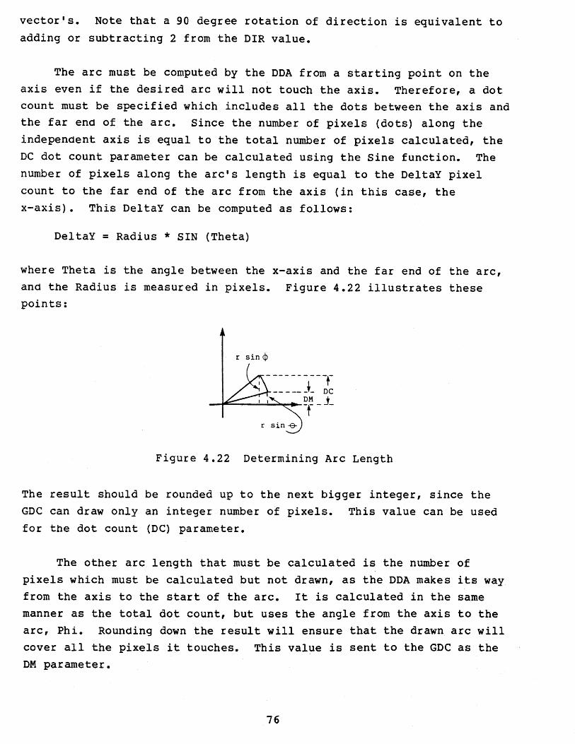
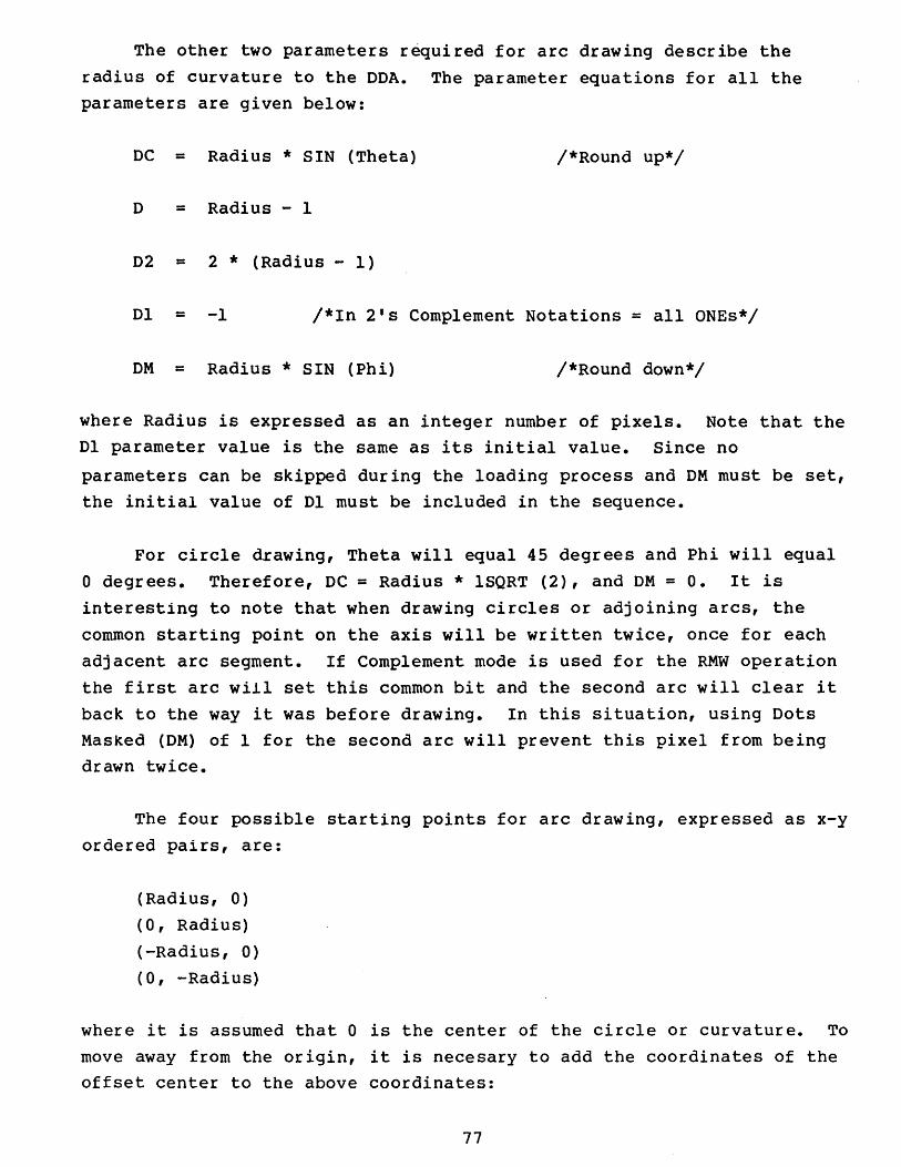
The other two parameters required for arc drawing describe the radius of curvature to the DDA. The parameter equations for all the parameters are given below:
DC = Radius * SIN (Theta) /*Round up*/
D = Radius - 1
D2 = 2 * (Radius - 1)
Dl = -1 /*In 2's Complement Notations = all ONEs*/
DM = Radius * SIN (Phi) /*Round down*/
where Radius is expressed as an integer number of pixels. Note that the Dl parameter value is the same as its initial value. Since no
parameters can be skipped during the loading process and DM must be set, the initial value of Dl must be included in the sequence.
For circle drawing, Theta will equal 45 degrees and Phi will equal o degrees. Therefore, DC = Radius * lSQRT (2), and DM = O. It is interesting to note that when drawing circles or adjoining arcs, the
common starting point on the axis will be written twice, once for each adjacent arc segment. If Complement mode is used for the RMW operation the first arc will set this common bit and the second arc will clear it back to the way it was before drawing. In this situation, using Dots Masked (DM) of 1 for the second arc will prevent this pixel from being drawn twice.
The four possible starting points for arc drawing, expressed as x-y ordered pairs, are:
(Radius, 0) (0, Radius)
(-Radius, 0) (0, -Radius)
where it is assumed that 0 is the center of the circle or curvature. To move away from the origin, it is necesary to add the coordinates of the offset center to the above coordinates:
77
(Radius + CenterX, CenterY)
(CenterX, Radius + CenterY)
(CenterX - Radius, CenterY)
(CenterX, CenterY - Radius)
where CenterX is the x-coordinate of the center, and CenterY is the
y-coordinate of the center.
4.19 Rectangle Drawing
The GDC can draw four line segments in the form of a rectangle with a single CURS, FIGS, and FIGD command sequence. (This assumes that the drawing pattern and RMW operation have previously been set.) starting
from the cursor position, the DDA draws four line segments, in series, with a counter-clockwise, 90 degree turn at each intersection. The initially specified direction may be anyone of the eight DIR values, so
that the figure drawing may start in any corner of rectangles which are either horizontal or 45 degree-rotated.
Rectangle drawing requires five parameters with the FIGS command. The only calculation to be made by the host microprocessor is the number of pixels to be drawn on each side of the rectangle. This is passed to
the GDC in the form of two values. The first value specifies the number
of pixels in the direction given by the DIR parameter, which will be
along the first side of the rectangle to be drawn. The second value specifies the length of the second side to be drawn, which will be at right angles to the first side. These two values can be thought of as the height and width of the rectangle. The exact values to be sent to the GDC as parameters to the FIGS command are:
DC = 3
D = (Number of Pixels in the Initially Specified Direction) - 1
D2 = (Number of Pixels in the Perpendicular Direction) - 1
'Dl = -1
DM = Same value as parameter D
78
A sample rectangle would be drawn like this:
Initial cursor---4~~***************************1 position * *
* * , * . *
Initial
OIR
* * 9 Pixels
* * l * * * * ***************************------
L 27 Pixels --.J Figure 4.23 Example of Rectangle Drawing
t
Asterisks indicate pixels modified during drawing, and the arrows show the successive drawing directions used during the drawing process for the parameters given below:
OIR = 0 OC = 3 D = 8
D2 = 26 Dl = -1 DM = 8
4.20 Area Filling and Graphics Character Drawing
The contents of Parameter RAM bytes 8 through 15 can be transferred
into display memory starting at any pixel position. When filled with the desired pattern or character, the Parameter RAM acts as a temporary holding buffer which, until over-written, can be moved into display memory as many times as desired, to any pixel position, and in any of the eight 45 degree rotation orientations selected by the DIR value. In addition, the pattern may be magnified at the time of writing by a zoom factor from 1 to 16. The enlargement is accomplished via pixel
replication in both the x and y directions.
79
This drawing capability fills all the pixels in a rectangular or slanted rectangular area based on the Parameter RAM contents. The RAM is scanned from the LSB of byte 15, toward its MSB, then up to the MSB of byte 14, toward its LSB, up to the LSB of byte 13, etc. until the MSB of byte S is output. If the area to be filled is larger than S-by-S pixels, this scanning process is continued until the area is filled. When the area is not a multiple of S-by-S pixels (or if smaller than
S-by-S), a subset of the Parameter RAM is scanned out to the bit-mapped display memory, so that the orderly pattern is preserved as far as is possible in the writing area.
The pattern may be drawn into the bit map zoom-magnified up to 16 times. Every integer between 1 and 16 can be used as the magnification factor. The enlarging is done through pixel replication, so that with a. factor of 2, each bit in the Parameter RAM is drawn as four pixels of the same value arranged in a 2;...by--2 block. Once the pattern is written into the display memory at a certain zoom writing factor, further
changes to this zoom factor will not change the previously written patterns.
This facility is controlled by the Zoom command. The Zoom command also controls the zoom magnification factor for the raster-scan display process. The first (and only) parameter to the Zoom command uses the upper four bits for the display zoom factor and the lower four bits for the writing zoom factor. When the display is zoomed (as differentiated from the drawing zoom factor), everything on the screen is magnified. This is different from the graphics character writing zoom, which only affects the graphics character while it is being written. In contrast, the display zoom factor may be set to magnify the entire display without altering the contents of the bit-mapped display memory. This display zoom factor may then be changed at any time to any other value and the entire screen will immediately reflect the difference. The graphics character zoomed writing feature controls the actual size of the character in the bit-map, and once the character is drawn, it will always stay the same in the bit-map, regardless of further changes in
this, writing zoom factor.
so
The parameters to the FIGS command for area filling are:
DC = (Number of Pixels in the Perpendicular Direction) - 1
D = Number of Pixels in the Initial Direction D2 = Same as parameter D
The rest of the parameter values can be left at their initialization values by not outputting any further parameter bytes before the GCHRD commana is given.
Slanted graphics characters and area filling can be used to produce
an ita11cs-like effect. This mode of drawing is controlled by a bit in
the first parameter byte of the FIGS command. The effect can best be seen in an example where the 8-by-8 pattern for the letter "E" is first
loaded into the Parameter RAM and then written with no magnification, first in regular fashion and then slanted.
~~~~~~~~
~
~
~~~~~~~~
~
~
~ ~
~~~~~~~~ ~~~~~~~~
Figure 4.24 Regular vs. Slanted Graphics Characters
An asterisk represents an individual modified pixel. When written with a zOOm magnification factor of 2, the same PRAM character pattern will appear as:
~~~~~~~~~~~~~~~~ ~~~~~~~~~~~~~~~~
¥~¥~¥~~~~~~~~~~~ ~~~~~¥¥¥~~~~¥~~~
¥~ ~¥
¥~ ¥¥
¥¥ ¥¥
¥¥ ¥¥
¥¥¥¥¥¥¥¥~¥¥~¥¥¥~ ¥¥¥¥¥¥~¥¥¥¥¥~¥~~
¥¥¥¥¥¥¥¥¥¥¥~~¥¥~ ¥¥¥¥¥¥¥¥¥¥¥~~¥¥~
¥¥ ¥¥
¥¥ ¥¥ ¥¥ ~¥,
¥¥ ~¥
¥¥ ¥¥
¥¥ ¥¥
¥¥~¥¥¥¥¥~¥¥¥¥¥¥¥ ~¥¥¥~¥¥¥¥¥¥¥~¥¥¥
~¥~~¥¥¥¥¥¥¥¥¥¥¥~ ¥¥~¥¥¥¥¥¥¥¥¥¥¥¥~
Figure 4.25 Zoom 2 Graphics Characters 81
When the size of the area to be filled is smaller than the 8-by-8 Parameter RAM buffer, the appropriate area in the Parameter RAM is drawn
into the display memory. starting from the LSB of PRAM byte 15, as many
bits are drawn into the display memory (along the DIR direction) as the
D and D2 FIGS parameters allow. As many bytes in the Parameter RAM will be accessed as the DC FIGS parameter specifies. These additional bytes
are also scanned only as far as the 0 and 02 parameter allow. The
effect is to draw into the display memory only the corner of the PRAM
buffer which includes the LSB of byte 15. The example that follows should help to illustrate this idea.
Parameter RAM Contents for Drawing a 5-by-7 Character:
Bits: 2 ~ ~ ~ ~ 2 ~ ~
PRAM Byte 15: 0 0 0 1 1 1 1 1 14: 0 0 0 1 0 0 0 0
13: 0 0 0 1 0 0 0 0
12: 0 0 0 1 1 1 1 0 11: 0 0 0 1 0 0 0 0
10: 0 0 0 1 0 0 0 0 9: 0 0 0 1 1 1 1 1 8: 0 0 0 0 0 0 0 0
where DIR = 6, so that byte 15 is drawn at the top of the character and
bit 0 is placed in the right top corner. This operation will ta~e 35
RMW cycles, instead of the 64 cycles needed to draw the entire PRAM
buffer into display memory. The pixels modified will look like this:
¥¥¥¥¥
¥
~
¥¥¥¥
¥
¥
¥¥¥¥¥
Figure 4.26 5-by-7 Character as Seen On the CRT Screen
Aster~sks represent pixels which have been modified during drawing.
When the size of the area to be filled is larger than the Parameter RAM buffer, the buffer is repeated in an X-Y extension fashion to fill the space.
82
Area Fill Pattern in Parameter RAM:
Bits: 1- .6. .5. .3.
PRAM Byte 15: 0 0 0 0 1 1 1 1
14: 0 0 0 0 0 0 1 1
13: 0 0 0 0 0 1 0 1
12: 0 0 0 0 1 0 0 0
11: 0 0 0 1 0 0 0 0
10: 0 0 1 0 0 0 0 0
9: 1 1 0 0 0 0 0 0
8: 0 1 0 0 0 0 0 0
This pattern is asymmetrical, to show clearly the pattern's orientation
and repetitlon when it is drawn into the bit-map.
1 2 3 4 5 6 7 8 9 10 11 12 13 14 15 16 17 18 19
1 * * * * * * * * * * ® ~ Initial
2 * * * * * * Cursor Position
3 * * * * * * 4 * * 5 * * 6 * * 7 * * * * 8 * * 9 * * * * * * * * * * *
10 * * * * * * 11 * * * * * * 12 * * 13 * * 14 * * 15 * * * * 16 * * 17 * * * * * * * * * * * 18 * * * * * * 19 * * * * * * 20 * * 21 * *
Fig-ure 4.27 Pattern Drawn Into an Area 19 Wide By 21 High
83
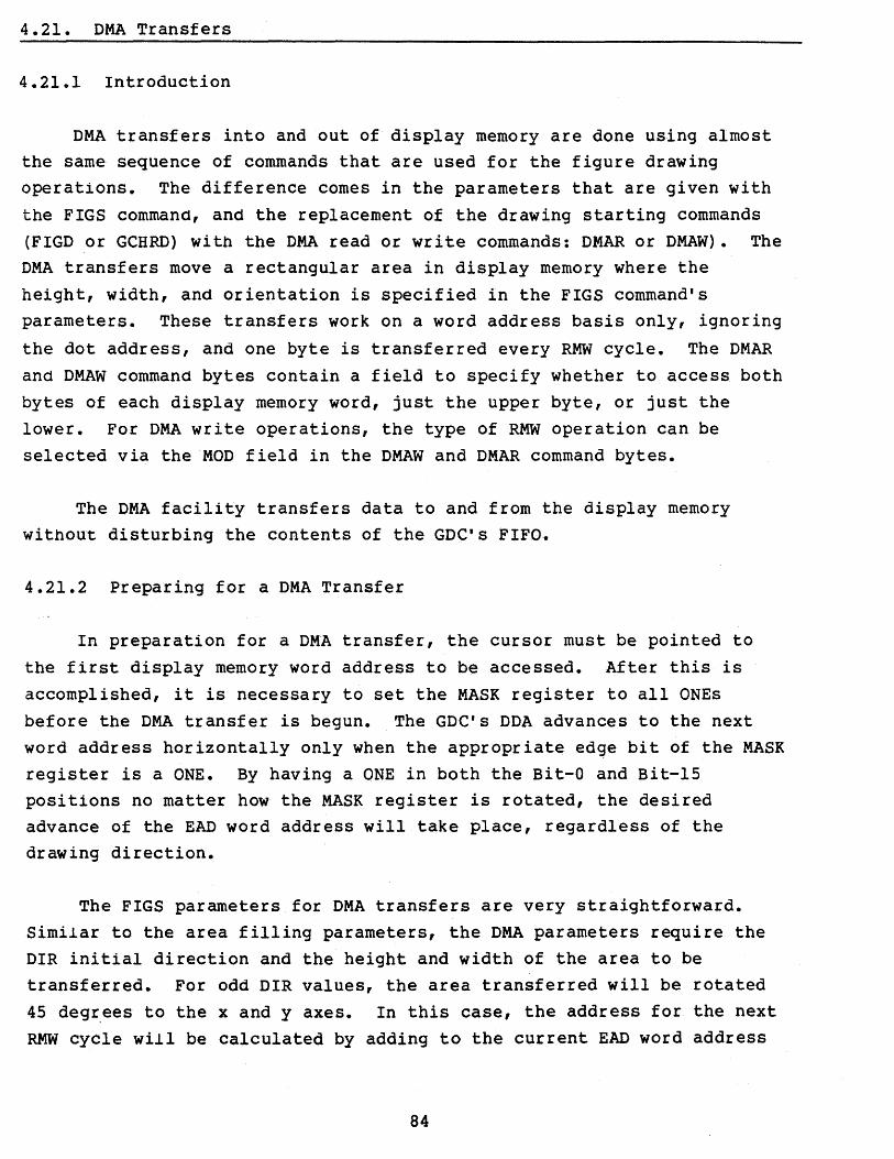
4.21. DMA Transfers
4.21.1 Introduction
DMA transfers into and out of display memory are done using almost the same sequence of commands that are used for the figure drawing operations. The difference comes in the parameters that are given with
the FIGS command, and the replacement of the drawing starting commands (FIGD or GCHRD) with the DMA read or write commands: DMAR or DMAW). The DMA transfers move a rectangular area in display memory where the height, width, and orientation is specified in the FIGS command's parameters. These transfers work on a word address basis only, ignoring
the dot address, and one byte is transferred every RMW cycle. The DMAR
and DMAW command bytes contain a field to specify whether to access both bytes of each display memory word, just the upper byte, or just the lower. For DMA write operations, the type of RMW operation can be selected via the MOD field in the DMAW and DMAR command bytes.
The DMA facility transfers data to and fr·om the display memory without disturbing the contents of the GDC's FIFO.
4.21.2 Preparing for a DMA Transfer
In preparation for a DMA transfer, the cursor must be pointed to
the first display memory word address to be accessed. After this is accomplished, it is necessary to set the MASK register to all ONEs before the DMA transfer is begun. The GDC's DDA advances to the next word address horizontally only when the appropriate edse bit of the MASK register is a ONE. By having a ONE in both the Bit-O and Bit-15 positions no matter how the MASK register is rotated, the desired advance of the EAD word address will take place, regardless of the drawing direction.
The FIGS parameters for DMA transfers are very straightforward. Similar to the area filling parameters, the DMA parameters require the DIR initial direction and the height and width of the area to be transferred. For odd DIR values, the area transferred will be rotated 45 deg~ees to the x and y axes. In this case, the address for the next RMW cycle will be calculated by adding to the current EAD word address
84
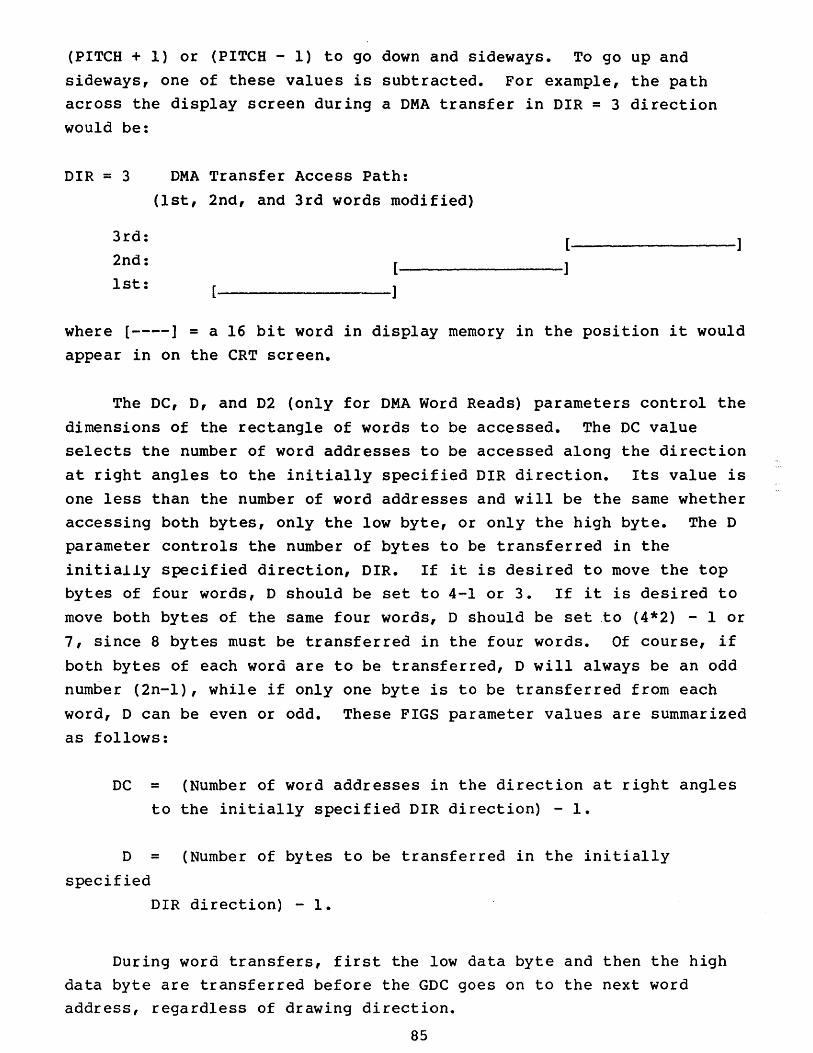
(PITCH + 1) or (PITCH - 1) to go down and sideways. To go up and
sideways, one of these values is subtracted. For example, the path across the display screen during a DMA transfer in DIR = 3 direction would be:
DIR = 3 DMA Transfer Access Path:
(1st, 2nd, and 3rd words modified)
3rd: [ 2nd: ] 1st: ]
where [----] = a 16 bit word in display memory in the position it would appear in on the CRT screen.
The DC, D, and D2 (only for DMA Word Reads) parameters control the
dimensions of the rectangle of words to be accessed. The DC value selects the number of word addresses to be accessed along the direction
at right angles to the initially specified DIR direction. Its value is one less than the number of word addresses and will be the same whether accessing both bytes, only the low byte, or only the high byte. The D parameter controls the number of bytes to be transferred in the
initially specified direction, DIR. If it is desired to move the top bytes of four words, D should be set to 4-1 or 3. If it is desired to move both bytes of the same four words, D should be set ,to (4*2) - 1 or
7, since 8 bytes must be transferred in the four words. Of course, if
both bytes of each word are to be transferred, D will always be an odd number (2n-l), while if only one byte is to be transferred from each
word, D can be even or odd. These FIGS parameter values are summarized as follows:
DC = (Number of word addresses in the direction at right angles to the initially specified DIR direction) - 1.
D = (Number of bytes to be transferred in the initially
specified
DIR direction) - 1.
During word transfers, first the low data byte and then the high data byte are transferred before the GDC goes on to the next word address, regardless of drawing direction.
85
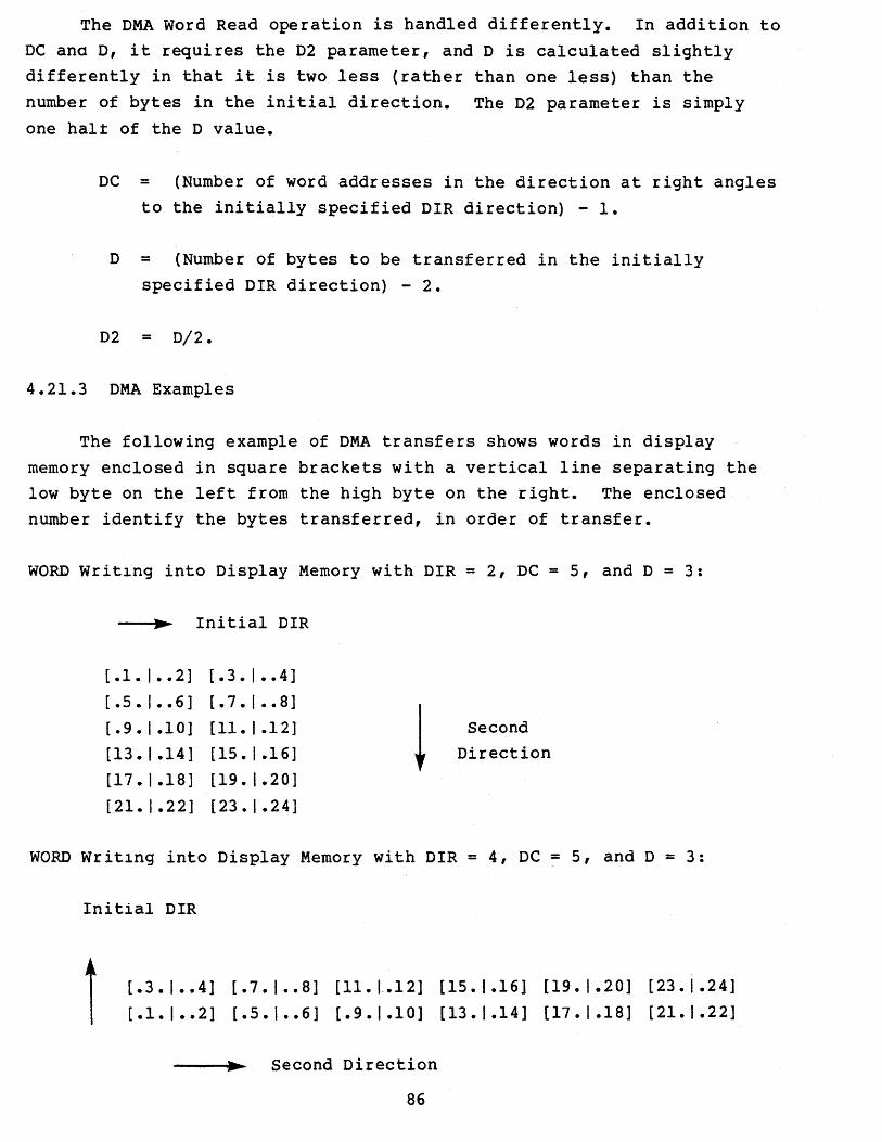
The DMA Word Read operation is handled differently. In addition to DC ana D, it requires the D2 parameter, and D is calculated slightly differently in that it is two less (rather than one less) than the number of bytes in the initial direction. The D2 parameter is simply one halt of the D value.
DC = (Number of word addresses in the direction at right angles to the initially specified DIR direction) - 1.
D = (Number of bytes to be transferred in the initially specified DIR direction) - 2.
D2 = D/2.
4.21.3 DMA Examples
The following example of DMA transfers shows words in display memory enclosed in square brackets with a vertical line separating the low byte on the left from the high byte on the right. The enclosed number identify the bytes transferred, in order of transfer.
WORD Writ~ng into Display Memory with DIR = 2, DC = 5, and D = 3:
--~.~ Initial DIR
[.1.1 •• 2] [.3.1 •• 4]
[.5.1 •• 6] [.7.1 •• 8]
! [.9.1.10] [11. I .12] Second
[13.1.14] [15. I .16] Direction
[17.1.18] [19.1.20]
[21.1.22] [23.1.24]
WORD Writ~ng into Display Memory with DIR = 4, DC = 5, and D = 3:
Initial DIR
i [.3.1 •• 4] [.7.1 •• 8] [11.1.12] [15.1.161 [19.1.20] [23.1.24] [.1.1 •• 2] [.5.1 •• 6] [.9.1.10] [13.1.14] [17.1.18] [21.1.22]
------~~ Second Direction
86
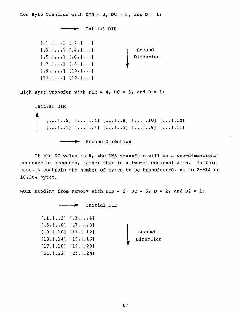
Low Byte Transfer with DIR = 2, DC = 5, and D = 1:
---I~~ Initial DIR
[.1./ ••• ] [.2./ ••• ]
[.3./ ••• ) [.4.1 ••• ]
! Second
[.5./ ••• ] [.6.1 ••• ] Direction
[.7./ ••• ] [.8.1 ••• ] [.9.1 ••• ] [10./ ••• ]
[11.1 ••• ] [12./ ••• ]
High Byte Transfer with DIR = 4, DC = 5, and D = 1:
Initial DIR
[ ••• 1 •• 2] [ ••• 1 •• 4] [ ••• 1 •• 8] [ ••• 1.10] [ ••• 1.12]
[ ••• 1 •• 1] [ ••• 1 •• 3] [ ••• 1 •• 5] [ ••• 1 •• 9] [ ••• 1.11]
----~~~ Second Direction
If the DC value is 0, the DMA transfers will be a one-dimensional sequence of accesses, rather than in a two-dimensional area. In this
case, D controls the number of bytes to be transferred, up to 2**14 or
16,384 bytes.
WORD Reading from Memory with DIR = 2, DC = 5, D = 2, and D2 = 1:
.. Initial DIR
[.1.1 •• 2] [.3.1 •• 4]
[.5.1 •• 6] [.7.1 •• 8]
t [.9.1.10] [11.1.12] Second
[13.1.14] [15.1.16] Direction
[17.1.18] [19.1.20]
[21.1.22] [23 • 1 .24]
87
WORD Reading from Memory with DIR = 4, DC = 5, D = 2, and D2 = 1:
Initial DIR
t [.3.1 •• 4] [.7.1 •• 8] [11.1.12] [15.1.16] [19.1.20] [23.1.24]
[.1.1 •• 2] [.5.1 •• 6] [.9.1.10] [13.1.14] [17.1.18] [21.1.22]
----~~~ Second Direction
4.21.4 Partial Word DMA Writes
It is possible to transfer data through DMA into the Display Memory and modify only some of the bits of each word accessed. If only the lower or upper eight bits are to be modified, the appropriate byte transfer mode can be used as described above. If an arbitrary number of bits must be modified, a different approach must be used.
Modifying an arbitrary pattern of bits in each word with DMA Word writes can be done one of two ways. With either technique, the Mask
register must be used to select which bits are to be modified. The trivial case is when only one word is to be modified. The more interesting case is when the vertical boundary of an area to be transferred into does not fallon a word boundary.
The key element in making partial word DMA writes into display
memory is the Mask register. In addition to enabling bit modification, the Mask register also works with the DDA to control the advancing of
the EAD word address. When the instantaneous direction of the next pixel to be drawn has a component along the x axis, the appropriate Mask
register edge bit is tested for a ONE to see if the end of the word has been reached. If it has, the EAD is advanced to the next word and the Mask register is rotated to point at the first bit to be modified in the
new word. If the end of the word has not been reached (the edge bit = ZERO), the Mask register is shifted to pOint to the next pixel in the current word.
This testing is done for all the drawing directions except straight
up ana down, in which there is no horizontal component. In these two directions, the EAD will be advanced after every RMW cycle, regardless of the Mask register contents and the Mask register will not be rotated.
88
To keep the DDA advancing only vertically throughout the duration of the DMA operation, a one-dimensional transfer must be programmed by the FIGS commana; the DC value must be O.
This mode of operation is perfect for DMA'ing data into the left and right boundary edges of a larger DMA rectangle. The area will have to be filled with three DMA operations: the left edge words, the center
rectangle of words, and the right edge words. In this way, an arbitrary rectangle can be DMA-filled on any bit boundary in the Display Memory.
4.22 Successive Address Accesses
The DDA can also be programmed to increment linearly through successive display memory addresses, in the specified direction. In this mode, the DDA steps through memory one address at a time, for as many accesses as are specified by the DC parameter of the FIGs command. The first parameter byte of the FIGS command sequence should have none of the Figure Type Select bits set for this mode, and only the DC
parameter need be sent to the GDC to specify the number of words to be
accessed. Any number of RMW cycles can be specified from 1 to 2**14 = 16,384.
This capability can be used to draw single pixels into the display memory or to access a number of words, for either reading or writing, in either graphics bit-mapped or coded character areas.
When preparing to do an operation involving one RMW cycle per word address, the Mask register must be set to all ONEs with a Mask command. This must be done after the cursor is positioned and before the FIGS commano. The DDA will then advance the EAD after each RMW cycle because both the LSB and the MSB of the Mask register will be ONE. An exception would be single pixel writing, when the CURS command will load the Mask register with one-of-sixteen bits.
4.23 Word Reading and Writing
Using the Successive Addresses mode, either or both bytes of each word can be accessed for word reading and writing. Unlike DMA transfers, the data is passed through the command and parameter FIFO, under the direct control of the host microprocessor. This is very
useful for initializing large amounts of display memory to the same
89
value, such as all ZEROs or all ONEs, without the overhead of setting up a DMA transfer. If .the DIR value is set equal to 2, the DDA will calculate a path through ascending addresses for as many words as the DC parameter calls for (DC = number of words - 1). As it crosses the end of a line of memory words, it will go to the next higher address, which is the first memory word of the next line. Each FIGS/WDAT command sequence can access 16,384 words, since the DC parameter has 14 bits.
This is the fastest way to clear display memory, because there is no interaction with the host system during 16K words of clearing. It is also a good way to read a range of memory during area flooding.
To use this mode it is necessary to pOint the 'cursor to the first word to be accessed and to set the Mask register to all ONEs. This allows the DDA to advance to the next word address after each RMW cycle, regardless of drawing direction.
The DC value specifies the number of words accessed, regardless of ' the number of bytes accessed per word.
In a graphics bit-mapped area, the WDAT command uses only the least significant bit of the parameter bytes which follow it. In a coded character situation, all the bits of the parameters are used for the RMW
operation.
In order to write a random pattern into a word in display memory it is necessary to use the Mask reg{ster to hold the pattern and pass all
ONEs to the DDA with a WDAT command. without an all ONEs value in the Mask register, the EAD will not advance properly to the next word address, except in the straight up and down drawing directions (DIR = 0 or 4), so the cursor must be set for each word.
For a WDAT command, the DC count of the FIGS command is used to
control the number of times the first set of parameter data is written into the display memory. This value is decremented in the process of doing these writes until a value of ZERO is reached. Subsequent sets of parameter data following the WDAT opcode will see DC values of O. For , example, if the FIGS command sets DC to 5 and three sets of data follow the WDAT opcode, the first set will be written into six different words while the second and third sets will be written once each into two additional locations.
90
4.24 GDC Command Sequence Examples
4.24.1 Introduction
These examples are typical of the operations done with the uPD7220
Graphics Controller ~n a bit-mapped graphics application. Many other operations are possible and reasonable. Many other modes of operation are possible also. The ones discussed here are intended to be
informative and to illustrate basic principles which can be applied to any situation.
Assumptions: - 5 MHz GDC clock
- 800 nsec per byte to load the FIFO
4.24.2 Minimum FIFO Load Times
The minimum FIFO load times give an idea of length of time required to get the command opcodes and their parameters into the GDC's FIFO. These numbers give an idea of how much time the loading process might take when compared to the parameter preparation time, and the execution time. These considerations are interesting when considering balancing the various components of your graphics system. For example, it
wouldn't make much sense to spend a large percentage of your system's cost on an advanced processor which could calculate vector drawing parameters in 2 usec when the GDC can only accept them over 12 usec. (Of course, if other jobs could be found for the processor to do during the remainder of the time, there might be a motivaton to do this.) The minimum load times have been calculated simply by multiplying the number of bytes to be transferred by 800 nsec per byte transferred. This assumes that the FIFO starts empty (and doesn't overflow) and that every other timing factor is optimal. Few if any real systems will achieve
sustained transfer rates at this speed.
4.24.3 Initialization (Master VSYNC Mode, Graphics Mode)
This command sequence needs to be done only after power up. The basic operation of the GDC is characterized to the individual application with these commands and parameters. Other modes of
91
operation will require different parameter bytes and considerations but will require the same commands.
- 22 bytes to load into the FIFO - Minimum FIFO load time of 17.6 usec
1. RESET Opcode
2. PI = mode bits 3. P2 = active words per line 4. P3 = VSYNC and HSYNC widths 5. P4 = HFPORCH and VSYNC widths 6. P5 = HBPORCH width 7. P6 = VFPORCH width 8. P7 = active lines per video field 9. P8 = VBPORCH width and active lines count
10. VSYNC Opcode + Master/Slave bit
11. PITCH Opcode
12. PI = display memory width
13. PRAM Opcode + PRAM starting address of 0 14. PI = display window starting word address, 15. P2 = display window starting word address, 16. P3 = window length low bits + starting top
17. P4 = mode bits + window length top bits
18. CCHAR opcode 19. PI = sweep lines per character row - 1 = 0
(for Graphics mode)
20. Zoom Opcode
low byte high byte bits
21. PI = display + writing zoom magnification factors
22. Start Opcode
4.24.4 Display Mode Change
This command is used to change the mode of operation without
resetting the Video Sync Generator or flushing the contents of the FIFO. Typically it is used to enter and exit Flash mode from Flashless mode as
92
drawing requirements change during interactive editing sessions, and to turn on and off the automatic dynamic RAM refresh to maximize the time available for drawing if the RAMs can be otherwise refreshed. The SYNC opcode can also be followed by the complete set of parameters accepted by the RESET command.
- 2 bytes to load into the FIFO
- Minimum FIFO load time of 1.6 usec
1. SYNC Opcode + DE bit
2. PI = mode bits
4.24.5 Blank the Screen
This command and the next are especially useful during Flashless Drawing mode to allow screen-clearing operations to proceed at Flash mode-like speeds. By blanking the screen, the GDC will be able to use
the entire video field for RMW operations instead of only the horizontal and vertical retrace blanking intervals. The HSYNC interval will
continue to be used for dynamic RAM refresh cycles, if so enabled, regardless of whether the screen is blanked or not. The 16 FIGS/WDAT word clearing command sequences needed to clear a 256K maximum display memory can be executed in under 250 msec using this technique (closer to one fifth of a second).
If the host processor system can keep the GDC busy doing figure
drawing, the initial drawing of the screen can be done at very high speed in Flash Drawing mode by blanking the screen during this period. Normal interactive drawing can be done in Flashless mode, without screen
disturbances and little impact on throughput, due to the low overall throughput requirements of direct interaction with the user.
During Flash Drawing mode operation it may be desirable to blank the screen for lengthy drawing operations rather than allow the user to see a highly disturbed display.
Additionally, a blanked screen can be used as part of the
interactive dialogue between the system and the user.
- 1 byte to load into the FIFO - Minimum FIFO load time of 0.8 usee
1. BCTRL Opcode + DE bit = 0 93
4.24.6 Unblank the Screen
This command sequence is the inverse of the screen blanking sequence described in section 4.24.5 - Blank the Screen.
- 1 byte to load into the FIFO
- Minimum FIFO load time of O.S usec
1. BCTRL Opcode + DE bit = 1
4.24.7 Drawing Setup
Before any drawing can be done, the drawing pattern and the RMW operation must be established. They need not be set again unless a
change is desired or a value is disturbed by another command. The drawing pattern is stored in the Parameter RAM by the appropriate PRAM
commana. Note that the locations in the Parameter RAM used by the drawing pattern (RA-S and 9) are also used by the area filling (graphics character) patterns (R-S through 15). Also note that several GDC commana opcodes have the RMW operation selecting field, MOD. The operation may be inadvertently changed during a DMA Read operation, for example, when the MOD field is otherwise of no concern.
- 4 bytes to load into the FIFO - Minimum FIFO load time of 3.2 usec
1. WDAT Opcode + transfer type + RMW operation code
2. PRAM Opcode + PRAM starting address of S
3. PI = drawing pattern, low byte 4. P2 = drawing pattern, high byte
4.24.S Cursor Positioning (Graphics mode)
All RMW operations, whether figure drawing, DMA transfers, or data reads ana writes, use the cursor position as their starting location.
Occasionally the cursor value from the previous operation will be correct for the next operation, but normally the cursor will have to be
reloaded with a new value for each RMW operation. For example, if done correctly, it is possible to chain vectors end-to-end without updating
94
the cursor between vectors. It is also convenient to do this with area filling and data reading and writing.
The cursor value in Graphics mode has two parts: the address of the word in memory (18 bits), and the address of the bit (pixel) within that word. The EAD (Execution Address) register holds the word address and the Mask register holds the dot address, dAD. Notice that the CURS
commana and the Mask command interact in that they both change the contents of the Mask register. The CURS command loads the Mask register
with the one-of-sixteen value which corresponds to the four-bit dAD
value of the fourth parameter byte.
- 4 bytes to load into the FIFO - Minimum FIFO load time of 3..2 usec
1. CURS Opcode
2. PI = Word Address, EAD - (0 through 7)
3. P2 = Word Address, EAD - (8 through 15)
4. P3 = [Dot Address, dAD (0 through 3)] + [EAD - (16 through 17)]
4.24.9 Mask Register Loading
The Mask command loads the Mask register with the 16-bit value
specified by its parameter bytes. This command should only follow the CURS command since the dot address, dAD, will overwrite any previous contents of the Mask register.
- 3 bytes to load into the FIFO
- Minimum FIFO load time of 2.4 usec
1. MASK Opcode 2. PI = Least significant byte of MASK Pattern 3. P2 = Most significant byte of MASK Pattern
4.24.10 Vector Drawing
This command sequence positions the cursor to the figure's starting
pixel address in display memory, sets up the Digital Differential
Analyzer (DDA), and initiates the drawing process. It is not necessary
95
to load the cursor address if the previous operations have left it at the starting point of the desired vector.
- 15 bytes to load into the FIFO - Minimum FIFO load time of 12.0 usec - Execute time for 100 pixels = 80 usec
1. CURS Opcode
2. PI = Word Address EAD - (0 through 7) 3. P2 = Word Address EAD - (8 through 15) 4. P3 = Dot Address dAD - (0 through 3) + EAD - (16 through 17)
5. FIGS Opcode
6 • PI = Type = 00000 (Binary) + DIR 7. P2 = GD Bit + DC low byte 8. P3 = DC high byte 9. P4 = D low byte
10. P5 = D high byte 11. P6 = D2 low byte
12. P7 = D2 high byte
13. P8 = D1 low byte
14. P9 = Dl high byte
15. FIGD Opcode to start drawing process
4.24.11 Single Dot Writing
When drawing just a single pixel (or word) it is not necessary to supply all the DDA parameters, since it will be doing only the first RMW
operation. The number of bytes sent to the GDC can, therefore, be
reduced.
- 7 bytes to load into the FIFO - Minimum FIFO load time of 5.6 usec
1. CURS Opcode
2. PI = Word Address EAD - (0 through 7)
3. P2 = Word Address EAD - (8 through 15)
4. P3 = Dot Address dAD -:- (0 through 3) + EAD - (16 through 17)
5. FIGS Opcode
96
6. PI = Type = 00000 (Binary) + DIR
7. FIGD Opcode to draw the dot
4.24.12 Arc Drawing
The considerations for this command are similar to those of vector
drawing. See section 4.24.10.
- 17 bytes to load irito the FIFO
- Minimum FIFO load time of 13.6 usec
1. CURS Opcode
2. PI = Word Address EAD - (0 through 7)
3. P2 = Word Address EAD - (8 through 15)
4. P3 = Dot Address dAD - (0 through 3) + EAD - (16 through 17)
5. FIGS Opcode
6. PI = Type = 00100 (Binary) + DIR
7. P2 = GD Bit + DC low byte 8. P3 = DC high byte
9. P4 = D low byte
10. PS = D high byte
11. P6 = D2 low byte
12. P7 = D2 high byte 13. P8 = D1 low byte 14. P9 = Dl high byte 15. P10= DM low byte 16. P1l= DM high byte
17. FIGD Opcode to start the drawing process
4.24.13 Area Filling/Graphics Characters (Random Sizes)
This command sequence is useful for filling random-sized areas on the screen and for writing into the bit-map characters which are other than 8 by 8 bits. A random area of up to 2**14 (16,384) pixels along each edge can be filled with one command sequence. The area will be filled mozaic-style from the pattern loaded into the Parameter RAM by replicating the pattern in both the x and y dimensions. When drawing
bit-mapped characters which exceed 8 bits in either direction, it will
97
be necessary to reload the Parameter RAM for the bits outside the basic 8 by 8 square.
When drawing 7 by 9 characters in a 9 by 11 (or larger) window, it is not necessary to reload the Parameter RAM to. draw the extra column of bits beyond the first eight bits of the character window's width. The
9th bit of the character window's width can be written as a repeat of the first bit in the row. The first bit of each row will always be ZERO since they are the "guard U bits of the window around the actual
character. In this case, the GDC would be programmed to draw a 9-bit
wide area and it will use this first ZERO bit in both the first and ninth positions. The rows of character after the eighth will, of course, require the reloading of a part of the Parameter RAM.
Setup for this command requires the establishment of the RMW operation, and the Writing Zoom factor.
Be sure that the last pattern byte to be loaded with the PRAM
command goes into location 15 of the Parameter RAM, since this is where the GDC will get its first byte of information for the filling process.
If the drawing direction and orientation of the pattern bits are coordinated, a succession of drawing operations can be made without reestablishing the cursor position.
Relative order of the CURS and PRAM commands is unimportant and is often dictated by the application's requirements.
- 13 bytes + extra PRAM bytes to load into the FIFO . - Minimum FIFO load time of 10.4 usee + 0.8 usec for each extra
PRAM byte after the first
1. CURS Opcode 2. PI = Word Address EAD - (0 through 7) 3. P2 = Word Address EAD - (8 through 15) 4. P3 = Dot Address dAD - (0 through 3) + EAD - (16 through 17)
5. PRAM Opcode + PRAM Starting Address 6. PI through Pn Pattern bytes
98
7. FIGS Opcode
8. PI = Type = 00010 (Binary) + DIR (Type = 10010 for Slanted)
9. P2 = GD Bit + DC low byte
10. P3 = DC high byte 11. P4 = D low byte
12. PS = D high byte
13. GCHRD Opcode to start area filling process
4.24.14 Area Filling/Graphics Character (8 by 8)
Refer to the comments for the random area filling sequence (section 4.24.13). Similar considerations apply to this command sequence.
- 17 bytes to load into the FIFO
- Minimum FIFO load time of 13.6 usec
- Execute time )=64 * .8 = Sl.2 usec
1. PRAM Opcode + PRAM Starting Address of 8 2. PI = Pattern byte 8. Last drawn 3. P2 = Pattern byte 9 4. P3 = Pattern byte 10 S. P4 = Pattern byte 11 6. PS = Pattern byte 12
7. P6 = Pattern byte 13
8. P7 = Pattern byte 14 9. P8 = Pattern byte IS. Drawing starts with Bit-O
10. CURS Opcode
11. PI = Word Address EAD - (0 through 7) 12. P2 = Word Address EAD - (8 through IS)
13. P3 = Dot Address dAD - (0 through 3) + EAD - (16 through 17)
14. FIGS Opcode
15. PI = Type = 00010 (Binary) + DIR (Type = 10010 for Slanted)
16. P2 = GD Bit + DC low byte
17. GCHRD Opcode to start area filling process
99
4.24.15 Rectangle Drawing
The considerations for this operation are similar to those for vector drawing. See section 4.24.10.
- 17 bytes to load into the FIFO - Minimum FIFO load time of 13.6 usee
1. CURS Opcode 2. PI = Word Address EAD - (0 through 7) 3. P2 = Word Address EAD - (8 through 15) 4. P3 = Dot Address dAD - (0 through 3) + EAD - (16 through 17)
5. FIGS Opcode
6. PI = Type = 01000 (Binary) + DIR 7. P2 = GD Bit + DC low byte
8. P3 = DC high byte
9. P4 = D low byte 10. P5 = D high byte
11. P6 = D2 low byte
12. P7 = 02 high byte 13. P8 = Dl low byte
14. P9 = Dl high byte
15. PI0 = DM low byte 16. Pil = DM high byte
17 • FIGD Opcode to start the drawing process
4.24.16 Pan and Scroll the Display Window
Changing a display partition window starting address will cause the window to roam around in the larger display memory. The display memory
may be larger than the display window in either or both the x and y directions. It is a good idea to change the window starting address
after VSYNC has ended and before active video begins, so that the GDC's Commana Processor will not access a half new, half old value when it
goes to the Parameter RAM for the address for the display scanning
process. The Vertical Back Porch is an ideal time to do this modification, because the first partition's parameters have already been accessed but there is no chance of the second partition's values being
100
needed until later. The Vertical Back Porch time can be found by testing the VSYNC status register for a falling edge.
- 3 bytes to load into the FIFO - Minimum FIFO load time of 2.4 usec
1. PRAM Opcode + PRAM starting Address of 0, 4, 8, or 12 2. PI = Display Partition Starting Address, low byte
3. P2 = Display Partition Starting Address, high byte
4.24.17 Zoom Factor Change
Since the display zoom factor is passed into the GDC in a single byte, the same timing precautions need not be heeded for changing the display partition starting addresses. The writing zoom factor can be
changed at any time. The external Zoom Pixel Pre-scaler counter must also be set to correspond to the zoom factor given to the GDC.
- 2 bytes to load into the FIFO
- Minimum FIFO load time of 1.6 usee
1. ZOOM Opcode 2. PI = Display Factor + writing Factor
4.24.18 Set Background
This command sequence is used to initialize large areas of display memory. Simple incremental advancing is done to calculate the next word address in display memory. Note that the setting of the Mask register
to all ONEs forces the DDA always to increment the EAD word address after each RMW cycle, and the RMW Logic unit to modify all the bits of each word. It is typical to use the Set, Clear, Replace RMW operations when clearing or setting memory. Also note that in Graphics mode, this sequence can be used only to set or clear all the bits of each word accessed to the same value (Bit-O of the WDAT parameter).
101
If more than 16,384 successive words are to be accessed, there is no need to re-establish the cursor and mask values for each FIGS/WDAT commana pair.
- 14 bytes to load into the FIFO to fill up to 16,384 words - Minimum FIFO load time of 11.2 usec - Execute time of )=13.107 msec for a 16,384 word block - 7 bytes to fill additional successive areas, each up to 16,384
words long
1. CURS Opcode
2. PI = Word Address EAD - (0 through 7) 3. P2 = Word Address EAD - (8 through 15) 4. P3 = Dot Address dAD - (0 through 3) + EAD - (16 through 17)
5. MASK Opcode
6. PI = FF (HEX)
7. P2 = FF (HEX)
Repeat
8. FIGS Opcode
9. PI = Type = 00000 (Binary) + OIR 10. P2 = GO Bit + DC low byte 11. P3 = DC high byte
12. WDAT Opcode + Transfer Type + RMW Operation 13. PI = Pattern data, low byte (Only Bit-O used) 14. P2 = Pattern data, high byte
until
4.24.19 Multi-Pixel write
In Graphics mode by using the Mask register to hold the pattern data, any pattern of bits may be written into a display memory word in
~
one RMW cycle. A dummy pattern is passed as parameters of the WDAT command and must have a ONE in Bit-O of the low byte to allow the desired pattern in the Mask register to express itself in every bit pOSition. Since the Mask register also controls whether the OOA increments the EAD address, an arbitrary mask pattern will not always
102
·executed once, since no relevant parameter is changed during this mode of operation. This command will not perform Replace operation because
the bit pattern in the Mask Register is used only as masking bits, not as new data. To perform Replace function the word would have to be
first cleared in the video memory.
- 12 bytes to load into the FIFO for the first word - Minimum FIFO load time of 9.6 usec for the first word - 10 bytes to load into the FIFO of each succeeding word - Minimum load time of 8.0 usec for each succeeding word
1. FIGS Opcode
2. PI = TYPE = 00000 (Binary) + DIR
Repeat
3. CURS Opcode
4. PI = Word Address EAD - (0 through 7) 5. P2 = Word Address EAD - (8 through 15) 6. P3 = Dot Address dAD - (0 through 3) + EAD - (16 through 17)
7. MASK Opcode
8. PI = Pattern, low byte
9. P2 = Pattern, high byte
10. WDAT Opcode + Transfer Type + RMW Operation
11. PI = FF (HEX), Dummy pattern low byte
12. P2 = FF (HEX), Dummy pattern high byte
Until
4.24.20 Reading Data From the Display Memory
The contents of Display Memory can be read to the host processor through the FIFO in a linear sequence of addresses of up to 16,384
locations. Any linear direction may be selected from the eight selected
by the DIR parameter of the FIGS command. After the cursor is set with the CURS command, it is necessary to set the"Mask Register to all ONEs for all DIR directions other than a and 4 to ensure the proper incrementation of the EAD word address. The GDC's FIFO will be turned around from Write mode to Read mode when the RDAT command is executed.
103
Any commands or parameters which followed RDAT command into the FIFO will be lost as the read operation begins.
The GDC will begin to do RMW memory cycles to read the requested
data soon after the RDAT opcode is executed. The data is loaded into
the FIFO byte by byte as it becomes available. After the first byte is in the FIFO, the GDC's Data register is loaded with the top byte on the
FIFO and the DATA READY flag in the status register will be set. The host processor may then read the data at GDC port address 1. GDC internal hardware then gets the next byte from the FIFO, if available, and into the Data register, etc. It is important for the host processor to check the DATA READY status bit before each read, because the FIFO is implemented as a ring buffer RAM and time is required to access its contents. The peak transfer rate from the FIFO will yield a byte from the FIFO every four 2xWCLK cycles, which is the same rate at which the
FIFO is filled via RMW memory cycles. Actual transfer rates will be
lower in flashless mode since the RMW cycles cannot be done during much of the video field time.
The GDC will continue to fetch data from the Display Memory into the FIFO until the DC value decrements to zero. These RMW read cycles
will pause if the FIFO is full, until the host processor makes more room in the FIFO by reading data.
The host processor may abort the read sequence before the total number of words has been accessed by outputting a command byte to the
GDC. The FIFO is then forced into write mode to accept and normally process the command output operation and its following parameters. Note that the command output operation, in this situation, should not check the Status register FIFO FULL bit before outputting the command byte. The FIFO may well be full of read data as the command is about to be output. All read data in the FIFO at the time a command byte is received will be lost when the FIFO turns around.
- 12 bytes to load into the FIFO to initiate a sequence of words to be read
- Minimum of 9.6 usec to initiate the read operation
1. CURS Opcode
2. PI = Word Address EAD - (0 through 7) 3. P2 = Word Address EAD - (8 through 15)
104
4. P3 = Dot Address dAD - (0 through 3) + EAD - (16 through 17)
5. MASK Opcode
6. PI = FF (HEX)
7 • P2= FF (HEX)
8. FIGS Opcode
9. PI = Type = 00000 (Binary) + DIR 10. P2 = GD Bit + DC low byte
11. P3 = DC high byte
12. RDAT Opcode + Transfer Type + RMW Operation
4.24.21 DMA Data Writing
Display Memory data can be written via the GDC's DMA interface once the GDC is set up for the transfer. The external DMA controller must
also have been programmed for the operation. Once the cursor is pointed to the starting pOint of the block to be transferred, the Mask register must be filled with all ONEs to insure that the EAD word address will be. properly advanced as the DMA transfer progresses. The FIGS command is used to set the TYPE, DIR, DC, and D values. After the DMAW opcode is
executed by the GDC's Command Processor, the DREQ pin will signal the start of the transfer. Any commands which followed the DMAW opcode into
the FIFO will not be lost during the DMA transfer since the DMA data
bypasses the FIFO. The Status register may be read while DREQ is
asserted, as long as DACK/ is not asserted. No commands should be
loaded into the GDC while the DMA Execute status register bit is high.
- 14 bytes to load into the FIFO to initiate the transfer
- Minimum of 11.2 usec to set up for the DMA transfer
1. CURS Opcode
2. PI = Word Address EAD - (0 through 7)
3. P2 = Word Address EAD - (8 through 15)
4. P3 = Dot Address dAD -(0 through 3) + EAD - (16 through 17)
5. MASK Opcode 6. PI = FF (HEX) 7 • P2 = FF (HEX)
105
8. FIGS Opcode 9. PI = Type = 00000 (Binary) + DIR
10. P2 = GD Bit + DC low byte
11. P3 = DC high byte
12. P4 = D low byte
13. PS = D high byte
14. DMAW Opcode + Transfer Type + RMW Operation
4.24.22 DMA Data Reading
The comments made for DMA writing also apply for DMA reading
(section 4.24.21).
1. CURS Opcode
2. PI = Word Address EAD - (0 through 7)
3. P2 = Word Address EAD - (8 through 15)
4. P3 = Dot Address dAD - (0 through 3) + EAD - (16 through 17)
S. MASK Opcode 6. PI = FF (HEX)
7. P2 = FF (HEX)
8. FIGS Opcode
9. PI = Type = 00000 (Binary) + DIR
10. P2 = GD Bit + DC low byte
11. P3 = DC high byte
12. P4 = D low byte
13. PS = D high byte
14. DMAR Op'code + Transfer Type + RMW Operation
106
4.25 Initia11zing the GDC
After power-up, the GDC must be initialized by a series of commands and parameters to configure it for the desired mode of operation. The host microprocessor will output this list of commands and their parameters as part of its power-up routine. Other than checking the GDC
FIFO's status to prevent FIFO overflow, only the transfer of fixed values into the GDC is necessary. Once the GDC or GDCs are initialized, the START command starts the display process.
Several commands must be given to the GDC to configure it for the desired operating mode. They are introduced here and are fully
explained in the data sheet.
4.25.1 Initia11zing Command Sequence
a. RESET puts the GDC into the Idle mode and prepares it to accept commands and parameters
b. SYNC configures the Video Sync Generator and operating modes. (These parameters may follow the RESET command without the SYNC
command byte). c. VSYNC specifies Master or Slave video operation. d. CCHAR sets up the Lines-Per-Row and Cursor Blink Rate values. e. PITCH establishes the width of the Display Memory.
f. PRAM loads the Parameter RAM with the desired display starting addresses and lengths.
g. ZOOM sets the display zoom factor. h. CURS positions the cursor, which is especially important
during initialization of character display modes.
Other than the RESET command which must come first, the order in which these commands are given is not important since they do not
interact with each other. The GDC will be in the Idle mode until a START command is issued. During Idle mode the display will be blanked,
and the video timing of any slave mode GDCs will synchronize to their master GDC or external sync source. During this synchronization process, the master GDC's Video Sync Generator will produce and output both horizontal and vertical sync signals, while the slave GDC or GDCs
will use their VSYNC pin as an input for this externally generated vertical sync signal. At the end of each VSYNC pulse the slaves will
reset their sync generators to line up with the external signal from the
107
master sync source. During Idle mode, all-GOCs will generate non-interlaced video whether or not interlaced video was specified. Once Idle mode ends via a START command, all the GOCs will be generating
the same video field of the video frame sequence. Once initialized as above, the GOC can accept and execute any of its other commands. The
Idle mode is ended by a START command, which stops the Video Sync Generator from synchronizing to the external vertical sync signal, and unblanks the display raster.
Once these commands have initialized the GOC, but before the START command, you may wish to clear the display memory using the techniques
discussed in the Figure Drawing section, which can clear the memory very quickly. If the GOC is being operated in Slave mode, it will need time to synchronize to the master sync source before the display START command is given. The host microprocessor should watch the VSYNC status
bit of the master GDC to insure that at least one complete VSYNC pulse reaches the slave GDC.
4.25.2 Special Considerations for the RESET Command
The first command to send to the GDC is the RESET command. It is interpreted by special hardware ahead of the FIFO to ensure that, whatever the power-up status of the Command Processor is, RESET will prepare it to accept the command and parameter protocol. The reset operation will also initialize and empty the FIFO, and initialize various internal counters.
The RESET command byte may be followed by the parameters that set up the Video Sync Generator and the basic operating mode. Alternately,
after the RESET command has been given, the SYNC command byte can precede these same parameters (without initializing the GOC again).
It is not a good idea to check the FIFO Full status bit before outputting the RESET command, since the FIFO may have powered up with the FIFO Full bit set. With the Command Processor waiting for its first command from the FIFO it assumes is empty, the FIFO will never become empty from the point of view of the host microprocessor. Of course, , after the RESET command, the FIFO Full bit should be checked before each byte is load~d into the FIFO. (It is possible to imagine a GOC driver
program sophisticated enough to check the FIFO Empty bit and do its own byte transfer counting but the speed gained would not offset the
increased complexity of such a routine).
108
CHAPTER 5 Host Interface
5.1 The FIFO Buffer
5.1.1 Introduction
The main pathway for information flow between the host microprocessor and the GDC is the First-In-First-Out (FIFO) buffer internal to the GDC. Commands and parameters are loaded into the buffer by the host and removed at the other end by the GDC's Command Processor.
With this technique, the host can load the commands and parameter bytes as they become available. The GDC Command Processor then handles them when it finishes execution of the previous command. In this way, the interface between these two asynchronous system elements is made more
efficient. If not for this low-overhead technique, this interface could be a major performance bottleneck. In addition, the FIFO is used to
buffer data for the host as it is read from the display memory or internal registers.
As is true with all FIFOs, the length of the GDC's FIFO is limited,
and if data is output when the FIFO is full, the oldest data in the FIFO will be overwritten and lost. When the host is doing reads from the FIFO, the data is moved from the FIFO into a temporary data register to allow fast access times onto the system data bus. The possibility of a
problem transferring data can be eliminated by checking the status bits which report on the condition of the FIFO and Data Register. An
additional overriding concern is the maximum speed at which the FIFO can tra'nsfer data. A byte of data can be transferred no more often than
once every four 2xWCLK cycles, even if the FIFO is not full or the Data Register ready.
5.1.2 FIFO status Bits
Three bits relating to the FIFO can be read in the GDC's status register: FIFO EMPTY, FIFO-FULL, and DATA-READY. The names of these bits describe their ONE state condition. For example, the FIFO-FULL bit is ZERO when the FIFO is not full. The two FIFO status bits are meaningful whether the data is flowing from the host into the GDC or the
reverse. The DATA-READY bit is used only for data reads out of the GDC. None of these bits are meaningful before the first RESET command opcode
is sent to the GDC after power-up.
109
5.1.3 FIFO Operation Modes
When commands and parameter bytes are being written into the GDC, the FIFO is in Data Write mode. After one of the commands which requests data from the GDC is executed, the FIFO is turned around into Data Read mode. Bytes of data are then read from the Data register,
which is in turn filled from the FIFO. The host processor must check the DATA-READY status bit before each read operation. The FIFO will
automatically resume Data Write mode operation, whether all the data is read or not, when a command byte is output to the GDC. Turn-arounds of
the FIFO to either mode will completely empty the FIFO of any contents.
5.1.4 Command and Data Transfer Through the FIFO
The normal sequence of events involve a large number of command and parameter writes {being careful that the FIFO does riot overflow}, and
occasional data reads {being sure that there is data available}. The light pen address, the cursor position, and data from the display memory
can all be read.
During the command and parameter outputting phase, the host processor works to keep the FIFO as full as possible without causing a
data overflow. When data must be read from the GDC, the host processor puts the appropriate command sequence into the FIFO like any other command. It then pauses and waits for the DATA-READY status bit to go HIGH. While it is waiting, the Command Processor empties the FIFO of
all the commands and parameters which preceeded the data read command.
The read command opcode byte is then fetched from the FIFO and decoded. The FIFO is next turned around and Data Read mode is entered. There is no lost data during the turn-around operation because nothing was loaded into the FIFO after the read data command opcode.
The GDC then proceeds to fetch the requested data for loading into
the FIFO. If the data is coming from the display memory and the Flashless mode has been selected, there can be delays during the active dispiay time until the GDC can get the first data byte into the FIFO. The FIFO is then filled as fast as the requested data can be accessed.
If the data is coming from the on-chip registers {the cursor or the light pen} the FIFO will be loaded without delay.
110
After the first byte is put into the FIFO, the process of sending the data to the host processor begins. The data is removed from the host side of th~ FIFO one byte at a time into the Data register. For each byte the DATA-READY status bit is set to a ONE. The host processor tests this bit until the data is ready and then reads the byte. The DATA-READY bit must be checked before the next byte can be read from the Data register. If there is data waiting in the FIFO to be read, the GDC
needs four 2xWCLK cycles to load each byte into the Data register.
The number of bytes to be transferred is determined either implicitly (for the cursor or light pen reads) or explicitly (by the
FIGS command for memory reads) before the transfer begins. The host processor has the option to abort the transfer sequence at any point by
simply outputting any command opcode byte to the GDC.
5.1.5 Considerations for Testing the Status Bits
After power up, the status bits are not meaningful until the RESET opcode is output to the GDC. The RESET will empty the FIFO, initialize
the status bits, and prepare the FIFO to receive further data. The RESET opcode is decoded by dedicated hardware ahead of the FIFO, instead
of by the Command Processor after passing through the FIFO. It is important not to check the FIFO-FULL bit before outputting the RESET opcode. The problem is that the FIFO control logic may have powered up, indicating a full FIFO, so that the status bit will never go LOW until the RESET command is given.
During outputs to the GDC, the FIFO must not be overflowed. There are two approaches for preventing this. The first is to check the
FIFO-FULL status bit for a ZERO before outputting each command and parameter byte. The second technique is to wait for the FIFO to become
empty and then send 16 bytes or less, in sequence, to the GDC. Of
course, the maximum transfer rate of one byte every four 2xWCLK cycles must not be exceeded. It is not a good idea to assume the GDC will be able to take more than 16 bytes, hoping the Command Processor will
remove a few bytes while the others are being loaded. The problem comes up when the GDC is busy doing a figure drawing, for example, and takes nothing from the FIFO for long periods of time while it draws.
During data reads from the GOC, the DATA-READY status bit must be checked before each read operation. The internal structure of the GDC
III
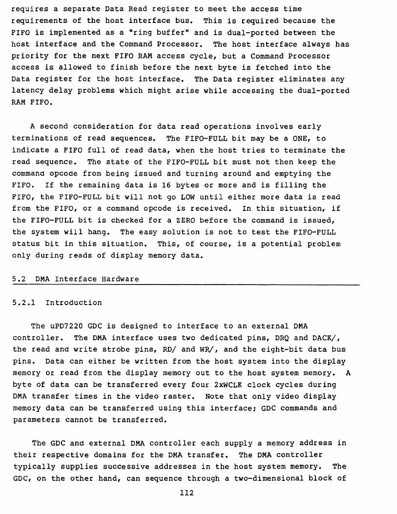
requires a separate Data Read register to meet the access time requirements of the host interface bus. This is required because the
FIFO is implemented as a "r ing buffer" and is dual-.ported between the host interface and the Command Processor. The host interface always has priority for the next FIFO RAM access cycle, but a Command Processor access is allowed to finish before the next byte is fetched into the Data register for the host interface. The Data register eliminates any latency delay problems which might arise while accessing the dual-ported RAM FIFO.
A second consideration for data read operations involves early
terminations of read sequences. The FIFO-FULL bit may be a ONE, to
indicate a FIFO full of read data, when the host tries to terminate the read sequence. The state of the FIFO-FULL bit must not then keep the commano opcode from being issued and turning around and emptying the FIFO. If the remaining data is 16 bytes or more and is filling the
FIFO, the FIFO-FULL bit will not go LOW until either more data is read from the FIFO, or a command opcode is received. In this situation, if
the FIFO-FULL bit is checked for a ZERO before the command is issued, the system will hang. The easy solution is not to test the FIFO-FULL status bit in this situation. This, of course, is a potential problem only during reads of display memory data.
5.2 DMA Interface Hardware
5.2.1 Introduction
The uPD7220 GDC is designed to interface to an external DMA controller. The DMA interface uses two dedicated pins, DRO and DACK/, the read and write strobe pins, RD/ and wR/, and the eight-bit data bus
pins. Data can either be written from the host system into the display memory or read from the display memory out to the host system memory. A byte of data can be transferred every four 2xWCLK clock cycles during DMA transfer times in the video raster. Note that only video display memory data can be transferred using this interface; GDC commands and parameters cannot be transferred.
The GDC and external DMA controller each supply a memory address in their respective domains for the DMA transfer. The DMA controller typically supplies successive addresses in the host system memory. The GDC, on the other hand, can sequence through a two-dimensional block of
112
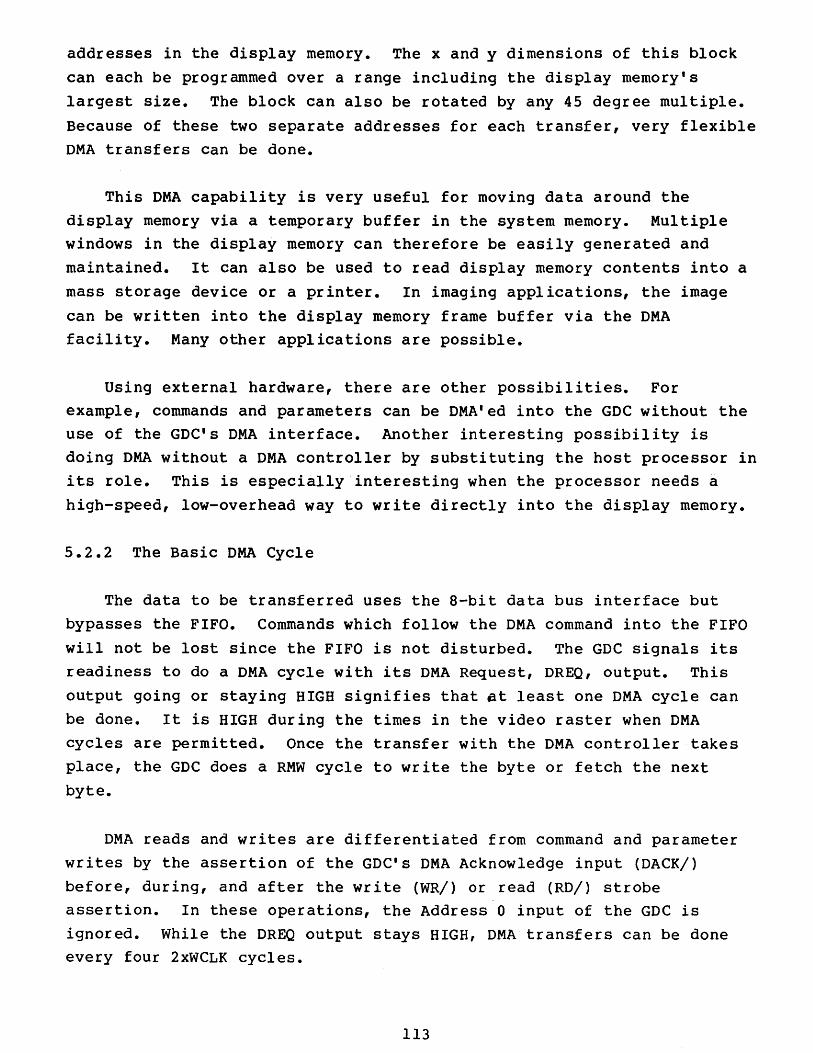
addresses in the display memory. The x and y dimensions of this block
can each be programmed over a range including the display memory's largest size. The block can also be rotated by any 45 degree multiple.
Because of these two separate addresses for each transfer, very flexible DMA transfers can be done.
This DMA capability is very useful for moving data around the display memory via a temporary buffer in the system memory. Multiple windows in the display memory can therefore be easily generated and maintained. It can also be used to read display memory contents into a mass storage device or a printer. In imaging applications, the image
can be written into the display memory frame buffer via the DMA facility. Many other applications are possible.
Using external hardware, there are other possibilities. For example, commands and parameters can be DMA'ed into the GDC without the use of the GDC's DMA interface. Another interesting possibility is doing DMA without a DMA controller by substituting the host processor in its role. This is especially interesting when the processor needs a high-speed, low-overhead way to write directly into the display memory.
5.2.2 The Basic DMA Cycle
The data to be transferred uses the 8-bit data bus interface but bypasses the FIFO. Commands which follow the DMA command into the FIFO
will not be lost since the FIFO is not disturbed. The GDC signals its readiness to do a DMA cycle with its DMA Request, DREQ, output. This output going or staying HIGH signifies that at least one DMA cycle can be done. It is HIGH during the times in the video raster when DMA cycles are permitted. Once the transfer with the DMA controller takes place, the GDC does a RMW cycle to write the byte or fetch the next byte.
DMA reads and writes are differentiated from command and parameter writes by the assertion of the GDC's DMA Acknowledge input (DACK/) before, during, and after the write (WR/) or read (RD/) strobe assertion. In these operations, the Address 0 input of the GDC is ignored. While the DREQ output stays HIGH, DMA transfers can be done every four 2xWCLK cycles.
113
Once a DMA sequence has been initiated by the host processor, the
GDC will assert its DREQ output during the AW interval of lines in which
DMA is permitted, until the requested number of transfers has been made.
The Vertical Back Porch (VBP) lines will always be used, as will the Active Lines (AL) if Flash mode has been selected.
Because of the restricted time intervals during which DREQ is asserted, only the DMA-EXECUTE status bit can be used to determine when the total DMA operation is finished. While a DMA operation is executing, the host should not put more commands into the GDC FIFO. The only interaction with the GDC, beyond the DMA transfers, should be to read the status register.
5.2.3 DMA Cycle Minimum Length
When a partial rectangle area of video memory is selectively specified for the DMA transfer, and the DMA transfer is performed one
byte at a time:
1 DMA cycle = 5 * TCLK
In other cases (when the transfer is in 16 bit words):
1 DMA cycle = 4 * TCLK
5.2.4 Timing Considerations for the DMA Transfer
The following timings, Tl and T2, should be noted.
DMA WRITE: WR (CMAW)
\ ___ T '~Tll
2XWCLK~
HSYNC 'r ______ ----J
Figure 5.1 DMA write Timing
DMA READ: DACK ~ I (DHAR) _I
TZi
2XWCLK~
HSYNC ~ -----Figure 5.2 DMA Read Timing
114
The following timing requirement should be met in relation to TI and T2. If Tl is met, T2 will be met automatically.
TI, T2 2. TCLK
From this timing requirement, the following timing considerations become necessary.
When the clock frequency of the GDC is the same as that of the DMA
controller, and the device that requests DMA transfer is only the GDC:
HFP 2. 3 characters
(or 2 characters when the matching of clock phase is good between the GDC and the DMA controller)
The reason for this requirement is as follows.
EXAMPLE: HFP = 1 character (2 clocks), GDC clock = DMA clock
DMA CYCLE 51 I 50 I 51 I 52 I S3 I 54 I 51 I 2xWCLK (GDC)
DREQ
\
HLDA
HBLANK
\ 3 clock. "-y ____ -+----
DMADATA ~ (Internal Data_B_US_) ___________ ~ H5YNC •
Data Contention
Internal Data ~
Bus Timing ___ ------------v/AV/#/k (Frame Enable INT)
Figure 5.3 DMA Timing Waveforms
In addition to the previous considerations, the followng external circuit may be necessary, depending on the system configuration.
115
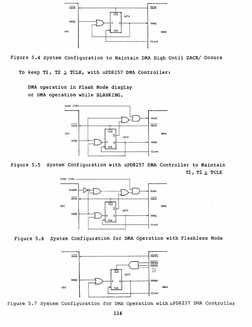
OACK i5AcK
LS74
OREQ OREQ
GDC DMAC
Clock
Figure 5.4 System Configuration to Maintain DMA High until DACK/ Occurs
To keep TI, T2 L TCLK, with uPD8257 DMA Controller:
DMA operation in Flash Mode display
or DMA operation while BLANKING.
HLDA (CPU)------------.,
HLDA
DACK I----+----~-t__-----, DACK
GOC
OREQ ~--+--\ I--~-----t OREQ
L--___ --+ ____ -I Clock
OMAC
Figure 5.5 System Configuration with uPD8257 DMA Controller to Maintain
Tl, T2 L TCLK HLDA (CPU)
BLANK HLDA
OACK OACK
GDC DMAC
DREQ DREQ
Clock
Figure 5.6 System Configuration for DMA Operation with Flashless Mode
GOC
DACK ~--------------i DACKn
DREQ 1-----\
CLR LS74
DACKa
DACKb
D Q 1----.-----1 OREQn
~----+-----i Clock
DMAC
Figure 5. 7 System Configuration for DMA Operation with llPD8237 Dt-1A Controller
116
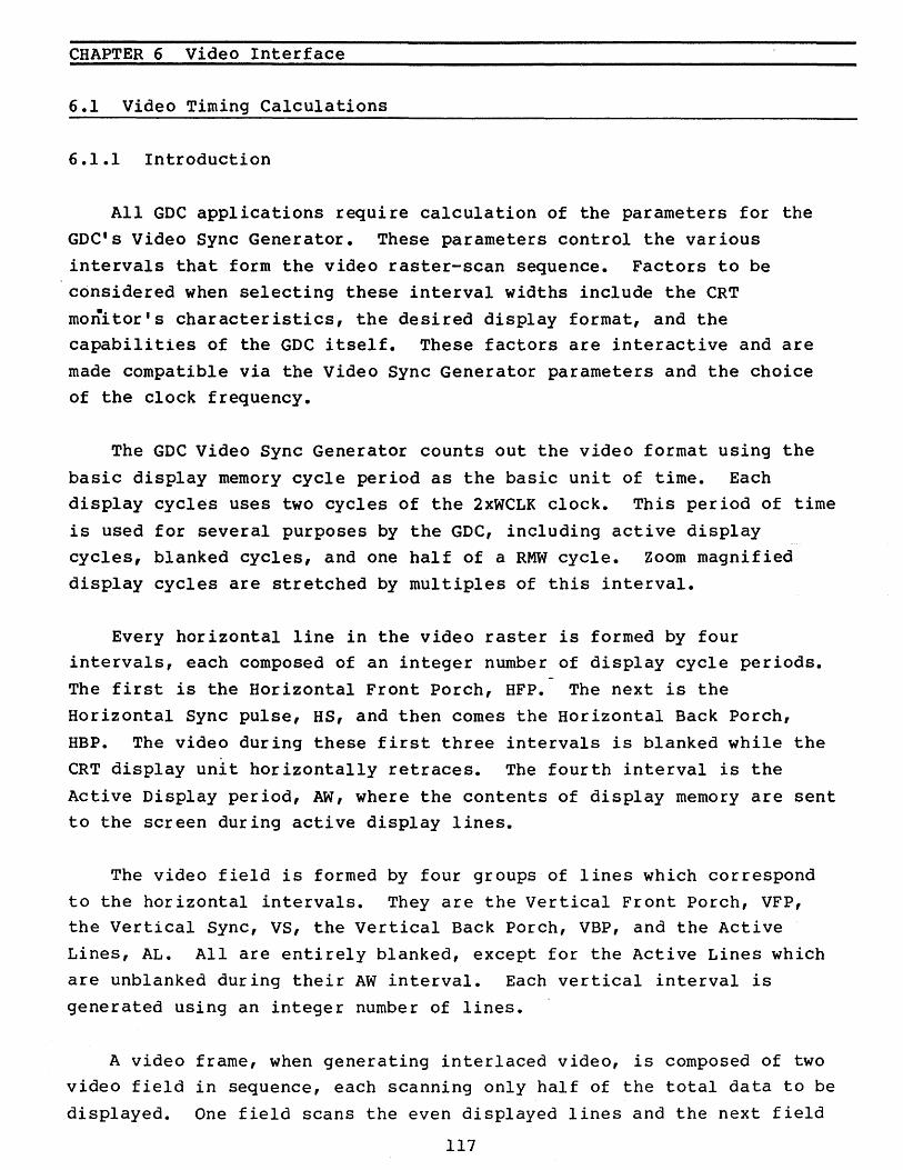
CHAPTER 6 Video Interface
6.1 Video Timing Calculations
6.1.1 Introduction
All GDC applications require calculation of the parameters for the GDC's Video Sync Generator. These parameters control the various
intervals that form the video raster-scan sequence. Factors to be considered when selecting these interval widths include the CRT
monitor's characteristics, the desired display format, and the capabilities of the GDC itself. These factors are interactive and are
made compatible via the Video Sync Generator parameters and the choice of the clock frequency.
The GDC Video Sync Generator counts out the video format using the
basic display memory cycle period as the basic unit of time. Each display cycles uses two cycles of the 2xWCLK clock. This period of time
is used for several purposes by the GDC, including active display cycles, blanked cycles, and one half of a RMW cycle. Zoom magnified display cycles are stretched by multiples of this interval.
Every horizontal line in the video raster is formed by four intervals, each composed of an integer number of display cycle periods.
The first is the Horizontal Front Porch, HFP. The next is the Horizontal Sync pulse, HS, and then comes the Horizontal Back Porch,
HBP. The video during these first three intervals is blanked while the CRT display unit horizontally retraces. The fourth interval is the
Active Display period, AW, where the contents of display memory are sent to the screen during active display lines.
The video field is formed by four groups of lines which correspond to the horizontal intervals. They are the Vertical Front Porch, VFP, the Vertical Sync, VS, the Vertical Back Porch, VBP, and the Active
Lines, AL. All are entirely blanked, except for the Active Lines which are unblanked during their AW interval. Each vertical interval is generated using an integer number of lines.
A video frame, when generating interlaced video, is composed of two video field in sequence, each scanning only half of the total data to be displayed. One field scans the even displayed lines and the next field
117
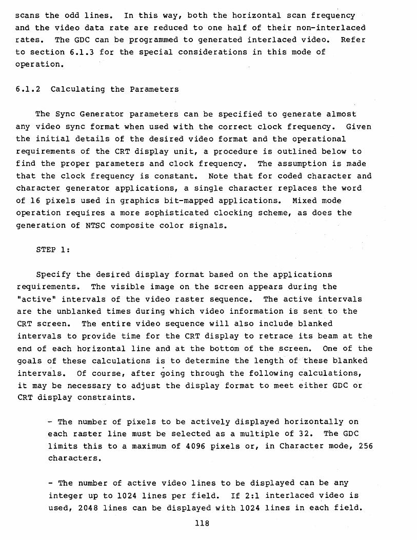
scans the odd lines. In this way, both the horizontal scan frequency and the video data rate are reduced to one half of their non-interlaced rates. The GDC can be programmed to generated interlaced video. Refer to section 6.1.3 for the special considerations in this mode of operation.
6.1.2 Calculating the Parameters
The Sync Generator parameters can be specified to generate almost
any video sync format when used with the correct clock frequency. Given the initial details of the desired video format and the operational requirements of the CRT display unit, a procedure is outlined below to find the proper parameters and clock frequency. The assumption is made
that the clock frequency is constant. Note that for coded character and character generator applications, a single character replaces the word of 16 pixels used in graphics bit-mapped applications. Mixed mode operation requires a more sophisticated clocking scheme, as does the
generation of NTSC composite color signals.
STEP 1:
Specify the desired display format based on the applications requirements. The visible image on the screen appears during the
"active" intervals of the video raster sequence. The active intervals are the unblanked times during which video information is sent to the CRT screen. The entire video sequence will also include blanked intervals to provide time for the CRT display to retrace its beam at the
end of each horizontal line and at the bottom of the screen. One of the goals of these calculations is to determine the length of these blanked . intervals. Of course, after going through the following calculations, it may be necessary to adjust the display format to rneeteither GDC or CRT display constraints.
- The number of pixels to be actively displayed horizontally on each raster line must be selected as a multiple of 32. The GDC limits this to a maximum of 4096 pixels or, in Character mode, 256 characters.
- The number of active video lines to be displayed can be any
integer up to 1024 lines per field. If 2:1 interlaced video is used, 2048 lines can be displayed with 1024 lines in each field.
118
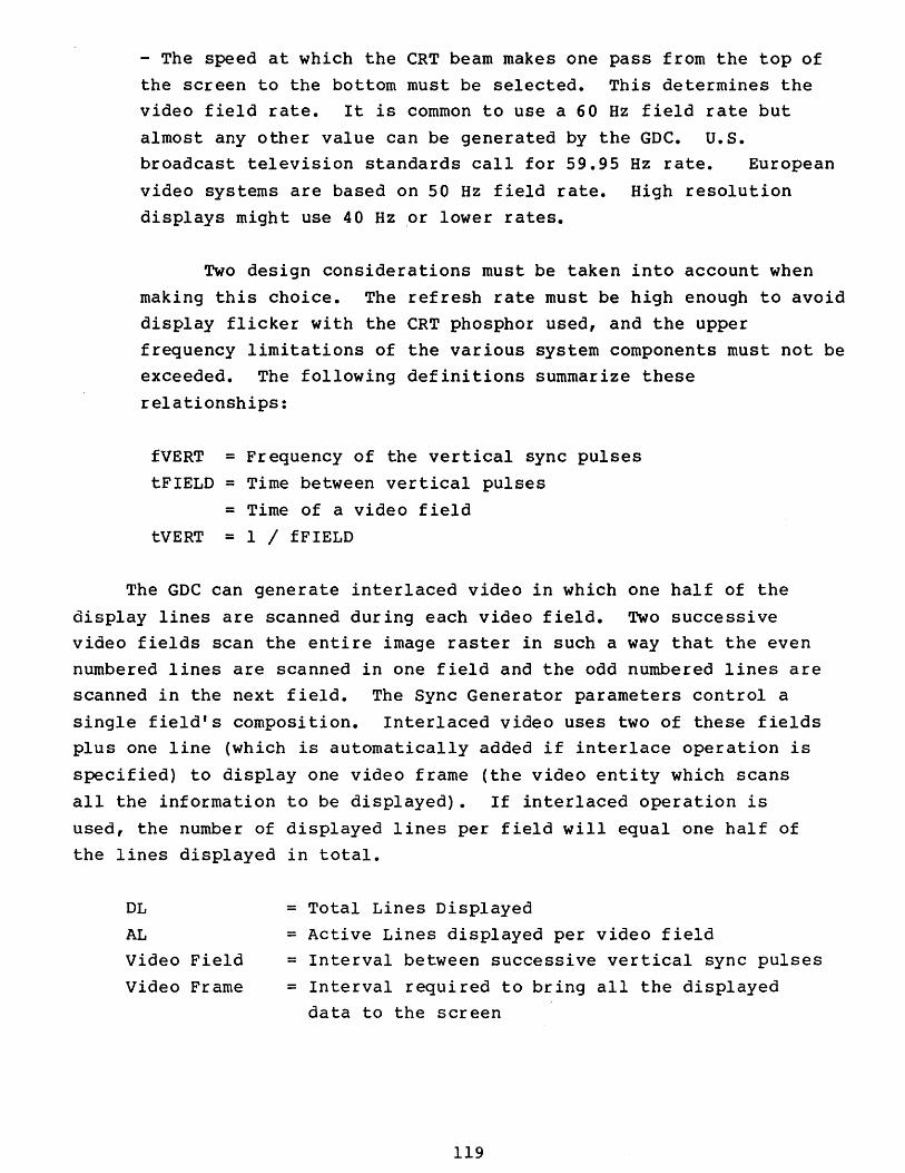
- The speed at which the CRT beam makes one pass from the top of the screen to the bottom must be selected. This determines the video field rate. It is common to use a 60 Hz field rate but
almost any other value can be generated by the GDC. u.s. broadcast television standards call for 59.95 Hz rate. European
video systems are based on 50 Hz field rate. High resolution displays might use 40 Hz ,or lower rates.
Two design considerations must be taken into account when making this choice. The refresh rate must be high enough to avoid display flicker with the CRT phosphor used, and the upper frequency limitations of the various system components must not be exceeded. The following definitions summarize these relationships:
fVERT = Frequency of the vertical sync pulses tFIELD = Time between vertical pulses
= Time of a video field
tVERT = I / fFIELD
The GDC can generate interlaced video in which one half of the
display lines are scanned during each video field. Two successive video fields scan the entire image raster in such a way that the even numbered lines are scanned in one field and the odd numbered lines are scanned in the next field. The Sync Generator parameters control a
single field's composition. Interlaced video uses two of these fields plus one line (which is automatically added if interlace operation is
specified) to display one video frame (the video entity which scans all the information to be displayed). If interlaced operation is
used, the number of displayed lines per field will equal one half of the lines displayed in total.
DL AL Video Field Video Frame
= Total Lines Displayed = Active Lines displayed per video field = Interval between successive vertical sync pulses = Interval required to bring all the displayed
data to the screen
119
For interlaced video (2 fields per frame):
AL = DL / 2
For non-interlaced video:
AL = DL
STEP 2:
The next step is to determine the requirements of the video CRT
unit. The values listed below are important in the calculations establishing the video parameters. The display unit must be capable of displaying the desired video format. It is important during the calculations to check the results against the capabilities of the equipment and devices to find any incompatibilities.
Vertical Blanking Requirement: tVB, min. and max.
(RS-343: 1250 usec + 150 usee = 1100 to 1400 usee)
Horizontal Blanking Requirement: tHB, min and max.
(RS-343: 7 usec + 0.250 usee = 6.75 to 7.25 usee)
Horizontal Sweep Frequency: fHORIZ, min and max.
STEP 3:
The video field must be composed of an integer number of lines.
These lines must be broken down first into the active display lines and the blanked vertical retrace lines. Later the blanked lines will be further divided into the VFP, VS, and VBP intervals. The number of active lines has been specified above as AL. Here the number of blan~ed lines must be determined to provide the CRT enough blanking. The sum of the two line types will be the number of lines in the video field and will be used to calculate the horizontal sweep frequency.
To find the number of lines needed for the vertical blanking period it is necessary to find the maximum time of the active
120
interval. Dividing this by the known number of active lines will give the maximum length line time since the overriding concern is to have
the lowest horizontal frequency consistent with the CRT's requirements. All lines must be of the same length so we can divide the minimum vertical blanking time by this longest line time to find the number of lines needed for blanking. Of course, it is highly unlikely that this will be an even number. Therefore, it will be necessary to round this up to the next larger integer value. This will boost the horizontal sweep frequency slightly above the lowest
possible, but it will assure the proper amount of blanking. Knowing the actual number of lines in the raster will allow the calculation of the exact line time in the next step.
In some situations the total number of lines in the raster, blanked and unblanked, will be given. In this case, the line time will be easy to calculate without the preliminaries described above.
Vertical Active Display Time: tVA
tVA tVA (max)
= =
tFIELD - tVB tFIELD - tVB (min)
Time of one horizontal sweep, tLINE (approximate value):
tLINE (approx) = tVA (max) / AL
Number of blanked lines, BL:
BL = tVB(min) / tLINE (approx) <round up>
Number of total lines in the video field raster, TL:
TL = AL + BL
121
STEP 4:
Once the total number of lines in the video field, TL, is determined, the time of a horizontal sweep can be easily calculated using the duration of the video field, tFIELD, which was determined in Step 3. The horizontal sweep frequency can then be calculated and
compared to the capabilities of the CRT unit.
The actual horizontal sweep period, tLINE:
tLINE = tFIELD / TL
The frequency of the horizontal sweep, fHORIZ:
fHORIZ = 1 / tLINE
STEP 5:
Given the exact line time, tLINE, and the number of blanked lines during vertical retrace, the length of the vertical blanking interval can be calculated and compared with the CRT unit's requirements.
The actual time of the vertical blanking interval:
tVB (actual) = tFIELD - (BL * tLINE)
STEP 6:
Now that the major vertical parameters are established, the variables within the video line can be computed. Like the vertical
format, each horizontal line can be divided into a blanked retrace part and an active part. The horizontal retrace of the CRT beam is
done during the blanked time of each line. The active part of the line is unblanked during active display lines to display the video
data on the CRT screen. During the vertical retrace period, this part , of the line is blanked along with the horizontal retrace period.
The maximum time of the horizontal active period, tAH(max}:
tHA(max} = tLINE - tHB(min}
122
Active words displayed per line, AW:
AW = AP / 16
The approximate time of a display cycle, tOC:
tOC(approx) = tHA(max) / AW
The number of blanked display words per line, BW:
BW = tHB(min) / tOC(approx) <round up>
The total word accesses per line, TW:
TW = AW + BW
The actual time length of each display access cycle, toe:
toc = tLINE / TW
STEP 7:
With the exact length of the basic access cycle time determined, the actual length of the horizontal blanking interval can be computed. The calculations above will yield a value that is a fraction of an access cycle time longer than the target length. Of course, another target time could have been used in place of the minimum CRT blanking
requirement if there had been overriding considerations. In either case it is important to find the exact blanking interval time and
compare it to the original requirement. In cases of a very narrow range of acceptable values, it may be difficult to find an integer
number of cycles which will work.
The actual duration of the horizontal blanking interval:
tHB = toC * BW
123
STEPS:
In the normal graphics operating mode of the GDC, a display cycle accesses 16 pixels to send to the CRT. Therefore, the frequency of the pixel clock must be sixteen times the display cycle frequency, fDC, and eight times the frequency of 2xWCLK. This is the mode of operation used throughout this discussion.
Two other modes of operation can be used instead of the normal 16 pixels per word Graphics mode. In the wide display access mode, the pixel clock is 32 times the display cycle frequency (16 times f2xWCLK) so that 32 pixels can be accessed from even and odd word pairs simultaneously. In the Mixed mode, a graphics area uses four 2xWCLK cycles for each active display cycle. Each display cycle accesses 16 pixels in twice as many GDC clock cycles as the normal mode uses. Therefore, the pixel clock frequency is four times f2xWCLK, instead of the normal eight times. The GDC outputs the display address twice for each display word, effectively accessing each location twice, so the AW parameter value must be twice the normal mode'S value for the same
number of displayed pixels. During horizontal retrace, two GDC clocks define a "display cycle" word time as in the normal operating mode. If these modes are used, the Active Words parameter, AW, must be adjusted accordingly for the earlier calculation, as must the
relationships between the various clocks.
The pixel period, tPIX (normal graphics mode):
tPIX = tDC/16
The frequency of the pixel clock, fPIX:
fPIX = I / tPIX
The GDC clock period, t2xWCLK:
t2xWCLK = tDC / 2 (Two 2xWCLK cycles per display cycle)
The frequency of the GDC clock, f2xWCLK:
f2xWCLK = 1/ t2xWCLK
124
Be sure to compare f2xWCLK to'the GDC's upper and lower clock frequency limits. Proper operation of the device cannot be guaranteed outside these limits, even though the device may appear to work under laboratory conditions. If a limit is exceeded, it may be possible to change the mode of operation of the device as described above to move the clock frequency back within the allowed range.
STEP 9:
The horizontal blanked display cycle words, specified by BW, must be broken down into three intervals for the GDC: Horizontal Front
Porch, HFP, Horizontal Sync, HS, and Horizontal Back Porch, HBP. The relationship between them is:
BW = HFP + HS + HBP
where each variable is an integer number of display cycle word periods. These individual values are chosen based on several considerations. First, there are minimum width requirements for these intervals in various operating modes to provide time for the GDC's Command Processor to handle its tasks during horizontal blanking time. Second, if dynamic RAM refresh is enabled for the display memory, Horizontal Sync must be wide enough to provide at least the minimum RAM refresh rate at the horizontal sweep frequency in use. During Horizontal Sync, each display cycle address comes·from an internal refresh counter, if refresh is enabled. These refresh cycles have the highest priority in the GDC's display memory cycle arbitration scheme
to ensure they are never interrupted or delayed. Third, the Horizontal Sync pulse width and position must meet the CRT display unit's requirements. When there is a conflict between these considerations they must be resolved in the order in which they are presented here. External hardware may have to be added in some cases, or the clock to the GDC can be speeded up during retrace time, etc.
125
Horizontal Front Porch, HFP Constraints:
In general
HFP ~ 2 Display Cycles (4 2xWCLK cycles)
If Video Sync Slave mode is used then HFP ~ 4 Display Cycles (8 2xWCLK cycles)
If the Light Pen is used then
HFP ~ 6 Display Cycles (12 2xWCLK cycles)
Horizontal Sync, HS, Constraints:
If DRAM refresh is enabled,
HS ~ 2 Display Cycles (4 2xWCLK cycles)
If Interlaced Display mode is used then HS ~ 3 Display Cycles (6 2xWCLK cycles)
Horizontal Back Porch, HBP Constraints:
In general
HBP ~ 3 Display Cycles (6 2xWCLK cycles)
If the IMAGE or WD modes change in the video field, HBP ~ 5 Display Cycles (10 2xWCLK cycles)
If the Interlace Display and split screen are used,
HBP ~ 5 Display cycles (10 2xWCLK cycles)
The dynamic RAM refresh rate must be set just fast enough to meet
the requirements of the RAMs and to provide as much drawing time during the horizontal line as possible. Considering uPD4164-type 64K
RAMs, 128 refresh cycles must be done every 2000 usec. Since refresh cycles are done only Quring the Horizontal Sync (HSYNC) interval of
each line, each video line must do enough refresh cycles so that in 2000 usec, 128 cycles have been executed. Other RAMs might require a
different number of refresh cycles in a different time period.
The variables of concern are:
- The Refresh Interval, tREFRESH (2000 usec for 4l64s) - The Refresh Cycle Count, RCC (128 for 4164s)
- The time of a horizontal sweep, tLINE
126
The number of video sweep lines per refresh interval, LRI:
LRI = tREFRESH / tLINE <round down>
The minimum number of refresh cycles per line, RCL:
RCL (min) = RCC / LRI <round up>
The number of display cycles in Horizontal Sync, HS:
HS ~ RCL (min)
STEP 10:
Like the horizontal retrace interval, the vertical retrace
interval must also be separated into three parts. Unlike the horizontal retrace interval, there are no restrictions on the number of lines in each interval except that each must be at least one line long. The three interval line counts must total the number of total blanked retrace lines calculated above:
BL = VSP + VS + VBP
where
BL is the number of lines in vertical blanking interval VFP is the number of lines in the Vertical Front Porch VS is the number of lines in the vertical Sync pulse VBP is the number of lines in the Vertical Back Porch
As a point of comparison, television broadcast standards require
VFP = 3, VS = 3, and VBP = BL - VFP - VS. (VFP and the first 3 lines of VBP are used for equalization pulses.)
Here are the crystal frequency and sync parameters for one particular monitor.
127
6.1.2.1 NEC CU-2002P2 Monitor Timing Calculations
Basic monitor timing specifications:
Horizontal Frequency = 22.7 kHz = 44.053 usec = H Vertical Frequency = 43 to 50.7 Hz, use 50 Hz = 20,000 HBlanking = 9.0 usec min, 12 usec typ VBlanking = 1000 usec min, 2112 usec typ HFP = 4 usec typ HSYNC = 2 usec typ HBP = 6 usec typ VFP = 528 usec typ (12 H) VS = 528 usec typ (12 H) VBP = 1,056 usec typ (24 H)
tACTIVE = 32 usec typ
Number of sweeps in one field (use 50 HZ):
22.7 kHz 50 Hz
sweeps/sec fields/sec
= 454 sweeps/field
Number of sweeps during VBlanking = 12 + 12 + 24 = 48 lines
Number of active lines = 454 - 48 = 406 lines For a 4:3 aspect ratio:
406 lines * 4/3 Pixels = 539.98 Lines
The GDC must have an even multiple of 16 pixels Active:
539.98/16 = 33.75 words
usec
The GDC can generate 32 or 34 words for 512 pixels or 544 pixels.
Use 544 pixels by 406 lines for A.R. = 544 = 1.34 406
Determine the number of word times per line:
tACTIVE (typ) = 32 usee
128
two = 32 usee 34 words
tHBLANK (typ) = two (approx.)
= 941.1764 nsee (approx.)
12 usee .941 usee
= 12.75 words
which is rounded up to 13 words
~OS/Line Total = 34 Active + 13 blanked = 47 words
two = 44.053 usee 47
= 937.294 nsee = H
(tHBLANK = 13 H = 12.185 usee)
t2xWCLK = (1/2) two = 468.6 nsee
tpIXEL = (1/8) t2xWCLK = 58.6 nsee
fpIXEL = 17.070439 MHz <-- XTAL OSC
f2xWCLK = 2.1338 MHz
Horizontal Blanking Interval:
13 Wds HB1anking = HFP + HS + HBP
two = 937.3 usee -4usee -6usee
HFP --) 4usee/two = 4.267 wds --) 4 wds. HS --) 2usec/two = 2.13 wds --) 3 wds. HBP --) 6usec:/two = 6.40 wds --) 6 wds.
Vertical Blanking Interval:
VBLANK = 48 lines = VFP + vs
= 3.75
= 2.81
= 5.62
+ VBP
usee usee usee
-12 lines -12 lines -24 lines
129
VFP = 12 Lines VS = 12 Lines
VBP = 24 Lines
6.1.2.2 Video Format Check
XTAL asc frequency = 17.070439 mHz
Number of words per line = 47 words per line Number of lines per field = 454 sweeps per line
two = 16 = 937.2928 nsec 17.070439 mHz
tLINE = 47 two = 44.052761 usec --) 22.7 kHz
tFIELO = 454 tLINE = 19999.953 usec --) 50 Hz
tHBLANK = 13 two = 12.18 usec
~BLANK = 48 tLINE = 2114.5 usec
HFP = 4 two = 3.749 usec HS = 3 ~O = 2.812 usec HBP = 6 two = 5.624 usec
6.1.3 Special Considerations for Interlaced Video
Interlaced video (2:1 interlaced) is generated using a two-video
field sequence, in which the total line count for both fields is odd, and the vertical sync pulse between the two fields is offset by
exactly one half line time. These conditions,cause the display lines of the second field to be displayed between the lines of the first
field. In this way, an image can be displayed without flicker, at a reduced bandwidth. Interlacing is particularly suited to the display , of camera-(or computer-) generated images (as differentiated from line drawings and text) because of the spatially band-limited nature of
these images. This band-limiting exists along both the horizontal
130
sweep line and vertically across the video lines. Interlaced video is less well suited to typical computer-generated graphics and text displays in that there is no spatial band-limiting in the vertical
direction. For example, one line in the video raster might be black while the very next line is full white. If these lines are scanned in alternate video fields as they are in using interlaced video, there will be very noticeable flicker and apparent vibration. Long persistence phosphors can be used to minimize the problem.
The GDC can be programmed to generate interlaced video. The separate horizontal and vertical sync signals can be used with any CRT
unit which accepts separate sync signals. The total line count of
both fields, one video frame, will be one more than twice the line
count per field for which the GDC is programmed. The GDC's Video Sync Generator adds this extra line automatically and offsets-the second VSYNC pulse by approximately one half line. In typical applications, the second field will be displayed within 15% of the ideal position between the lines of the first field.
Transitions of the VSYNC output during interlaced operation take place at two different pOints with respect to the HSYNC pulse. First
field transitions (both leading and falling edges) occur
simultaneously with the leading edge of BLANK. In the second field, the transitions occur three 2xWCLK cycles before the middle of the active words interval, AW. It does not automatically position the
VSYNC transitions at the exact midpoint of the line including the retrace blanking period. The exact relationship is best shown in the following example.
I HFP I HSYNC I HBP I
First Field VSYNC
~
I I HFP I HSYNC I
==x~ ____________________________ ~x~ ________ _
Second Field VSYNC
______________________ ~x~ __________ ~--------
.I. In',,"" B .1 I. Interval A
Figure 6.1 Horizontal Timing Relative to Vertical Sync Transitions
131
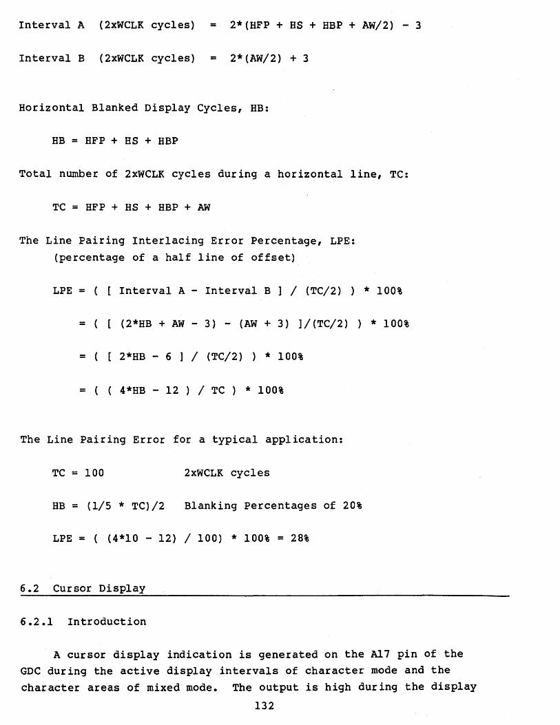
Interval A (2xWCLK cycles) = 2* (HFP + HS + HBP + AW/2) - 3
Interval B (2xWCLK cycles) = 2* (AW/2) + 3
Horizontal Blanked Display Cycles, HB:
HB = HFP + HS + HBP
Total number of 2xWCLK cycles during a horizontal line, TC:
TC = HFP + HS + HBP + AW
The Line pairing Interlacing Error Percentage, LPE:
(percentage of a half line of offset)
LPE = Interval A - Interval B ] / (TC/2) ) * 100%
= ( (2*HB + AW - 3) - (AW + 3) ]/(TC/2) ) * 100%
= [2*HB - 6 ] / (TC/2) ) * 100%
= ( ( 4*HB - 12 ) / TC ) * 100%
The Line pairing Error for a typical application:
TC = 100 2xWCLK cycles
HB = (1/5 * TC)/2 Blanking percentages of 20%
LPE = ( (4*10 - 12) / 100) * 100% = 28%
6.2 Cursor Display
6.2.1 Introduction
A cursor display indication is generated on the AI7 pin of the GDC during the active display intervals of character mode and the character areas of mixed mode. The output is high during the display
132
access time of the word pointed to by the EAD word address of the cursor. This signal can then be used by the external video circuitry to indicate the cursor on the screen with reverse video, a blinking
underline, etc.
6.1.2 Wide Display Mode
The operation of the cursor becomes more involved when the wide display access mode is used. In this situation, the GDC is incrementing the Display Address, DAD, by two for each display cycle. The cursor indication during the display of coded characters must take
this into account. The GDC outputs the cursor display indication in the appropriate half of the display cycle in which the character is accessed.
If the starting address, SAD, of the display area partition is h . ~. even, t e GDC w~ll generate only even addresses as ~t advances by two
addresses for each display cycle. The first half of the display cycle outputs the cursor display status of the first character to be
serialized, which in this case is an even address character. Of course, the GDC expects the external video hardware simultaneously to
access the character at the next higher odd address. The signal level of the cursor pin during the second half of the d~splay cycle indicates the cursor status of this character, which occupies the next higher odd address.
Note that the video hardware is assumed to display the even address character first, and then the odd address character at the next higher address in display memory. The second principle is that the cursor indication for a given character is output one display cycle before the half cycle in which the character will be displayed. If the cursor signal is shifted through two bits of delay, clocked by 2xWCLK rising edges, the resulting cursor signal will line up with the display time of the character.
If the starting address of the display area is odd, the first display cycle will use the odd address as the DAD to the display
memory, but the GDC assumes that the video shift registers still serialize the characters in the even-address-then-odd-address manner. In other words, the second half of the display cycle still corresponds to the odd address character. The difference is that the GDC will be
133
generating the address of the odd address character of the pair. The least significant bit of the display cycle address should be ignored when generating video.
6.2.3 Cursor Programming Considerations
For proper display of other than a block cursor (cursor is the entire row height), the cursor should not be programmed to display on the bottom line of the character row. Under some conditions when the cursor is in the top character row, the CTOP parameter is assumed to be 0 instead of the programmed value, so that the cursor will be displayed from the top line of the character row to the CBOT line.
The CTOP parameter is correctly used in the other character rows.
For interlaced video operation, all the parameter bytes must be given during initialization regardless of operating mode. This is
true for graphics, mixed, and character modes. For non-interlaced operation in graphics mode, only the first parameter byte need be sent
to the GDC.
134
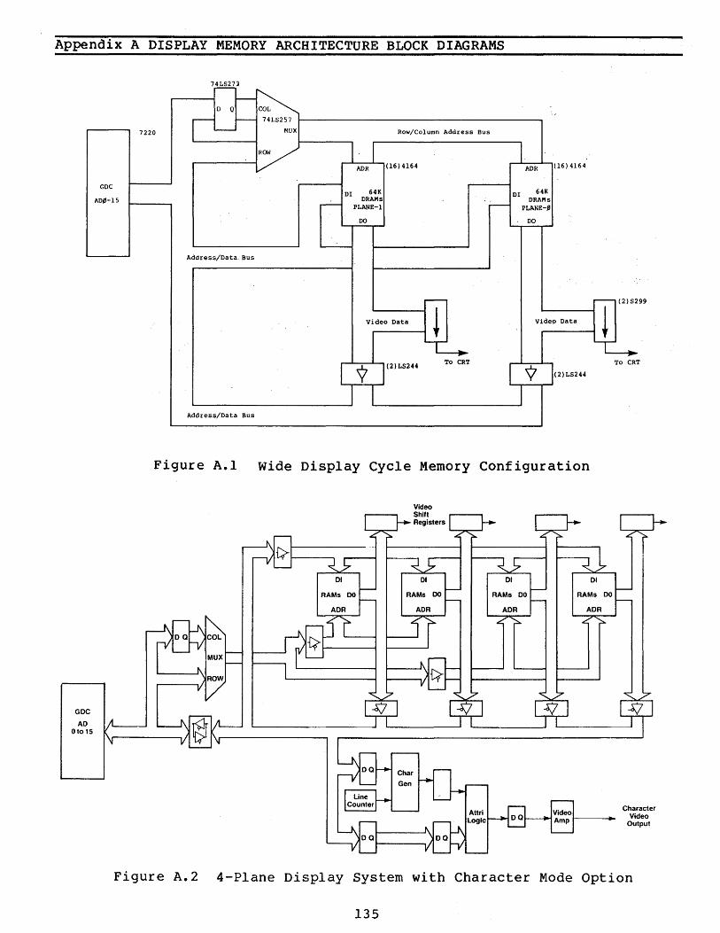
Appendix A DISPLAY MEMORY ARCHITECTURE BLOCK DIAGRAMS
74LS271 -D 0 -~
I~~ 74LS257
7220 MUX Row/Column Address Bus
V ADR (16) 4164 ADR (16) 4164
GDC 64K 64K DI DI
ADJ'-15 .--:- DRAMs ~
DRAMs PLANE-l PLANE-.Il
DO DO
~
Address/Data Bus
r---
Video Data ~ Vide!) Oata
To CRT
? (2)LS244
? (2)LS244
Address/Data Bus
Figure A.l Wide Display Cycle Memory Configuration
GDC
AD Oto15
~(2)S2 99
! To CR T
Character Video
Output
Figure A.2 4-Plane Display System with Character Mode Option
135
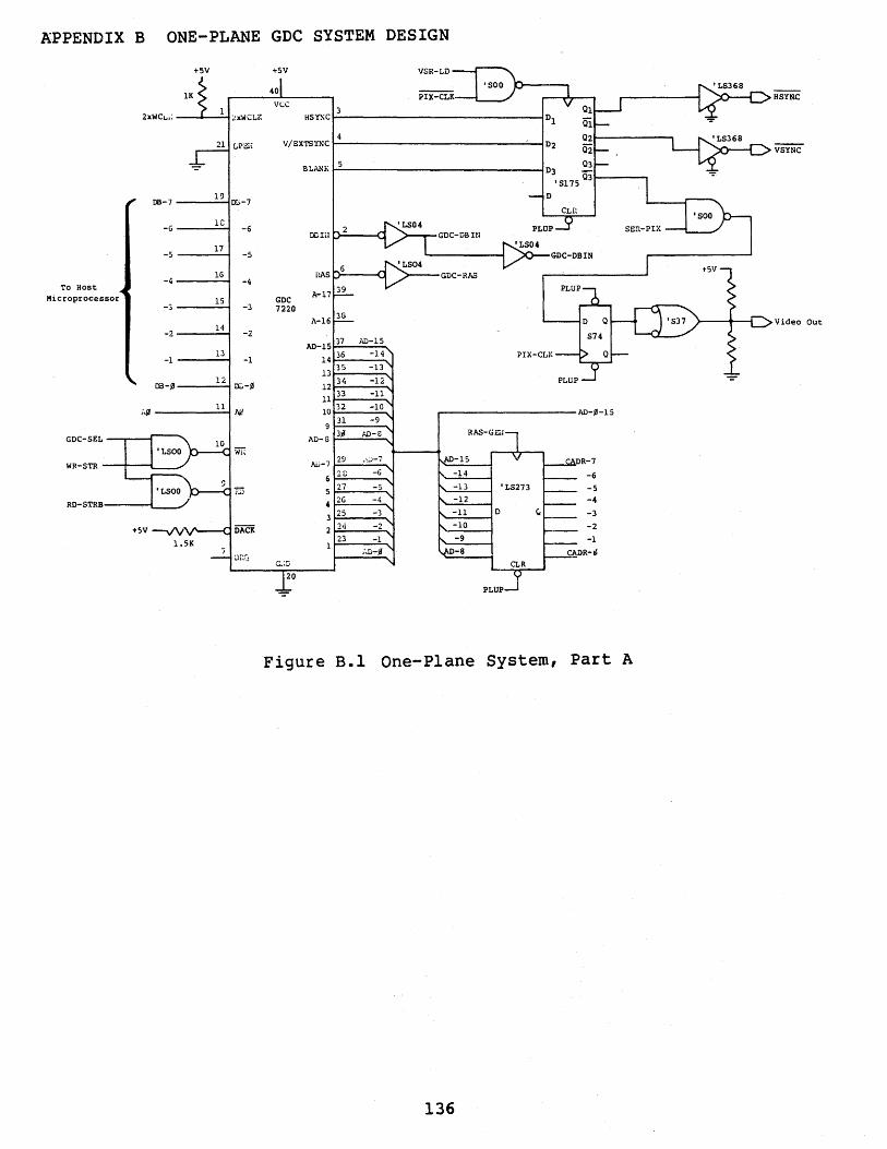
APPENDIX B ONE-PLANE GDC SYSTEM DESIGN
i-5V i-5V VSR-LD
lK HSYNC V~C
2xWCl...: ~xWCLK HSYXC r-------------------------------~Dl
21 LPEli V/EXTSYNC r-----------------------------~~D2
~------------------------------JD3 --• SI 75 03 \------.
-::- BLANK
08-7 19
0'.;-7
-6 Ie
-6 2 ~I,I
-5 17
-5
-4 16 nAS
-4 To Host 39
Microprocessor 15 GDC A-17
-3 -3 7220
A-16 3G
14 -2 -2
Video Out
AD-IS 37 AD-15
13 36 -14 -1 -1 14
PIX-CLK
13 35 -13
03-.0 12
01:.-.0 34 -12
12
11 33 -11
' .. Il 11
N/ 32 -10
10 31 -9
r----------------- AD-.0-IS
GDC-SEL 3j AD-!)
AO-G RAS-GElI
Wl~
WR-STR lUJ-"i 29 .0-7 AD-IS
2(; -6 -14 -6
i=:5 27 -5 -5
RD-STRB 26 -4 -4
25 -3 -3
DACi 24 -2 -2
l.SK 23 -1 -1
Dt~~, i .. D-1l
G.;r:;
20
-=- PLUP
Figure B.l One-Plane System, Part A
136
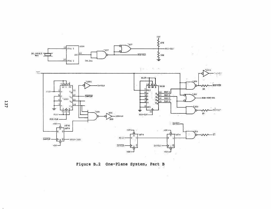
26.181815 MHz
r-----, &224 r-_____ l~S~ i~Ti~L
0::;C~I..;;;2 __ ~
14 '--------t:{'rAL 38.2m:
+5V
270
)----------+--PI:(-CLI;
~-~~--------PIX-CLl: 330
. [.~-"r------------------------------------------~-----------------------.,
LD [l CO
pr,uP D Qo 11
12 I.!c
• 3163 13 I...!i.,j
t~ l1 l \ 14
PLU i' --+--f--J
PIX-CLK
2xllCLI<
'2Xii'C'LK
Figure B.2
PLUP
A
SRI
11 PIX-CLK
VSR+LD
12 nl\S-1
.OD 13 RAS-2
JOc 14 RAS-3 :°8 15 RJ,s-4 OA
2;;I!CLI:
One-Plane System, Part B
RCM-I\OR;-SEL
__ I,,,,,,--Ci\i...~-~ i,; ..
__ ,,,,,,,,--i;T:
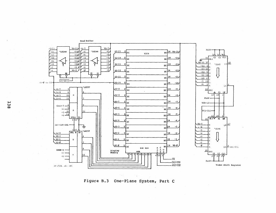
f-J W CO
Read Buffer
.~ ~ iJJ-7 ~ r;-• LS244 ~ ~ =~
• LS244 ~ V_D ~ ~ V:"i2
Y --=!.b V":4
~ ~ ~ v-:-;-
~ -=.!l/ ~ ~ ~ ~ V"7- V":::l
~ ~ ~ r:;-I VD~8 I ~ v-'--
Ell 0; U<
'--- ? ? 9 Y CJe-Do Ili-.J
15
'LS257 .·~-7 3
..... 'u-G 6 4
/\u-5 10 D
,,::.iJ-·4 13 7
r---CI\\)il-7 -2. 9
-G --1. A
-5 .-!.!. 1:<
.,.,:....li . sew Ell
1 15 <:
;;O::-';DP.-SCL -~
1 15 ( I LS257
;.iJ-) SEL B m , .
AD-2 4 i /\ll-1 fi
,Au-II ~ ,.---
9 CAOR-3 - r---
-2-1\ ~ -1-
-i:O'.:!COL ~-.~.\ ;,U:;
Figure B.3
.\0-15 2 00 14 VD-15 01 4164
iJJ-14 2 01
14 -14 00
;'.1)-13 2 01 00
14 -13
111)-12 2 01 00
14 -12
/,0-11 2 01 00
14 -11
AD-I0 2 14 -10 01 00
/ID-9 2 01 00
14 -9
AD-O 2 14 -8 01 00
...;.D-7 2 01
14 -7 00
I\.AO-6 2 14 -6 01 00
~-5 2 01 00
14 -5
lID.,. 4 2 14 -4./ 01 00
AD-) 2 01
14 -:-3 00
\{\D-2 2 01 14 -2
00
lID-I 2 01 00 14 -1
AD-II 2 01 00
14 vo-II R C 641, Rill-i
Display A A 11 ADR .S S E Memory
"'1'1 r 13 'T 11 12
-lIE
Cl\S-GUJ
~
One-Plane System, Part C
PLU?
2 3 9
H Gl C2 CL.:
~ SLI
VD-15 16 J1.. " , S299 t:i: -14 4
G -13 15 ~~
D -12 5 B
-11 14 D
-10 (; (;
-9 13 i:;
-I; 7 i\ ~;J, ~
II Sf:! SI se
12 19 1
PLUP- r--
VSR-LD
PIX-CLK-
12 19 1
~ SLl 51 SfI
VD-7 l! QU rU
I -6 G • S29£i
-5 F
-4
D I::
-) D
-2 C
-:1 L
-[I 1\ ()I" .1:.. ~E:: -PL~
..!!. SHI Gl (;2 eLI:
2 3 9
PLUP
Video Shift Reg ister