Embed Size (px)
Citation preview
1
A 56ndash65 GHz Injection-Locked Frequency Tripler With Quadrature Outputs in 90-nm CMOS
Chan WL Long JRSolid-State Circuits IEEE Journal ofVolume 43 Issue 12 Dec 2008 Page(s)2739 - 2746 Digital Object Identifier 101109JSSC20082004869
學 號 m97662001 學 生 莊明龍 日 期 98 年 03 月 05 日
彰化師範大學積體電路設計研究所
2
Outline
Abstract INTRODUCTION FREQUENCY SYNTHESIS FREQUENCY TRIPLER ARCHITECTURE
AND DESIGN EXPERIMENTIAL RESULTS CONCLUSION
3
Abstract A sub-harmonic injection-locked tripler multipli
es a 20-GHz differential input to 60-GHz quadrature (IQ) output signals
The tripler consists of a two-stage ring oscillator driven by a single-stage polyphase input filter and 50-ohm I and Q-signal output buffers Each gain stage incorporates a hard limiter to triple the input frequency for injection locking and a negative resistance cell with two positive feedback loops to increase gain
4
Abstract (Cont) Regenerative peaking is also used to optimize t
he gainbandwidth performance of the 50-1048576 output buffers Fabricated in 90-nm CMOS the tripler has a free-running frequency of 606 GHz
From a 0-dBm RF source the measured output lock range is 565ndash645 GHz and the measured phase noise penalty is 92 dB with respect to a 202-GHz input The 0303 mm2 tripler (including passives) consumes 96 mW while the output buffers consume 142 mW all from a 1-V supply
5
INTRODUCTION Potential consumer applications include
gigabit per second short-range wireless communication in the 60-GHz and 120-GHz bands long-range collision avoidance radar for automobiles at 77 and 79 GHz and sub-terahertz imaging (94 GHz and above)
Production silicon VLSI technologies have demonstrated a peak transit frequency above 200 GHz for bipolar (NPN) and higher than 300 GHz for CMOS (NFET) which has focused commercial interest towards mm-wave frequency applications for silicon integrated circuits
6
INTRODUCTION (Cont) Implementation of mm-wave transceivers in ba
seline CMOS technology is attractive because of low cost in volume production and RFbaseband co-integration
Single-sideband modulation or demodulation in a mm-wave transceiver requires a mm-wave local oscillator (LO) with quadrature outputs
7
INTRODUCTION (Cont) A phase and amplitude tuning mechanism with
about 5 and 05 dB of correction range is required in order to tune out the unwanted sideband as sideband rejection is often degraded by phase and amplitude errors arising from process voltage and temperature (PVT) variations
An output swing of around 300 mV-pk from the LO source is needed to drive a mm-wave active mixer and the LO output must have adequate spectral purity for the intended application
8
INTRODUCTION (Cont) In this paper a differential CMOS frequency trip
ler with IQ outputs is proposed The circuit is designed around a two-stage injection-locked ring oscillator with tuned LC loads
Sub-harmonic injection-locking occurs when the third harmonic of the input is injected into the LC tank of the oscillator thereby creating an output at three times the input frequency
9
INTRODUCTION (Cont) The quality factorQ of the LC tank loading eac
h ring oscillator stage is decreased by resistive loading to widen the lock range Each gain stage in the ring oscillator uses two positive feedback loops to provide loop gain sufficient to sustain oscillation
10
FREQUENCY SYNTHESIS
Frequency synthesis with PLL
11
FREQUENCY SYNTHESIS (Cont) In a 60-GHz transceiver with zero or low interm
ediate frequency baseband processing the LO operates very close to the received radio-frequency placing the LO in the 60-GHz band
At such high frequencies the phase noise performance of a mm-wave VCO may be adversely affected by tank quality factor layout parasitics and power consumption constraints
12
FREQUENCY SYNTHESIS (Cont) Moreover the local oscillator usually needs to d
rive high-speed dividers in the PLL Frequency divider stages become more difficult to implement and are power hungry at mm-wave frequencies which increases the total power consumption of the receiver
13
FREQUENCY SYNTHESIS (Cont) Frequency synthesis with frequency multipler i
n single conversion
14
FREQUENCY SYNTHESIS (Cont) Frequency synthesis with multiplier in a dual
conversion front-end architecture
15
FREQUENCY SYNTHESIS (Cont) In the homodyne or low-IF topologies the
LO drives the multiplier to generate an output signal N times larger that is used for RF down-conversion The LO frequency may be reduced if more than one stage of down-conversion is used as in a heterodyne architecture
The LO frequency is an even smaller fraction of the RF in the heterodyne architecture In both cases where a multiplier is used the LO operates at a lower frequency than the incoming (RF) frequency
16
FREQUENCY SYNTHESIS (Cont) The IC multiplier relies upon harmonic
frequency generation where the harmonic energy necessarily decreases with increasing frequency More amplifying stages are required to provide a given signal swing as the multiplication factor is increased which drives up power consumption
17
FREQUENCY SYNTHESIS (Cont) push-push oscillator
18
FREQUENCY SYNTHESIS (Cont) unbalanced source coupled pairs
19
FREQUENCY SYNTHESIS (Cont) tuned amplifier
20
FREQUENCY SYNTHESIS (Cont) From the above discussion conventional frequ
ency multipliers can consume substantial power and can only provide single-ended or poorly balanced outputs To reduce power consumption a ring oscillator which can be sub-harmonically injection-locked to an input at 13 the oscillatorrsquos free running frequency is preferred
Moreover a two-stage ring oscillator readily produces quadrature signals which are required for advanced modulation and demodulation schemes
21
FREQUENCY TRIPLER ARCHITECTURE amp DESIGN
Block diagram of the proposed tripler
22
FREQUENCY TRIPLER ARCHITECTURE amp DESIGN (Cont)
The gain cell incorporates a negative resistance cell to compensate for resistive losses which helps to sustain oscillation in the overall loop
The third-harmonic being close to the free-running frequency of the ring oscillator injection-locks the two-stage ring oscillator resulting in a tripled output
23
FREQUENCY TRIPLER ARCHITECTURE amp DESIGN (Cont)
The typical process mismatches for both the resistors and capacitors of the polyphase filter (PPF) designed for 20 GHz become less critical as they have relatively large physical dimensions on-chip
Thus higher phase and amplitude accuracies between the quadrature signals can be expected compared to direct synthesis of quadrature signal from a PPF at 60 GHz
24
FREQUENCY TRIPLER ARCHITECTURE amp DESIGN (Cont) A Injection-Locked Oscillators
25
FREQUENCY TRIPLER ARCHITECTURE amp DESIGN (Cont) A Injection-Locked Oscillators
Simplified schematic of an injection-locked oscillator
26
FREQUENCY TRIPLER ARCHITECTURE amp DESIGN (Cont) A Injection-Locked Oscillators To account for modeling inaccuracies and circu
it variations caused by PVT variations it is assumed that the loop gain must be greater than two Thus lowering the Q to widen the lock range necessitates a higher oscillator bias current which decreases the lock range
The transconductance of the transistors is lower in CMOS compared to bipolar technology for a given DC bias current and therefore more current is required to provide the same gain for a given load
27
FREQUENCY TRIPLER ARCHITECTURE amp DESIGN (Cont) B Oscillator Gain Core
Oscillator gain stage with hard limiter
28
FREQUENCY TRIPLER ARCHITECTURE amp DESIGN (Cont) B Oscillator Gain Core (Cont) The tank inductance is 200 pH which is chosen
as large as possible in order to maximize the lock range A varactor could be connected across the tank for fine frequency tuning if desired
High quadrature accuracy can also be expected from the proposed design as the RF output current from the LC tank does not need to be shared between the coupling and switching transistors as in a typical quadrature oscillator where both of their drain terminals are coupled to the LC tank
29
FREQUENCY TRIPLER ARCHITECTURE amp DESIGN (Cont) B Oscillator Gain Core (Cont)
R1 and R2 load the outputs of the previous gain stage which reduces the Q-factor of the two-stage ring oscillator thereby increasing the injection-locking range
The lock range in turn depends on the injected third harmonic signal strength and their gate bias voltage
Class-B biasing of M5 and M6 maximizes the third harmonic signal strength
30
FREQUENCY TRIPLER ARCHITECTURE amp DESIGN (Cont) C Output Driver
Output buffer with transformer feedback
31
FREQUENCY TRIPLER ARCHITECTURE amp DESIGN (Cont) C Output Driver (Cont)
In this design a magnetic coupling factor of 03 is chosen between the primary and secondary coils of the transformer
At mm-wave frequencies single turn coils are used to achieve low inductance A planar transformer is best suited to realize low coupling coefficient as the distance between the coils can easily be changed
32
FREQUENCY TRIPLER ARCHITECTURE amp DESIGN (Cont) C Output Driver (Cont)
Comparison of simulated output buffer gain
33
FREQUENCY TRIPLER ARCHITECTURE amp DESIGN (Cont) D Simulated Response Under I-L
Simulated relative phase change of the tripler output with injection-locking
34
FREQUENCY TRIPLER ARCHITECTURE amp DESIGN (Cont) D Simulated Response Under I-L
input phase imbalance
35
FREQUENCY TRIPLER ARCHITECTURE amp DESIGN (Cont) D Simulated Response Under I-L
input amplitude error
36
EXPERIMENTIAL RESULTS
Photomicrograph of the tripler test chip
37
EXPERIMENTIAL RESULTS (Cont) The 950850 μm2 test chip has an active area of
300300 μm2 including the inductors and transformers
At its default bias setting the tripler consumes 238 mW from a 1-V supply the two oscillator gain cores dissipate 96 mW and the two output buffers dissipate an additional 142 mW Ten samples from the same batch were measured and their free-running oscillation frequencies ranged from 597 to 606 GHz which is close to the simulated value of 596 GHz
38
EXPERIMENTIAL RESULTS (Cont)
Free-running output spectrum centered at 606 GHz
39
EXPERIMENTIAL RESULTS (Cont) Injection-locked spectrum at 606 GHz for 0-dBm
injected signal at 202 GHz
40
EXPERIMENTIAL RESULTS (Cont)
Measured SSB phase noise of the 202-GHz RF input source and tripler output at 606 GHz
41
EXPERIMENTIAL RESULTS (Cont)
Measured upper and lower frequencies under injection-locking and the resulting lock-range versus RF input power
42
EXPERIMENTIAL RESULTS (Cont) At 565 GHz the output power of the tripler is 8
6 dB lower than the -27 dBm peak power at 606 GHz and the phase noise difference at 100-kHz offset is 103 plusmn1dB compared to 92 plusmn1dB dB At 645 GHz the corresponding output power and phase noise differences are 109 dB and 115 plusmn1dB dB respectively
The smaller output power at the edges of the lock range is due to the bandpass nature of both the ring oscillator and the output buffer
43
EXPERIMENTIAL RESULTS (Cont)
MEASURED PERFORMANCE SUMMARY OF TRIPLER
44
CONCLUSION A sub-harmonic I-L IQ tripler is implemented in
a 90-nm technology The results achieved in this work establish the f
easibility of frequency multiplication in CMOS for mm-wave frequency synthesis easing the design requirements for a lower frequency driving source PLL with respect to desired phase noise performance
45
CONCLUSION (Cont) Design can be used in any desired transceiver ar
chitecture and frequency plan and it creates alternatives to fundamental LO signal generation with the potential for lower overall power consumption
As quadrature accuracy and phase noise are not coupled the IQ tripler can be designed to provide high quadrature phase accuracy and its output phase noise tracks the spectral characteristics of the lower-frequency source oscillator with a negligible penalty in phase noise performance
46
THE END
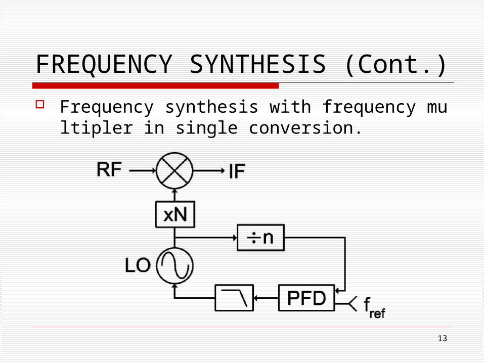
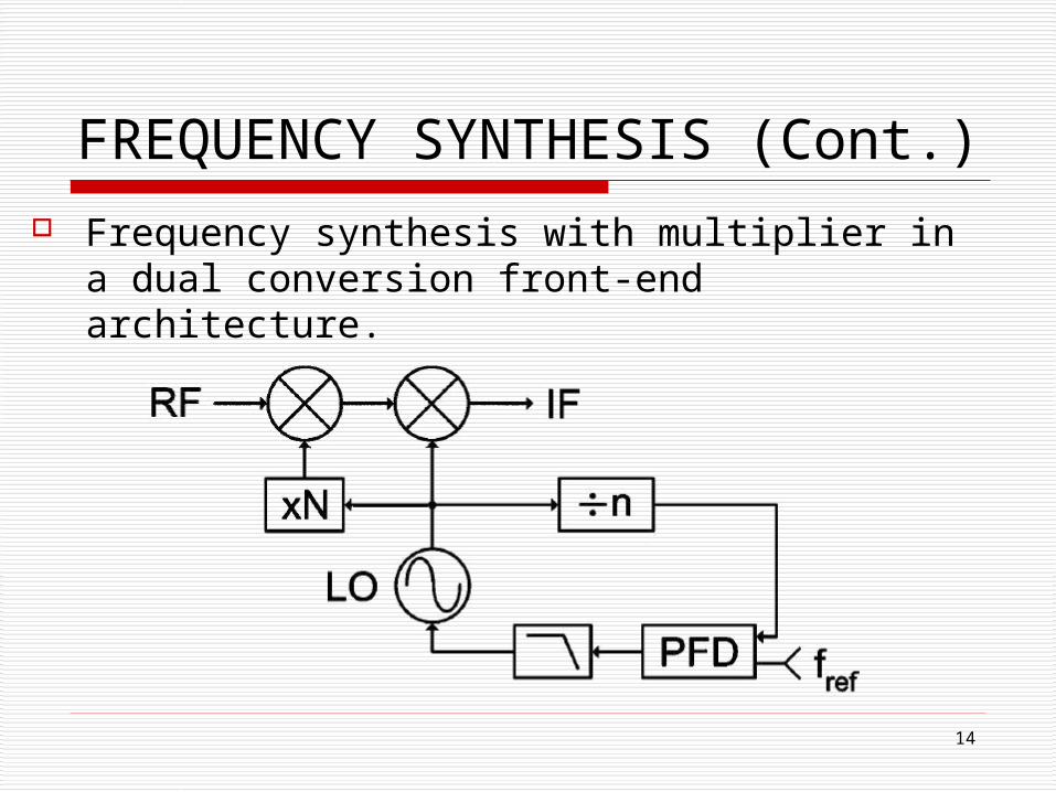
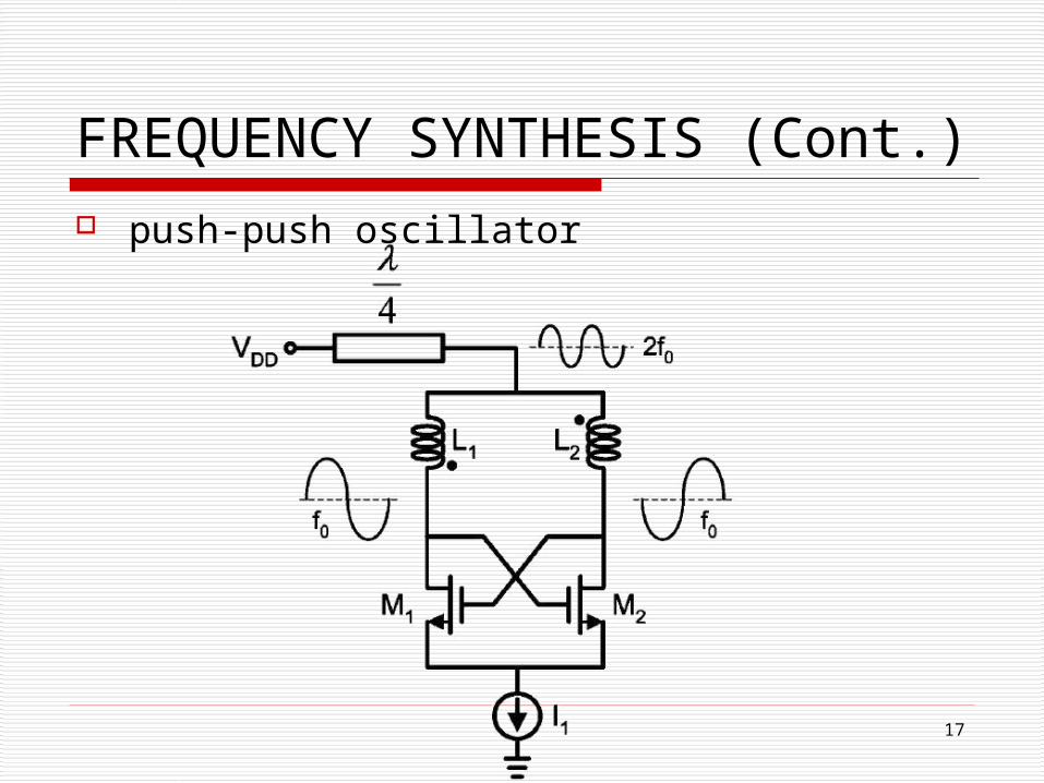
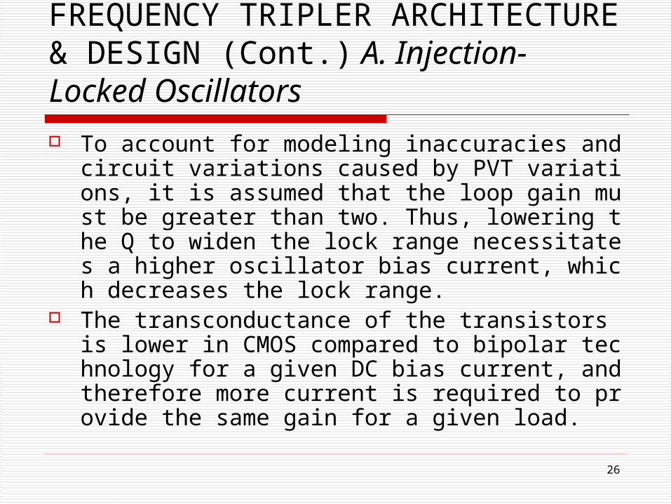

46
THE END