Embed Size (px)
Citation preview
LMR14006
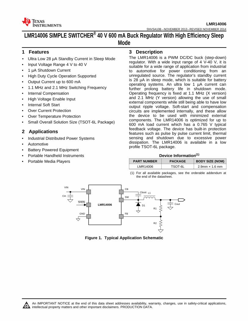
CB
SW
FB
Cboot L1
D1R1
R2
CoutSHDN
VIN
Cin
VIN
GND
LMR14006SNVSA10B –NOVEMBER 2013–REVISED NOVEMBER 2014
LMR14006 SIMPLE SWITCHER® 40 V 600 mA Buck Regulator With High Efficiency SleepMode
1 Features 3 DescriptionThe LMR14006 is a PWM DC/DC buck (step-down)
1• Ultra Low 28 µA Standby Current in Sleep Moderegulator. With a wide input range of 4 V-40 V, it is• Input Voltage Range 4 V to 40 V suitable for a wide range of application from industrial
• 1 µA Shutdown Current to automotive for power conditioning from anunregulated source. The regulator’s standby current• High Duty Cycle Operation Supportedis 28 µA in sleep mode, which is suitable for battery• Output Current up to 600 mA operating systems. An ultra low 1 µA current can
• 1.1 MHz and 2.1 MHz Switching Frequency further prolong battery life in shutdown mode.Operating frequency is fixed at 1.1 MHz (X version)• Internal Compensationand 2.1 MHz (Y version) allowing the use of small• High Voltage Enable Inputexternal components while still being able to have low• Internal Soft Start output ripple voltage. Soft-start and compensation
• Over Current Protection circuits are implemented internally, and these allowthe device to be used with minimized external• Over Temperature Protectioncomponents. The LMR14006 is optimized for up to• Small Overall Solution Size (TSOT-6L Package) 600 mA load current which has a 0.765 V typicalfeedback voltage. The device has built-in protection2 Applications features such as pulse by pulse current limit, thermalsensing and shutdown due to excessive power• Industrial Distributed Power Systemsdissipation. The LMR14006 is available in a low• Automotive profile TSOT-6L package.
• Battery Powered Equipment• Portable Handheld Instruments Device Information(1)
PART NUMBER PACKAGE BODY SIZE (NOM)• Portable Media PlayersLMR14006 TSOT-6L 2.9mm × 1.6 mm
(1) For all available packages, see the orderable addendum atthe end of the datasheet.
Figure 1. Typical Application Schematic
1
An IMPORTANT NOTICE at the end of this data sheet addresses availability, warranty, changes, use in safety-critical applications,intellectual property matters and other important disclaimers. PRODUCTION DATA.

LMR14006SNVSA10B –NOVEMBER 2013–REVISED NOVEMBER 2014 www.ti.com
Table of Contents1 Features .................................................................. 1 7 Detailed Description .............................................. 8
7.1 Overview ................................................................... 82 Applications ........................................................... 17.2 Functional Block Diagram ......................................... 83 Description ............................................................. 17.3 Feature Description................................................... 84 Revision History..................................................... 2
8 Applications and Implementation ...................... 115 Pin Configuration and Functions ......................... 38.1 Typical Applications ................................................ 116 Specifications......................................................... 4
9 Layout ................................................................... 166.1 Absolute Maximum Ratings ...................................... 49.1 Layout Guidelines ................................................... 166.2 Handling Ratings ...................................................... 4
10 Device and Documentation Support ................. 176.3 Recommended Operating Conditions ..................... 410.1 Trademarks ........................................................... 176.4 Thermal Information .................................................. 410.2 Electrostatic Discharge Caution............................ 176.5 Electrical Characteristics........................................... 510.3 Glossary ................................................................ 176.6 Switching Characteristics .......................................... 5
11 Mechanical, Packaging, and Orderable6.7 Typical Characteristics .............................................. 6Information ........................................................... 17
4 Revision HistoryNOTE: Page numbers for previous revisions may differ from page numbers in the current version.
Changes from Original (November 2013) to Revision A Page
• Deleted the other part number LMR14003 from the rest of the document ........................................................................... 1• Added Device Information and Handling Rating tables, Feature Description, Application and Implementation, ,
Layout, Device and Documentation Support, and Mechanical, Packaging, and Orderable Information sections;moved some curves to Application Curves section................................................................................................................ 1
• Changed from 2kV to 1kV ...................................................................................................................................................... 4
Changes from Revision A (September 2014) to Revision B Page
• Changed from -0.3 to -1 ......................................................................................................................................................... 4• Changed from -0.3 to -1 ......................................................................................................................................................... 4
2 Submit Documentation Feedback Copyright © 2013–2014, Texas Instruments Incorporated
Product Folder Links: LMR14006
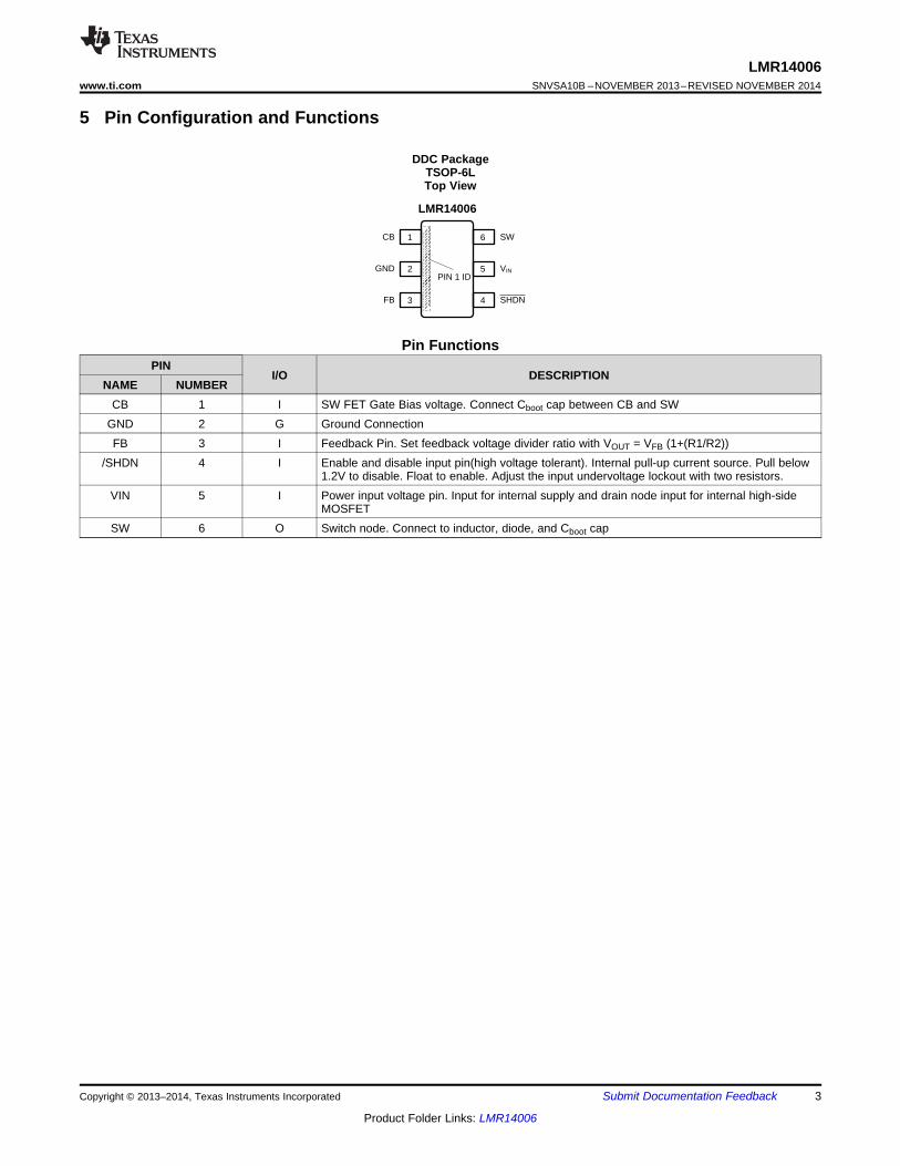
CB 1
2
3 4
5
6
LMR14006
GND
FB
SW
VIN
SHDN
PIN 1 ID
LMR14006www.ti.com SNVSA10B –NOVEMBER 2013–REVISED NOVEMBER 2014
5 Pin Configuration and Functions
DDC PackageTSOP-6LTop View
Pin FunctionsPIN
I/O DESCRIPTIONNAME NUMBER
CB 1 I SW FET Gate Bias voltage. Connect Cboot cap between CB and SWGND 2 G Ground ConnectionFB 3 I Feedback Pin. Set feedback voltage divider ratio with VOUT = VFB (1+(R1/R2))
/SHDN 4 I Enable and disable input pin(high voltage tolerant). Internal pull-up current source. Pull below1.2V to disable. Float to enable. Adjust the input undervoltage lockout with two resistors.
VIN 5 I Power input voltage pin. Input for internal supply and drain node input for internal high-sideMOSFET
SW 6 O Switch node. Connect to inductor, diode, and Cboot cap
Copyright © 2013–2014, Texas Instruments Incorporated Submit Documentation Feedback 3
Product Folder Links: LMR14006
LMR14006SNVSA10B –NOVEMBER 2013–REVISED NOVEMBER 2014 www.ti.com
6 Specifications
6.1 Absolute Maximum Ratingsover operating free-air temperature range (unless otherwise noted) (1)
PARAMETER MIN MAX UNITVIN to GND -0.3 45SHDN to GND -0.3 45
Input Voltages VFB to GND -0.3 7CB to SW -0.3 7SW to GND -1 45
Output Voltages VSW to GND less than 30ns transients -2 45
TJ Operation Junction -40 150 °CTemperature
(1) Stresses beyond those listed under Absolute Maximum Ratings may cause permanent damage to the device. These are stress ratingsonly, which do not imply functional operation of the device at these or any other conditions beyond those indicated under RecommendedOperating Conditions. Exposure to absolute-maximum-rated conditions for extended periods may affect device reliability.
6.2 Handling RatingsMIN MAX UNIT
Tstg Storage temperature range -55 165 °CHuman body model (HBM), per ANSI/ESDA/JEDEC JS-001, all 1000pins except CB pin (1)
V(ESD) Electrostatic discharge VCharged device model (CDM), per JEDEC specification 500JESD22-C101, all pins (2)
(1) JEDEC document JEP155 states that 500-V HBM allows safe manufacturing with a standard ESD control process, CB pin passes 500Vtest.
(2) JEDEC document JEP157 states that 250-V CDM allows safe manufacturing with a standard ESD control process.
6.3 Recommended Operating Conditions (1)
Over operating free-air temperature range (unless otherwise noted)PARAMETER MIN MAX UNITVIN 4 40 VCB 4 46 V
Buck Regulator CB to SW -0.3 6 VSW -1 40FB 0 5.5 V
Control SHDN 0 40 VTemperature Operating junction temperature -40 125 °C
range, TJ
(1) Stresses beyond those listed under Absolute Maximum Ratings may cause permanent damage to the device. These are stress ratingsonly, which do not imply functional operation of the device at these or any other conditions beyond those indicated under RecommendedOperating Conditions. Exposure to absolute-maximum-rated conditions for extended periods may affect device reliability.
6.4 Thermal InformationTHERMAL METRIC (1) TSOT UNIT
(6 PINS)RθJA Junction-to-ambient thermal resistance 102RθJCtop Junction-to-case (top) thermal resistance 36.9 °C/WRθJB Junction-to board characterization parameter 28.4
(1) All numbers apply for packages soldered directly onto a 3" x 3" PC board with 2 oz. copper on 4 layers in still air in accordance toJEDEC standards. Thermal resistance varies greatly with layout, copper thickness, number of layers in PCB, power distribution, numberof thermal vias, board size, ambient temperature, and air flow.
4 Submit Documentation Feedback Copyright © 2013–2014, Texas Instruments Incorporated
Product Folder Links: LMR14006

LMR14006www.ti.com SNVSA10B –NOVEMBER 2013–REVISED NOVEMBER 2014
6.5 Electrical CharacteristicsVIN = /SHDN = 12V, TA = 25°C, unless otherwise specified.SYMBOL PARAMETER CONDITIONS MIN TYP MAX UNITVIN (Input Power Supply)VIN Operating input voltage 4 40 VISHDN Shutdown supply current VEN = 0V 1 3 µAIQ Operating quiescent current no load, VIN = 12V 28 µA
(non- switching)UVLO Undervoltage lockout Rising threshold 4 V
thresholds Falling threshold 3SHDNVSHDN_Thre Rising SHDN Threshold 1.05 1.25 1.38 V
VoltageISHDN_PIN Input current SHDN = 2.3V –4.2 µA
SHDN = 0.9V –1ISHDN_HYS Hysteresis current –3 µAHIGH-SIDE MOSFETRDS_ON On-resistance VIN = 12V, CB to SW = 5.8V 600 mΩVOLTAGE REFERENCE (FB PIN)VFB Feedback voltage 0.747 0.765 0.782 VCURRENT LIMITILIMIT Current limit VIN = 12V, TJ = 25°C 1200 mATHERMAL PERFORMANCETSHDN Thermal shutdown 170 ºC
thresholdTHYS Hysteresis 10 ºC
6.6 Switching CharacteristicsOver operating free-air temperature range (unless otherwise noted)
PARAMETER TEST CONDITIONS MIN TYP MAX UNITSW (SW PIN)
LMR14006X 935 1100 1285fSW Switching frequency kHz
LMR14006Y 1785 2100 2415TON_MIN Minimum turn-on time fSW = 2.1 MHz 95 ns
LMR14006X 96%DMAX Maximum duty cycle
LMR14006Y 97%
Copyright © 2013–2014, Texas Instruments Incorporated Submit Documentation Feedback 5
Product Folder Links: LMR14006
±1.5%
±1.0%
±0.5%
0.0%
0.5%
1.0%
1.5%
0 100 200 300 400 500 600
Out
put
Vol
tage
Cha
nge
Load Current (mA) C003
0.1
1
10
100
4 14 24 34 44
Inpu
t C
urre
nt (
uA)
Input Voltage (V) C001
Sleep
Shutdown
0
10
20
30
40
50
60
70
80
90
100
0.1 1 10 100 1000
Effi
cien
cy (
%)
Output Current (mA) C001
Vout = 3.3V
Vout = 5V
±4%
±3%
±2%
±1%
0%
1%
2%
3%
4%
5 7 9 11 13 15 17 19 21
Out
put
Vol
tage
Cha
nge
Input Voltage (V) C002
40
50
60
70
80
90
100
0.1 1 10 100 1000
Effi
cien
cy (
%)
Output Current (mA) C002
Vin = 15V
Vin = 18V
30
40
50
60
70
80
90
100
0.1 1 10 100 1000
Effi
cien
cy (
%)
Output Current (mA) C003
Vin = 12V
Vin = 15V
LMR14006SNVSA10B –NOVEMBER 2013–REVISED NOVEMBER 2014 www.ti.com
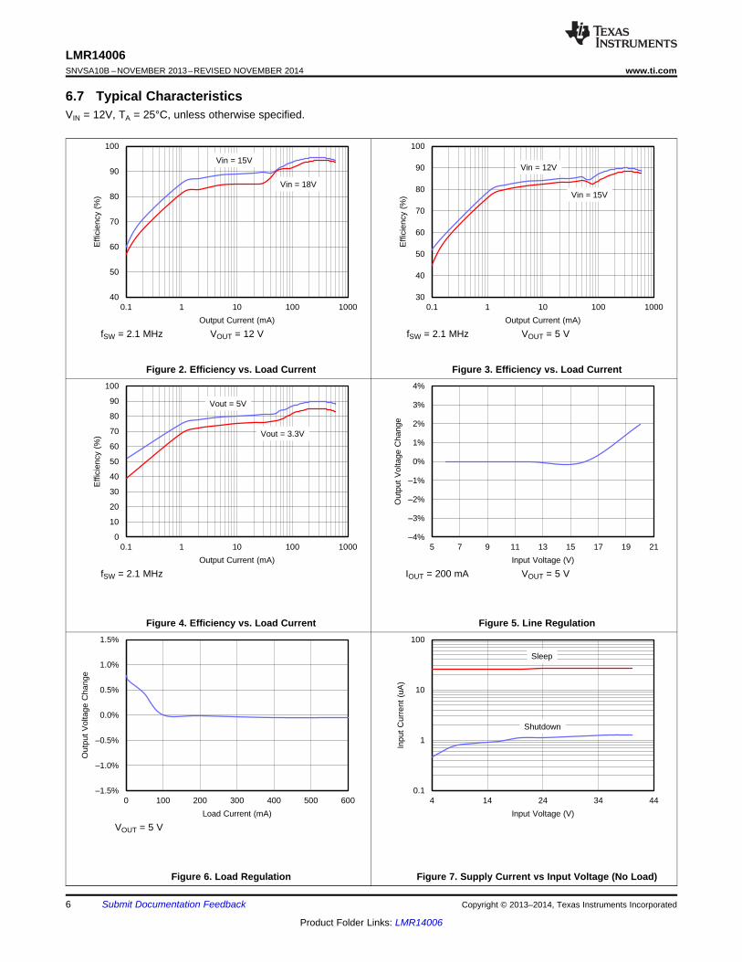
6.7 Typical CharacteristicsVIN = 12V, TA = 25°C, unless otherwise specified.
fSW = 2.1 MHz VOUT = 12 V fSW = 2.1 MHz VOUT = 5 V
Figure 2. Efficiency vs. Load Current Figure 3. Efficiency vs. Load Current
fSW = 2.1 MHz IOUT = 200 mA VOUT = 5 V
Figure 4. Efficiency vs. Load Current Figure 5. Line Regulation
VOUT = 5 V
Figure 6. Load Regulation Figure 7. Supply Current vs Input Voltage (No Load)
6 Submit Documentation Feedback Copyright © 2013–2014, Texas Instruments Incorporated
Product Folder Links: LMR14006
3.10
3.15
3.20
3.25
3.30
3.35
3.40
3.45
3.50
3.55
3.60
±50 0 50 100 150
Und
ervo
ltage
Loc
kout
(V
)
Temperature (C) C004
UVLO_H
UVLO_L
LMR14006www.ti.com SNVSA10B –NOVEMBER 2013–REVISED NOVEMBER 2014
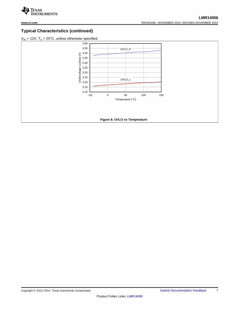
Typical Characteristics (continued)VIN = 12V, TA = 25°C, unless otherwise specified.
Figure 8. UVLO vs Temperature
Copyright © 2013–2014, Texas Instruments Incorporated Submit Documentation Feedback 7
Product Folder Links: LMR14006

GND
SW
CB
VIN
FB
SHDN
HS Driver
EA0.765V
Bootstrap Regulator
Frequency Shift
Bandgap Ref
Main OSC
Logic &PWM Latch
PWM Comparator
+±
Leading Edge Blanking
Slope Compensation
COMPSS
++±
Fixed 5V Option
LMR14006SNVSA10B –NOVEMBER 2013–REVISED NOVEMBER 2014 www.ti.com
7 Detailed Description
7.1 OverviewThe LMR14006 device is a 40 V, 600 mA, step-down (buck) regulator. The buck regulator has a very lowquiescent current during light load to prolong the battery life.
For LMR14006, to improve performance during line and load transients it implements a constant frequency,current mode control which requires less output capacitance and simplifies frequency compensation design. Twoswitching frequency options, 1.1 MHz and 2.1 MHz, are available, thus smaller inductor and capacitor can beused. The LMR14006 reduces the external component count by integrating the boot recharge diode. The biasvoltage for the integrated high side MOSFET is supplied by a capacitor on the CB to SW pin. The boot capacitorvoltage is monitored by an UVLO circuit and will turn the high side MOSFET off when the boot voltage fallsbelow a preset threshold. The LMR14006 can operate at high duty cycles because of the boot UVLO and refreshwimp FET. The output voltage can be stepped down to as low as the 0.8 V reference. Internal soft start isfeatured to minimize inrush currents.
7.2 Functional Block Diagram
7.3 Feature Description
7.3.1 Continuous Conduction ModeThe LMR14006 steps the input voltage down to a lower output voltage. In continuous conduction mode (whenthe inductor current never reaches zero at steady state), the buck regulator operates in two cycles. The powerswitch is connected between VIN and SW. In the first cycle of operation the transistor is closed and the diode isreverse biased. Energy is collected in the inductor and the load current is supplied by Cout and the rising currentthrough the inductor. During the second cycle the transistor is open and the diode is forward biased due to thefact that the inductor current cannot instantaneously change direction. The energy stored in the inductor istransferred to the load and output capacitor. The ratio of these two cycles determines the output voltage. Theoutput voltage is defined approximately as: D = VOUT/VIN and D' = (1-D) where D is the duty cycle of the switch,D and D' will be required for design calculations.
8 Submit Documentation Feedback Copyright © 2013–2014, Texas Instruments Incorporated
Product Folder Links: LMR14006

LMR14006www.ti.com SNVSA10B –NOVEMBER 2013–REVISED NOVEMBER 2014
Feature Description (continued)7.3.2 Fixed Frequency Pwm ControlThe LMR14006 has two fixed frequency options, and it implements peak current mode control. The outputvoltage is compared through external resistors on the VFB pin to an internal voltage reference by an erroramplifier which drives the internal COMP node. An internal oscillator initiates the turn on of the high side powerswitch. The error amplifier output is compared to the high side power switch current. When the power switchcurrent reaches the level set by the internal COMP voltage, the power switch is turned off. The internal COMPnode voltage will increase and decrease as the output current increases and decreases. The device implementsa current limit by clamping the COMP node voltage to a maximum level.
7.3.3 Sleep ModeThe LMR14006 operates in sleep mode at light load currents to improve efficiency by reducing switching andgate drive losses. The LMR14006 is designed so that if the output voltage is within regulation and the peakswitch current at the end of any switching cycle is below the sleep current threshold, IINDUCTOR ≤ 80 mA, thedevice enters sleep mode. For sleep mode operation, the LMR14006 senses peak current, not average or loadcurrent, so the load current where the device enters sleep mode is dependent on the output inductor value.When the load current is low and the output voltage is within regulation, the device enters a sleep mode anddraws only 28 µA input quiescent current.
7.3.4 Bootstrap Voltage (CB)The LMR14006 has an integrated boot regulator, and requires a small ceramic capacitor between the CB andSW pins to provide the gate drive voltage for the high side MOSFET. The CB capacitor is refreshed when thehigh side MOSFET is off and the low side diode conducts. To improve drop out, the LMR14006 is designed tooperate at 100% duty cycle as long as the CB to SW pin voltage is greater than 3 V. When the voltage from CBto SW drops below 3V, the high side MOSFET is turned off using an UVLO circuit which allows the low sidediode to conduct and refresh the charge on the CB capacitor. Since the supply current sourced from the CBcapacitor is low, the high side MOSFET can remain on for more switching cycles than are required to refresh thecapacitor, thus the effective duty cycle of the switching regulator is high. Attention must be taken in maximumduty cycle applications with light load. To ensure SW can be pulled to ground to refresh the CB capacitor, aninternal circuit will charge the CB capacitor when the load is light or the device is working in dropout condition.
7.3.5 Output Voltage SettingThe output voltage is set using the feedback pin and a resistor divider connected to the output as shown inFunctional Block Diagram. The feedback pin voltage 0.765V, so the ratio of the feedback resistors sets theoutput voltage according to the following equation: VOUT = 0.765V (1+(R1/R2)) Typically R2 will be given as 100Ω - 10 kΩ for a starting value. To solve for R1 given R2 and Vout uses R1 = R2 ((VOUT/0.765V)-1).
7.3.6 Enable (/SHDN) and VIN Under Voltage LockoutLMR14006 /SHDN pin is a high voltage tolerant input with an internal pull up circuit. The device can be enabledeven if the /SHDN pin is floating. The regulator can also be turned on using 1.23V or higher logic signals. If theuse of a higher voltage is desired due to system or other constraints, a 100 kΩ or larger resistor is recommendedbetween the applied voltage and the /SHDN pin to protect the device. When /SHDN is pulled down to 0V, thechip is turned off and enters the lowest shutdown current mode. In shutdown mode the supply current will bedecreased to approximately 1 µA. If the shutdown function is not to be used the /SHDN pin may be tied to VIN.The maximum voltage to the SHDN pin should not exceed 40V. LMR14006 has an internal UVLO circuit toshutdown the output if the input voltage falls below an internally fixed UVLO threshold level. This ensures thatthe regulator is not latched into an unknown state during low input voltage conditions. The regulator will power upwhen the input voltage exceeds the voltage level. If there is a requirement for a higher UVLO voltage, the /SHDNcan be used to adjust the input voltage UVLO by using external resistors.
Copyright © 2013–2014, Texas Instruments Incorporated Submit Documentation Feedback 9
Product Folder Links: LMR14006
LMR14006SNVSA10B –NOVEMBER 2013–REVISED NOVEMBER 2014 www.ti.com
Feature Description (continued)7.3.7 Current LimitThe LMR14006 implements current mode control which uses the internal COMP voltage to turn off the high sideMOSFET on a cycle-by-cycle basis. Each cycle the switch current and internal COMP voltage are compared,when the peak switch current intersects the COMP voltage, the high side switch is turned off. During overcurrentconditions that pull the output voltage low, the error amplifier will respond by driving the COMP node high,increasing the switch current. The error amplifier output is clamped internally, which functions as a switch currentlimit.
7.3.8 Overvoltage Transient ProtectionThe LMR14006 incorporates an overvoltage transient protection (OVTP) circuit to minimize voltage overshootwhen recovering from output fault conditions or strong unload transients on power supply designs with low valueoutput capacitance. For example, when the power supply output is overloaded the error amplifier compares theactual output voltage to the internal reference voltage. If the FB pin voltage is lower than the internal referencevoltage for a considerable time, the output of the error amplifier will respond by clamping the error amplifieroutput to a high voltage. Thus, requesting the maximum output current. Once the condition is removed, theregulator output rises and the error amplifier output transitions to the steady state duty cycle. In someapplications, the power supply output voltage can respond faster than the error amplifier output can respond, thisactuality leads to the possibility of an output overshoot. The OVTP feature minimizes the output overshoot, whenusing a low value output capacitor, by implementing a circuit to compare the FB pin voltage to OVTP thresholdwhich is 108% of the internal voltage reference. If the FB pin voltage is greater than the OVTP threshold, thehigh side MOSFET is disabled preventing current from flowing to the output and minimizing output overshoot.When the FB voltage drops lower than the OVTP threshold, the high side MOSFET is allowed to turn on at thenext clock cycle.
7.3.9 Thermal ShutdownThe device implements an internal thermal shutdown to protect itself if the junction temperature exceeds170°C(typ). The thermal shutdown forces the device to stop switching when the junction temperature exceedsthe thermal trip threshold. Once the junction temperature decreases below 160°C(typ), the device reinitiates thepower up sequence.
10 Submit Documentation Feedback Copyright © 2013–2014, Texas Instruments Incorporated
Product Folder Links: LMR14006
LMR14006Y
12V, 0.6A
CB
SW
FB
Cboot100nF
L13.3µH
D1R1
147k
R210k
Cout10µF
SHDN
VIN
Cin2.2µF/50V
VIN
GND
LMR14006Y
5V, 0.6A
CB
SW
FB
Cboot100nF
L110µH
D1R1
54.9k
R210k
Cout10µF
SHDN
VIN
Cin2.2µF/50V
VIN
GND
LMR14006www.ti.com SNVSA10B –NOVEMBER 2013–REVISED NOVEMBER 2014
8 Applications and Implementation
NOTEInformation in the following applications sections is not part of the TI componentspecification, and TI does not warrant its accuracy or completeness. TI’s customers areresponsible for determining suitability of components for their purposes. Customers shouldvalidate and test their design implementation to confirm system functionality.
8.1 Typical Applications
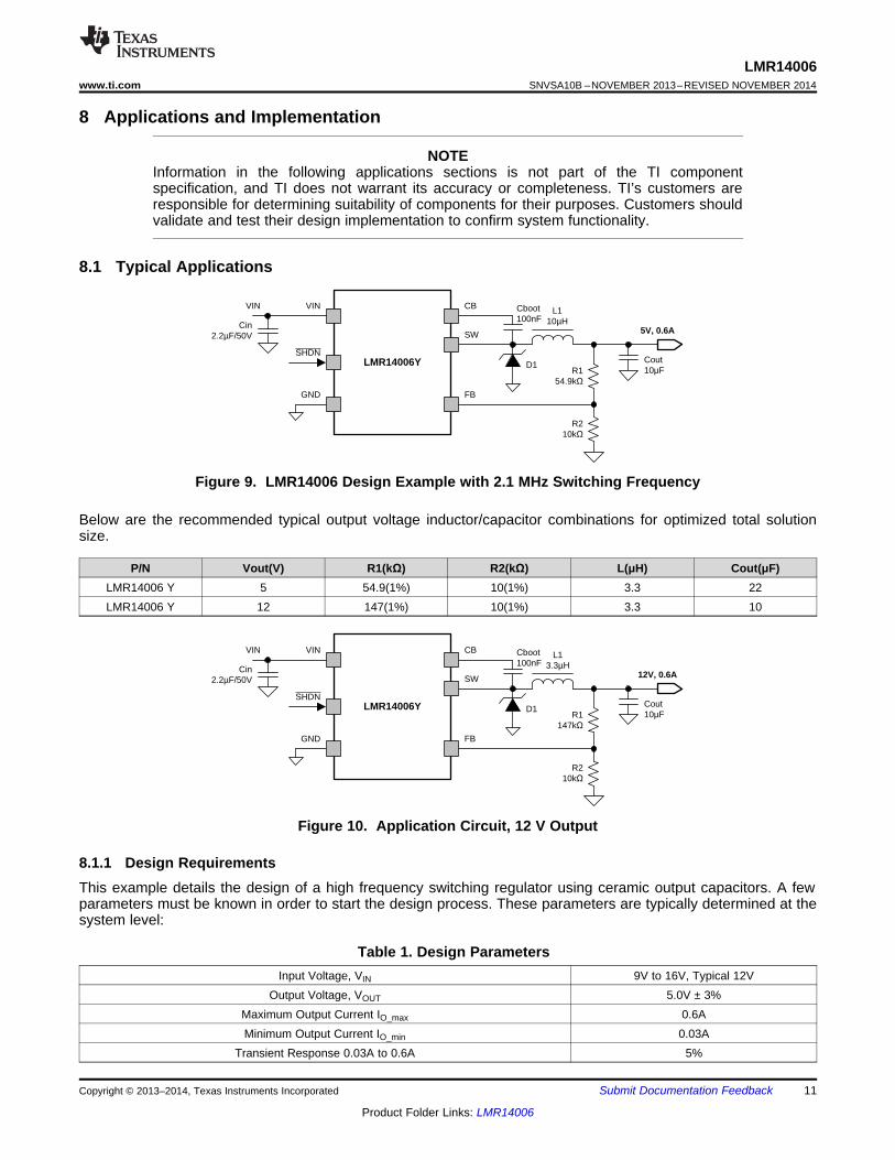
Figure 9. LMR14006 Design Example with 2.1 MHz Switching Frequency
Below are the recommended typical output voltage inductor/capacitor combinations for optimized total solutionsize.
P/N Vout(V) R1(kΩ) R2(kΩ) L(μH) Cout(μF)LMR14006 Y 5 54.9(1%) 10(1%) 3.3 22LMR14006 Y 12 147(1%) 10(1%) 3.3 10
Figure 10. Application Circuit, 12 V Output
8.1.1 Design RequirementsThis example details the design of a high frequency switching regulator using ceramic output capacitors. A fewparameters must be known in order to start the design process. These parameters are typically determined at thesystem level:
Table 1. Design ParametersInput Voltage, VIN 9V to 16V, Typical 12V
Output Voltage, VOUT 5.0V ± 3%Maximum Output Current IO_max 0.6AMinimum Output Current IO_min 0.03A
Transient Response 0.03A to 0.6A 5%
Copyright © 2013–2014, Texas Instruments Incorporated Submit Documentation Feedback 11
Product Folder Links: LMR14006
2
rippleL peak o
II I
2 2112
L-RMS o rippleI I I
max
max
( )u
u u
out in outripple
in o sw
V V VI
V L f
maxmin
max
u
u u
in out outo
o IND in sw
V V VL
I K V f
LMR14006SNVSA10B –NOVEMBER 2013–REVISED NOVEMBER 2014 www.ti.com
Table 1. Design Parameters (continued)Output Voltage Ripple 1%
Switching Frequency Fsw 2.1MHzTarget during Load Transient Over Voltage Peak Value 106% of Output Voltage
Under Voltage Value 91% of Output Voltage
8.1.2 Detailed Design Procedure
8.1.2.1 Selecting The Switching FrequencyThe first step is to decide on a switching frequency for the regulator. Typically, the user will want to choose thehighest switching frequency possible since this will produce the smallest solution size. The high switchingfrequency allows for lower valued inductors and smaller output capacitors compared to a power supply thatswitches at a lower frequency. The switching frequency that can be selected is limited by the minimum on-time ofthe internal power switch, the input voltage and the output voltage and the frequency shift limitation. For thisexample, the output voltage is 5V and the maximum input voltage is 16 V, a switching frequency of 2100 kHz isused.
8.1.2.2 Output Inductor SelectionThe most critical parameters for the inductor are the inductance, peak current and the DC resistance. Theinductance is related to the peak-to-peak inductor ripple current, the input and the output voltages. Since theripple current increases with the input voltage, the maximum input voltage is always used to determine theinductance. To calculate the minimum value of the output inductor, use Equation 1. KIND is a coefficient thatrepresents the amount of inductor ripple current relative to the maximum output current. A reasonable value issetting the ripple current to be 30% of the DC output current. For this design example, the minimum inductorvalue is calculated to be 9.1 µH, and a nearest standard value was chosen: 10 µH. For the output filter inductor,it is important that the RMS current and saturation current ratings not be exceeded. The RMS and peak inductorcurrent can be found from Equation 3 and Equation 4. The inductor ripple current is 0.16 A, and the RMS currentis 0.602 A. As the equation set demonstrates, lower ripple currents will reduce the output voltage ripple of theregulator but will require a larger value of inductance. A good starting point for most applications is a 10 μH with2 A current rating. Using a rating near 2 A will enable the LMR14006 to current limit without saturating theinductor. This is preferable to the LMR14006 going into thermal shutdown mode and the possibility of damagingthe inductor if the output is shorted to ground or other long-term overload.
(1)
(2)
(3)
(4)
8.1.2.3 Output CapacitorThe selection of COUT is mainly driven by three primary considerations. The output capacitor will determine themodulator pole, the output voltage ripple, and how the regulator responds to a large change in load current. Theoutput capacitance needs to be selected based on the most stringent of these three criteria.
12 Submit Documentation Feedback Copyright © 2013–2014, Texas Instruments Incorporated
Product Folder Links: LMR14006
_
_
o rippleESR
L ripple
VR
I
_
_
1 18
! u
uout
o ripple
L ripple
CVfsw
I
2 2
2 2
( )
( )
! u
out o
Ioh IolC L
Vf Vi
2u '!
u '
outout
out
IC
fsw V
LMR14006www.ti.com SNVSA10B –NOVEMBER 2013–REVISED NOVEMBER 2014
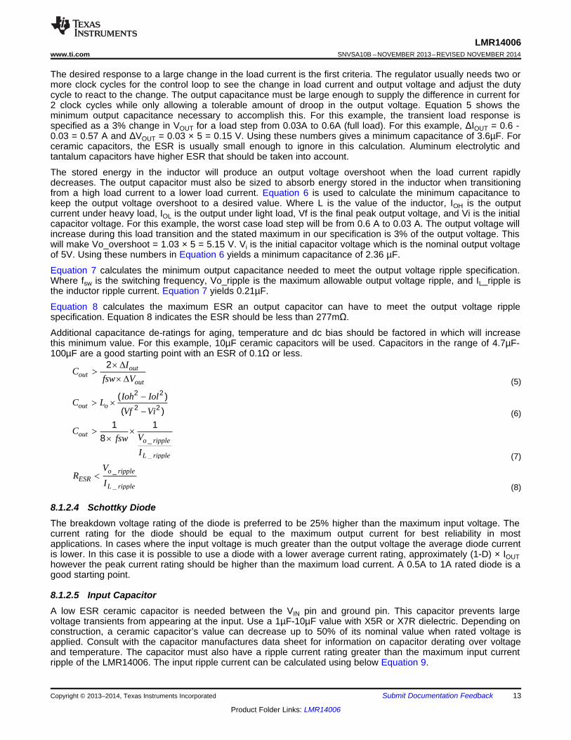
The desired response to a large change in the load current is the first criteria. The regulator usually needs two ormore clock cycles for the control loop to see the change in load current and output voltage and adjust the dutycycle to react to the change. The output capacitance must be large enough to supply the difference in current for2 clock cycles while only allowing a tolerable amount of droop in the output voltage. Equation 5 shows theminimum output capacitance necessary to accomplish this. For this example, the transient load response isspecified as a 3% change in VOUT for a load step from 0.03A to 0.6A (full load). For this example, ΔIOUT = 0.6 -0.03 = 0.57 A and ΔVOUT = 0.03 × 5 = 0.15 V. Using these numbers gives a minimum capacitance of 3.6µF. Forceramic capacitors, the ESR is usually small enough to ignore in this calculation. Aluminum electrolytic andtantalum capacitors have higher ESR that should be taken into account.
The stored energy in the inductor will produce an output voltage overshoot when the load current rapidlydecreases. The output capacitor must also be sized to absorb energy stored in the inductor when transitioningfrom a high load current to a lower load current. Equation 6 is used to calculate the minimum capacitance tokeep the output voltage overshoot to a desired value. Where L is the value of the inductor, IOH is the outputcurrent under heavy load, IOL is the output under light load, Vf is the final peak output voltage, and Vi is the initialcapacitor voltage. For this example, the worst case load step will be from 0.6 A to 0.03 A. The output voltage willincrease during this load transition and the stated maximum in our specification is 3% of the output voltage. Thiswill make Vo_overshoot = 1.03 × 5 = 5.15 V. Vi is the initial capacitor voltage which is the nominal output voltageof 5V. Using these numbers in Equation 6 yields a minimum capacitance of 2.36 µF.
Equation 7 calculates the minimum output capacitance needed to meet the output voltage ripple specification.Where fsw is the switching frequency, Vo_ripple is the maximum allowable output voltage ripple, and IL_ripple isthe inductor ripple current. Equation 7 yields 0.21µF.
Equation 8 calculates the maximum ESR an output capacitor can have to meet the output voltage ripplespecification. Equation 8 indicates the ESR should be less than 277mΩ.
Additional capacitance de-ratings for aging, temperature and dc bias should be factored in which will increasethis minimum value. For this example, 10µF ceramic capacitors will be used. Capacitors in the range of 4.7µF-100µF are a good starting point with an ESR of 0.1Ω or less.
(5)
(6)
(7)
(8)
8.1.2.4 Schottky DiodeThe breakdown voltage rating of the diode is preferred to be 25% higher than the maximum input voltage. Thecurrent rating for the diode should be equal to the maximum output current for best reliability in mostapplications. In cases where the input voltage is much greater than the output voltage the average diode currentis lower. In this case it is possible to use a diode with a lower average current rating, approximately (1-D) × IOUThowever the peak current rating should be higher than the maximum load current. A 0.5A to 1A rated diode is agood starting point.
8.1.2.5 Input CapacitorA low ESR ceramic capacitor is needed between the VIN pin and ground pin. This capacitor prevents largevoltage transients from appearing at the input. Use a 1µF-10µF value with X5R or X7R dielectric. Depending onconstruction, a ceramic capacitor’s value can decrease up to 50% of its nominal value when rated voltage isapplied. Consult with the capacitor manufactures data sheet for information on capacitor derating over voltageand temperature. The capacitor must also have a ripple current rating greater than the maximum input currentripple of the LMR14006. The input ripple current can be calculated using below Equation 9.
Copyright © 2013–2014, Texas Instruments Incorporated Submit Documentation Feedback 13
Product Folder Links: LMR14006

max 0.25u'
u
outin
in
IV
C fsw
min
min min
( )
u uin outout
cirms outin in
V VVI I
V V
LMR14006SNVSA10B –NOVEMBER 2013–REVISED NOVEMBER 2014 www.ti.com
For this example design, one 2.2µF, 50V capacitor is selected. The input capacitance value determines the inputripple voltage of the regulator. The input voltage ripple can be calculated using Equation 10. Using the designexample values, IOUTmax = 0.6A, CIN = 2.2µF, ƒSW = 2100kHz, yields an input voltage ripple of 32.5mV and arms input ripple current of 0.3A.
(9)
(10)
8.1.2.6 Bootstrap Capacitor SelectionA 0.1μF ceramic capacitor or larger is recommended for the bootstrap capacitor (CBOOT). For applications wherethe input voltage is close to output voltage a larger capacitor is recommended, generally 0.1 µF to 1 µF to ensureplenty of gate drive for the internal switches and a consistently low RDSON. A ceramic capacitor with an X7R orX5R grade dielectric with a voltage rating of 10V or higher is recommended because of the stable characteristicsover temperature and voltage.
8.1.3 Application Performance Curves
Vout = 5 V 600 mA Load Vin = 18V 300 mA Load
Figure 11. Switching Node And Output Voltage Waveform Figure 12. 12 V Output Start-Up Waveform
Vin = 18 V 300 mA Load
Figure 13. 12 V Output Shutdown Waveform Figure 14. 5 V Output Start-Up Waveform (300 mA Load)
14 Submit Documentation Feedback Copyright © 2013–2014, Texas Instruments Incorporated
Product Folder Links: LMR14006
LMR14006www.ti.com SNVSA10B –NOVEMBER 2013–REVISED NOVEMBER 2014
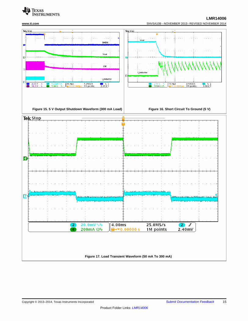
Figure 15. 5 V Output Shutdown Waveform (300 mA Load) Figure 16. Short Circuit To Ground (5 V)
Figure 17. Load Transient Waveform (50 mA To 300 mA)
Copyright © 2013–2014, Texas Instruments Incorporated Submit Documentation Feedback 15
Product Folder Links: LMR14006
LMR14006SNVSA10B –NOVEMBER 2013–REVISED NOVEMBER 2014 www.ti.com
9 Layout
9.1 Layout GuidelinesTo reduce problems with conducted noise pick up the ground side of feedback network should be connecteddirectly to the GND pin with its own connection. The feedback network, resistors R1 and R2, should be keptclose to the FB pin, and away from the inductor to minimize coupling noise into the feedback pin. The inputbypass capacitor CIN must be placed close to the VIN pin. This will reduce copper trace resistance whicheffects input voltage ripple of the IC. The inductor L1 should be placed close to the SW pin to reducemagnetic and electrostatic noise. The output capacitor, COUT should be placed close to the junction of L1 andthe diode D1. The L1, D1, and COUT trace should be as short as possible to reduce conducted and radiatednoise and increase overall efficiency. The ground connection for the diode, CIN, and COUT should be as smallas possible and tied to the system ground plane in only one spot (preferably at the COUT ground point) tominimize conducted noise in the system ground plane. For more detail on switching power supply layoutconsiderations see Application Note AN-1149.
16 Submit Documentation Feedback Copyright © 2013–2014, Texas Instruments Incorporated
Product Folder Links: LMR14006
LMR14006www.ti.com SNVSA10B –NOVEMBER 2013–REVISED NOVEMBER 2014
10 Device and Documentation Support
10.1 TrademarksSIMPLE SWITCHER is a registered trademark of Texas Instruments.All other trademarks are the property of their respective owners.
10.2 Electrostatic Discharge CautionThese devices have limited built-in ESD protection. The leads should be shorted together or the device placed in conductive foamduring storage or handling to prevent electrostatic damage to the MOS gates.
10.3 GlossarySLYZ022 — TI Glossary.
This glossary lists and explains terms, acronyms, and definitions.
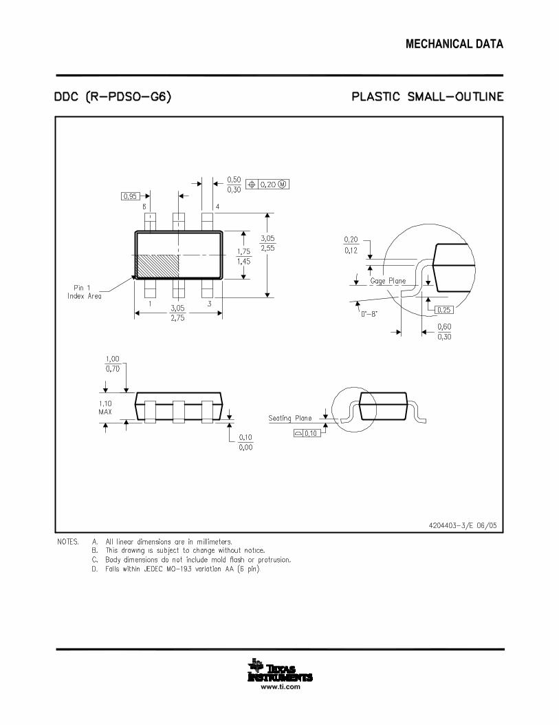
11 Mechanical, Packaging, and Orderable InformationThe following pages include mechanical, packaging, and orderable information. This information is the mostcurrent data available for the designated devices. This data is subject to change without notice and revision ofthis document. For browser-based versions of this data sheet, refer to the left-hand navigation.
Copyright © 2013–2014, Texas Instruments Incorporated Submit Documentation Feedback 17
Product Folder Links: LMR14006
PACKAGE OPTION ADDENDUM
www.ti.com 28-Feb-2017
Addendum-Page 1
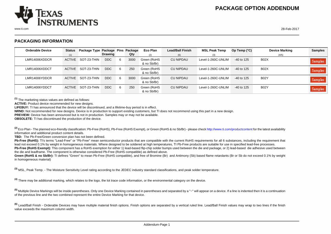
PACKAGING INFORMATION
Orderable Device Status(1)
Package Type PackageDrawing
Pins PackageQty
Eco Plan(2)
Lead/Ball Finish(6)
MSL Peak Temp(3)
Op Temp (°C) Device Marking(4/5)
Samples
LMR14006XDDCR ACTIVE SOT-23-THIN DDC 6 3000 Green (RoHS& no Sb/Br)
CU NIPDAU Level-1-260C-UNLIM -40 to 125 B02X
LMR14006XDDCT ACTIVE SOT-23-THIN DDC 6 250 Green (RoHS& no Sb/Br)
CU NIPDAU Level-1-260C-UNLIM -40 to 125 B02X
LMR14006YDDCR ACTIVE SOT-23-THIN DDC 6 3000 Green (RoHS& no Sb/Br)
CU NIPDAU Level-1-260C-UNLIM -40 to 125 B02Y
LMR14006YDDCT ACTIVE SOT-23-THIN DDC 6 250 Green (RoHS& no Sb/Br)
CU NIPDAU Level-1-260C-UNLIM -40 to 125 B02Y
(1) The marketing status values are defined as follows:ACTIVE: Product device recommended for new designs.LIFEBUY: TI has announced that the device will be discontinued, and a lifetime-buy period is in effect.NRND: Not recommended for new designs. Device is in production to support existing customers, but TI does not recommend using this part in a new design.PREVIEW: Device has been announced but is not in production. Samples may or may not be available.OBSOLETE: TI has discontinued the production of the device.
(2) Eco Plan - The planned eco-friendly classification: Pb-Free (RoHS), Pb-Free (RoHS Exempt), or Green (RoHS & no Sb/Br) - please check http://www.ti.com/productcontent for the latest availabilityinformation and additional product content details.TBD: The Pb-Free/Green conversion plan has not been defined.Pb-Free (RoHS): TI's terms "Lead-Free" or "Pb-Free" mean semiconductor products that are compatible with the current RoHS requirements for all 6 substances, including the requirement thatlead not exceed 0.1% by weight in homogeneous materials. Where designed to be soldered at high temperatures, TI Pb-Free products are suitable for use in specified lead-free processes.Pb-Free (RoHS Exempt): This component has a RoHS exemption for either 1) lead-based flip-chip solder bumps used between the die and package, or 2) lead-based die adhesive used betweenthe die and leadframe. The component is otherwise considered Pb-Free (RoHS compatible) as defined above.Green (RoHS & no Sb/Br): TI defines "Green" to mean Pb-Free (RoHS compatible), and free of Bromine (Br) and Antimony (Sb) based flame retardants (Br or Sb do not exceed 0.1% by weightin homogeneous material)
(3) MSL, Peak Temp. - The Moisture Sensitivity Level rating according to the JEDEC industry standard classifications, and peak solder temperature.
(4) There may be additional marking, which relates to the logo, the lot trace code information, or the environmental category on the device.
(5) Multiple Device Markings will be inside parentheses. Only one Device Marking contained in parentheses and separated by a "~" will appear on a device. If a line is indented then it is a continuationof the previous line and the two combined represent the entire Device Marking for that device.
(6) Lead/Ball Finish - Orderable Devices may have multiple material finish options. Finish options are separated by a vertical ruled line. Lead/Ball Finish values may wrap to two lines if the finishvalue exceeds the maximum column width.
PACKAGE OPTION ADDENDUM
www.ti.com 28-Feb-2017
Addendum-Page 2
Important Information and Disclaimer:The information provided on this page represents TI's knowledge and belief as of the date that it is provided. TI bases its knowledge and belief on informationprovided by third parties, and makes no representation or warranty as to the accuracy of such information. Efforts are underway to better integrate information from third parties. TI has taken andcontinues to take reasonable steps to provide representative and accurate information but may not have conducted destructive testing or chemical analysis on incoming materials and chemicals.TI and TI suppliers consider certain information to be proprietary, and thus CAS numbers and other limited information may not be available for release.
In no event shall TI's liability arising out of such information exceed the total purchase price of the TI part(s) at issue in this document sold by TI to Customer on an annual basis.
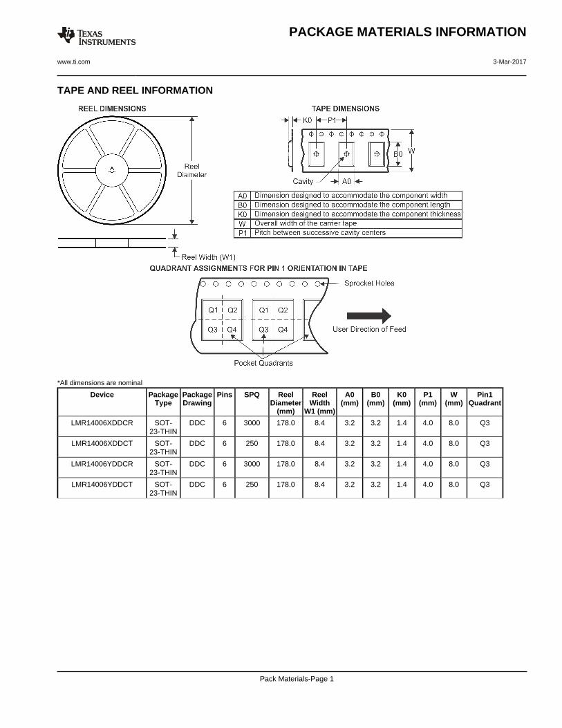
TAPE AND REEL INFORMATION
*All dimensions are nominal
Device PackageType
PackageDrawing
Pins SPQ ReelDiameter
(mm)
ReelWidth
W1 (mm)
A0(mm)
B0(mm)
K0(mm)
P1(mm)
W(mm)
Pin1Quadrant
LMR14006XDDCR SOT-23-THIN
DDC 6 3000 178.0 8.4 3.2 3.2 1.4 4.0 8.0 Q3
LMR14006XDDCT SOT-23-THIN
DDC 6 250 178.0 8.4 3.2 3.2 1.4 4.0 8.0 Q3
LMR14006YDDCR SOT-23-THIN
DDC 6 3000 178.0 8.4 3.2 3.2 1.4 4.0 8.0 Q3
LMR14006YDDCT SOT-23-THIN
DDC 6 250 178.0 8.4 3.2 3.2 1.4 4.0 8.0 Q3
PACKAGE MATERIALS INFORMATION
www.ti.com 3-Mar-2017
Pack Materials-Page 1
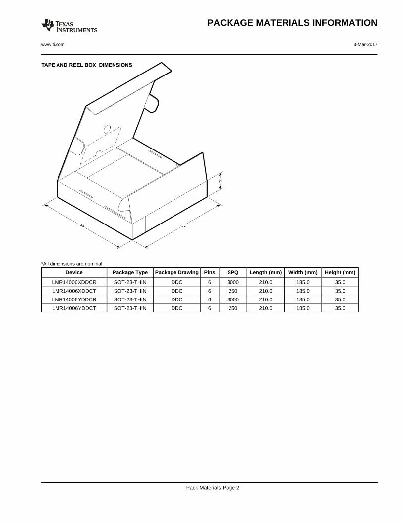
*All dimensions are nominal
Device Package Type Package Drawing Pins SPQ Length (mm) Width (mm) Height (mm)
LMR14006XDDCR SOT-23-THIN DDC 6 3000 210.0 185.0 35.0
LMR14006XDDCT SOT-23-THIN DDC 6 250 210.0 185.0 35.0
LMR14006YDDCR SOT-23-THIN DDC 6 3000 210.0 185.0 35.0
LMR14006YDDCT SOT-23-THIN DDC 6 250 210.0 185.0 35.0
PACKAGE MATERIALS INFORMATION
www.ti.com 3-Mar-2017
Pack Materials-Page 2


IMPORTANT NOTICE
Texas Instruments Incorporated (TI) reserves the right to make corrections, enhancements, improvements and other changes to itssemiconductor products and services per JESD46, latest issue, and to discontinue any product or service per JESD48, latest issue. Buyersshould obtain the latest relevant information before placing orders and should verify that such information is current and complete.TI’s published terms of sale for semiconductor products (http://www.ti.com/sc/docs/stdterms.htm) apply to the sale of packaged integratedcircuit products that TI has qualified and released to market. Additional terms may apply to the use or sale of other types of TI products andservices.Reproduction of significant portions of TI information in TI data sheets is permissible only if reproduction is without alteration and isaccompanied by all associated warranties, conditions, limitations, and notices. TI is not responsible or liable for such reproduceddocumentation. Information of third parties may be subject to additional restrictions. Resale of TI products or services with statementsdifferent from or beyond the parameters stated by TI for that product or service voids all express and any implied warranties for theassociated TI product or service and is an unfair and deceptive business practice. TI is not responsible or liable for any such statements.Buyers and others who are developing systems that incorporate TI products (collectively, “Designers”) understand and agree that Designersremain responsible for using their independent analysis, evaluation and judgment in designing their applications and that Designers havefull and exclusive responsibility to assure the safety of Designers' applications and compliance of their applications (and of all TI productsused in or for Designers’ applications) with all applicable regulations, laws and other applicable requirements. Designer represents that, withrespect to their applications, Designer has all the necessary expertise to create and implement safeguards that (1) anticipate dangerousconsequences of failures, (2) monitor failures and their consequences, and (3) lessen the likelihood of failures that might cause harm andtake appropriate actions. Designer agrees that prior to using or distributing any applications that include TI products, Designer willthoroughly test such applications and the functionality of such TI products as used in such applications.TI’s provision of technical, application or other design advice, quality characterization, reliability data or other services or information,including, but not limited to, reference designs and materials relating to evaluation modules, (collectively, “TI Resources”) are intended toassist designers who are developing applications that incorporate TI products; by downloading, accessing or using TI Resources in anyway, Designer (individually or, if Designer is acting on behalf of a company, Designer’s company) agrees to use any particular TI Resourcesolely for this purpose and subject to the terms of this Notice.TI’s provision of TI Resources does not expand or otherwise alter TI’s applicable published warranties or warranty disclaimers for TIproducts, and no additional obligations or liabilities arise from TI providing such TI Resources. TI reserves the right to make corrections,enhancements, improvements and other changes to its TI Resources. TI has not conducted any testing other than that specificallydescribed in the published documentation for a particular TI Resource.Designer is authorized to use, copy and modify any individual TI Resource only in connection with the development of applications thatinclude the TI product(s) identified in such TI Resource. NO OTHER LICENSE, EXPRESS OR IMPLIED, BY ESTOPPEL OR OTHERWISETO ANY OTHER TI INTELLECTUAL PROPERTY RIGHT, AND NO LICENSE TO ANY TECHNOLOGY OR INTELLECTUAL PROPERTYRIGHT OF TI OR ANY THIRD PARTY IS GRANTED HEREIN, including but not limited to any patent right, copyright, mask work right, orother intellectual property right relating to any combination, machine, or process in which TI products or services are used. Informationregarding or referencing third-party products or services does not constitute a license to use such products or services, or a warranty orendorsement thereof. Use of TI Resources may require a license from a third party under the patents or other intellectual property of thethird party, or a license from TI under the patents or other intellectual property of TI.TI RESOURCES ARE PROVIDED “AS IS” AND WITH ALL FAULTS. TI DISCLAIMS ALL OTHER WARRANTIES ORREPRESENTATIONS, EXPRESS OR IMPLIED, REGARDING RESOURCES OR USE THEREOF, INCLUDING BUT NOT LIMITED TOACCURACY OR COMPLETENESS, TITLE, ANY EPIDEMIC FAILURE WARRANTY AND ANY IMPLIED WARRANTIES OFMERCHANTABILITY, FITNESS FOR A PARTICULAR PURPOSE, AND NON-INFRINGEMENT OF ANY THIRD PARTY INTELLECTUALPROPERTY RIGHTS. TI SHALL NOT BE LIABLE FOR AND SHALL NOT DEFEND OR INDEMNIFY DESIGNER AGAINST ANY CLAIM,INCLUDING BUT NOT LIMITED TO ANY INFRINGEMENT CLAIM THAT RELATES TO OR IS BASED ON ANY COMBINATION OFPRODUCTS EVEN IF DESCRIBED IN TI RESOURCES OR OTHERWISE. IN NO EVENT SHALL TI BE LIABLE FOR ANY ACTUAL,DIRECT, SPECIAL, COLLATERAL, INDIRECT, PUNITIVE, INCIDENTAL, CONSEQUENTIAL OR EXEMPLARY DAMAGES INCONNECTION WITH OR ARISING OUT OF TI RESOURCES OR USE THEREOF, AND REGARDLESS OF WHETHER TI HAS BEENADVISED OF THE POSSIBILITY OF SUCH DAMAGES.Unless TI has explicitly designated an individual product as meeting the requirements of a particular industry standard (e.g., ISO/TS 16949and ISO 26262), TI is not responsible for any failure to meet such industry standard requirements.Where TI specifically promotes products as facilitating functional safety or as compliant with industry functional safety standards, suchproducts are intended to help enable customers to design and create their own applications that meet applicable functional safety standardsand requirements. Using products in an application does not by itself establish any safety features in the application. Designers mustensure compliance with safety-related requirements and standards applicable to their applications. Designer may not use any TI products inlife-critical medical equipment unless authorized officers of the parties have executed a special contract specifically governing such use.Life-critical medical equipment is medical equipment where failure of such equipment would cause serious bodily injury or death (e.g., lifesupport, pacemakers, defibrillators, heart pumps, neurostimulators, and implantables). Such equipment includes, without limitation, allmedical devices identified by the U.S. Food and Drug Administration as Class III devices and equivalent classifications outside the U.S.TI may expressly designate certain products as completing a particular qualification (e.g., Q100, Military Grade, or Enhanced Product).Designers agree that it has the necessary expertise to select the product with the appropriate qualification designation for their applicationsand that proper product selection is at Designers’ own risk. Designers are solely responsible for compliance with all legal and regulatoryrequirements in connection with such selection.Designer will fully indemnify TI and its representatives against any damages, costs, losses, and/or liabilities arising out of Designer’s non-compliance with the terms and provisions of this Notice.
Mailing Address: Texas Instruments, Post Office Box 655303, Dallas, Texas 75265Copyright © 2017, Texas Instruments Incorporated