Embed Size (px)
Citation preview

04/19/2304/19/23 Lecture 5Lecture 5 11
بسم الله بسم الله الرحمن الرحیمالرحمن الرحیمIn the name In the name
of godof god
04/19/2304/19/23 Lecture 5Lecture 5 22
ElectronicmicrElectronicmicro.mihanblog.co.mihanblog.c
omomدر این وبالگ سعی گردیده در این وبالگ سعی گردیده مطالبی ارایه گردد که برای مطالبی ارایه گردد که برای دانشجویان دوره کاردانی دانشجویان دوره کاردانی مثمر ثمر بوده و یاور آنان مثمر ثمر بوده و یاور آنان
..باشدباشد..مطالب جدید نیز در راه استمطالب جدید نیز در راه است
این فایل به صورت زبان این فایل به صورت زبان اصلی به دانشجو ارایه میگردد اصلی به دانشجو ارایه میگردد
امید است که بهروری الزم امید است که بهروری الزم ببردببرد..را را

04/19/2304/19/23 Lecture 5Lecture 5 33
Contents of this Lecture: Outlines of signal conditioning circuits
design: amplification and filtering
Learn from Examples

WhyWhy Need Signal Amplification?Need Signal Amplification?
04/19/2304/19/23 Lecture 5Lecture 5 44

Outlines of Signal AmplifiersOutlines of Signal Amplifiers
Designed to amplify input signals to a right level to be noticeable for further uses.
Typical input signals are: thermocouple, RTD, pressure, strain, flow, pH, etc.
Typical outputs include: high level dc voltages (0 to 5 or 0 to 10 volts), process current (0 to 20 mA or 4 to 20 mA)
There are commercial signal conditioners with computer interface ready.
04/19/2304/19/23 Lecture 5Lecture 5 55
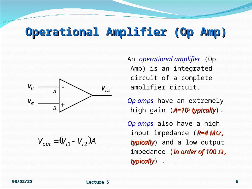
Operational Amplifier (Op Amp)Operational Amplifier (Op Amp)
An operational amplifier (Op Amp) is an integrated circuit of a complete amplifier circuit.
Op amps have an extremely high gain (A=10A=1055 typically typically).
Op amps also have a high input impedance (R=4 MR=4 M , ,
typicallytypically) and a low output impedance (in order of 100 in order of 100
, typically, typically) .
04/19/2304/19/23 Lecture 5Lecture 5 66
-
+
Vi1 VoutA
B
Vi2
AVVV iiout 21

Characters of Operational Characters of Operational Amplifiers Amplifiers
high open loop gain
high input impedance
low output impedance
low input offset voltage
low temperature coefficient of input offset voltage
low input bias current
wide bandwidth
large common mode rejection ratio (CMRR)
04/19/2304/19/23 Lecture 5Lecture 5 77
11 22 33 44
88 77 66 55
Offset nullOffset null
Offset nullOffset nullNot usedNot used

Voltage Output from an AmplifierVoltage Output from an Amplifier
The linear range of an amplifier is finite, and limited by the supply voltage and the characteristics of the amplifier.
If an amplifier is driven beyond the linear range (overdrivenoverdriven), serious errors can result if the gain is treated as a constant.
04/19/2304/19/23 Lecture 5Lecture 5 88
AA
LinearLinearregionregion
Non-linearNon-linearregionregion
VVoutout
VVinin
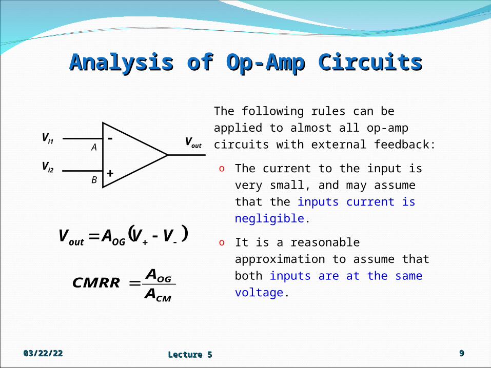
Analysis of Op-Amp CircuitsAnalysis of Op-Amp Circuits
The following rules can be applied to almost all op-amp circuits with external feedback:
o The current to the input is very small, and may assume that the inputs current is negligible.
o It is a reasonable approximation to assume that both inputs are at the same voltage.
04/19/2304/19/23 Lecture 5Lecture 5 99
-
+
Vi1 VoutA
B
Vi2
VVAV OGout
CM
OG
A
ACMRR

Ideal Amplifiers with or without Ideal Amplifiers with or without feedbackfeedback
04/19/2304/19/23 Lecture 5Lecture 5 1010
1
2
VV
G
1
2
VV
G VVSS
VV11 VV22
1
2
VV
G VVSS
VV11 VV22
R1
R2
VVFF
An ideal op-amp has very high open gain at 0 Hz.
Actual amplifier commonly hasexternal feedback.
FS VVV 1
21
1
2 RRR
VV
H F
HGHG
VV
AS
11
2
2112 HVVGGVV

Inverting AmplifierInverting Amplifier
Point B is grounded, so does point A (very small).
Voltage across R1 is Vin, and
across RF is Vout.
The output node voltage determined by Kirchhoff's Current Law (KCL).
Circuit voltage gain determined by the ratio of
R1 and RF.
04/19/2304/19/23 Lecture 5Lecture 5 1111
1R
R
V
VG F
in
out
-
+
Vin
Vout
R1
RF
A
B
F
F
RRRR
R
1
13

Analysis of Inverting AmplifierAnalysis of Inverting Amplifier
Ideal transfer characteristics:Ideal transfer characteristics:
04/19/2304/19/23 Lecture 5Lecture 5 1212
-
+
Vin
Vout
R1
RF
A
BR
ii++
VV++
iiFF
ii11
ii--
VV--
0 ii
VV
OG
OGout
A
VVAV
FF iiii 1
F
outF
IN
R
VViand
R
VVi
11
000 VVi
F
outIN
R
V
R
V
1oror
1R
R
V
V F
in
out

Noninverting AmplifierNoninverting Amplifier
Op-amp circuit is a voltage divider.
04/19/2304/19/23 Lecture 5Lecture 5 1313
-
+Vin
Vout
R1
RF
A
BF
outA RR
RVV
1
1
1
1R
R
V
VG F
in
out
Circuit voltage gain determined by the ratio of R1 and RF.
Point VA equals to Vin .

Differential AmplifierDifferential Amplifier
Point B is grounded, so does point A (very small).
Voltage across R1 is V1, and
across R2 is V2.
Normally: R1 = R2, and RF
= R3.
Commonly used as a single op-amp instrumentation amplifier.
04/19/2304/19/23 Lecture 5Lecture 5 1414
)( 121
VVR
RV Fout
RF
-
+
V1
Vout
R1
A
BR3
V2
R2

Design an Instrumentation Design an Instrumentation AmplifierAmplifier
Design a single op-amp instrumentation amplifier.
R1 = R2, RF = R3
Determine the instrumentation gain.
04/19/2304/19/23 Lecture 5Lecture 5 1515
-
+
V1
Vout
R1
RF
A
B
R3
V2
R2A
F
OUTAA iR
VV
R
VV
1
1
32
2
R
Vi
R
VV BB
B
0 BA ii
2
2
31
1
R
VV
R
V
R
VV
R
VV BB
F
OUTAA
1
12
R
VVVV
R
VVV BA
F
BAOUT
)( 121
VVR
RV Fout
BA VV

Instrumentation amplifierInstrumentation amplifier
04/19/2304/19/23 Lecture 5Lecture 5 1616
15
621R
R
R
RA Fd
Difference Gain:Difference Gain:
R6
R5R6
-
+
+
-
V2
V1
Vcm
-
+ Vout
R1
RF
R3
R2
VB
VA
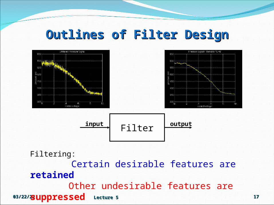
Outlines of Filter DesignOutlines of Filter Design
04/19/2304/19/23 Lecture 5Lecture 5 1717
Filterinput output
Filtering: Certain desirable features are retained Other undesirable features are suppressed

Classification of FiltersClassification of Filters
04/19/2304/19/23 Lecture 5Lecture 5 1818
Signal Filter
Analog Filter Digital Filter
Element Type Frequency Band
Active Passive Low-Pass
High-Pass
Band-Pass
Band-Reject
All-Pass

Terminology in Filter DesignTerminology in Filter Design
Signal-To-Noise Ratio (S/N)
04/19/2304/19/23 Lecture 5Lecture 5 1919
dBW
WNS
N
S
log10
Bandwidththe range of frequencies of |G(j)|>0.707
Cutoff Frequency
the end of pass-band frequency Break-point of a filter
the point with a gain of -3dB

Passive Low-Pass FilterPassive Low-Pass Filter
The pass-band is from 0 to some frequency wp.
Its stop-band extends form some frequency ws, to infinity.
In practical circuit design, engineers often choose amplitude gain of 0.95 for passive RC filters:
04/19/2304/19/23 Lecture 5Lecture 5 2020
p s
)( jH
Vout
Vin
C
R
VVoutoutVVinin RL

Passive High-Pass FilterPassive High-Pass Filter
Its stop-band is form 0 to some frequency s
The pass-band is from some frequency p to infinity.
In practical circuit design, engineers choose amplitude gain of 0.95 for passive CR filters:
04/19/2304/19/23 Lecture 5Lecture 5 2121
s p
)( jH
Vout
Vin
R
C
VVoutoutVVinin

Design of Passive FiltersDesign of Passive Filters
04/19/2304/19/23 Lecture 5Lecture 5 2222
1
1
jRCjH
1
1
RCs
sH
Transfer Function
21
1
RCV
V
in
out
The amplitude response:
2
1
2
13
RCf dB
The 3dB break-point is at:
LF
L
ZZ
ZG
The amplitude gain:
C
R
VVoutoutVVinin RL

Guideline of Pass Filter DesignGuideline of Pass Filter Design
04/19/2304/19/23 Lecture 5Lecture 5 2323
R
1
1
s
sH
Transfer Function
C VVoutoutVVinin RL
RC
Time Constant
Select resistor based on amplitude gain:
95.0
LF
L
ZZ
ZG
LLF RZRZ 053.095.0
05.0
Select capacitor based on cut-off freq:
dBRfRC
32
1
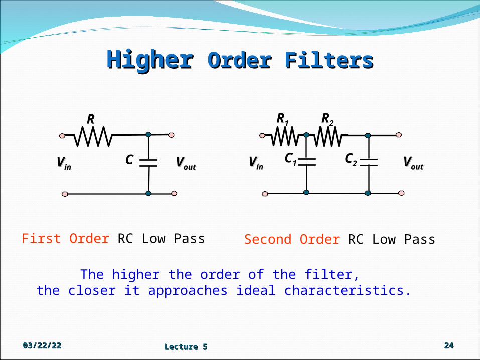
Higher Higher Order FiltersOrder Filters
04/19/2304/19/23 Lecture 5Lecture 5 2424
C
R
VVoutoutVVinin
First Order RC Low Pass Second Order RC Low Pass
C2 VVoutoutVVininC1
R1 R2
The higher the order of the filter, the closer it approaches ideal characteristics.

Active FiltersActive Filters
Active filters employ Op-Amps to attenuate select frequencies and amplify signal during filtering process.
Q factor of a filter is defined as the ratio of the center frequency fc to the bandwidth fH - fL :
04/19/2304/19/23 Lecture 5Lecture 5 2525
LH
Cff
fQ

Design of Low Pass Active FiltersDesign of Low Pass Active Filters
Example:Design a low pass filter with cut-off frequency of 5kHz, and DC gain of 10:
Two equations, three unknowns
04/19/2304/19/23 Lecture 5Lecture 5 2626
-
+
Vin
Vout
R1
RF
A
B
C2
Transfer Function: Transfer Function:
0
0..
s
KFT LP
221
CRfF
H
The -3 dB cut-off frequency:
1RRK F
LP
The DC gain:

Design of High Pass Active FiltersDesign of High Pass Active Filters
The -3 dB cut-off frequency:
The DC gain:
Two equations, three unknowns
Select one component based on other conditions, and determine the values of the other two components.
04/19/2304/19/23 Lecture 5Lecture 5 2727
Vout
-
+
Vin
R1
RF
A
B
C1
1121
CRfH
1RRK F
HP
Transfer Function: Transfer Function:
0
..
s
sKFT HP

Filter ClassFilter Class
o A filter of a given order can be made to approximate to ideal characteristics in a number of ways, depending on the values of the filter components (or say: depending on the filter class.
o Two useful classes are Butterworth (maximally flat) and Chebyshev (equal-ripple) filters (n is the filter order)
04/19/2304/19/23 Lecture 5Lecture 5 2828
n
C
in
out
ffV
V2
1
1
Butterworth Filter
Chebyshev Filter
Cn
in
out
ffCEV
V
221
1

Higher Order Active FiltersHigher Order Active Filters
04/19/2304/19/23 Lecture 5Lecture 5 2929
Vout
-
+Vin
R2
Rb
C1
R1
Ra
C2
Gain=K
Filter Class R1 R2 C1 C2 K
Buterworth3.01 dB at H
1.00 1.001.001.00 1.59
Chebyshev1 dB ripple
1.00 1.000.94 0.97 2.00
The above list gives the gain and component valves for one of themany choices for H=1. You may find more combinations from filter design handbook(s).
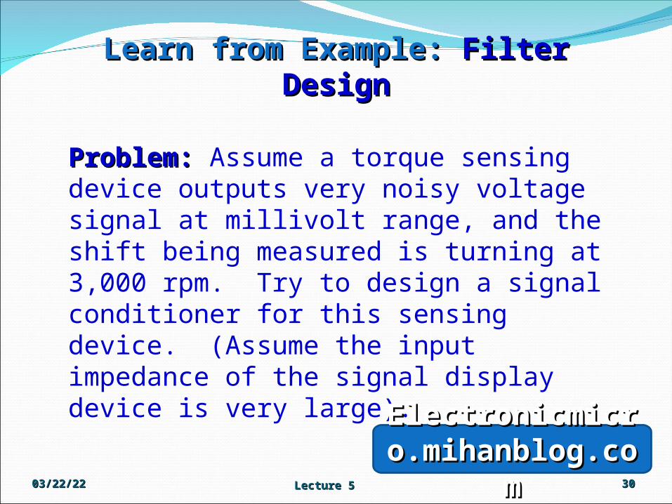
Learn from Example: Learn from Example: Filter Filter DesignDesign
04/19/2304/19/23 Lecture 5Lecture 5 3030
Problem:Problem: Assume a torque sensing device outputs very noisy voltage signal at millivolt range, and the shift being measured is turning at 3,000 rpm. Try to design a signal conditioner for this sensing device. (Assume the input impedance of the signal display device is very large).
ElectronicmicrElectronicmicro.mihanblog.coo.mihanblog.co
mm