Embed Size (px)
Citation preview
AR0130: 1/3-Inch CMOS Digital Image SensorFeatures
‡
1/3-Inch CMOS Digital Image SensorAR0130 Datasheet, Rev. L
For the latest datasheet, please visit www.onsemi.com
Features• Superior low-light performance both in VGA mode
and HD mode• Excellent Near IR performance• HD video (720p60)• On-chip AE and statistics engine• Auto black level calibration• Context switching• Progressive Scan• Supports 2:1 scaling• Internal master clock generated by on-chip phase
locked loop (PLL) oscillator. • Parallel output
Applications• Gaming systems• Video surveillance• 720p60 video applications
General DescriptionON Semiconductor's AR0130 is a 1/3-inch CMOS digi-tal image sensor with an active-pixel array of 1280H x 960V. It captures images with a rolling-shutter readout. It includes sophisticated camera functions such as auto exposure control, windowing, and both video and single frame modes. It is programmable through a sim-ple two-wire serial interface. The AR0130 produces extraordinarily clear, sharp digital pictures, and its ability to capture both continuous video and single frames makes it the perfect choice for a wide range of applications, including gaming systems, surveillance, and HD video.
AR0130 DS Rev. L Pub. 6/15 EN 1
Table 1: Key Parameters
Parameter Typical Value
Optical format 1/3-inch (6 mm)
Active pixels 1280 x 960 = 1.2 Mp
Pixel size 3.75 m
Color filter array Monochrome, RGB Bayer
Shutter type Electronic rolling shutter
Input clock range 6 – 50 MHz
Output clock maximum 74.25 MHz
Output Parallel 12-bit
Max. Frame rates
1.2 Mp (full FOV) 45 fps
720pHD (reduced FOV) 60 fps
VGA (full FOV) 45 fps
VGA (reduced FOV) 60 fps
800 x 800 (reduced FOV)
60 fps
Responsivity at 550 nm (Mono) 6.5 V/lux-sec
Responsivity at 550 nm (RGB green)
5.6 V/lux-sec
SNRMAX 44 dB
Dynamic range 82 dB
Supply voltage
I/O 1.8 or 2.8 V
Digital 1.8 V
Analog 2.8 V
Power consumption270 mW (1280x720 60 fps)
Operating temperature–30°C to + 70°C (ambient)–30°C to + 80°C ( junction)
Package option Bare die, iLCC, PLCC
©Semiconductor Components Industries, LLC 2015,
AR0130: 1/3-Inch CMOS Digital Image SensorOrdering Information
Ordering Information
See the ON Semiconductor Device Nomenclature document (TND310/D) for a full description of the naming convention used for image sensors. For reference documenta-tion, including information on evaluation kits, please visit our web site at www.onsemi.com.
Table 2: Available Part Numbers
Part Number Base Description Variant Description
AR0130CSSC00SPBA0-DP RGB Bayer 48-Pin PLCC Dry Pack with Protective Film
AR0130CSSC00SPBA0-DR RGB Bayer 48-Pin PLCC Dry Pack without Protective Film
AR0130CSSC00SPCA0-DPBR RGB Bayer 48-Pin iLCC Dry Pack with Protective Film, Double Side BBAR Glass
AR0130CSSC00SPCA0-DRBR RGB Bayer 48-Pin iLCC Dry Pack without Protective Film, Double Side BBAR Glass
AR0130CSSC00SPCAD3-GEVK RGB Bayer demo kit iLCC
AR0130CSSC00SPCAD3-S115-GEVK RGB Bayer demo kit iLCC
AR0130CSSC00SPCAD3-S213A-GEVK RGB Bayer demo kit iLCC
AR0130CSSC00SPCAD-GEVK RGB Bayer demo kit iLCC
AR0130CSSC00SPCAD-S115-GEVK RGB Bayer demo kit iLCC
AR0130CSSC00SPCAD-S213A-GEVK RGB Bayer demo kit iLCC
AR0130CSSC00SPCAH-GEVB RGB Bayer headboard iLCC
AR0130CSSC00SPCAH-S115-GEVB RGB Bayer headboard iLCC
AR0130CSSC00SPCAH-S213A-GEVB RGB Bayer headboard iLCC
AR0130CSSC00SPCAW-GEVB RGB Bayer headboard iLCC
AR0130CSSM00SPCA0-DRBR Monochrome 48-Pin iLCC Dry Pack without Protective Film, Double Side BBAR Glass
AR0130CSSM00SPCAD-S213A-GEVK Monochrome demo kit iLCC
AR0130CSSM00SPCAH-S213A-GEVB Monochrome headboard iLCC
AR0130 DS Rev. L Pub. 6/15 EN 2 ©Semiconductor Components Industries, LLC, 2015.
AR0130 DS Rev. L Pub. 6/15 EN 3 ©Semiconductor Components Industries, LLC, 2015.
AR0130: 1/3-Inch CMOS Digital Image SensorTable of Contents
Table of Contents
Features . . . . . . . . . . . . . . . . . . . . . . . . . . . . . . . . . . . . . . . . . . . . . . . . . . . . . . . . . . . . . . . . . . . . . . . . . . . . . . . . . . . . . . . . . . . . . .1Applications . . . . . . . . . . . . . . . . . . . . . . . . . . . . . . . . . . . . . . . . . . . . . . . . . . . . . . . . . . . . . . . . . . . . . . . . . . . . . . . . . . . . . . . . . .1General Description . . . . . . . . . . . . . . . . . . . . . . . . . . . . . . . . . . . . . . . . . . . . . . . . . . . . . . . . . . . . . . . . . . . . . . . . . . . . . . . . . . .1Ordering Information. . . . . . . . . . . . . . . . . . . . . . . . . . . . . . . . . . . . . . . . . . . . . . . . . . . . . . . . . . . . . . . . . . . . . . . . . . . . . . . . . .2General Description . . . . . . . . . . . . . . . . . . . . . . . . . . . . . . . . . . . . . . . . . . . . . . . . . . . . . . . . . . . . . . . . . . . . . . . . . . . . . . . . . . .6Functional Overview. . . . . . . . . . . . . . . . . . . . . . . . . . . . . . . . . . . . . . . . . . . . . . . . . . . . . . . . . . . . . . . . . . . . . . . . . . . . . . . . . . .6Pixel Data Format . . . . . . . . . . . . . . . . . . . . . . . . . . . . . . . . . . . . . . . . . . . . . . . . . . . . . . . . . . . . . . . . . . . . . . . . . . . . . . . . . . . .11Output Data Format . . . . . . . . . . . . . . . . . . . . . . . . . . . . . . . . . . . . . . . . . . . . . . . . . . . . . . . . . . . . . . . . . . . . . . . . . . . . . . . . . .13Real-Time Context Switching . . . . . . . . . . . . . . . . . . . . . . . . . . . . . . . . . . . . . . . . . . . . . . . . . . . . . . . . . . . . . . . . . . . . . . . . . .17Features . . . . . . . . . . . . . . . . . . . . . . . . . . . . . . . . . . . . . . . . . . . . . . . . . . . . . . . . . . . . . . . . . . . . . . . . . . . . . . . . . . . . . . . . . . . . .17Two-Wire Serial Register Interface . . . . . . . . . . . . . . . . . . . . . . . . . . . . . . . . . . . . . . . . . . . . . . . . . . . . . . . . . . . . . . . . . . . . .32Spectral Characteristics . . . . . . . . . . . . . . . . . . . . . . . . . . . . . . . . . . . . . . . . . . . . . . . . . . . . . . . . . . . . . . . . . . . . . . . . . . . . . . .36Package Dimensions . . . . . . . . . . . . . . . . . . . . . . . . . . . . . . . . . . . . . . . . . . . . . . . . . . . . . . . . . . . . . . . . . . . . . . . . . . . . . . . . .38Electrical Specifications. . . . . . . . . . . . . . . . . . . . . . . . . . . . . . . . . . . . . . . . . . . . . . . . . . . . . . . . . . . . . . . . . . . . . . . . . . . . . . .40Power-On Reset and Standby Timing. . . . . . . . . . . . . . . . . . . . . . . . . . . . . . . . . . . . . . . . . . . . . . . . . . . . . . . . . . . . . . . . . . .48Revision History. . . . . . . . . . . . . . . . . . . . . . . . . . . . . . . . . . . . . . . . . . . . . . . . . . . . . . . . . . . . . . . . . . . . . . . . . . . . . . . . . . . . . .51
AR0130 DS Rev. L Pub. 6/15 EN 4 ©Semiconductor Components Industries, LLC, 2015.
AR0130: 1/3-Inch CMOS Digital Image SensorList of Figures
List of Figures
Figure 1: Block Diagram . . . . . . . . . . . . . . . . . . . . . . . . . . . . . . . . . . . . . . . . . . . . . . . . . . . . . . . . . . . . . . . . . . . . . . . . . . . .6Figure 2: Typical Configuration: Parallel Pixel Data Interface . . . . . . . . . . . . . . . . . . . . . . . . . . . . . . . . . . . . . . . . . . .7Figure 3: 48-Pin iLCC Pinout Diagram . . . . . . . . . . . . . . . . . . . . . . . . . . . . . . . . . . . . . . . . . . . . . . . . . . . . . . . . . . . . . . .9Figure 4: 48-Pin PLCC Pinout Diagram. . . . . . . . . . . . . . . . . . . . . . . . . . . . . . . . . . . . . . . . . . . . . . . . . . . . . . . . . . . . . .10Figure 5: Pixel Array Description . . . . . . . . . . . . . . . . . . . . . . . . . . . . . . . . . . . . . . . . . . . . . . . . . . . . . . . . . . . . . . . . . . .11Figure 6: Pixel Color Pattern Detail (Top Right Corner) . . . . . . . . . . . . . . . . . . . . . . . . . . . . . . . . . . . . . . . . . . . . . . .12Figure 7: Imaging a Scene . . . . . . . . . . . . . . . . . . . . . . . . . . . . . . . . . . . . . . . . . . . . . . . . . . . . . . . . . . . . . . . . . . . . . . . . .12Figure 8: Spatial Illustration of Image Readout. . . . . . . . . . . . . . . . . . . . . . . . . . . . . . . . . . . . . . . . . . . . . . . . . . . . . . .13Figure 9: Default Pixel Output Timing . . . . . . . . . . . . . . . . . . . . . . . . . . . . . . . . . . . . . . . . . . . . . . . . . . . . . . . . . . . . . .14Figure 10: LV Format Options . . . . . . . . . . . . . . . . . . . . . . . . . . . . . . . . . . . . . . . . . . . . . . . . . . . . . . . . . . . . . . . . . . . . . . .14Figure 11: Line Timing and FRAME_VALID/LINE_VALID Signals . . . . . . . . . . . . . . . . . . . . . . . . . . . . . . . . . . . . . . .15Figure 12: PLL-Generated Master Clock PLL Setup . . . . . . . . . . . . . . . . . . . . . . . . . . . . . . . . . . . . . . . . . . . . . . . . . . . .18Figure 13: Enter Standby Timing . . . . . . . . . . . . . . . . . . . . . . . . . . . . . . . . . . . . . . . . . . . . . . . . . . . . . . . . . . . . . . . . . . . .20Figure 14: Exit Standby Timing. . . . . . . . . . . . . . . . . . . . . . . . . . . . . . . . . . . . . . . . . . . . . . . . . . . . . . . . . . . . . . . . . . . . . .20Figure 15: Six Pixels in Normal and Column Mirror Readout Modes. . . . . . . . . . . . . . . . . . . . . . . . . . . . . . . . . . . . .22Figure 16: Six Rows in Normal and Row Mirror Readout Modes . . . . . . . . . . . . . . . . . . . . . . . . . . . . . . . . . . . . . . . .23Figure 17: Frame Format with Embedded Data Lines Enabled . . . . . . . . . . . . . . . . . . . . . . . . . . . . . . . . . . . . . . . . .26Figure 18: Format of Embedded Data Output within a Frame . . . . . . . . . . . . . . . . . . . . . . . . . . . . . . . . . . . . . . . . . .27Figure 19: Format of Embedded Statistics Output within a Frame. . . . . . . . . . . . . . . . . . . . . . . . . . . . . . . . . . . . . . .28Figure 20: Single READ from Random Location . . . . . . . . . . . . . . . . . . . . . . . . . . . . . . . . . . . . . . . . . . . . . . . . . . . . . . .34Figure 21: Single READ from Current Location. . . . . . . . . . . . . . . . . . . . . . . . . . . . . . . . . . . . . . . . . . . . . . . . . . . . . . . .34Figure 22: Sequential READ, Start from Random Location . . . . . . . . . . . . . . . . . . . . . . . . . . . . . . . . . . . . . . . . . . . . .34Figure 23: Sequential READ, Start from Current Location . . . . . . . . . . . . . . . . . . . . . . . . . . . . . . . . . . . . . . . . . . . . . .35Figure 24: Single WRITE to Random Location. . . . . . . . . . . . . . . . . . . . . . . . . . . . . . . . . . . . . . . . . . . . . . . . . . . . . . . . .35Figure 25: Sequential WRITE, Start at Random Location . . . . . . . . . . . . . . . . . . . . . . . . . . . . . . . . . . . . . . . . . . . . . . .35Figure 26: Quantum Efficiency – Monochrome Sensor. . . . . . . . . . . . . . . . . . . . . . . . . . . . . . . . . . . . . . . . . . . . . . . . .36Figure 27: Quantum Efficiency – Color Sensor . . . . . . . . . . . . . . . . . . . . . . . . . . . . . . . . . . . . . . . . . . . . . . . . . . . . . . . .37Figure 28: 48 iLCC Package Outline Drawing . . . . . . . . . . . . . . . . . . . . . . . . . . . . . . . . . . . . . . . . . . . . . . . . . . . . . . . . .38Figure 29: 48 PLCC Package Outline Drawing . . . . . . . . . . . . . . . . . . . . . . . . . . . . . . . . . . . . . . . . . . . . . . . . . . . . . . . . .39Figure 30: Two-Wire Serial Bus Timing Parameters. . . . . . . . . . . . . . . . . . . . . . . . . . . . . . . . . . . . . . . . . . . . . . . . . . . .40Figure 31: I/O Timing Diagram. . . . . . . . . . . . . . . . . . . . . . . . . . . . . . . . . . . . . . . . . . . . . . . . . . . . . . . . . . . . . . . . . . . . . .42Figure 32: Power Supply Rejection Ratio . . . . . . . . . . . . . . . . . . . . . . . . . . . . . . . . . . . . . . . . . . . . . . . . . . . . . . . . . . . . .47Figure 33: Power Up . . . . . . . . . . . . . . . . . . . . . . . . . . . . . . . . . . . . . . . . . . . . . . . . . . . . . . . . . . . . . . . . . . . . . . . . . . . . . . .48Figure 34: Power Down. . . . . . . . . . . . . . . . . . . . . . . . . . . . . . . . . . . . . . . . . . . . . . . . . . . . . . . . . . . . . . . . . . . . . . . . . . . . .50
AR0130 DS Rev. L Pub. 6/15 EN 5 ©Semiconductor Components Industries, LLC, 2015.
AR0130: 1/3-Inch CMOS Digital Image SensorList of Tables
List of Tables
Table 1: Key Parameters . . . . . . . . . . . . . . . . . . . . . . . . . . . . . . . . . . . . . . . . . . . . . . . . . . . . . . . . . . . . . . . . . . . . . . . . . . .1Table 2: Available Part Numbers. . . . . . . . . . . . . . . . . . . . . . . . . . . . . . . . . . . . . . . . . . . . . . . . . . . . . . . . . . . . . . . . . . . .2Table 3: Pad Descriptions. . . . . . . . . . . . . . . . . . . . . . . . . . . . . . . . . . . . . . . . . . . . . . . . . . . . . . . . . . . . . . . . . . . . . . . . . .8Table 4: Frame Time (Example Based on 1280 x 960, 45 Frames Per Second) . . . . . . . . . . . . . . . . . . . . . . . . . . .15Table 5: Frame Time: Long Integration Time . . . . . . . . . . . . . . . . . . . . . . . . . . . . . . . . . . . . . . . . . . . . . . . . . . . . . . .16Table 6: Real-Time Context-Switchable Registers . . . . . . . . . . . . . . . . . . . . . . . . . . . . . . . . . . . . . . . . . . . . . . . . . . .17Table 7: Test Pattern Modes. . . . . . . . . . . . . . . . . . . . . . . . . . . . . . . . . . . . . . . . . . . . . . . . . . . . . . . . . . . . . . . . . . . . . . .31Table 8: Two-Wire Serial Bus Characteristics . . . . . . . . . . . . . . . . . . . . . . . . . . . . . . . . . . . . . . . . . . . . . . . . . . . . . . .41Table 9: I/O Timing Characteristics (2.8V VDD_IO)1 . . . . . . . . . . . . . . . . . . . . . . . . . . . . . . . . . . . . . . . . . . . . . . . . . . . . . . . . . . . . . .42
Table 10: I/O Timing Characteristics (1.8V VDD_IO)1 . . . . . . . . . . . . . . . . . . . . . . . . . . . . . . . . . . . . . . . . . . . . . . . . . . . . . . . . . . . . . .43
Table 11: I/O Rise Slew Rate (2.8V VDD_IO)1 . . . . . . . . . . . . . . . . . . . . . . . . . . . . . . . . . . . . . . . . . . . . . . . . . . . . . . . . . . . . . . . . . . . . . . . .44
Table 12: I/O Fall Slew Rate (2.8V VDD_IO)1. . . . . . . . . . . . . . . . . . . . . . . . . . . . . . . . . . . . . . . . . . . . . . . . . . . . . . . . . . . . . . . . . . . . . . . . .44
Table 13: I/O Rise Slew Rate (1.8V VDD_IO)1 . . . . . . . . . . . . . . . . . . . . . . . . . . . . . . . . . . . . . . . . . . . . . . . . . . . . . . . . . . . . . . . . . . . . . . . .44
Table 14: I/O Fall Slew Rate (1.8V VDD_IO)1. . . . . . . . . . . . . . . . . . . . . . . . . . . . . . . . . . . . . . . . . . . . . . . . . . . . . . . . . . . . . . . . . . . . . . . . .45
Table 15: DC Electrical Characteristics . . . . . . . . . . . . . . . . . . . . . . . . . . . . . . . . . . . . . . . . . . . . . . . . . . . . . . . . . . . . . .45Table 16: Absolute Maximum Ratings . . . . . . . . . . . . . . . . . . . . . . . . . . . . . . . . . . . . . . . . . . . . . . . . . . . . . . . . . . . . . . .46Table 17: Operating Current Consumption in Parallel Output . . . . . . . . . . . . . . . . . . . . . . . . . . . . . . . . . . . . . . . .46Table 18: Standby Current Consumption . . . . . . . . . . . . . . . . . . . . . . . . . . . . . . . . . . . . . . . . . . . . . . . . . . . . . . . . . . .47Table 19: Power-Up Sequence. . . . . . . . . . . . . . . . . . . . . . . . . . . . . . . . . . . . . . . . . . . . . . . . . . . . . . . . . . . . . . . . . . . . . .49Table 20: Power-Down Sequence . . . . . . . . . . . . . . . . . . . . . . . . . . . . . . . . . . . . . . . . . . . . . . . . . . . . . . . . . . . . . . . . . . .50
AR0130: 1/3-Inch CMOS Digital Image SensorGeneral Description
General DescriptionThe ON Semiconductor AR0130 can be operated in its default mode or programmed for frame size, exposure, gain, and other parameters. The default mode output is a 960p-resolution image at 45 frames per second (fps). It outputs 12-bit raw data over the parallel port. The device may be operated in video (master) mode or in single frame trigger mode.
FRAME_VALID and LINE_VALID signals are output on dedicated pins, along with a synchronized pixel clock in parallel mode.
The AR0130 includes additional features to allow application-specific tuning: windowing and offset, adjustable auto-exposure control, and auto black level correction. Optional register information and histogram statistic information can be embedded in first and last 2 lines of the image frame.
Functional OverviewThe AR0130 is a progressive-scan sensor that generates a stream of pixel data at a constant frame rate. It uses an on-chip, phase-locked loop (PLL) that can be optionally enabled to generate all internal clocks from a single master input clock running between 6 and 50 MHz The maximum output pixel rate is 74.25 Mp/s, corresponding to a clock rate of 74.25 MHz. Figure 1 shows a block diagram of the sensor.
Figure 1: Block Diagram
User interaction with the sensor is through the two-wire serial bus, which communi-cates with the array control, analog signal chain, and digital signal chain. The core of the sensor is a 1.2 Mp Active- Pixel Sensor array. The timing and control circuitry sequences through the rows of the array, resetting and then reading each row in turn. In the time interval between resetting a row and reading that row, the pixels in the row integrate incident light. The exposure is controlled by varying the time interval between reset and readout. Once a row has been read, the data from the columns is sequenced through an analog signal chain (providing offset correction and gain), and then through an analog-to-digital converter (ADC). The output from the ADC is a 12-bit value for each pixel in the array. The ADC output passes through a digital processing signal chain (which
Control Registers
Active Pixel Sensor (APS)Array
PLLMemoryOTPM
Timing and Control(Sequencer)
Analog Processing and A/D Conversion
Auto Exposureand Stats Engine
Pixel Data Path(Signal Processing)
ExternalClock
ParallelOutput
Two-WireSerial
Interface
Trigger
Power
AR0130 DS Rev. L Pub. 6/15 EN 6 ©Semiconductor Components Industries, LLC, 2015.
AR0130: 1/3-Inch CMOS Digital Image SensorFunctional Overview
provides further data path corrections and applies digital gain). The pixel data are output at a rate of up to 74.25 Mp/s, in parallel to frame and line synchronization signals.
Figure 2: Typical Configuration: Parallel Pixel Data Interface
Notes: 1. All power supplies must be adequately decoupled.2. ON Semiconductor recommends a resistor value of 1.5k, but a greater value may be used for
slower two-wire speed.3. This pull-up resistor is not required if the controller drives a valid logic level on SCLK at all times.4. ON Semiconductor recommends that VDD_SLVS pad (only available in bare die) is left unconnected.5. ON Semiconductor recommends that 0.1μF and 10μF decoupling capacitors for each power supply
are mounted as close as possible to the pad. Actual values and results may vary depending on lay-out and design considerations. Check the AR0130 demo headboard schematics for circuit recom-mendations.
6. ON Semiconductor recommends that analog power planes are placed in a manner such that cou-pling with the digital power planes is minimized.
7. I/O signals voltage must be configured to match VDD_IO voltage to minimize any leakage currents.
VDD
Master clock(6–50 MHz)
SDATASCLK
Reserved
FRAME_VALID
DOUT [11:0]EXTCLK
DGND
Digitalground
Analogground
Digitalcore
power1
Tocontroller
FromController
LINE_VALID
PIXCLK
RESET_BAR
VDD_IO
DigitalI/O
power1
1.5kΩ
2
1.5kΩ
2, 3 VAA VAA_PIX
Analogpower1
VDD_PLL
PLLpower1
Analogpower1
VAA_PIXVDD_IO VDD_PLLVDD VAA
TRIGGEROE_BARSTANDBY
AGND
SADDR
AR0130 DS Rev. L Pub. 6/15 EN 7 ©Semiconductor Components Industries, LLC, 2015.
AR0130: 1/3-Inch CMOS Digital Image SensorFunctional Overview
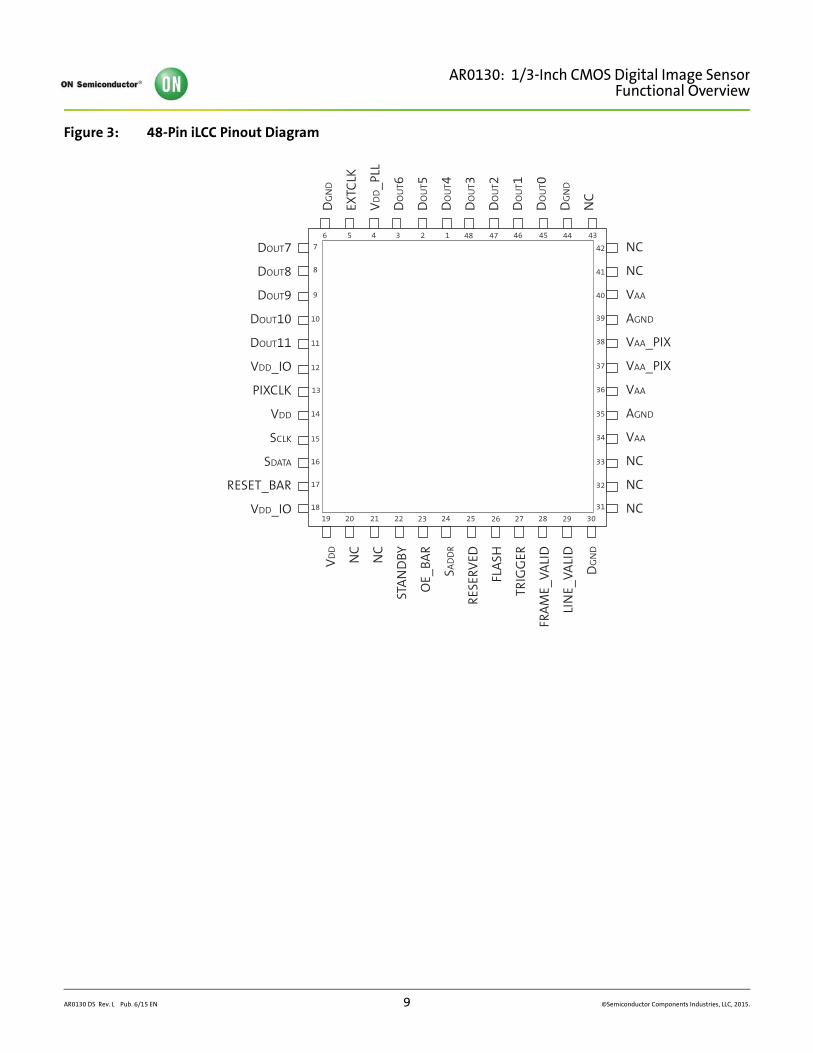
Table 3: Pad Descriptions
Name Type Description
STANDBY Input Standby-mode enable pin (active HIGH).
VDD_PLL Power PLL power.
VAA Power Analog power.
EXTCLK Input External input clock.
VDD_SLVS Power Digital power (do not connect).
DGND Power Digital ground.
VDD Power Digital power.
AGND Power Analog ground.
SADDR Input Two-Wire Serial Interface address select.
SCLK Input Two-Wire Serial Interface clock input.
SDATA I/O Two-Wire Serial Interface data I/O.
VAA_PIX Power Pixel power.
LINE_VALID Output Asserted when DOUT line data is valid.
FRAME_VALID Output Asserted when DOUT frame data is valid.
PIXCLK Output Pixel clock out. DOUT is valid on rising edge of this clock.
VDD_IO Power I/O supply power.
DOUT8 Output Parallel pixel data output.
DOUT9 Output Parallel pixel data output.
DOUT10 Output Parallel pixel data output.
DOUT11 Output Parallel pixel data output (MSB)
Reserved Input Connect to DGND.
DOUT4 Output Parallel pixel data output.
DOUT5 Output Parallel pixel data output.
DOUT6 Output Parallel pixel data output.
DOUT7 Output Parallel pixel data output.
TRIGGER Input Exposure synchronization input.
OE_BAR Input Output enable (active LOW).
DOUT0 Output Parallel pixel data output (LSB)
DOUT1 Output Parallel pixel data output.
DOUT2 Output Parallel pixel data output.
DOUT3 Output Parallel pixel data output.
RESET_BAR Input Asynchronous reset (active LOW). All settings are restored to factory default.
FLASH Output Flash control output.
NC Input Do not connect.
AR0130 DS Rev. L Pub. 6/15 EN 8 ©Semiconductor Components Industries, LLC, 2015.
AR0130: 1/3-Inch CMOS Digital Image SensorFunctional Overview
Figure 3: 48-Pin iLCC Pinout Diagram
123456 44 43
19 20 21 22 23 24 25 26 27 28 29 30
7
8
9
10
11
12
13
14
15
16
17
18
42
41
40
39
38
37
36
35
34
33
32
31
DOUT7
DOUT8
DOUT9
DOUT10
DOUT11
VDD_IO
PIXCLK
VDD
SCLK
SDATA
RESET_BAR
VDD_IO
NC
NC
VAA
AGND
VAA_PIX
VAA_PIX
VAA
AGND
VAA
NC
NC
NC
VD
D
NC
NC
STA
ND
BY
OE_
BAR
SAD
DR
RESE
RVED
FLA
SH
TRIG
GER
FRA
ME_
VALI
D
LIN
E_VA
LID
DG
ND
DG
ND
EXTC
LK
VD
D_P
LL
DO
UT6
DO
UT5
DO
UT4
DO
UT3
DO
UT2
DO
UT1
DO
UT0
DG
ND
NC
48 47 46 45
AR0130 DS Rev. L Pub. 6/15 EN 9 ©Semiconductor Components Industries, LLC, 2015.
AR0130: 1/3-Inch CMOS Digital Image SensorFunctional Overview
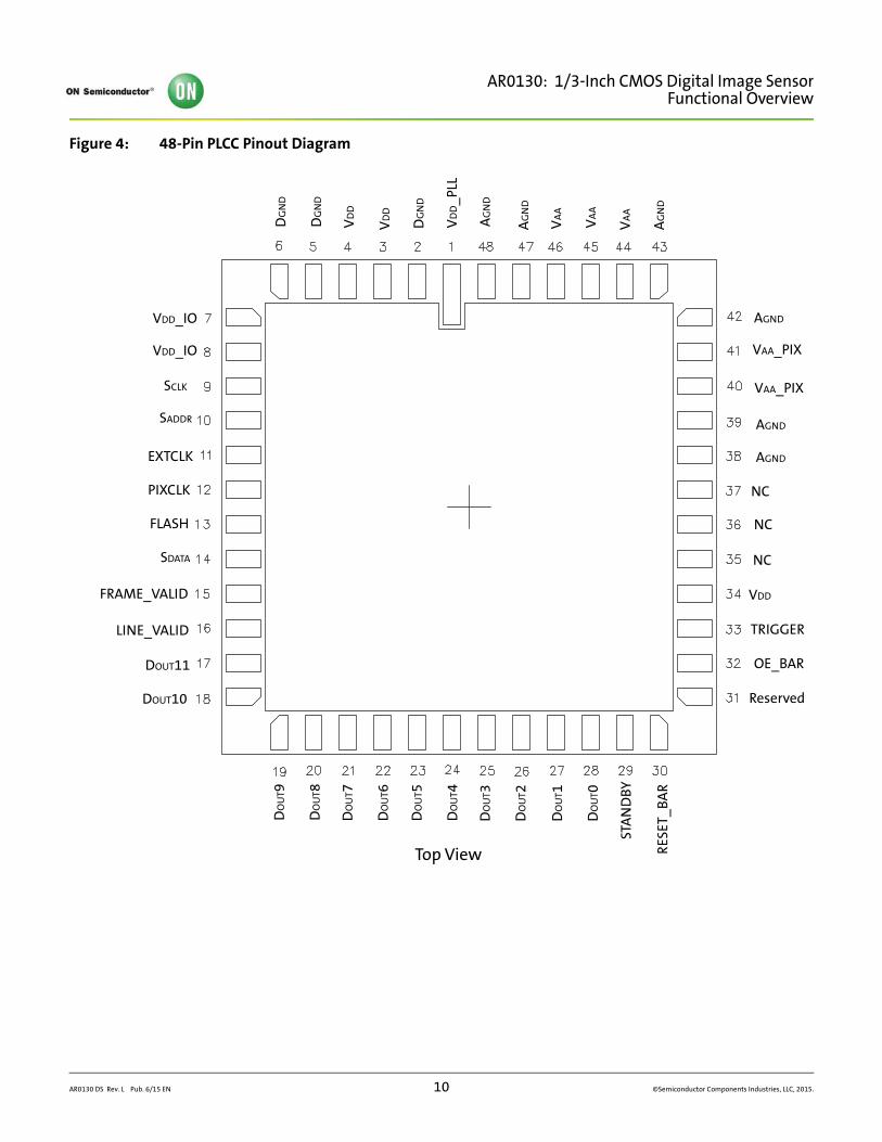
Figure 4: 48-Pin PLCC Pinout Diagram
Top View
Reserved
OE_BAR
NC
NC
NC
RESE
T_BA
R
VDD_IO
VDD_IO
VDD
VD
D_P
LL
VD
D
VD
DVAA_PIX
VAA_PIX
VA
A
VA
A
VA
A
SCLK
SADDR
SDATA
DG
ND
DG
ND
DG
ND
AG
ND
AG
ND
AG
ND
AGND
AGND
AGND
DO
UT9
DO
UT8
DO
UT7
DO
UT6
DO
UT5
DO
UT4
DO
UT3
DO
UT2
DO
UT1
DO
UT0
DOUT11
DOUT10
TRIGGER
EXTCLK
PIXCLK
FLASH
FRAME_VALID
LINE_VALIDST
AN
DBY
AR0130 DS Rev. L Pub. 6/15 EN 10 ©Semiconductor Components Industries, LLC, 2015.
AR0130: 1/3-Inch CMOS Digital Image SensorPixel Data Format
Pixel Data Format
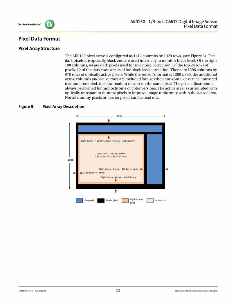
Pixel Array Structure
The AR0130 pixel array is configured as 1412 columns by 1028 rows, (see Figure 5). The dark pixels are optically black and are used internally to monitor black level. Of the right 108 columns, 64 are dark pixels used for row noise correction. Of the top 24 rows of pixels, 12 of the dark rows are used for black level correction. There are 1296 columns by 976 rows of optically active pixels. While the sensor's format is 1280 x 960, the additional active columns and active rows are included for use when horizontal or vertical mirrored readout is enabled, to allow readout to start on the same pixel. The pixel adjustment is always performed for monochrome or color versions. The active area is surrounded with optically transparent dummy pixels to improve image uniformity within the active area. Not all dummy pixels or barrier pixels can be read out.
Figure 5: Pixel Array Description
2 light dummy + 4 barrier + 24 dark + 4 barrier + 6 dark dummy
Dark pixel Barrier pixel Light dummy pixel
Active pixel
2 light dummy + 4 barrier + 6 dark dummy
1412
2 light dummy + 4 barrier
2 light dummy + 4 barrier + 100 dark + 4 barrier
1028
1296 x 976 (1288 x 968 active)4.86 x 3.66 mm2 (4.83 x 3.63 mm2)
AR0130 DS Rev. L Pub. 6/15 EN 11 ©Semiconductor Components Industries, LLC, 2015.
AR0130: 1/3-Inch CMOS Digital Image SensorPixel Data Format
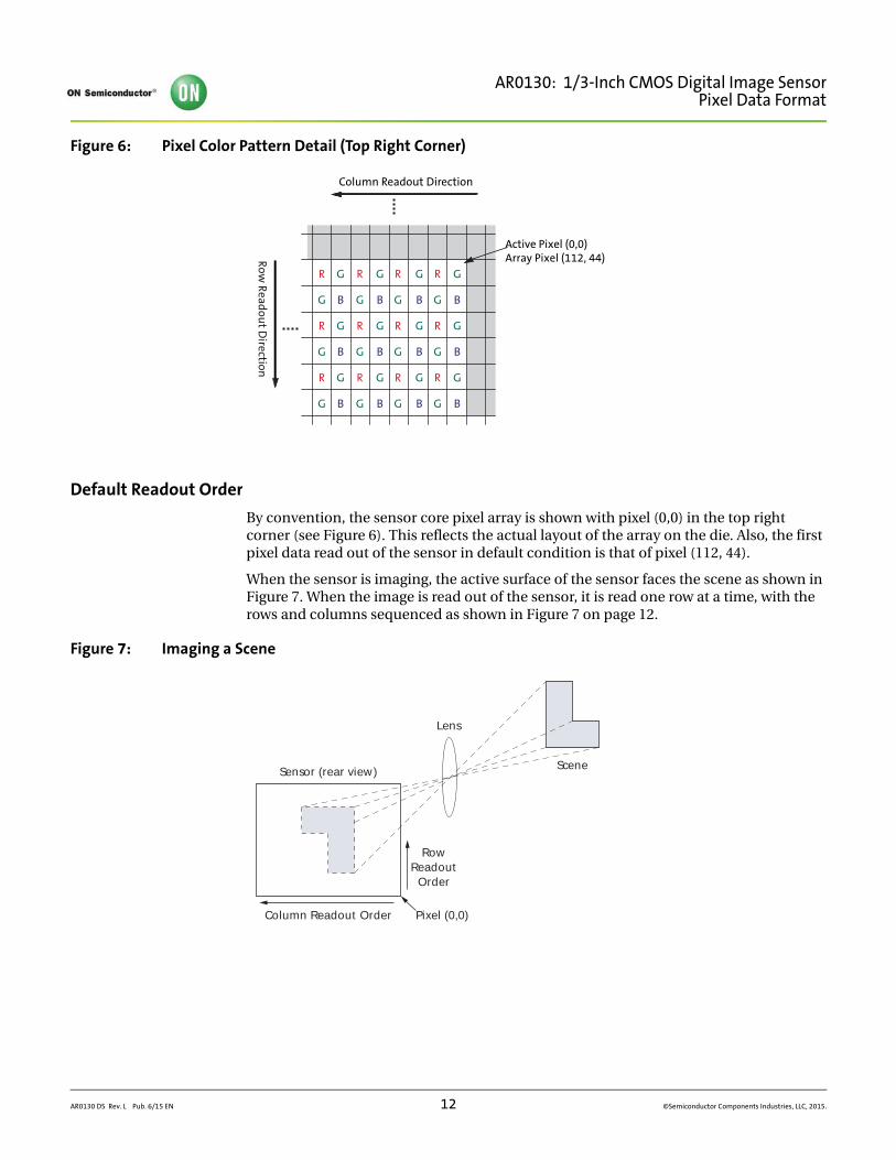
Figure 6: Pixel Color Pattern Detail (Top Right Corner)
Default Readout Order
By convention, the sensor core pixel array is shown with pixel (0,0) in the top right corner (see Figure 6). This reflects the actual layout of the array on the die. Also, the first pixel data read out of the sensor in default condition is that of pixel (112, 44).
When the sensor is imaging, the active surface of the sensor faces the scene as shown in Figure 7. When the image is read out of the sensor, it is read one row at a time, with the rows and columns sequenced as shown in Figure 7 on page 12.
Figure 7: Imaging a Scene
Active Pixel (0,0)Array Pixel (112, 44)Row
Readout D
irection
G
B
G
B
G
B
R
G
R
G
R
G
R
G
R
G
R
G
R
G
R
G
R
G
R
G
R
G
R
G
G
B
G
B
G
B
G
B
G
B
G
B
G
B
G
B
G
B
Column Readout Direction
Lens
Pixel (0,0)
RowReadout
Order
Column Readout Order
SceneSensor (rear view)
AR0130 DS Rev. L Pub. 6/15 EN 12 ©Semiconductor Components Industries, LLC, 2015.
AR0130: 1/3-Inch CMOS Digital Image SensorOutput Data Format
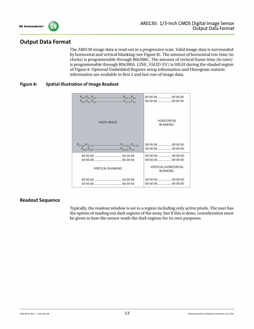
Output Data FormatThe AR0130 image data is read out in a progressive scan. Valid image data is surrounded by horizontal and vertical blanking (see Figure 8). The amount of horizontal row time (in clocks) is programmable through R0x300C. The amount of vertical frame time (in rows) is programmable through R0x300A. LINE_VALID (LV) is HIGH during the shaded region of Figure 8. Optional Embedded Register setup information and Histogram statistic information are available in first 2 and last row of image data.
Figure 8: Spatial Illustration of Image Readout
Readout Sequence
Typically, the readout window is set to a region including only active pixels. The user has the option of reading out dark regions of the array, but if this is done, consideration must be given to how the sensor reads the dark regions for its own purposes.
P0,0 P0,1 P0,2.....................................P0,n-1 P0,nP1,0 P1,1 P1,2.....................................P1,n-1 P1,n
00 00 00 .................. 00 00 0000 00 00 .................. 00 00 00
Pm-1,0 Pm-1,1.....................................Pm-1,n-1 Pm-1,nPm,0 Pm,1.....................................Pm,n-1 Pm,n
00 00 00 .................. 00 00 0000 00 00 .................. 00 00 00
00 00 00 .................. 00 00 0000 00 00 .................. 00 00 00
00 00 00 .................. 00 00 0000 00 00 .................. 00 00 00
00 00 00 ..................................... 00 00 0000 00 00 ..................................... 00 00 00
00 00 00 ..................................... 00 00 0000 00 00 ..................................... 00 00 00
VALID IMAGE HORIZONTALBLANKING
VERTICAL BLANKING VERTICAL/HORIZONTALBLANKING
AR0130 DS Rev. L Pub. 6/15 EN 13 ©Semiconductor Components Industries, LLC, 2015.
AR0130: 1/3-Inch CMOS Digital Image SensorOutput Data Format
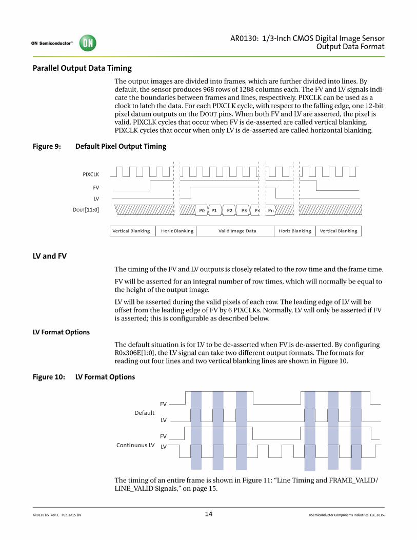
Parallel Output Data Timing
The output images are divided into frames, which are further divided into lines. By default, the sensor produces 968 rows of 1288 columns each. The FV and LV signals indi-cate the boundaries between frames and lines, respectively. PIXCLK can be used as a clock to latch the data. For each PIXCLK cycle, with respect to the falling edge, one 12-bit pixel datum outputs on the DOUT pins. When both FV and LV are asserted, the pixel is valid. PIXCLK cycles that occur when FV is de-asserted are called vertical blanking. PIXCLK cycles that occur when only LV is de-asserted are called horizontal blanking.
Figure 9: Default Pixel Output Timing
LV and FV
The timing of the FV and LV outputs is closely related to the row time and the frame time.
FV will be asserted for an integral number of row times, which will normally be equal to the height of the output image.
LV will be asserted during the valid pixels of each row. The leading edge of LV will be offset from the leading edge of FV by 6 PIXCLKs. Normally, LV will only be asserted if FV is asserted; this is configurable as described below.
LV Format Options
The default situation is for LV to be de-asserted when FV is de-asserted. By configuring R0x306E[1:0], the LV signal can take two different output formats. The formats for reading out four lines and two vertical blanking lines are shown in Figure 10.
Figure 10: LV Format Options
The timing of an entire frame is shown in Figure 11: “Line Timing and FRAME_VALID/LINE_VALID Signals,” on page 15.
PIXCLK
FV
LV
DOUT[11:0] P0 P1 P2 P3 P4 Pn
Vertical Blanking Horiz Blanking Valid Image Data Horiz Blanking Vertical Blanking
Default
Continuous LV
FV
LV
FV
LV
AR0130 DS Rev. L Pub. 6/15 EN 14 ©Semiconductor Components Industries, LLC, 2015.
AR0130: 1/3-Inch CMOS Digital Image SensorOutput Data Format
Frame Time
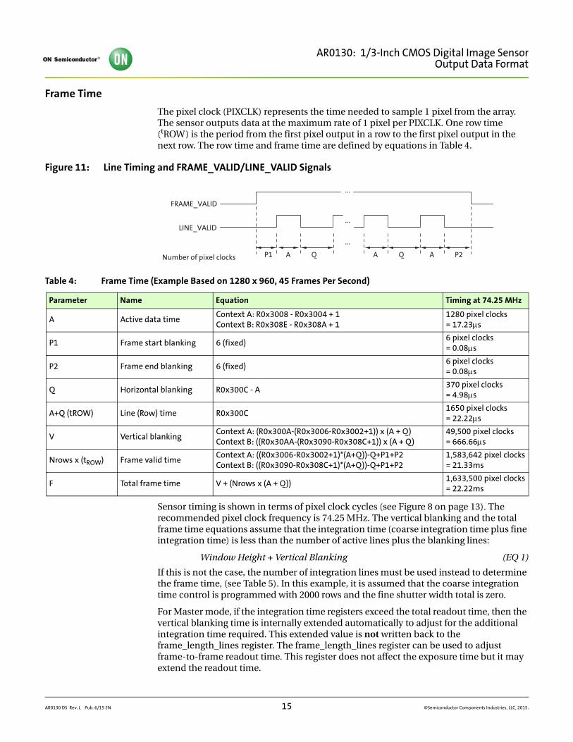
The pixel clock (PIXCLK) represents the time needed to sample 1 pixel from the array. The sensor outputs data at the maximum rate of 1 pixel per PIXCLK. One row time (tROW) is the period from the first pixel output in a row to the first pixel output in the next row. The row time and frame time are defined by equations in Table 4.
Figure 11: Line Timing and FRAME_VALID/LINE_VALID Signals
Sensor timing is shown in terms of pixel clock cycles (see Figure 8 on page 13). The recommended pixel clock frequency is 74.25 MHz. The vertical blanking and the total frame time equations assume that the integration time (coarse integration time plus fine integration time) is less than the number of active lines plus the blanking lines:
Window Height + Vertical Blanking (EQ 1)
If this is not the case, the number of integration lines must be used instead to determine the frame time, (see Table 5). In this example, it is assumed that the coarse integration time control is programmed with 2000 rows and the fine shutter width total is zero.
For Master mode, if the integration time registers exceed the total readout time, then the vertical blanking time is internally extended automatically to adjust for the additional integration time required. This extended value is not written back to the frame_length_lines register. The frame_length_lines register can be used to adjust frame-to-frame readout time. This register does not affect the exposure time but it may extend the readout time.
Table 4: Frame Time (Example Based on 1280 x 960, 45 Frames Per Second)
Parameter Name Equation Timing at 74.25 MHz
A Active data timeContext A: R0x3008 - R0x3004 + 1Context B: R0x308E - R0x308A + 1
1280 pixel clocks= 17.23s
P1 Frame start blanking 6 (fixed)6 pixel clocks= 0.08s
P2 Frame end blanking 6 (fixed)6 pixel clocks= 0.08s
Q Horizontal blanking R0x300C - A370 pixel clocks= 4.98s
A+Q (tROW) Line (Row) time R0x300C1650 pixel clocks = 22.22s
V Vertical blankingContext A: (R0x300A-(R0x3006-R0x3002+1)) x (A + Q)Context B: ((R0x30AA-(R0x3090-R0x308C+1)) x (A + Q)
49,500 pixel clocks= 666.66s
Nrows x (tROW) Frame valid timeContext A: ((R0x3006-R0x3002+1)*(A+Q))-Q+P1+P2Context B: ((R0x3090-R0x308C+1)*(A+Q))-Q+P1+P2
1,583,642 pixel clocks= 21.33ms
F Total frame time V + (Nrows x (A + Q))1,633,500 pixel clocks= 22.22ms
P1 A Q A Q A P2Number of pixel clocks
FRAME_VALID
LINE_VALID
...
...
...
AR0130 DS Rev. L Pub. 6/15 EN 15 ©Semiconductor Components Industries, LLC, 2015.
AR0130: 1/3-Inch CMOS Digital Image SensorOutput Data Format
Note: The AR0130 uses column parallel analog-digital converters; thus short line timing is not possible. The minimum total line time is 1390 columns (horizontal width + horizontal blanking). The mini-mum horizontal blanking is 110.
Exposure
Total integration time is the result of Coarse_Integration_Time and Fine_Integration_-Time registers, and depends also on whether manual or automatic exposure is selected.
The actual total integration time, tINT is defined as:
tINT = tINTCoarse - 410 - tINTFine (EQ 2)
= (number of lines of integration x line time) - (410 pixel clocks of conversion time over-head) - (number of pixels of integration x pixel time)
where:– Number of Lines of Integration (Auto Exposure Control: Enabled)
When automatic exposure control (AEC) is enabled, the number of lines of integra-tion may vary from frame to frame, with the limits controlled by R0x311E (mini-mum auto exposure time) and R0x311C (maximum auto exposure time).
– Number of Lines of Integration (Auto Exposure Control: Disabled)If AEC is disabled, the number of lines of integration equals the value in R0x3012 (context A) or R0x3016 (context B).
– Number of Pixels of IntegrationThe number of fine shutter width pixels is independent of AEC mode (enabled or disabled):• Context A: the number of pixels of integration equals the value in R0x3014.• Context B: the number of pixels of integration equals the value in R0x3018.
Typically, the value of the Coarse_Integration_Time register is limited to the number of lines per frame (which includes vertical blanking lines), such that the frame rate is not affected by the integration time. For more information on coarse and fine integration time settings limits, please refer to the Register Reference document.
Table 5: Frame Time: Long Integration Time
Parameter NameEquation(Number of Pixel Clock Cycles)
Default Timingat 74.25 MHz
F’Total frame time (long integration time)
Context A: (R0x3012 x (A + Q)) + R0x3014 + P1 + P2Context B: (R0x3016 x (A + Q)) + V R0x3018 + P1 + P2
3,300,012 pixel clocks= 44.44ms
AR0130 DS Rev. L Pub. 6/15 EN 16 ©Semiconductor Components Industries, LLC, 2015.
AR0130: 1/3-Inch CMOS Digital Image SensorReal-Time Context Switching
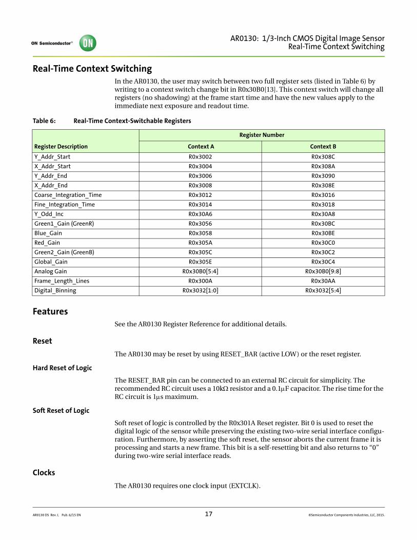
Real-Time Context SwitchingIn the AR0130, the user may switch between two full register sets (listed in Table 6) by writing to a context switch change bit in R0x30B0[13]. This context switch will change all registers (no shadowing) at the frame start time and have the new values apply to the immediate next exposure and readout time.
FeaturesSee the AR0130 Register Reference for additional details.
Reset
The AR0130 may be reset by using RESET_BAR (active LOW) or the reset register.
Hard Reset of Logic
The RESET_BAR pin can be connected to an external RC circuit for simplicity. The recommended RC circuit uses a 10k resistor and a 0.1F capacitor. The rise time for the RC circuit is 1s maximum.
Soft Reset of Logic
Soft reset of logic is controlled by the R0x301A Reset register. Bit 0 is used to reset the digital logic of the sensor while preserving the existing two-wire serial interface configu-ration. Furthermore, by asserting the soft reset, the sensor aborts the current frame it is processing and starts a new frame. This bit is a self-resetting bit and also returns to “0” during two-wire serial interface reads.
Clocks
The AR0130 requires one clock input (EXTCLK).
Table 6: Real-Time Context-Switchable Registers
Register Description
Register Number
Context A Context B
Y_Addr_Start R0x3002 R0x308C
X_Addr_Start R0x3004 R0x308A
Y_Addr_End R0x3006 R0x3090
X_Addr_End R0x3008 R0x308E
Coarse_Integration_Time R0x3012 R0x3016
Fine_Integration_Time R0x3014 R0x3018
Y_Odd_Inc R0x30A6 R0x30A8
Green1_Gain (GreenR) R0x3056 R0x30BC
Blue_Gain R0x3058 R0x30BE
Red_Gain R0x305A R0x30C0
Green2_Gain (GreenB) R0x305C R0x30C2
Global_Gain R0x305E R0x30C4
Analog Gain R0x30B0[5:4] R0x30B0[9:8]
Frame_Length_Lines R0x300A R0x30AA
Digital_Binning R0x3032[1:0] R0x3032[5:4]
AR0130 DS Rev. L Pub. 6/15 EN 17 ©Semiconductor Components Industries, LLC, 2015.
AR0130: 1/3-Inch CMOS Digital Image SensorFeatures
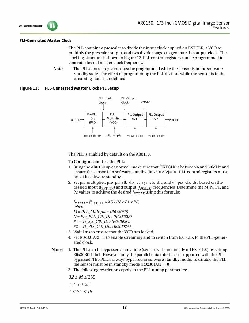
PLL-Generated Master Clock
The PLL contains a prescaler to divide the input clock applied on EXTCLK, a VCO to multiply the prescaler output, and two divider stages to generate the output clock. The clocking structure is shown in Figure 12. PLL control registers can be programmed to generate desired master clock frequency.
Note: The PLL control registers must be programmed while the sensor is in the software Standby state. The effect of programming the PLL divisors while the sensor is in the streaming state is undefined.
Figure 12: PLL-Generated Master Clock PLL Setup
The PLL is enabled by default on the AR0130.
To Configure and Use the PLL:1. Bring the AR0130 up as normal; make sure that fEXTCLK is between 6 and 50MHz and
ensure the sensor is in software standby (R0x301A[2]= 0). PLL control registers must be set in software standby.
2. Set pll_multiplier, pre_pll_clk_div, vt_sys_clk_div, and vt_pix_clk_div based on the desired input (fEXTCLK) and output (fPIXCLK) frequencies. Determine the M, N, P1, and P2 values to achieve the desired fPIXCLK using this formula:
fPIXCLK= (fEXTCLK × M) / (N × P1 x P2)where M = PLL_Multiplier (R0x3030)N = Pre_PLL_Clk_Div (R0x302E)P1 = Vt_Sys_Clk_Div (R0x302C)P2 = Vt_PIX_Clk_Div (R0x302A)
3. Wait 1ms to ensure that the VCO has locked.4. Set R0x301A[2]=1 to enable streaming and to switch from EXTCLK to the PLL-gener-
ated clock.
Notes: 1. The PLL can be bypassed at any time (sensor will run directly off EXTCLK) by setting R0x30B0[14]=1. However, only the parallel data interface is supported with the PLL bypassed. The PLL is always bypassed in software standby mode. To disable the PLL, the sensor must be in standby mode (R0x301A[2] = 0)
2. The following restrictions apply to the PLL tuning parameters:
Pre PLL Div (PFD)
Pre_pll_clk_div
EXTCLK
PLL Multiplier (VCO)
PLL Output Div 1
SYSCLK
PIXCLK
vt_pix_clk_div vt_sys_clk_div
PLL Input
Clock
PLL Output Clock
PLL Output Div 2
pll_multiplier
32 M 255 1 N 63 1 P1 16
AR0130 DS Rev. L Pub. 6/15 EN 18 ©Semiconductor Components Industries, LLC, 2015.
AR0130: 1/3-Inch CMOS Digital Image SensorFeatures
Additionally, the VCO frequency, defined as must be within384-768MHz and the EXTCLK must be within 2MHz =< fEXTCLK /N <= 24MHz
The user can utilize the Register Wizard tool accompanying DevWare to generate PLL settings given a supplied input clock and desired output frequency.
Spread-Spectrum Clocking
To facilitate improved EMI performance, the external clock input allows for spread spec-trum sources, with no impact on image quality. Limits of the spread spectrum input clock are:• 5% maximum clock modulation• 35 KHz maximum modulation frequency• Accepts triangle wave modulation, as well as sine or modified triangle modulations.
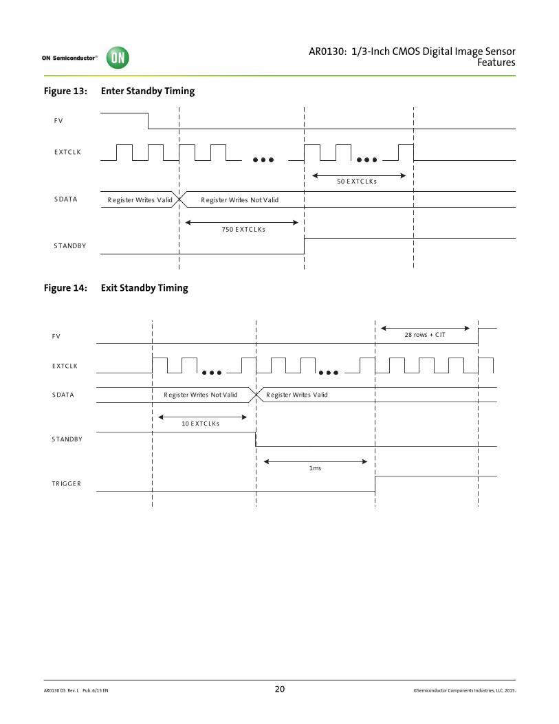
Stream/Standby Control
The sensor supports two standby modes: Hard Standby and Soft Standby. In both modes, external clock can be optionally disabled to further minimize power consump-tion. If this is done, then the “Power-Up Sequence” on page 48 must be followed.
Soft Standby
Soft Standby is a low power state that is controlled through register R0x301A[2]. Depending on the value of R0x301A[4], the sensor will go to standby after completion of the current frame readout (default behavior) or after the completion of the current row readout. When the sensor comes back from Soft Standby, previously written register settings are still maintained.
A specific sequence needs to be followed to enter and exit from Soft Standby.
To Enter Soft Standby:1. R0x301A[12] = 1 if serial mode was used2. Set R0x301A[2] = 03. External clock can be turned off to further minimize power consumption (Optional)
To Exit Soft Standby:1. Enable external clock if it was turned off2. R0x301A[2] = 13. R0x301A[12] = 0 if serial mode is used
4 P2 16 fVCO fEXTCLK M N=
AR0130 DS Rev. L Pub. 6/15 EN 19 ©Semiconductor Components Industries, LLC, 2015.
AR0130: 1/3-Inch CMOS Digital Image SensorFeatures
Figure 13: Enter Standby Timing
Figure 14: Exit Standby Timing
E XTC L K
S TANDBY
F V
50 E XTC L Ks
R egister Writes Not ValidR egister Writes ValidS DATA
750 E XTC L Ks
E XTC L K
S TANDBY
F V
TR IGGE R
10 E XTC L Ks
1ms
28 rows + C IT
R egister Writes Not Valid R egister Writes ValidS DATA
AR0130 DS Rev. L Pub. 6/15 EN 20 ©Semiconductor Components Industries, LLC, 2015.
AR0130: 1/3-Inch CMOS Digital Image SensorFeatures
Hard Standby
Hard Standby puts the sensor in lower power state; previously written register settings are still maintained.
A specific sequence needs to be followed to enter and exit from Hard Standby.
To Enter Hard Standby:1. R0x301A[8] = 12. R0x301A[12] = 1 if serial mode was used3. Assert STANDBY pin 4. External clock can be turned off to further minimize power consumption (Optional)
To Exit Hard Standby:1. Enable external clock if it was turned off2. De-assert STANDBY pin3. Set R0x301A[8] = 0
Window Control
Registers x_addr_start, x_addr_end, y_addr_start, and y_addr_end control the size and starting coordinates of the image window.
The exact window height and width out of the sensor is determined by the difference between the Y address start and end registers or the X address start and end registers, respectively.
The AR0130 allows different window sizes for context A and context B.
Blanking Control
Horizontal blank and vertical blank times are controlled by the line_length_pck and frame_length_lines registers, respectively.• Horizontal blanking is specified in terms of pixel clocks. It is calculated by subtracting
the X window size from the line_length_pck register. The minimum horizontal blanking is 110 pixel clocks.
• Vertical blanking is specified in terms of numbers of lines. It is calculated by subtracting the Y window size from the frame_length_lines register. The minimum vertical blanking is 26 lines.
The actual imager timing can be calculated using Table 4 on page 15 and Table 5 on page 16, which describe the Line Timing and FV/LV signals.
AR0130 DS Rev. L Pub. 6/15 EN 21 ©Semiconductor Components Industries, LLC, 2015.
AR0130: 1/3-Inch CMOS Digital Image SensorFeatures
Readout Modes
Digital Binning
By default, the resolution of the output image is the full width and height of the FOV as defined above. The output resolution can be reduced by digital binning. For RGB and monochrome mode, this is set by the register R0x3032. For Context A, use bits [1:0], for Context B, use bits [5:4]. Available settings are:
00 = No binning
01 = Horizontal binning
10 = Horizontal and vertical binning
Binning gives the advantage of reducing noise at the cost of reduced resolution. When both horizontal and vertical binning are used, a 2x improvement in SNR is achieved therefore improving low light performance
Bayer Space Resampling
All of the pixels in the FOV contribute to the output image in digital binning mode. This can result in a more pleasing output image with reduced subsampling artifacts. It also improves low-light performance. For RGB mode, resampling can be enabled by setting of register 0x306E[4] = 1.
Mirror
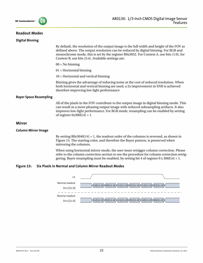
Column Mirror Image
By setting R0x3040[14] = 1, the readout order of the columns is reversed, as shown in Figure 15. The starting color, and therefore the Bayer pattern, is preserved when mirroring the columns.
When using horizontal mirror mode, the user must retrigger column correction. Please refer to the column correction section to see the procedure for column correction retrig-gering. Bayer resampling must be enabled, by setting bit 4 of register 0 x 306E[4] = 1.
Figure 15: Six Pixels in Normal and Column Mirror Readout Modes
G0[11:0] R0[11:0] G1[11:0] R1[11:0] G2[11:0] R2[11:0]
G2[11:0] R2[11:0] G1[11:0] R1[11:0] G0[11:0] R0[11:0]
DOUT[11:0]
LV
Normal readout
DOUT[11:0]
Reverse readout
AR0130 DS Rev. L Pub. 6/15 EN 22 ©Semiconductor Components Industries, LLC, 2015.
AR0130: 1/3-Inch CMOS Digital Image SensorFeatures
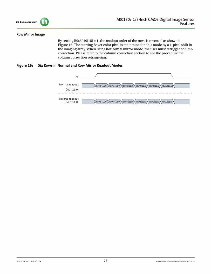
Row Mirror Image
By setting R0x3040[15] = 1, the readout order of the rows is reversed as shown in Figure 16. The starting Bayer color pixel is maintained in this mode by a 1-pixel shift in the imaging array. When using horizontal mirror mode, the user must retrigger column correction. Please refer to the column correction section to see the procedure for column correction retriggering.
Figure 16: Six Rows in Normal and Row Mirror Readout Modes
Row0 [11:0] Row1 [11:0] Row2 [11:0] Row3 [11:0] Row4 [11:0] Row5 [11:0]
Row5 [11:0] Row4 [11:0] Row3 [11:0] Row2 [11:0] Row1 [11:0] Row0[11:0]
DOUT[11:0]
FV
Normal readout
DOUT[11:0]Reverse readout
AR0130 DS Rev. L Pub. 6/15 EN 23 ©Semiconductor Components Industries, LLC, 2015.
AR0130: 1/3-Inch CMOS Digital Image SensorFeatures
Maintaining a Constant Frame Rate
Maintaining a constant frame rate while continuing to have the ability to adjust certain parameters is the desired scenario. This is not always possible, however, because register updates are synchronized to the read pointer, and the shutter pointer for a frame is usually active during the readout of the previous frame. Therefore, any register changes that could affect the row time or the set of rows sampled causes the shutter pointer to start over at the beginning of the next frame.
By default, the following register fields cause a “bubble” in the output rate (that is, the vertical blank increases for one frame) if they are written in video mode, even if the new value would not change the resulting frame rate. The following list shows only a few examples of such registers; a full listing can be seen in the AR0130 Register Reference.• x_addr_start • x_addr_end • y_addr_start • y_addr_end • frame_length_lines• line_length_pclk• coarse_integration_time• fine_integration_time• read_mode
The size of this bubble is (Integration_Time × tROW), calculating the row time according to the new settings.
The Coarse_Integration_Time and Fine_Integration_Time fields may be written to without causing a bubble in the output rate under certain circumstances. Because the shutter sequence for the next frame often is active during the output of the current frame, this would not be possible without special provisions in the hardware. Writes to these registers take effect two frames after the frame they are written, which allows the integration time to increase without interrupting the output or producing a corrupt frame (as long as the change in integration time does not affect the frame time).
Synchronizing Register Writes to Frame Boundaries
Changes to most register fields that affect the size or brightness of an image take effect on the frame after the one during which they are written. These fields are noted as “synchronized to frame boundaries” in the AR0130 Register Reference. To ensure that a register update takes effect on the next frame, the write operation must be completed after the leading edge of FV and before the trailing edge of FV.
As a special case, in single frame mode, register writes that occur after FV but before the next trigger will take effect immediately on the next frame, as if there had been a Restart. However, if the trigger for the next frame occurs during FV, register writes take effect as with video mode.
Fields not identified as being frame-synchronized are updated immediately after the register write is completed. The effect of these registers on the next frame can be difficult to predict if they affect the shutter pointer.
AR0130 DS Rev. L Pub. 6/15 EN 24 ©Semiconductor Components Industries, LLC, 2015.
AR0130: 1/3-Inch CMOS Digital Image SensorFeatures
Restart
To restart the AR0130 at any time during the operation of the sensor, write a “1” to the Restart register (R0x301A[1] = 1). This has two effects: first, the current frame is inter-rupted immediately. Second, any writes to frame-synchronized registers and the shutter width registers take effect immediately, and a new frame starts (in video mode). The current row completes before the new frame is started, so the time between issuing the Restart and the beginning of the next frame can vary by about tROW.
Image Acquisition Modes
The AR0130 supports two image acquisition modes: video (also known as master) and single frame.
Video
The video mode takes pictures by scanning the rows of the sensor twice. On the first scan, each row is released from reset, starting the exposure. On the second scan, the row is sampled, processed, and returned to the reset state. The exposure for any row is there-fore the time between the first and second scans. Each row is exposed for the same dura-tion, but at slightly different point in time, which can cause a shear in moving subjects as is typical with electronic rolling shutter sensors.
Single Frame
The single-frame mode operates similar to the video mode. It also scans the rows of the sensor twice, first to reset the rows and second to read the rows. Unlike video mode where a continuous stream of images are output from the image sensor, the single-frame mode outputs a single frame in response to a high state placed on the TRIGGER input pin. As long as the TRIGGER pin is held in a high state, new images will be read out. After the TRIGGER pin is returned to a low state, the image sensor will not output any new images and will wait for the next high state on the TRIGGER pin.
The TRIGGER pin state is detected during the vertical blanking period (i.e. the FV signal is low). The pin is level sensitive rather than edge sensitive. As such, image integration will only begin when the sensor detects that the TRIGGER pin has been held high for 3 consecutive clock cycles.
During integration time of single-frame mode and video mode, the FLASH output pin is at high.
Continuous Trigger
In certain applications, multiple sensors need to have their video streams synchronized (E.g. surround view or panorama view applications). The TRIGGER pin can also be used to synchronize output of multiple image sensors together and still get a video stream. This is called continuous trigger mode. Continuous trigger is enabled by holding the TRIGGER pin high. Alternatively, the TRIGGER pin can be held high until the stream bit is enabled (R0x301A[2]=1) then can be released for continuous synchronized video streaming.
If the TRIGGER pins for all connected AR0130 sensors are connected to the same control signal, all sensors will receive the trigger pulse at the same time. If they are configured to have the same frame timing, then the usage of the TRIGGER pin guarantees that all sensors will be synchronized within 1 PIXCLK cycle if PLL is disabled, or 2 PIXCLK cycles if PLL is enabled.
AR0130 DS Rev. L Pub. 6/15 EN 25 ©Semiconductor Components Industries, LLC, 2015.
AR0130: 1/3-Inch CMOS Digital Image SensorFeatures
With continuous trigger mode, the application can now make use of the video streaming mode while guaranteeing that all sensor outputs are synchronized. As long as the initial trigger for the sensors takes place at the same time, all subsequent video streams will be synchronous.
Automatic Exposure Control
The integrated automatic exposure control (AEC) is responsible for ensuring that optimal settings of exposure and gain are computed and updated every other frame. AEC can be enabled or disabled by R0x3100[0].
When AEC is disabled (R0x3100[0] = 0), the sensor uses the manual exposure value in coarse and fine shutter width registers and the manual gain value in the gain registers.
When AEC is enabled (R0x3100[0]=1), the target luma value is set by R0x3102. For the AR0130 this target luma has a default value of 0x0800 or about half scale.
The exposure control measures current scene luminosity by accumulating a histogram of pixel values while reading out a frame. It then compares the current luminosity to the desired output luminosity. Finally, the appropriate adjustments are made to the expo-sure time and gain. All pixels are used, regardless of color or mono mode.
AEC does not work if digital binning is enabled.
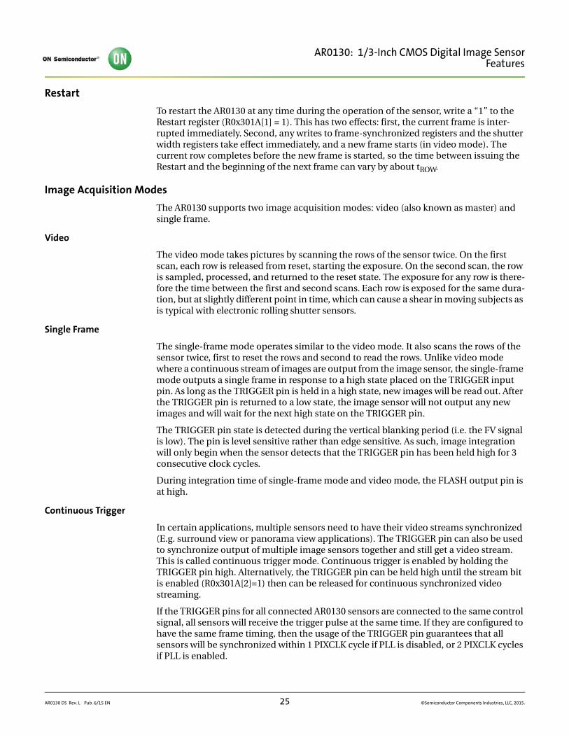
Embedded Data and Statistics
The AR0130 has the capability to output image data and statistics embedded within the frame timing. There are two types of information embedded within the frame readout: 1. Embedded Data: If enabled, these are displayed on the two rows immediately before
the first active pixel row is displayed. 2. Embedded Statistics: If enabled, these are displayed on the two rows immediately
after the last active pixel row is displayed.
Note: Both embedded statistics and data must be enabled and disabled together.
Figure 17: Frame Format with Embedded Data Lines Enabled
Image
Register Data
Status & Statistics Data
HBlank
VBlank
AR0130 DS Rev. L Pub. 6/15 EN 26 ©Semiconductor Components Industries, LLC, 2015.
AR0130: 1/3-Inch CMOS Digital Image SensorFeatures
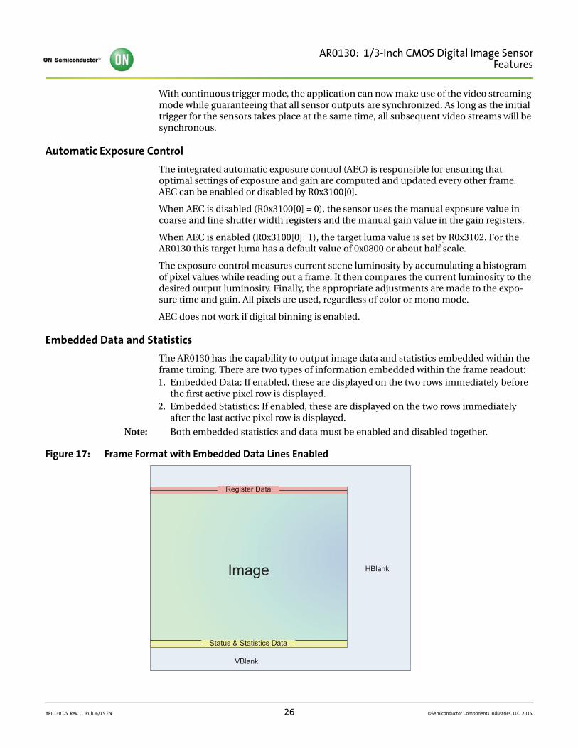
Embedded Data
The embedded data contains the configuration of the image being displayed. This includes all register settings used to capture the current frame. The registers embedded in these rows are as follows:
Line 1: Registers R0x3000 to R0x312F
Line 2: Registers R0x3136 to R0x31BF, R0x31D0 to R0x31FF
Note: All undefined registers will have a value of 0.
In parallel mode, since the pixel word depth is 12-bits/pixel, the sensor 16-bit register data will be transferred over 2 pixels where the register data will be broken up into 8 MSB and 8 LSB. The alignment of the 8-bit data will be on the 8 MSB bits of the 12-bit pixel word. For example, of a register value of 0x1234 is to be transmitted, it will be trans-mitted over 2, 12-bit pixels as follows: 0x120, 0x340.
The first pixel of each line in the embedded data is a tag value of 0x0A0. This signifies that all subsequent data is 8 bit data aligned to the MSB of the 12-bit pixel.
The figure below summarizes how the embedded data transmission looks like. It should be noted that data, as shown in Figure 18, is aligned to the MSB of each word:
Figure 18: Format of Embedded Data Output within a Frame
The data embedded in these rows are as follows:• 0x0A0 - identifier• 0xAA0• Register Address MSB of the first register• 0xA50• Register Address LSB of the first register• 0x5A0• Register Value MSB of the first register addressed• 0x5A0• Register Value LSB of the first register addressed• 0x5A0• Register Value MSB of the register at first address + 2• 0x5A0• Register Value LSB of the register at first address + 2• 0x5A0• etc.
{register_value_LSB} 8'h5A
Data line 1
Data line 2
8'h5A
8'hAA {register_address_MSB} 8'hA5
{register_address_LSB} 8'h5A
{register_value_MSB} 8'h5A
{register_value_LSB}
data_format_code =8'h0A
8'hAA{register_address_MSB}
8'hA5 {register_address_LSB}
8'h5A {register_value_MSB}
8'h5Adata_format_code =8'h0A
AR0130 DS Rev. L Pub. 6/15 EN 27 ©Semiconductor Components Industries, LLC, 2015.
AR0130: 1/3-Inch CMOS Digital Image SensorFeatures
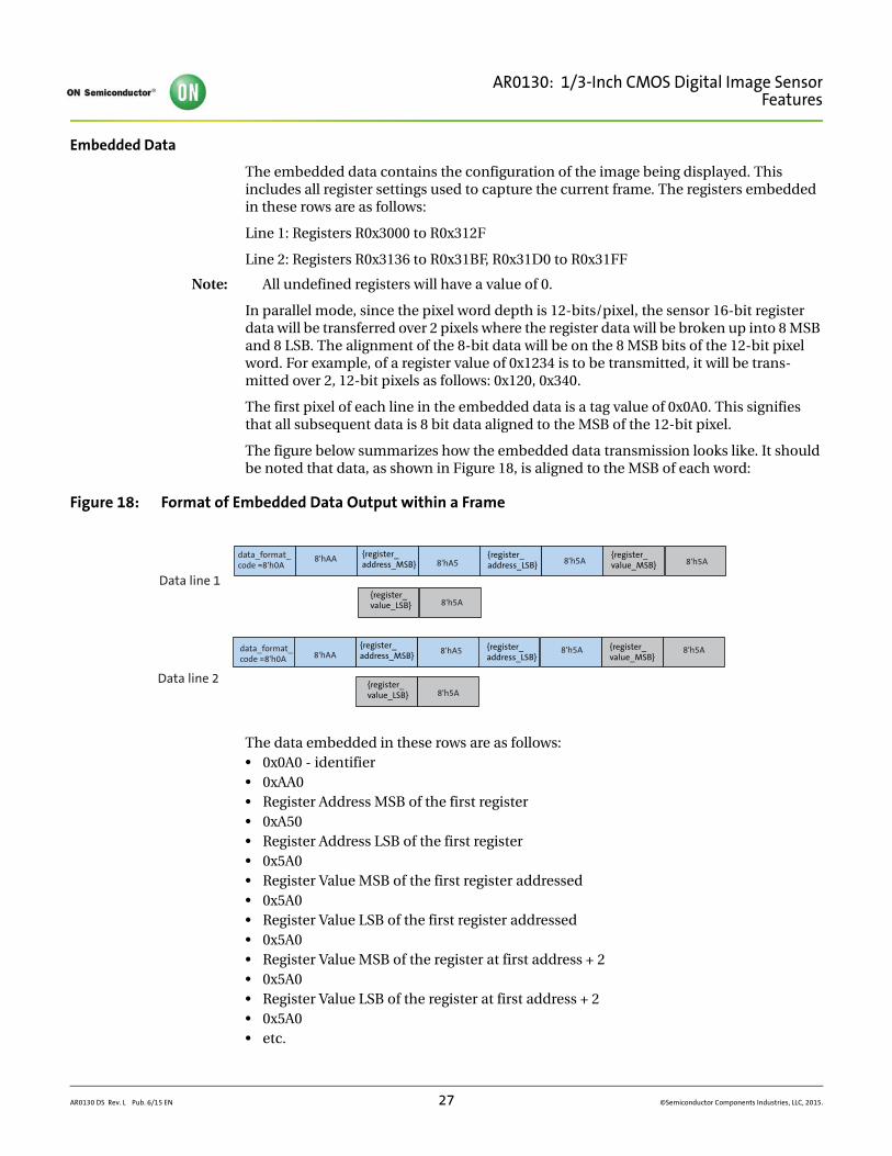
Embedded Statistics
The embedded statistics contain frame identifiers and histogram information of the image in the frame. This can be used by downstream auto-exposure algorithm blocks to make decisions about exposure adjustment.
This histogram is divided into 244 bins with a bin spacing of 64 evenly spaced bins for digital code values 0 to 212, 120 evenly spaced bins for values 212 to 216, 60 evenly spaced bins for values 216 to 220.
The first pixel of each line in the embedded statistics is a tag value of 0x0B0. This signi-fies that all subsequent statistics data is 10 bit data aligned to the MSB of the 12-bit pixel.
The figure below summarizes how the embedded statistics transmission looks like. It should be noted that data, as shown in Figure 19, is aligned to the msb of each word:
Figure 19: Format of Embedded Statistics Output within a Frame
The statistics embedded in these rows are as follows:
Line 1: • 0x0B0 - identifier • Register 0x303A - frame_count • Register 0x31D2 - frame ID • Histogram data - histogram bins 0-243
Line 2: • 0x0B0 (identifier) • Mean • Histogram Begin • Histogram End • Low End Histogram Mean • Percentage of Pixels Below Low End Mean • Normal Absolute Deviation
lowEndMean[19:10]
stats line 1
stats line 2
histogrambin1 [9:0]
#words =10’h1EC
{2’b00, frame _count MSB}
{2’b00, frame _ID MSB}
{2’b00, frame _ID LSB}
histogrambin0 [19:10]
histogrambin0 [9:0]
histogrambin1 [19:10]
data_format_code =8'h0B
#words =10’h1C
mean [ 19:10] mean [9:0]hist_begin
[19:10]hist_begin
[9:10]
8'h07
data_format_code =8'h0B
{2’b00, frame _count LSB}
8'h07histogrambin243 [19:10]
histogrambin243 [9:0]
8'h07
hist_end[19:10]
hist_end[9:10]
lowEndMean[9:0]
perc_lowEnd[19:10]
perc_lowEnd[9:0]
norm_abs_dev[19:10]
lnorm_abs_dev[9:0]
AR0130 DS Rev. L Pub. 6/15 EN 28 ©Semiconductor Components Industries, LLC, 2015.
AR0130: 1/3-Inch CMOS Digital Image SensorFeatures
Gain
Digital Gain
Digital gain can be controlled globally by R0x305E (Context A) or R0x30C4 (Context B). There are also registers that allow individual control over each Bayer color (GreenR, GreenB, Red, Blue).
The format for digital gain setting is xxx.yyyyy where 0b00100000 represents a 1x gain setting and 0b00110000 represents a 1.5x gain setting. The step size for yyyyy is 0.03125 while the step size for xxx is 1. Therefore to set a gain of 2.09375 one would set digital gain to 01000011.
Analog Gain
The AR0130 has a column parallel architecture and therefore has an Analog gain stage per column.
There are two stages of analog gain, the first stage can be set to 1x, 2x, 4x or 8x. This is can be set in R0x30B0[5:4](Context A) or R0x30B0[9:8] (Context B). The second stage is capable of setting an additional 1x or 1.25x gain which can be set in R0x3EE4[8].
This allows the maximum possible analog gain to be set to 10x.
Black Level Correction
Black level correction is handled automatically by the image sensor. No adjustments are provided except to enable or disable this feature. Setting R0x30EA[15] disables the auto-matic black level correction. Default setting is for automatic black level calibration to be enabled.
The automatic black level correction measures the average value of pixels from a set of optically black lines in the image sensor. The pixels are averaged as if they were light-sensitive and passed through the appropriate gain. This line average is then digitally low-pass filtered over many frames to remove temporal noise and random instabilities associated with this measurement. The new filtered average is then compared to a minimum acceptable level, low threshold, and a maximum acceptable level, high threshold. If the average is lower than the minimum acceptable level, the offset correc-tion value is increased by a predetermined amount. If it is above the maximum level, the offset correction value is decreased by a predetermined amount. The high and low thresholds have been calculated to avoid oscillation of the black level from below to above the targeted black level. At high gain, long exposure, and high temperature condi-tions, the performance of this function can degrade.
Row-wise Noise Correction
Row (Line)-wise Noise Correction is handled automatically by the image sensor. No adjustments are provided except to enable or disable this feature. Clearing R0x3044[10] disables the row noise correction. Default setting is for row noise correction to be enabled.
Row-wise noise correction is performed by calculating an average from a set of optically black pixels at the start of each line and then applying each average to all the active pixels of the line.
AR0130 DS Rev. L Pub. 6/15 EN 29 ©Semiconductor Components Industries, LLC, 2015.
AR0130: 1/3-Inch CMOS Digital Image SensorFeatures
Column Correction
The AR0130 uses column parallel readout architecture to achieve fast frame rate. Without any corrections, the consequence of this architecture is that different column signal paths have slightly different offsets that might show up on the final image as structured fixed pattern noise.
AR0130 has column correction circuitry that measures this offset and removes it from the image before output. This is done by sampling dark rows containing tied pixels and measuring an offset coefficient per column to be corrected later in the signal path.
Column correction can be enabled/disabled via R0x30D4[15]. Additionally, the number of rows used for this offset coefficient measurement is set in R0x30D4[3:0]. By default this register is set to 0x7, which means that 8 rows are used. This is the recommended value. Other control features regarding column correction can be viewed in the AR0130 Register reference. Any changes to column correction settings need to be done when the sensor streaming is disabled and the appropriate triggering sequence must be followed as described below.
Column Correction Triggering
Column correction requires a special procedure to trigger depending on which state the sensor is in.
Column Triggering on Startup
When streaming the sensor for the first time after power-up, a special sequence needs to be followed to make sure that the column correction coefficients are internally calcu-lated properly. 1. Follow proper power up sequence for power supplies and clocks2. Apply sequencer settings if needed3. Apply frame timing and PLL settings as required by application4. Set analog gain to 1x and low conversion gain5. Enable column correction and settings6. Disable auto re-trigger for change in conversion gain or col_gain, and enable column
correction always. (R0x30BA = 0x0008).7. Enable streaming (R0x301A[2] = 1) or drive the TRIGGER pin HIGH.8. Wait 9 frames to settle. (First frame after coming up from standby is internally column
correction disabled.)9. Disable streaming (R0x301A[2] = 0) or drive the TRIGGER pin LOW.
After this, the sensor has calculated the proper column correction coefficients and the sensor is ready for streaming. Any other settings (including gain, integration time and conversion gain etc.) can be done afterwards without affecting column correction.
Column Correction Retriggering Due to Mode Change
Since column offsets is sensitive to changes in the analog signal path, such changes require column correction circuitry to be retriggered for the new path. Examples of such mode changes include: horizontal mirror, vertical mirror, changes to column correction settings.
When such changes take place, the following sequence needs to take place:1. Disable streaming (R0x301A[2]=0) or drive the TRIGGER pin LOW.2. Enable streaming (R0x301A[2]=1) or drive the TRIGGER pin HIGH.3. Wait 9 frames to settle.
AR0130 DS Rev. L Pub. 6/15 EN 30 ©Semiconductor Components Industries, LLC, 2015.
AR0130: 1/3-Inch CMOS Digital Image SensorFeatures
Note: The above steps are not needed if the sensor is being reset (soft or hard reset) upon the mode change.
Test Patterns
The AR0130 has the capability of injecting a number of test patterns into the top of the datapath to debug the digital logic. With one of the test patterns activated, any of the datapath functions can be enabled to exercise it in a deterministic fashion. Test patterns are selected by Test_Pattern_Mode register (R0x3070). Only one of the test patterns can be enabled at a given point in time by setting the Test_Pattern_Mode register according to Table 7. When test patterns are enabled the active area will receive the value specified by the selected test pattern and the dark pixels will receive the value in Test_Pat-tern_Green (R0x3074 and R0x3078) for green pixels, Test_Pattern_Blue (R0x3076) for blue pixels, and Test_Pattern_Red (R0x3072) for red pixels.
Note: Turn off black level calibration (BLC) when Test Pattern is enabled.
Color Field
When the color field mode is selected, the value for each pixel is determined by its color. Green pixels will receive the value in Test_Pattern_Green, red pixels will receive the value in Test_Pattern_Red, and blue pixels will receive the value in Test_Pattern_Blue.
Vertical Color Bars
When the vertical color bars mode is selected, a typical color bar pattern will be sent through the digital pipeline.
Walking 1s
When the walking 1s mode is selected, a walking 1s pattern will be sent through the digital pipeline. The first value in each row is 1.
Table 7: Test Pattern Modes
Test_Pattern_Mode Test Pattern Output
0 No test pattern (normal operation)
1 Solid color test pattern
2 100% color bar test pattern
3 Fade-to-gray color bar test pattern
256 Walking 1s test pattern (12-bit)
AR0130 DS Rev. L Pub. 6/15 EN 31 ©Semiconductor Components Industries, LLC, 2015.
AR0130: 1/3-Inch CMOS Digital Image SensorTwo-Wire Serial Register Interface
Two-Wire Serial Register InterfaceThe two-wire serial interface bus enables read/write access to control and status regis-ters within the AR0130. This interface is designed to be compatible with the electrical characteristics and transfer protocols of the two-wire serial interface specification.
The interface protocol uses a master/slave model in which a master controls one or more slave devices. The sensor acts as a slave device. The master generates a clock (SCLK) that is an input to the sensor and is used to synchronize transfers. Data is transferred between the master and the slave on a bidirectional signal (SDATA). SDATA is pulled up to VDD_IO off-chip by a 1.5k resistor. Either the slave or master device can drive SDATA LOW—the interface protocol determines which device is allowed to drive SDATA at any given time.
The protocols described in the two-wire serial interface specification allow the slave device to drive SCLK LOW; the AR0130 uses SCLK as an input only and therefore never drives it LOW.
Protocol
Data transfers on the two-wire serial interface bus are performed by a sequence of low-level protocol elements:1. a (repeated) start condition2. a slave address/data direction byte3. an (a no) acknowledge bit4. a message byte5. a stop condition
The bus is idle when both SCLK and SDATA are HIGH. Control of the bus is initiated with a start condition, and the bus is released with a stop condition. Only the master can generate the start and stop conditions.
Start Condition
A start condition is defined as a HIGH-to-LOW transition on SDATA while SCLK is HIGH. At the end of a transfer, the master can generate a start condition without previously generating a stop condition; this is known as a “repeated start” or “restart” condition.
Stop Condition
A stop condition is defined as a LOW-to-HIGH transition on SDATA while SCLK is HIGH.
Data Transfer
Data is transferred serially, 8 bits at a time, with the MSB transmitted first. Each byte of data is followed by an acknowledge bit or a no-acknowledge bit. This data transfer mechanism is used for the slave address/data direction byte and for message bytes.
One data bit is transferred during each SCLK clock period. SDATA can change when SCLK is LOW and must be stable while SCLK is HIGH.
Slave Address/Data Direction Byte
Bits [7:1] of this byte represent the device slave address and bit [0] indicates the data transfer direction. A “0” in bit [0] indicates a WRITE, and a “1” indicates a READ. The default slave addresses used by the AR0130 are 0x20 (write address) and 0x21 (read
AR0130 DS Rev. L Pub. 6/15 EN 32 ©Semiconductor Components Industries, LLC, 2015.
AR0130: 1/3-Inch CMOS Digital Image SensorTwo-Wire Serial Register Interface
address) in accordance with the specification. Alternate slave addresses of 0x30 (write address) and 0x31 (read address) can be selected by enabling and asserting the SADDR input.
An alternate slave address can also be programmed through R0x31FC.
Message Byte
Message bytes are used for sending register addresses and register write data to the slave device and for retrieving register read data.
Acknowledge Bit
Each 8-bit data transfer is followed by an acknowledge bit or a no-acknowledge bit in the SCLK clock period following the data transfer. The transmitter (which is the master when writing, or the slave when reading) releases SDATA. The receiver indicates an acknowl-edge bit by driving SDATA LOW. As for data transfers, SDATA can change when SCLK is LOW and must be stable while SCLK is HIGH.
No-Acknowledge Bit
The no-acknowledge bit is generated when the receiver does not drive SDATA LOW during the SCLK clock period following a data transfer. A no-acknowledge bit is used to terminate a read sequence.
Typical Sequence
A typical READ or WRITE sequence begins by the master generating a start condition on the bus. After the start condition, the master sends the 8-bit slave address/data direction byte. The last bit indicates whether the request is for a read or a write, where a “0” indi-cates a write and a “1” indicates a read. If the address matches the address of the slave device, the slave device acknowledges receipt of the address by generating an acknowl-edge bit on the bus.
If the request was a WRITE, the master then transfers the 16-bit register address to which the WRITE should take place. This transfer takes place as two 8-bit sequences and the slave sends an acknowledge bit after each sequence to indicate that the byte has been received. The master then transfers the data as an 8-bit sequence; the slave sends an acknowledge bit at the end of the sequence. The master stops writing by generating a (re)start or stop condition.
If the request was a READ, the master sends the 8-bit write slave address/data direction byte and 16-bit register address, the same way as with a WRITE request. The master then generates a (re)start condition and the 8-bit read slave address/data direction byte, and clocks out the register data, eight bits at a time. The master generates an acknowledge bit after each 8-bit transfer. The slave’s internal register address is automatically incre-mented after every 8 bits are transferred. The data transfer is stopped when the master sends a no-acknowledge bit.
AR0130 DS Rev. L Pub. 6/15 EN 33 ©Semiconductor Components Industries, LLC, 2015.
AR0130: 1/3-Inch CMOS Digital Image SensorTwo-Wire Serial Register Interface
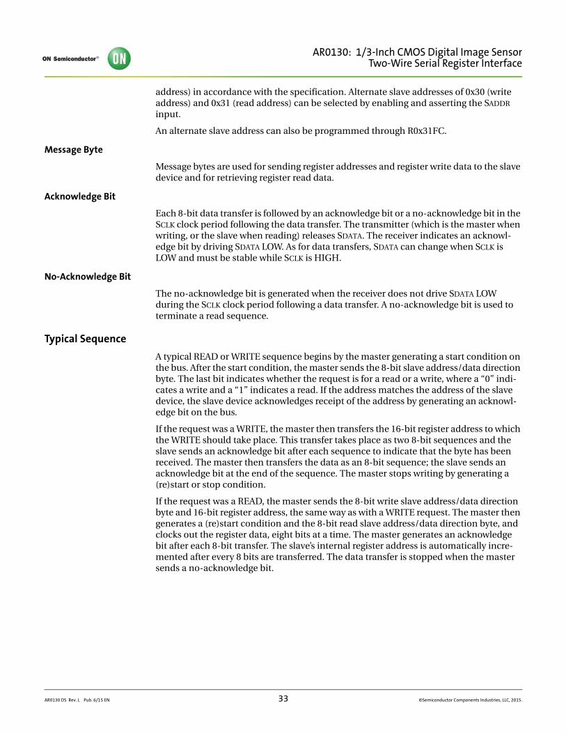
Single READ from Random Location
This sequence (Figure 20) starts with a dummy WRITE to the 16-bit address that is to be used for the READ. The master terminates the WRITE by generating a restart condition. The master then sends the 8-bit read slave address/data direction byte and clocks out one byte of register data. The master terminates the READ by generating a no-acknowl-edge bit followed by a stop condition. Figure 20 shows how the internal register address maintained by the AR0130 is loaded and incremented as the sequence proceeds.
Figure 20: Single READ from Random Location
Single READ from Current Location
This sequence (Figure 21) performs a read using the current value of the AR0130 internal register address. The master terminates the READ by generating a no-acknowledge bit followed by a stop condition. The figure shows two independent READ sequences.
Figure 21: Single READ from Current Location
Sequential READ, Start from Random Location
This sequence (Figure 22) starts in the same way as the single READ from random loca-tion (Figure 20). Instead of generating a no-acknowledge bit after the first byte of data has been transferred, the master generates an acknowledge bit and continues to perform byte READs until “L” bytes have been read.
Figure 22: Sequential READ, Start from Random Location
S = start conditionP = stop conditionSr = restart conditionA = acknowledgeA = no-acknowledge
slave to mastermaster to slave
Slave Address 0S A Reg Address[15:8] A Reg Address[7:0] Slave Address AA 1Sr Read Data P
Previous Reg Address, N Reg Address, M M+1
A
Slave Address 1S A Read Data Slave Address A1SP Read Data P
Previous Reg Address, N Reg Address, N+1 N+2
AA
Slave Address 0S SrA Reg Address[15:8]
Read Data Read Data
A Reg Address[7:0] A Read DataSlave Address
Previous Reg Address, N Reg Address, M
M+1 M+2
M+1
M+3
A1
Read Data Read Data
M+L-2 M+L-1 M+L
A P
A
AAA
AR0130 DS Rev. L Pub. 6/15 EN 34 ©Semiconductor Components Industries, LLC, 2015.
AR0130: 1/3-Inch CMOS Digital Image SensorTwo-Wire Serial Register Interface
Sequential READ, Start from Current Location
This sequence (Figure 23) starts in the same way as the single READ from current loca-tion (Figure 21). Instead of generating a no-acknowledge bit after the first byte of data has been transferred, the master generates an acknowledge bit and continues to perform byte READs until “L” bytes have been read.
Figure 23: Sequential READ, Start from Current Location
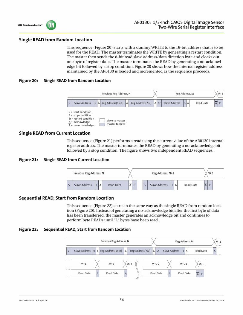
Single WRITE to Random Location
This sequence (Figure 24) begins with the master generating a start condition. The slave address/data direction byte signals a WRITE and is followed by the HIGH then LOW bytes of the register address that is to be written. The master follows this with the byte of write data. The WRITE is terminated by the master generating a stop condition.
Figure 24: Single WRITE to Random Location
Sequential WRITE, Start at Random Location
This sequence (Figure 25) starts in the same way as the single WRITE to random location (Figure 24). Instead of generating a no-acknowledge bit after the first byte of data has been transferred, the master generates an acknowledge bit and continues to perform byte WRITEs until “L” bytes have been written. The WRITE is terminated by the master generating a stop condition.
Figure 25: Sequential WRITE, Start at Random Location
Read Data Read Data
Previous Reg Address, N N+1 N+2 N+L-1 N+L
Read DataSlave Address A1 Read Data A PS A A A
Slave Address 0S A Reg Address[15:8] A Reg Address[7:0] A P
Previous Reg Address, N Reg Address, M M+1
AA
Write Data
Slave Address 0S A Reg Address[15:8]
A
A Reg Address[7:0] A
Previous Reg Address, N Reg Address, M
M+1 M+2
M+1
M+3
A
A A
M+L-2 M+L-1 M+L
AA P
Write Data
Write Data Write Data Write DataWrite Data
AR0130 DS Rev. L Pub. 6/15 EN 35 ©Semiconductor Components Industries, LLC, 2015.
AR0130: 1/3-Inch CMOS Digital Image SensorSpectral Characteristics
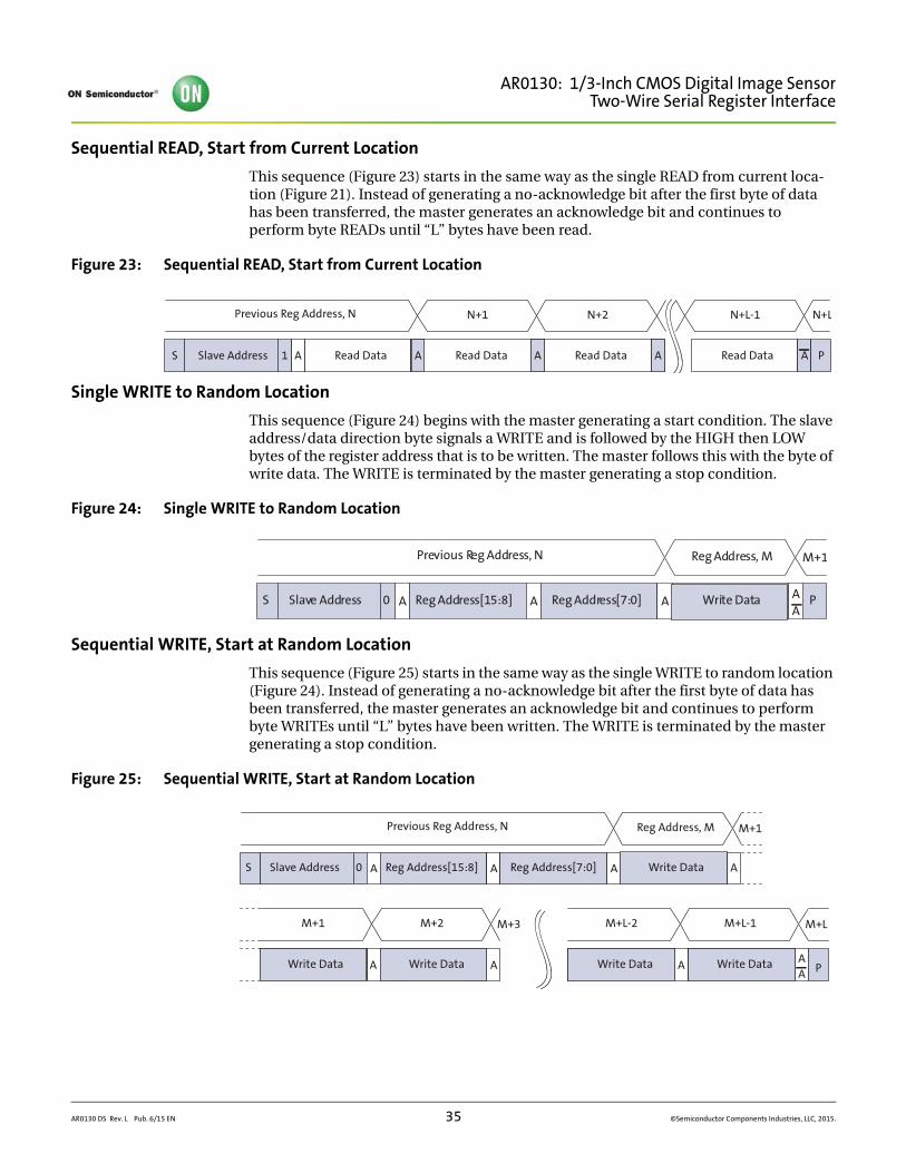
Spectral Characteristics
Figure 26: Quantum Efficiency – Monochrome Sensor
0
10
20
30
40
50
60
70
80
90
350 450 550 650 750 850 950 1050 1150
Qu
antu
m E
ffic
ien
cy (
%)
Wavelength (nm)
AR0130 DS Rev. L Pub. 6/15 EN 36 ©Semiconductor Components Industries, LLC, 2015.
AR0130: 1/3-Inch CMOS Digital Image SensorSpectral Characteristics
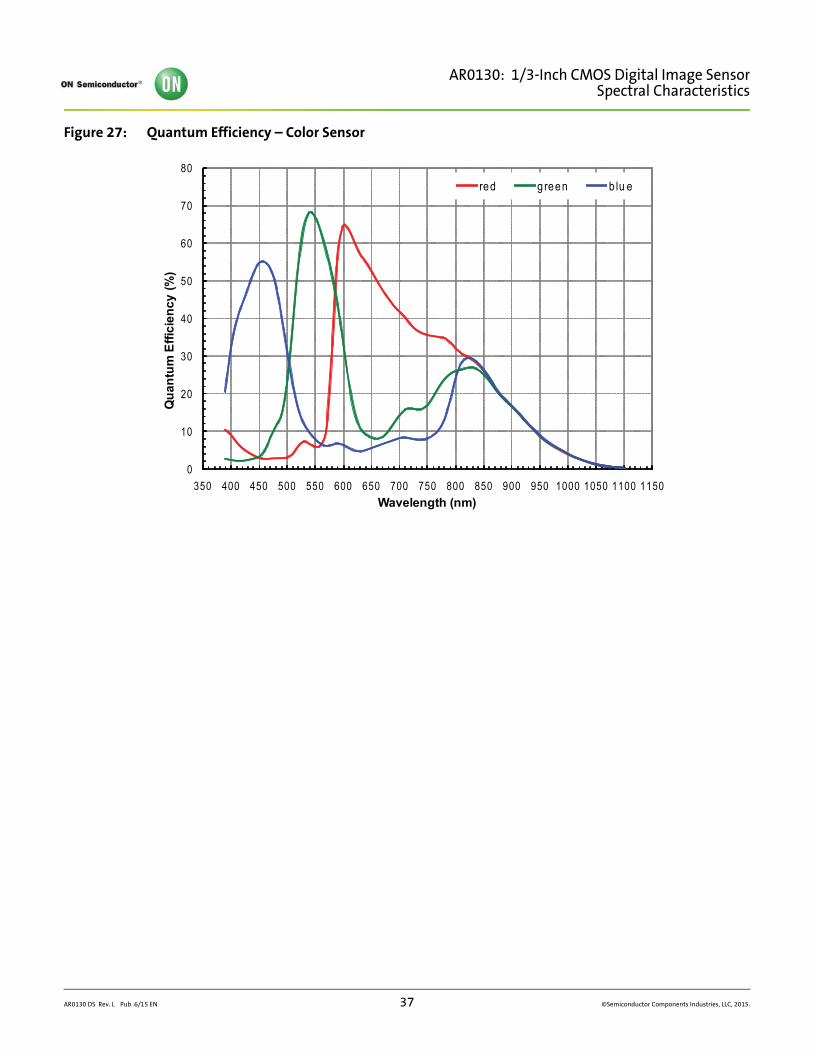
Figure 27: Quantum Efficiency – Color Sensor
0
10
20
30
40
50
60
70
80
350 400 450 500 550 600 650 700 750 800 850 900 950 1000 1050 1100 1150
Qua
ntum
Effi
cien
cy (%
)
Wavelength (nm)
red g reen b lu e
AR0130 DS Rev. L Pub. 6/15 EN 37 ©Semiconductor Components Industries, LLC, 2015.
AR0130 D
S Rev. L Pub. 6/15 EN
38©
Semicon
ductor C
ompon
ents In
dustries, LLC
, 2015
AR0130: 1/3-Inch CM
OS D
igital Image Sensor
Package Dim
ensionsPackage Dimensions
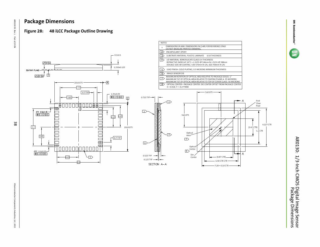
Figure 28: 48 iLCC Package Outline Drawing
First Clear Pixel
(3.67 CTR)
5.2 CTR
6.227 CTR
E CENTER:
ONSICRONS
0.2±0.1
1.250±0.125
1.35±0.05
0.725 TYP
4.454.15
0.525 TYP
0.125 TYP8.9
4.45DieCenter
OpticalCenter
OpticalArea
(4.87 CTR)
6.40 CTR CTR
7.28 = 0.10 CTR
8
7
2
4
3
6
10±0.075
5±0.075
5±0.075
0.4±0.0548X
5
3.85
7.7
0.15
0.15 A
A B
B
C
C
3.85
7.7
0.15 A B C
10±0.075
A
0.7 TYP
0.7 TYP
ENCAPSULANT: EPOXY
SUBSTRATE MATERIAL: PLASTIC LAMINATE 0.50 THICKNESS
LID MATERIAL: BOROSILICATE GLASS 0.4 THICKNESSREFRACTIVE INDEX AT 20°C = 1.5255 @ 546nm & 1.5231 @ 588nmDOUBLE SIDE AR COATING: 530-570nm R<1%; 420-700nm R<2%
LEAD FINISH: GOLD PLATING, 0.5 MICRONS MINIMUM THICKNESS
IMAGE SENSOR DIE
DIMENSIONS IN MM. DIMENSIONS IN () ARE FOR REFERENCE ONLY.DO NOT MEASURE PRINTED DRAWING.
NOTES
OPTICAL CENTER = PACKAGE CENTER. DIE CENTER OFFSET FROM PACKAGX = 0.018, Y = -0.277MM
MAXIMUM ROTATION OF OPTICAL AREA RELATIVE TO PACKAGE EDGES: 1°MAXIMUM TILT OF OPTICAL AREA RELATIVE TO SEATING PLANE A: 35 MICRMAXIMUM TILT OF OPTICAL AREA RELATIVE TO TOP OF COVER GLASS: 50 M
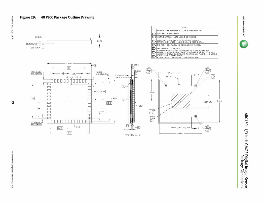
AR0130 D
S Rev. L Pub. 6/15 EN
39©
Semicon
ductor C
ompon
ents In
dustries, LLC
, 2015
AR0130: 1/3-Inch CM
OS D
igital Image Sensor
Package Dim
ensionsFigure 29: 48 PLCC Package Outline Drawing
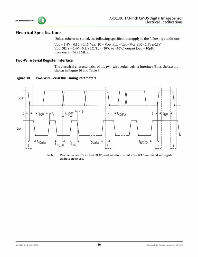
AR0130: 1/3-Inch CMOS Digital Image SensorElectrical Specifications
Electrical SpecificationsUnless otherwise stated, the following specifications apply to the following conditions:
VDD = 1.8V – 0.10/+0.15; VDD_IO = VDD_PLL = VAA = VAA_PIX = 2.8V ± 0.3V; VDD_SLVS = 0.4V – 0.1/+0.2; TA = -30°C to +70°C; output load = 10pF; frequency = 74.25 MHz.
Two-Wire Serial Register Interface
The electrical characteristics of the two-wire serial register interface (SCLK, SDATA) are shown in Figure 30 and Table 8.
Figure 30: Two-Wire Serial Bus Timing Parameters
Note: Read sequence: For an 8-bit READ, read waveforms start after READ command and register address are issued.
S SrtSU;STOtSU;STAtHD;STA tHIGH
tLOW tSU;DAT
tHD;DAT
tf
SDATA
SCLK
P S
tBUFtrtftr tHD;STA
AR0130 DS Rev. L Pub. 6/15 EN 40 ©Semiconductor Components Industries, LLC, 2015.
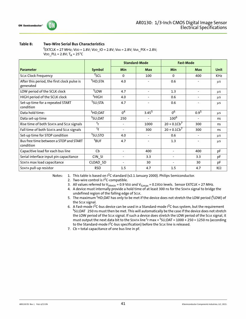
AR0130: 1/3-Inch CMOS Digital Image SensorElectrical Specifications
Notes: 1. This table is based on I2C standard (v2.1 January 2000). Philips Semiconductor.2. Two-wire control is I2C-compatible. 3. All values referred to VIHmin = 0.9 VDD and VILmax = 0.1VDD levels. Sensor EXTCLK = 27 MHz. 4. A device must internally provide a hold time of at least 300 ns for the SDATA signal to bridge the
undefined region of the falling edge of SCLK. 5. The maximum tHD;DAT has only to be met if the device does not stretch the LOW period (tLOW) of
the SCLK signal.6. A Fast-mode I2C-bus device can be used in a Standard-mode I2C-bus system, but the requirement
tSU;DAT 250 ns must then be met. This will automatically be the case if the device does not stretch the LOW period of the SCLK signal. If such a device does stretch the LOW period of the SCLK signal, it must output the next data bit to the SDATA line tr max + tSU;DAT = 1000 + 250 = 1250 ns (according to the Standard-mode I2C-bus specification) before the SCLK line is released.
7. Cb = total capacitance of one bus line in pF.
Table 8: Two-Wire Serial Bus CharacteristicsfEXTCLK = 27 MHz; VDD = 1.8V; VDD_IO = 2.8V; VAA = 2.8V; VAA_PIX = 2.8V;VDD_PLL = 2.8V; TA = 25°C
Parameter Symbol
Standard-Mode Fast-Mode
UnitMin Max Min Max
SCLK Clock Frequency fSCL 0 100 0 400 KHz
After this period, the first clock pulse is generated
tHD;STA 4.0 - 0.6 - s
LOW period of the SCLK clock tLOW 4.7 - 1.3 - s
HIGH period of the SCLK clock tHIGH 4.0 - 0.6 - s
Set-up time for a repeated START condition
tSU;STA 4.7 - 0.6 - s
Data hold time: tHD;DAT 04 3.455 06 0.95 s
Data set-up time tSU;DAT 250 - 1006 - ns
Rise time of both SDATA and SCLK signals tr - 1000 20 + 0.1Cb7 300 ns
Fall time of both SDATA and SCLK signals tf - 300 20 + 0.1Cb7 300 ns
Set-up time for STOP condition tSU;STO 4.0 - 0.6 - s
Bus free time between a STOP and START condition
tBUF 4.7 - 1.3 - s
Capacitive load for each bus line Cb - 400 - 400 pF
Serial interface input pin capacitance CIN_SI - 3.3 - 3.3 pF
SDATA max load capacitance CLOAD_SD - 30 - 30 pF
SDATA pull-up resistor RSD 1.5 4.7 1.5 4.7 K
AR0130 DS Rev. L Pub. 6/15 EN 41 ©Semiconductor Components Industries, LLC, 2015.
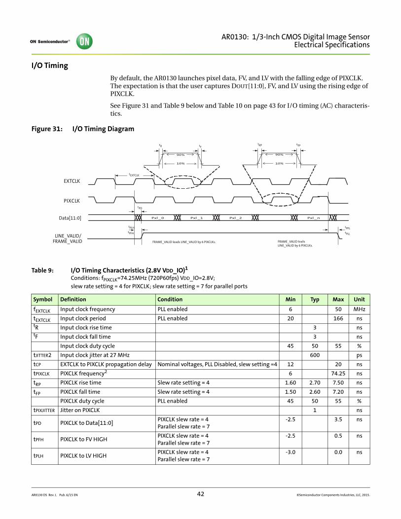
AR0130: 1/3-Inch CMOS Digital Image SensorElectrical Specifications
I/O Timing
By default, the AR0130 launches pixel data, FV, and LV with the falling edge of PIXCLK. The expectation is that the user captures DOUT[11:0], FV, and LV using the rising edge of PIXCLK.
See Figure 31 and Table 9 below and Table 10 on page 43 for I/O timing (AC) characteris-tics.
Figure 31: I/O Timing Diagram
Table 9: I/O Timing Characteristics (2.8V VDD_IO)1
Conditions: fPIXCLK=74.25MHz (720P60fps) VDD_IO=2.8V; slew rate setting = 4 for PIXCLK; slew rate setting = 7 for parallel ports
Symbol Definition Condition Min Typ Max Unit
fEXTCLK Input clock frequency PLL enabled 6 50 MHz
tEXTCLK Input clock period PLL enabled 20 166 nstR Input clock rise time 3 nstF Input clock fall time 3 ns
Input clock duty cycle 45 50 55 %
tJITTER2 Input clock jitter at 27 MHz 600 ps
tCP EXTCLK to PIXCLK propagation delay Nominal voltages, PLL Disabled, slew setting =4 12 20 ns
tPIXCLK PIXCLK frequency2 6 74.25 ns
tRP PIXCLK rise time Slew rate setting = 4 1.60 2.70 7.50 ns
tFP PIXCLK fall time Slew rate setting = 4 1.50 2.60 7.20 ns
PIXCLK duty cycle PLL enabled 45 50 55 %
tPIXJITTER Jitter on PIXCLK 1 ns
tPD PIXCLK to Data[11:0]PIXCLK slew rate = 4Parallel slew rate = 7
-2.5 3.5 ns
tPFH PIXCLK to FV HIGHPIXCLK slew rate = 4Parallel slew rate = 7
-2.5 0.5 ns
tPLH PIXCLK to LV HIGHPIXCLK slew rate = 4Parallel slew rate = 7
-3.0 0.0 ns
Data[11:0]
LINE_VALID/
PIXCLK
EXTCLK
tR
tEXTCLK
tF
FRAME_VALID leads LINE_VALID by 6 PIXCLKs.
FRAME_VALID trailsLINE_VALID by 6 PIXCLKs.
tPLH
tPFH
tPFL
tPLL
tPD
Pxl _0 Pxl _1 Pxl _2 Pxl _n
90%
10%
tRP tFP
90%
10%
FRAME_VALID
AR0130 DS Rev. L Pub. 6/15 EN 42 ©Semiconductor Components Industries, LLC, 2015.
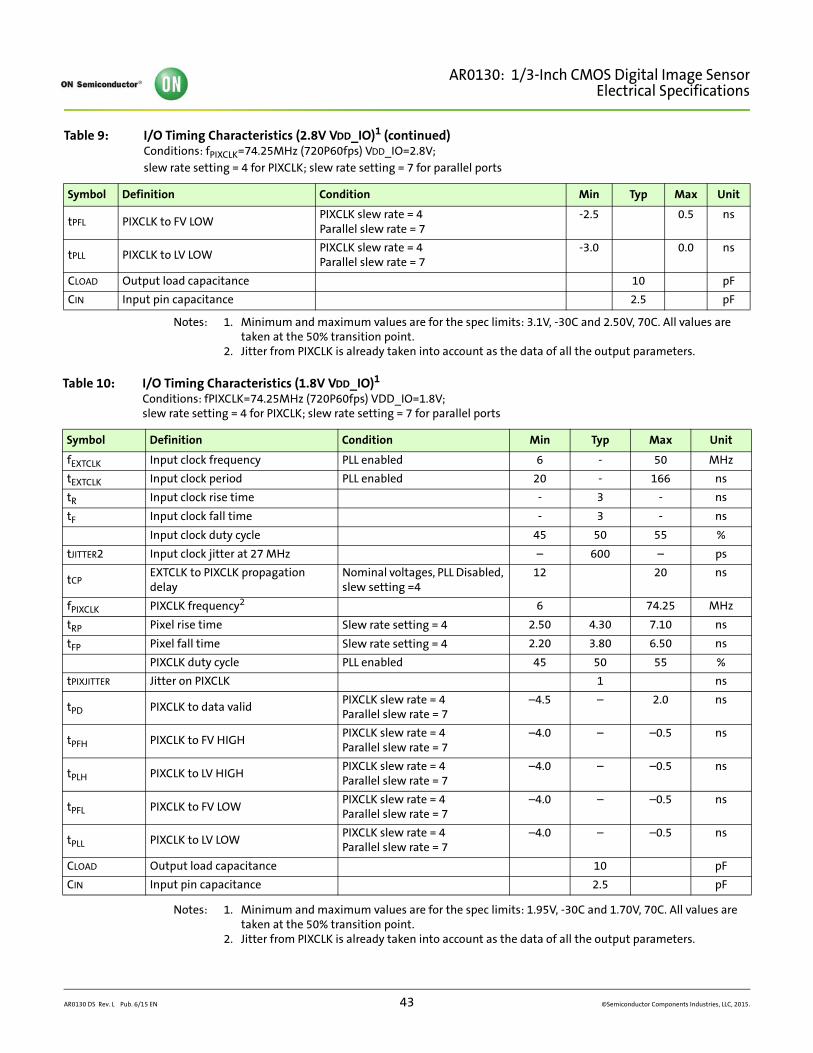
AR0130: 1/3-Inch CMOS Digital Image SensorElectrical Specifications
Notes: 1. Minimum and maximum values are for the spec limits: 3.1V, -30C and 2.50V, 70C. All values are taken at the 50% transition point.
2. Jitter from PIXCLK is already taken into account as the data of all the output parameters.
Notes: 1. Minimum and maximum values are for the spec limits: 1.95V, -30C and 1.70V, 70C. All values are taken at the 50% transition point.
2. Jitter from PIXCLK is already taken into account as the data of all the output parameters.
tPFL PIXCLK to FV LOWPIXCLK slew rate = 4Parallel slew rate = 7
-2.5 0.5 ns
tPLL PIXCLK to LV LOWPIXCLK slew rate = 4Parallel slew rate = 7
-3.0 0.0 ns
CLOAD Output load capacitance 10 pF
CIN Input pin capacitance 2.5 pF
Table 10: I/O Timing Characteristics (1.8V VDD_IO)1
Conditions: fPIXCLK=74.25MHz (720P60fps) VDD_IO=1.8V;slew rate setting = 4 for PIXCLK; slew rate setting = 7 for parallel ports
Symbol Definition Condition Min Typ Max Unit
fEXTCLK Input clock frequency PLL enabled 6 - 50 MHz
tEXTCLK Input clock period PLL enabled 20 - 166 ns
tR Input clock rise time - 3 - ns
tF Input clock fall time - 3 - ns
Input clock duty cycle 45 50 55 %
tJITTER2 Input clock jitter at 27 MHz – 600 – ps
tCPEXTCLK to PIXCLK propagation delay
Nominal voltages, PLL Disabled, slew setting =4
12 20 ns
fPIXCLK PIXCLK frequency2 6 74.25 MHz
tRP Pixel rise time Slew rate setting = 4 2.50 4.30 7.10 ns
tFP Pixel fall time Slew rate setting = 4 2.20 3.80 6.50 ns
PIXCLK duty cycle PLL enabled 45 50 55 %
tPIXJITTER Jitter on PIXCLK 1 ns
tPD PIXCLK to data validPIXCLK slew rate = 4Parallel slew rate = 7
–4.5 – 2.0 ns
tPFH PIXCLK to FV HIGHPIXCLK slew rate = 4Parallel slew rate = 7
–4.0 – –0.5 ns
tPLH PIXCLK to LV HIGHPIXCLK slew rate = 4Parallel slew rate = 7
–4.0 – –0.5 ns
tPFL PIXCLK to FV LOWPIXCLK slew rate = 4Parallel slew rate = 7
–4.0 – –0.5 ns
tPLL PIXCLK to LV LOWPIXCLK slew rate = 4Parallel slew rate = 7
–4.0 – –0.5 ns
CLOAD Output load capacitance 10 pF
CIN Input pin capacitance 2.5 pF
Table 9: I/O Timing Characteristics (2.8V VDD_IO)1 (continued)Conditions: fPIXCLK=74.25MHz (720P60fps) VDD_IO=2.8V; slew rate setting = 4 for PIXCLK; slew rate setting = 7 for parallel ports
Symbol Definition Condition Min Typ Max Unit
AR0130 DS Rev. L Pub. 6/15 EN 43 ©Semiconductor Components Industries, LLC, 2015.
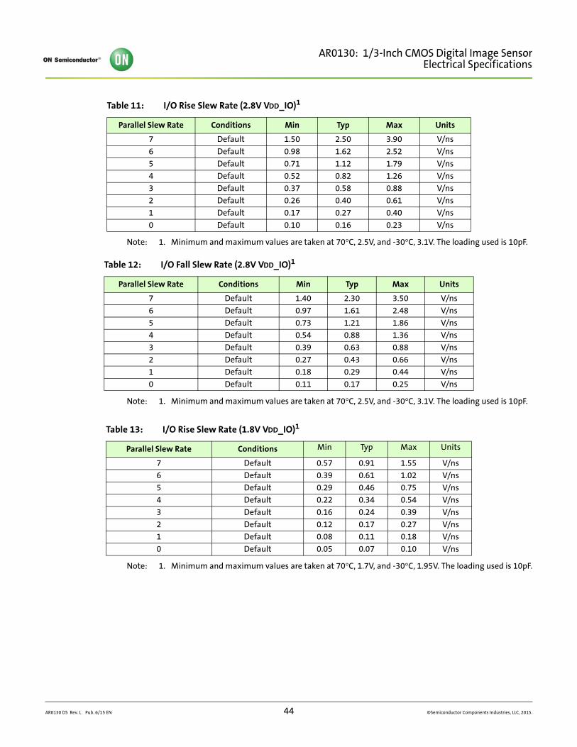
AR0130: 1/3-Inch CMOS Digital Image SensorElectrical Specifications
Note: 1. Minimum and maximum values are taken at 70°C, 2.5V, and -30°C, 3.1V. The loading used is 10pF.
Note: 1. Minimum and maximum values are taken at 70°C, 2.5V, and -30°C, 3.1V. The loading used is 10pF.
Note: 1. Minimum and maximum values are taken at 70°C, 1.7V, and -30°C, 1.95V. The loading used is 10pF.
Table 11: I/O Rise Slew Rate (2.8V VDD_IO)1
Parallel Slew Rate Conditions Min Typ Max Units
7 Default 1.50 2.50 3.90 V/ns
6 Default 0.98 1.62 2.52 V/ns
5 Default 0.71 1.12 1.79 V/ns
4 Default 0.52 0.82 1.26 V/ns
3 Default 0.37 0.58 0.88 V/ns
2 Default 0.26 0.40 0.61 V/ns
1 Default 0.17 0.27 0.40 V/ns
0 Default 0.10 0.16 0.23 V/ns
Table 12: I/O Fall Slew Rate (2.8V VDD_IO)1
Parallel Slew Rate Conditions Min Typ Max Units
7 Default 1.40 2.30 3.50 V/ns
6 Default 0.97 1.61 2.48 V/ns
5 Default 0.73 1.21 1.86 V/ns
4 Default 0.54 0.88 1.36 V/ns
3 Default 0.39 0.63 0.88 V/ns
2 Default 0.27 0.43 0.66 V/ns
1 Default 0.18 0.29 0.44 V/ns
0 Default 0.11 0.17 0.25 V/ns
Table 13: I/O Rise Slew Rate (1.8V VDD_IO)1
Parallel Slew Rate Conditions Min Typ Max Units
7 Default 0.57 0.91 1.55 V/ns
6 Default 0.39 0.61 1.02 V/ns
5 Default 0.29 0.46 0.75 V/ns
4 Default 0.22 0.34 0.54 V/ns
3 Default 0.16 0.24 0.39 V/ns
2 Default 0.12 0.17 0.27 V/ns
1 Default 0.08 0.11 0.18 V/ns
0 Default 0.05 0.07 0.10 V/ns
AR0130 DS Rev. L Pub. 6/15 EN 44 ©Semiconductor Components Industries, LLC, 2015.
AR0130: 1/3-Inch CMOS Digital Image SensorElectrical Specifications
Note: 1. Minimum and maximum values are taken at 70°C, 1.7V, and -30°C, 1.95V. The loading used is 10pF.
DC Electrical Characteristics
The DC electrical characteristics are shown in the tables below.
Table 15: DC Electrical Characteristics
Table 14: I/O Fall Slew Rate (1.8V VDD_IO)1
Parallel Slew Rate Conditions Min Typ Max Units
7 Default 0.57 0.92 1.55 V/ns
6 Default 0.40 0.64 1.08 V/ns
5 Default 0.31 0.50 0.82 V/ns
4 Default 0.24 0.38 0.61 V/ns
3 Default 0.18 0.27 0.44 V/ns
2 Default 0.13 0.19 0.31 V/ns
1 Default 0.09 0.13 0.20 V/ns
0 Default 0.05 0.08 0.12 V/ns
Symbol Definition Condition Min Typ Max Unit
VDD Core digital voltage 1.7 1.8 1.95 V
VDD_IO I/O digital voltage 1.7/2.5 1.8/2.8 1.9/3.1 V
VAA Analog voltage 2.5 2.8 3.1 V
VAA_PIX Pixel supply voltage 2.5 2.8 3.1 V
VDD_PLL PLL supply voltage 2.5 2.8 3.1 V
VDD_SLVS Digital supply voltage Do not connect. – – – V
VIH Input HIGH voltage VDD_IO*0.7 – – V
VIL Input LOW voltage – – VDD_IO*0.3 V
IIN Input leakage currentNo pull-up resistor; VIN = VDD_IO or DGND
20 – – A
VOH Output HIGH voltage VDD_IO-0.3 – – V
VOL Output LOW voltage – – 0.4 V
IOH Output HIGH current At specified VOH -22 – – mA
IOL Output LOW current At specified VOL – – 22 mA
AR0130 DS Rev. L Pub. 6/15 EN 45 ©Semiconductor Components Industries, LLC, 2015.
AR0130: 1/3-Inch CMOS Digital Image SensorElectrical Specifications
Caution Stresses greater than those listed in Table 16 may cause permanent damage to the device. This is a stress rating only, and functional operation of the device at these or any other con-ditions above those indicated in the operational sections of this specification is not implied.
Notes: 1. Exposure to absolute maximum rating conditions for extended periods may affect reliability.2. To keep dark current and shot noise artifacts from impacting image quality, keep operating tem-
perature at a minimum.
Notes: 1. Operating currents are measured at the following conditions:VAA=VAA_PIX=VDD_IO=VDD_PLL=2.8VVDD=1.8VPLL Enabled and PIXCLK=74.25MHzTA = 25°C
Table 16: Absolute Maximum Ratings
Symbol Parameter Minimum Maximum Unit
VSUPPLYPower supply voltage (VDD and VAA supplies)
–0.3 4.5 V
ISUPPLY Total power supply current – 200 mA
IGND Total ground current – 200 mA
VIN DC input voltage –0.3 VDD_IO + 0.3 V
VOUT DC output voltage –0.3 VDD_IO + 0.3 V
TSTG1 Storage temperature –40 +85 °C
Table 17: Operating Current Consumption in Parallel Output
Definition Condition Symbol Min Typ Max Unit
Digital operating current Streaming, 1280x960 45fps IDD1 – 40 65 mA
I/O digital operating current Streaming, 1280x960 45fpsIDD_IO – 35 – mA
Analog operating current Streaming, 1280x960 45fps IAA – 30 55 mA
Pixel supply current Streaming, 1280x960 45fps IAA_PIX – 10 15 mA
PLL supply current Streaming, 1280x960 45fps IDD_PLL – 7 – mA
Digital operating current Streaming, 720p 60fps IDD1 – 40 – mA
I/O digital operating current Streaming, 720p 60fpsIDD_IO - 35 – mA
Analog operating current Streaming, 720p 60fps IAA – 30 – mA
Pixel supply current Streaming, 720p 60fps IAA_PIX – 10 15 mA
PLL supply current Streaming, 720p 60fps IDD_PLL – 7 – mA
AR0130 DS Rev. L Pub. 6/15 EN 46 ©Semiconductor Components Industries, LLC, 2015.
AR0130: 1/3-Inch CMOS Digital Image SensorElectrical Specifications
Notes: 1. Analog – VAA + VAA_PIX + VDD_PLL2. Digital – VDD + VDD_IO + VDD_SLVS
Figure 32: Power Supply Rejection Ratio
Table 18: Standby Current Consumption
Definition Condition Symbol Min Typ Max Unit
Hard standby (clock off) Analog, 2.8V - – 70 200 μA
Digital, 1.8V - – 640 900 μA
Hard standby (clock on) Analog, 2.8V - – 275 – μA
Digital, 1.8V - – 1.55 – mA
Soft standby (clock off) Analog, 2.8V - – 70 200 μA
Digital, 1.8V - – 640 900 μA
Soft standby (clock on) Analog, 2.8V - – 275 – μA
Digital, 1.8V - – 1.55 – mA
0
10
20
30
40
50
60
70
1000 10000 100000 1000000
PSRR (dB)
Frequency (Hz)
Power Supply Rejection Ratio
AR0130 DS Rev. L Pub. 6/15 EN 47 ©Semiconductor Components Industries, LLC, 2015.
AR0130: 1/3-Inch CMOS Digital Image SensorPower-On Reset and Standby Timing
Power-On Reset and Standby Timing
Power-Up Sequence
The recommended power-up sequence for the AR0130 is shown in Figure 33. The avail-able power supplies (VDD_IO, VDD, VDD_SLVS, VDD_PLL, VAA, VAA_PIX) must have the separation specified below.1. Turn on VDD_PLL power supply.2. After 0–10s, turn on VAA and VAA_PIX power supply.3. After 0–10s, turn on VDD power supply.4. After 0–10s, turn on VDD_IO power supply.5. After the last power supply is stable, enable EXTCLK.6. Assert RESET_BAR for at least 1ms.7. Wait 150000 EXTCLKs (for internal initialization into software standby.8. Configure PLL, output, and image settings to desired values.9. Wait 1ms for the PLL to lock.
10. Set streaming mode (R0x301a[2] = 1).
Figure 33: Power Up
VDD_PLL (2.8)
VAA_PIXVAA (2.8)
VDD_IO (1.8/2.8)
VDD (1.8)
VDD_SLVS
EXTCLK
RESET_BAR
t0
t1
t2
t3
tx
t4
t5 t6
Hard ResetInternalInitialization
SoftwareStandby
PLL Lock Streaming
AR0130 DS Rev. L Pub. 6/15 EN 48 ©Semiconductor Components Industries, LLC, 2015.
AR0130: 1/3-Inch CMOS Digital Image SensorPower-On Reset and Standby Timing
Notes: 1. Xtal settling time is component-dependent, usually taking about 10 – 100 mS.2. Hard reset time is the minimum time required after power rails are settled. In a circuit where Hard
reset is held down by RC circuit, then the RC time must include the all power rail settle time and Xtal settle time.
3. It is critical that VDD_PLL is not powered up after the other power supplies. It must be powered before or at least at the same time as the others. If the case happens that VDD_PLL is powered after other supplies then sensor may have functionality issues and will experience high current draw on this supply.
4. For the case where VDD_IO is 2.8V and VDD is 1.8V, it is recommended that the minimum time be 5s.
Table 19: Power-Up Sequence
Definition Symbol Minimum Typical Maximum Unit
VDD_PLL to VAA/VAA_PIX3 t0 0 10 – s
VAA/VAA_PIX to VDD t1 0 10 – s
VDD to VDD_IO t2 04 10 – s
VDD_IO to VDD_SLVS t3 0 10 – s
Xtal settle time tx – 301 – ms
Hard Reset t4 12 – – ms
Internal Initialization t5 150000 – – EXTCLKs
PLL Lock Time t6 1 – – ms
AR0130 DS Rev. L Pub. 6/15 EN 49 ©Semiconductor Components Industries, LLC, 2015.
AR0130: 1/3-Inch CMOS Digital Image SensorPower-On Reset and Standby Timing
Power-Down Sequence
The recommended power-down sequence for the AR0130 is shown in Figure 34. The available power supplies (VDD_IO, VDD, VDD_SLVS, VDD_PLL, VAA, VAA_PIX) must have the separation specified below.1. Disable streaming if output is active by setting standby R0x301a[2] = 02. The soft standby state is reached after the current row or frame, depending on config-
uration, has ended.3. Turn off VDD_SLVS, if used.4. Turn off VDD_IO.5. Turn off VDD.6. Turn off VAA/VAA_PIX.7. Turn off VDD_PLL.
Figure 34: Power Down
Note: t4 is required between power down and next power up time; all decoupling caps from regulators must be completely discharged.
Table 20: Power-Down Sequence
Definition Symbol Minimum Typical Maximum Unit
VDD_SLVS to VDD_IO t0 0 – – s
VDD_IO to VDD t1 0 – – s
VDD to VAA/VAA_PIX t2 0 – – s
VAA/VAA_PIX to VDD_PLL t3 0 – – s
PwrDn until Next PwrUp Time t4 100 – – ms
V DD_IO (1.8/2.8)
t4
t 0
t1
t3
t2
EXTCLK
VDD_SLVS
VDD (1.8)
VAA_PIXVAA (2.8)
VDD_PLL (2.8)
Power Down until next Power up cycle
AR0130 DS Rev. L Pub. 6/15 EN 50 ©Semiconductor Components Industries, LLC, 2015.
AR0130: 1/3-Inch CMOS Digital Image SensorRevision History
Revision HistoryRev. L . . . . . . . . . . . . . . . . . . . . . . . . . . . . . . . . . . . . . . . . . . . . . . . . . . . . . . . . . . . . . . . . . . . . . . . . . . . . . . . . . . . . . . . . . . . . . 6/9/15
• Updated “Ordering Information” on page 2
Rev. K . . . . . . . . . . . . . . . . . . . . . . . . . . . . . . . . . . . . . . . . . . . . . . . . . . . . . . . . . . . . . . . . . . . . . . . . . . . . . . . . . . . . . . . . . . . .4/13/15• Updated “Ordering Information” on page 2
Rev. J. . . . . . . . . . . . . . . . . . . . . . . . . . . . . . . . . . . . . . . . . . . . . . . . . . . . . . . . . . . . . . . . . . . . . . . . . . . . . . . . . . . . . . . . . . . . .3/25/15• Removed Confidential marking• Updated Table of Contents format
Rev. H . . . . . . . . . . . . . . . . . . . . . . . . . . . . . . . . . . . . . . . . . . . . . . . . . . . . . . . . . . . . . . . . . . . . . . . . . . . . . . . . . . . . . . . . . . .11/11/14• Updated to ON Semiconductor template
Rev. G . . . . . . . . . . . . . . . . . . . . . . . . . . . . . . . . . . . . . . . . . . . . . . . . . . . . . . . . . . . . . . . . . . . . . . . . . . . . . . . . . . . . . . . . . . . .2/25/14• Updated Table 1, “Key Parameters,” on page 1• Updated Table 3, “,” on page 2• Updated Figure 6, Pixel Color Pattern Detail (Top Right Corner)• Updated “Default Readout Order” on page 12• Updated note to Table 5, “Frame Time: Long Integration Time,” on page 16• Updated Equation 2 on page 16• Updated “Hard Standby” on page 21• Updated “I/O Timing” on page 42• Replaced Table 9, “I/O Timing Characteristics with Table 9, “I/O Timing Characteris-
tics (2.8V Vdd_IO)1,” on page 42 and Table 10, “I/O Timing Characteristics (1.8V Vdd_IO)1,” on page 43
• Added Table 11, “I/O Rise Slew Rate (2.8V Vdd_IO)1,” on page 44• Added Table 12, “I/O Fall Slew Rate (2.8V Vdd_IO)1,” on page 44• Added Table 13, “I/O Rise Slew Rate (1.8V Vdd_IO)1,” on page 44• Added Table 14, “I/O Fall Slew Rate (1.8V Vdd_IO)1,” on page 45• Added Figure 32: “Power Supply Rejection Ratio,” on page 47
Rev. F . . . . . . . . . . . . . . . . . . . . . . . . . . . . . . . . . . . . . . . . . . . . . . . . . . . . . . . . . . . . . . . . . . . . . . . . . . . . . . . . . . . . . . . . . . . .3/14/13• Updated Table 1, “Key Parameters,” on page 1• Updated Table 2, “Available Part Numbers,” on page 1• Updated Note 1 in “General Description” on page 6• Updated “PLL-Generated Master Clock” on page 18• Added Figure 13, Enter Standby Timing and Figure 14: “Exit Standby Timing,” on
page 20• Updated “Bayer Space Resampling” on page 22• Updated Figure 15: “Six Pixels in Normal and Column Mirror Readout Modes,” on
page 22• Updated Figure 16: “Six Rows in Normal and Row Mirror Readout Modes,” on page 23• Updated “Image Acquisition Modes” on page 25• Updated “Automatic Exposure Control” on page 26• Updated “Embedded Data and Statistics” on page 26• Updated “Analog Gain” on page 29• Updated “Black Level Correction” on page 29• Updated “Column Triggering on Startup” on page 30
AR0130 DS Rev. L Pub. 6/15 EN 51 ©Semiconductor Components Industries, LLC, 2015.
AR0130: 1/3-Inch CMOS Digital Image SensorRevision History
• Updated “Column Correction Retriggering Due to Mode Change” on page 30• Updated Figure 26: “Quantum Efficiency – Monochrome Sensor,” on page 36• Updated Note 4 in Figure 28: “48 iLCC Package Outline Drawing,” on page 38
Rev. E . . . . . . . . . . . . . . . . . . . . . . . . . . . . . . . . . . . . . . . . . . . . . . . . . . . . . . . . . . . . . . . . . . . . . . . . . . . . . . . . . . . . . . . . . . . . . 6/5/12• Updated Table 2, “Available Part Numbers,” on page 1• Updated “General Description” on page 6
Rev. D . . . . . . . . . . . . . . . . . . . . . . . . . . . . . . . . . . . . . . . . . . . . . . . . . . . . . . . . . . . . . . . . . . . . . . . . . . . . . . . . . . . . . . . . . . . .3/19/12• Updated to Production• Removed section “Defective Pixel Correction• Updated Table 9, “I/O Timing Characteristics,” on page 41• Updated Table 17, “Operating Current Consumption in Parallel Output ,” on page 46• Updated Table 18, “Standby Current Consumption ,” on page 47
Rev. C . . . . . . . . . . . . . . . . . . . . . . . . . . . . . . . . . . . . . . . . . . . . . . . . . . . . . . . . . . . . . . . . . . . . . . . . . . . . . . . . . . . . . . . . . . . .2/16/12• Updated “Features” on page 17• Updated Table 1, “Key Parameters,” on page 1• Updated Table 2, “Available Part Numbers,” on page 1• Updated “General Description” on page 6• Updated Figure 1: “Block Diagram,” on page 6• Deleted Figure 2: “Typical Configuration: Serial Four-Lane HiSPi Interface” from p.6
and renumbered remaining figures.• Updated notes for Figure 2: “Typical Configuration: Parallel Pixel Data Interface,” on
page 7• Updated Table 3, “Pad Descriptions,” on page 8• Updated Figure 3: “48-Pin iLCC Pinout Diagram,” on page 9• Added Figure 4: “48-Pin PLCC Pinout Diagram,” on page 10• Deleted section “Serial Output Data Timing”• Updated title of Figure 26: “Quantum Efficiency – Monochrome Sensor,” on page 36• Updated Figure 27: “Quantum Efficiency – Color Sensor,” on page 37• Added Figure 29: “48 PLCC Package Outline Drawing,” on page 39• Updated “Electrical Specifications” on page 40• Updated Table 8, “Two-Wire Serial Bus Characteristics,” on page 41• Updated Table 15, “DC Electrical Characteristics,” on page 45• Updated Table 16, “Absolute Maximum Ratings,” on page 46• Deleted Table 13: Operating Currents in HiSPi Output and renumbered succeeding
tables• Deleted section “HiSPi Electrical Specifications”• Updated Figure 33: “Power Up,” on page 48• Updated “Power-Down Sequence” on page 50• Updated Figure 34: “Power Down,” on page 50
Rev. B . . . . . . . . . . . . . . . . . . . . . . . . . . . . . . . . . . . . . . . . . . . . . . . . . . . . . . . . . . . . . . . . . . . . . . . . . . . . . . . . . . . . . . . . . . . .9/12/11• Updated “Features” on page 17• Updated Table 1, “Key Parameters,” on page 1• Updated Table 2, “Available Part Numbers,” on page 1• Added note to Figure 2: “Typical Configuration: Parallel Pixel Data Interface,” on
page 7
AR0130 DS Rev. L Pub. 6/15 EN 52 ©Semiconductor Components Industries, LLC, 2015.
AR0130: 1/3-Inch CMOS Digital Image SensorRevision History
• Updated note 4 in Figure 2: “Typical Configuration: Parallel Pixel Data Interface,” on page 7
• Added Figure 3: “48-Pin iLCC Pinout Diagram,” on page 9• Updated “Parallel Output Data Timing” on page 14• Updated Figure 12: “Timing Diagram,” on page 15• Updated Table 4, “Frame Time (Example Based on 1280 x 960, 45 Frames Per
Second),” on page 15• Updated Table 6, “Real-Time Context-Switchable Registers,” on page 17• Updated “To Configure and Use the PLL:” on page 18• Updated “To Enter Soft Standby:” on page 19• Updated “Single Frame” on page 25• Deleted “Temperature Sensor”• Updated “Embedded Statistics” on page 27• Updated “Column Correction Retriggering Due to Mode Change” on page 30• Added Figure 28: “48 iLCC Package Outline Drawing,” on page 38• Updated Figure 30: “Two-Wire Serial Bus Timing Parameters,” on page 40• Updated Table 8, “Two-Wire Serial Bus Characteristics,” on page 41• Updated note 1 in Table 18, “Standby Current Consumption ,” on page 47• Updated “Power-Up Sequence” on page 48• Updated Figure 33: “Power Up,” on page 48• Updated Table 19, “Power-Up Sequence,” on page 49• Updated “Power-Down Sequence” on page 50• Updated Figure 34: “Power Down,” on page 50• Updated Table 20, “Power-Down Sequence,” on page 50
Rev. A . . . . . . . . . . . . . . . . . . . . . . . . . . . . . . . . . . . . . . . . . . . . . . . . . . . . . . . . . . . . . . . . . . . . . . . . . . . . . . . . . . . . . . . . . . . . . 3/1/11• Initial release
ON Semiconductor and the ON logo are registered trademarks of Semiconductor Components Industries, LLC (SCILLC) or its subsidiaries in the United States and/or other countries. SCILLC owns therights to a number of patents, trademarks, copyrights, trade secrets, and other intellectual property. A listing of SCILLC’s product/patent coverage may be accessed at www.onsemi.com/site/pdf/Patent-Marking.pdf. SCILLC reserves the right to make changes without further notice to any products herein. SCILLC makes no warranty, representation or guarantee regarding the suitability of itsproducts for any particular purpose, nor does SCILLC assume any liability arising out of the application or use of any product or circuit, and specifically disclaims any and all liability, includingwithout limitation special, consequential or incidental damages. “Typical” parameters which may be provided in SCILLC data sheets and/or specifications can and do vary in different applicationsand actual performance may vary over time. All operating parameters, including “Typicals” must be validated for each customer application by customer’s technical experts. SCILLC does not conveyany license under its patent rights nor the rights of others. SCILLC products are not designed, intended, or authorized for use as components in systems intended for surgical implant into the body,or other applications intended to support or sustain life, or for any other application in which the failure of the SCILLC product could create a situation where personal injury or death may occur.Should Buyer purchase or use SCILLC products for any such unintended or unauthorized application, Buyer shall indemnify and hold SCILLC and its officers, employees, subsidiaries, affiliates, anddistributors harmless against all claims, costs, damages, and expenses, and reasonable attorney fees arising out of, directly or indirectly, any claim of personal injury or death associated with suchunintended or unauthorized use, even if such claim alleges that SCILLC was negligent regarding the design or manufacture of the part. SCILLC is an Equal Opportunity/Affirmative Action Employer.This literature is subject to all applicable copyright laws and is not for resale in any manner.
AR0130 DS Rev. L Pub. 6/15 EN 53 ©Semiconductor Components Industries, LLC, 2015 .


![PC1089K CDS V05 20101105 [호환 모드] - TradeKeyimgusr.tradekey.com/images/uploadedimages/brochures/5/1/6239624... · PC1089K 1/3 inch NTSC/PAL CMOS Image Sensor with PRELIMINARY](https://img.pdfslide.tips/doc/110x75/5aba9b967f8b9a567c8bb461/pc1089k-cds-v05-20101105-13-inch-ntscpal-cmos-image-sensor-with.jpg)


![CMOS linear image sensor - Hamamatsu Photonics3 CMOS linear image sensor S13488 Electrical and optical characteristics [Ta=25 °C, Vdd=5 V, V(CLK)=V(ST)=5 V, f(CLK)=10 MHz] Parameter](https://img.pdfslide.tips/doc/110x75/60abeb8e2a5f391b163138b2/cmos-linear-image-sensor-hamamatsu-photonics-3-cmos-linear-image-sensor-s13488.jpg)