Embed Size (px)
Citation preview
AVDD
AVDD
AVDD
AVDD
34 �
470 pF
0.2 �
10 µF
+
-
+
THS4281
1 N�
1 µF +
-
+ OPA333
20 N�
VIN
-
++
OPA350
V+AINP
AINM
REFP
GND
AVDD
CONVST
CONVST
ADS8881
34 �
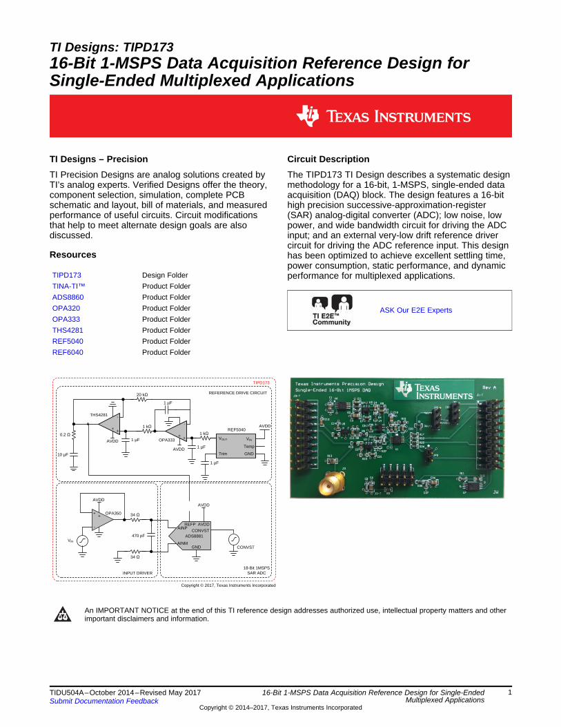
INPUT DRIVER
REFERENCE DRIVE CIRCUIT
18-Bit 1MSPS SAR ADC
REF5040
TIPD173
1 µF
1 N�
1 µF
1 µF
VOUT VIN
Temp
GNDTrim
AVDD
Copyright © 2017, Texas Instruments Incorporated
1TIDU504A–October 2014–Revised May 2017Submit Documentation Feedback
Copyright © 2014–2017, Texas Instruments Incorporated
16-Bit 1-MSPS Data Acquisition Reference Design for Single-EndedMultiplexed Applications
TI Designs: TIPD17316-Bit 1-MSPS Data Acquisition Reference Design forSingle-Ended Multiplexed Applications
TI Designs – PrecisionTI Precision Designs are analog solutions created byTI’s analog experts. Verified Designs offer the theory,component selection, simulation, complete PCBschematic and layout, bill of materials, and measuredperformance of useful circuits. Circuit modificationsthat help to meet alternate design goals are alsodiscussed.
Resources
TIPD173 Design FolderTINA-TI™ Product FolderADS8860 Product FolderOPA320 Product FolderOPA333 Product FolderTHS4281 Product FolderREF5040 Product FolderREF6040 Product Folder
Circuit DescriptionThe TIPD173 TI Design describes a systematic designmethodology for a 16-bit, 1-MSPS, single-ended dataacquisition (DAQ) block. The design features a 16-bithigh precision successive-approximation-register(SAR) analog-digital converter (ADC); low noise, lowpower, and wide bandwidth circuit for driving the ADCinput; and an external very-low drift reference drivercircuit for driving the ADC reference input. This designhas been optimized to achieve excellent settling time,power consumption, static performance, and dynamicperformance for multiplexed applications.
ASK Our E2E Experts
An IMPORTANT NOTICE at the end of this TI reference design addresses authorized use, intellectual property matters and otherimportant disclaimers and information.
Time (ns)
Dig
ital C
ode
(LS
B)
700 800 900 1000 1100 1200 130065519.0
65519.5
65520.0
65520.5
65521.0
65521.5
65522.0
65522.5
D001Time (ns)
Dig
ital C
ode
(LS
B)
700 800 900 1000 1100 1200 13001297.0
1297.5
1298.0
1298.5
1299.0
1299.5
1300.0
1300.5
1301.0
D002
Error Band within 1LSB
Error Band within 1LSB
System Overview www.ti.com
2 TIDU504A–October 2014–Revised May 2017Submit Documentation Feedback
Copyright © 2014–2017, Texas Instruments Incorporated
16-Bit 1-MSPS Data Acquisition Reference Design for Single-EndedMultiplexed Applications
1 System Overview
1.1 Design SummaryThe primary objective for this design is to create a 16-bit, 1-MSPS, single-ended DAQ system that isoptimized to achieve excellent transient settling performance for a full-scale step input signal. The designrequirements for this block design are as follows:• System supply voltage: 5-V DC• ADC supply voltage: 3.3-V DC• ADC sampling rate: 1 MSPS• ADC reference voltage: 4.096-V DC• ADC input signal range: A step input range from 0.1 V to VREF. The system does not utilize a negative
supply; therefore, the minimum input signal is limited by the input output limitation of the operationalamplifier (op amp) to avoid any signal distortion.
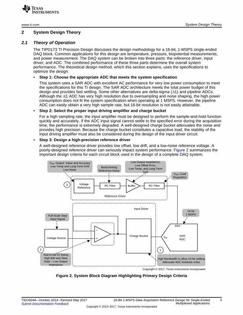
1.2 Key System SpecificationsTable 1 summarizes the design goals and performance. Figure 1 shows the system specificationcontaining the low power, fast settling time, static performance, and dynamic performance.
(1) The 16-bit settling time starts when the multiplexer changes the channel.(2) The signal-to-noise ratio (SNR) and settling time are the most important performance trade-offs addressed in this design. If a
low-cutoff-frequency input filter is implemented to achieve lower noise, the large RC time constant results in longer settling timeand vice versa.
Table 1. Comparison of Design Goals, Simulation, and Measured Performance
PARAMETERS SPECIFICATION SIMULATION MEASUREDTotal power ≤ 25 mW — 21.5 mW
16-bit settling time (1) ≤ 900 ns 852 ns 850 nsEffective resolutionSYS 16 bits — 16 bits
Linearity error < ±2 LSB — < ±0.5 LSBSignal-to-noise ratioSYS (SNRSYS) (2) > 90 dB — 90.5 dB
Total harmonic distortionSYS (THDSYS) < –104 dB — –105.4 dBEffective number of bitsSYS (ENOBSYS) > 14.5 bits — 14.58 dB
(1) Each test measurement in Figure 1 includes an average of 1000 data points to reduce the noise.
Figure 1 shows the resulting measured data for the worst-case scenario, which is the multiplexer switchingchannels having the input swing form the negative rail to the positive, and vice versa.
Figure 1. Measurement Result of Settling Time Plot for Multiplexed Data Acquisition Block (1)
Rising Full-Scale Input and Falling Full-Scale Input
+SARADC
BufferVoltageReference
RC Filter RC Filter
Input Driver
Reference Driver
VREF Output: Value and AccuracyLow Temp and Long-Term Drift
Low NoiseBand-limiting
Reference Noise
Low Output Impedance,Low Offset Error,
Low Temp, and Long-Term Drift
VREF Load Regulation
16 bit1 MSPS
REF
VIN
Full-Scale Step Input Signal
High Bandwidth to allow 16-bit settlingAttenuate ADC kickback noise
Charge Bucket
Rail-to-rail IO SwingHigh BW and Slew Rate ± Low Output
Impedance
Voltage Source
12
3
±
Copyright © 2017, Texas Instruments Incorporated
www.ti.com System Design Theory
3TIDU504A–October 2014–Revised May 2017Submit Documentation Feedback
Copyright © 2014–2017, Texas Instruments Incorporated
16-Bit 1-MSPS Data Acquisition Reference Design for Single-EndedMultiplexed Applications
2 System Design Theory
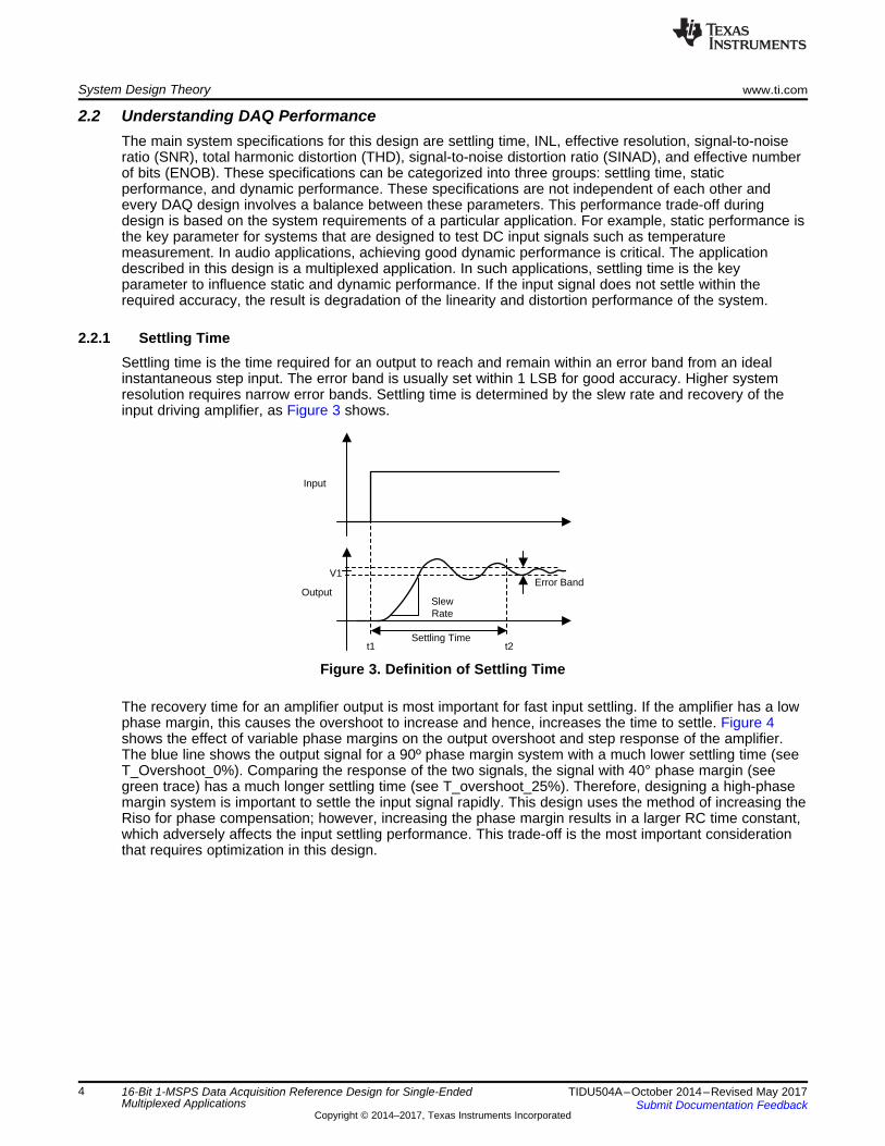
2.1 Theory of OperationThe TIPD173 TI Precision Design discusses the design methodology for a 16-bit, 1-MSPS single-endedDAQ block. Common applications for this design are temperature, pressure, biopotential measurements,and power measurement. The DAQ system can be broken into three parts: the reference driver, inputdriver, and ADC. The combined performance of these three parts determine the overall systemperformance. The theoretical design method, which this section explains, uses the specifications tooptimize the design.• Step 1: Choose the appropriate ADC that meets the system specification
This system uses a SAR ADC with excellent AC performance for very low power consumption to meetthe specifications for this TI design. The SAR ADC architecture meets the total power budget of thisdesign and provides fast settling. Some other alternatives are delta-sigma (ΔΣ) and pipeline ADCs.Although the ΔΣ ADC has very high resolution due to oversampling and noise shaping, the high powerconsumption does not fit the system specification when operating at 1 MSPS. However, the pipelineADC can easily obtain a very high sample rate, but 16-bit resolution is not easily attainable.
• Step 2: Select the proper input driving amplifier and charge bucketFor a high sampling rate, the input amplifier must be designed to perform the sample-and-hold functionquickly and accurately. If the ADC input signal cannot settle to the specified error during the acquisitiontime, the performance is extremely degraded. A well-designed charge bucket attenuates the noise andprovides high precision. Because the charge bucket constitutes a capacitive load, the stability of theinput driving amplifier must also be considered during the design of the input driver circuit.
• Step 3: Design a high-precision reference driverA well-designed reference driver provides low offset, low drift, and a low-noise reference voltage. Apoorly-designed reference driver can seriously impact system performance. Figure 2 summarizes theimportant design criteria for each circuit block used in the design of a complete DAQ system.
Figure 2. System Block Diagram Highlighting Primary Design Criteria
Input
Output
V1
t1 t2
Error Band
Settling Time
Slew Rate
System Design Theory www.ti.com
4 TIDU504A–October 2014–Revised May 2017Submit Documentation Feedback
Copyright © 2014–2017, Texas Instruments Incorporated
16-Bit 1-MSPS Data Acquisition Reference Design for Single-EndedMultiplexed Applications
2.2 Understanding DAQ PerformanceThe main system specifications for this design are settling time, INL, effective resolution, signal-to-noiseratio (SNR), total harmonic distortion (THD), signal-to-noise distortion ratio (SINAD), and effective numberof bits (ENOB). These specifications can be categorized into three groups: settling time, staticperformance, and dynamic performance. These specifications are not independent of each other andevery DAQ design involves a balance between these parameters. This performance trade-off duringdesign is based on the system requirements of a particular application. For example, static performance isthe key parameter for systems that are designed to test DC input signals such as temperaturemeasurement. In audio applications, achieving good dynamic performance is critical. The applicationdescribed in this design is a multiplexed application. In such applications, settling time is the keyparameter to influence static and dynamic performance. If the input signal does not settle within therequired accuracy, the result is degradation of the linearity and distortion performance of the system.
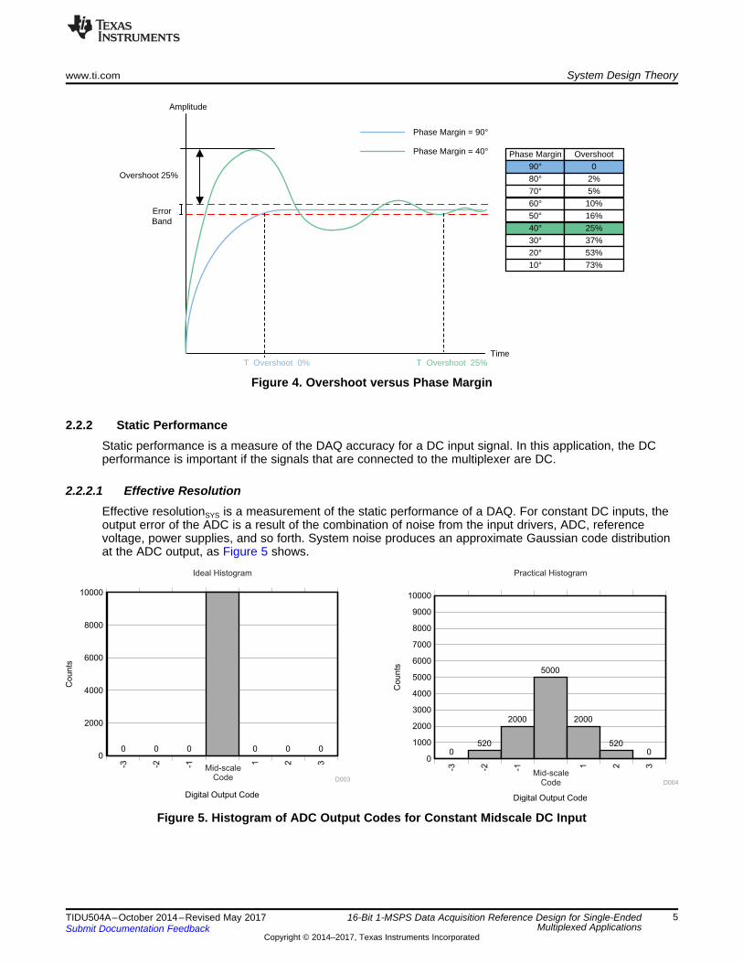
2.2.1 Settling TimeSettling time is the time required for an output to reach and remain within an error band from an idealinstantaneous step input. The error band is usually set within 1 LSB for good accuracy. Higher systemresolution requires narrow error bands. Settling time is determined by the slew rate and recovery of theinput driving amplifier, as Figure 3 shows.
Figure 3. Definition of Settling Time
The recovery time for an amplifier output is most important for fast input settling. If the amplifier has a lowphase margin, this causes the overshoot to increase and hence, increases the time to settle. Figure 4shows the effect of variable phase margins on the output overshoot and step response of the amplifier.The blue line shows the output signal for a 90º phase margin system with a much lower settling time (seeT_Overshoot_0%). Comparing the response of the two signals, the signal with 40° phase margin (seegreen trace) has a much longer settling time (see T_overshoot_25%). Therefore, designing a high-phasemargin system is important to settle the input signal rapidly. This design uses the method of increasing theRiso for phase compensation; however, increasing the phase margin results in a larger RC time constant,which adversely affects the input settling performance. This trade-off is the most important considerationthat requires optimization in this design.
Digital Output Code
Co
un
ts
0
2000
4000
6000
8000
10000
-3 -2 -1 1 2 3
0 0 0 0 0 0
D003
Digital Output Code
Co
un
ts
0
1000
2000
3000
4000
5000
6000
7000
8000
9000
10000
-3 -2 -1 1 2 3
0520
2000
5000
2000
5200
D004
Mid-scaleCode
Mid-scaleCode
Ideal Histogram Practical Histogram
Amplitude
TimeT_Overshoot_0% T_Overshoot_25%
Overshoot 25%
Phase Margin = 90°
Phase Margin = 40°
Error Band
Phase Margin Overshoot
90° 0
80° 2%
70° 5%
60° 10%
50° 16%
40° 25%
30° 37%
20° 53%
10° 73%
www.ti.com System Design Theory
5TIDU504A–October 2014–Revised May 2017Submit Documentation Feedback
Copyright © 2014–2017, Texas Instruments Incorporated
16-Bit 1-MSPS Data Acquisition Reference Design for Single-EndedMultiplexed Applications
Figure 4. Overshoot versus Phase Margin
2.2.2 Static PerformanceStatic performance is a measure of the DAQ accuracy for a DC input signal. In this application, the DCperformance is important if the signals that are connected to the multiplexer are DC.
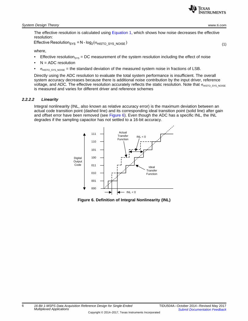
2.2.2.1 Effective ResolutionEffective resolutionSYS is a measurement of the static performance of a DAQ. For constant DC inputs, theoutput error of the ADC is a result of the combination of noise from the input drivers, ADC, referencevoltage, power supplies, and so forth. System noise produces an approximate Gaussian code distributionat the ADC output, as Figure 5 shows.
Figure 5. Histogram of ADC Output Codes for Constant Midscale DC Input
111
110
100
011
010
001
000
101
Digital Output Code
IdealTransferFunction
ActualTransferFunction
INL < 0
INL < 0
SYS 2 HISTO_SYS_NOISEEffective Resolution = N - log ( )s
System Design Theory www.ti.com
6 TIDU504A–October 2014–Revised May 2017Submit Documentation Feedback
Copyright © 2014–2017, Texas Instruments Incorporated
16-Bit 1-MSPS Data Acquisition Reference Design for Single-EndedMultiplexed Applications
The effective resolution is calculated using Equation 1, which shows how noise decreases the effectiveresolution:
(1)
where,• Effective resolutionSYS = DC measurement of the system resolution including the effect of noise• N = ADC resolution• σHISTO_SYS_NOISE = the standard deviation of the measured system noise in fractions of LSB.
Directly using the ADC resolution to evaluate the total system performance is insufficient. The overallsystem accuracy decreases because there is additional noise contribution by the input driver, referencevoltage, and ADC. The effective resolution accurately reflects the static resolution. Note that σHISTO_SYS_NOISEis measured and varies for different driver and reference schemes
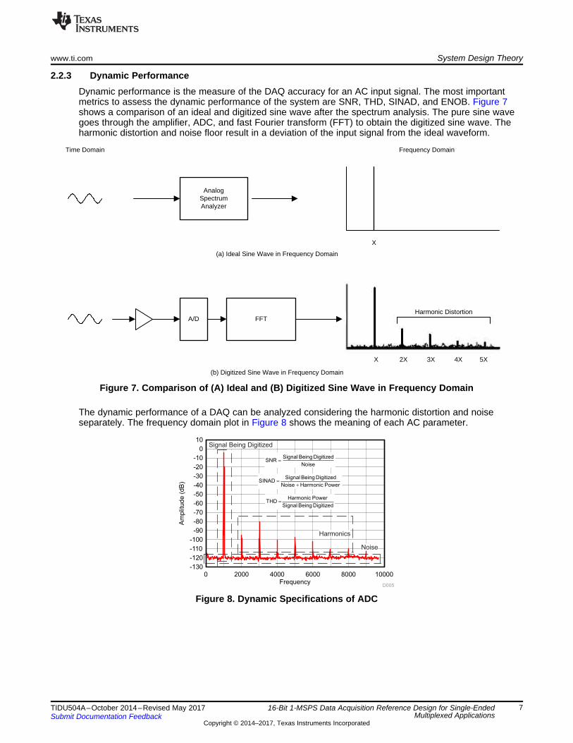
2.2.2.2 LinearityIntegral nonlinearity (INL, also known as relative accuracy error) is the maximum deviation between anactual code transition point (dashed line) and its corresponding ideal transition point (solid line) after gainand offset error have been removed (see Figure 6). Even though the ADC has a specific INL, the INLdegrades if the sampling capacitor has not settled to a 16-bit accuracy.
Figure 6. Definition of Integral Nonlinearity (INL)
Frequency
Am
plit
ud
e(d
B)
0 2000 4000 6000 8000 10000-130
-120
-110
-100
-90
-80
-70
-60
-50
-40
-30
-20
-10
0
10
D005
Noise
Harmonics
Signal Being Digitized
Signal Being DigitizedSNR
Noise=
Signal Being DigitizedSINAD
Noise Harmonic Power=
+
Harmonic PowerTHD
Signal Being Digitized=
(a) Ideal Sine Wave in Frequency Domain
(b) Digitized Sine Wave in Frequency Domain
Frequency Domain
X
AnalogSpectrumAnalyzer
Time Domain
A/D FFT
X 2X 3X 4X 5X
Harmonic Distortion
www.ti.com System Design Theory
7TIDU504A–October 2014–Revised May 2017Submit Documentation Feedback
Copyright © 2014–2017, Texas Instruments Incorporated
16-Bit 1-MSPS Data Acquisition Reference Design for Single-EndedMultiplexed Applications
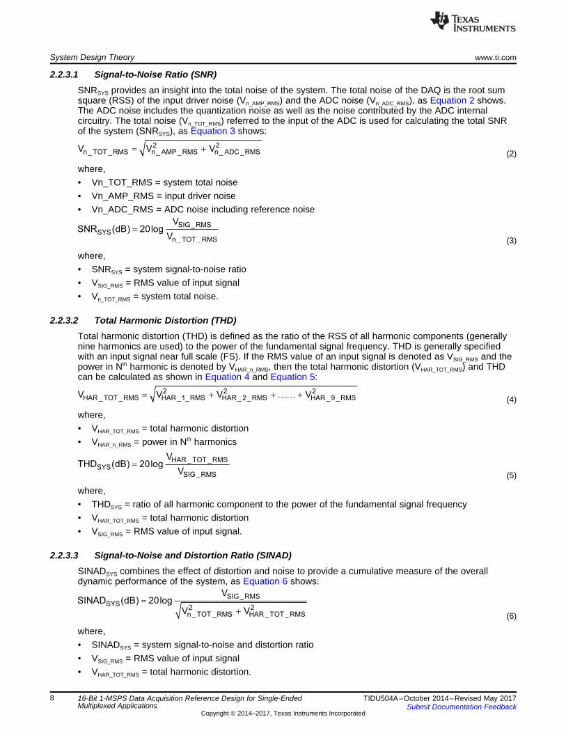
2.2.3 Dynamic PerformanceDynamic performance is the measure of the DAQ accuracy for an AC input signal. The most importantmetrics to assess the dynamic performance of the system are SNR, THD, SINAD, and ENOB. Figure 7shows a comparison of an ideal and digitized sine wave after the spectrum analysis. The pure sine wavegoes through the amplifier, ADC, and fast Fourier transform (FFT) to obtain the digitized sine wave. Theharmonic distortion and noise floor result in a deviation of the input signal from the ideal waveform.
Figure 7. Comparison of (A) Ideal and (B) Digitized Sine Wave in Frequency Domain
The dynamic performance of a DAQ can be analyzed considering the harmonic distortion and noiseseparately. The frequency domain plot in Figure 8 shows the meaning of each AC parameter.
Figure 8. Dynamic Specifications of ADC
SIG_RMSSYS
2 2n_ TOT _RMS HAR _ TOT _RMS
VSINAD (dB) 20log
V V=
+
HAR _ TOT _RMSSYS
SIG_RMS
VTHD (dB) 20log
V=
2 2 2HAR _ TOT _RMS HAR _1_RMS HAR _ 2_RMS HAR _9 _RMSV V V V= + + +KK
SIG_RMSSYS
n_ TOT _RMS
VSNR (dB) 20log
V=
2 2n_ TOT _RMS n_ AMP _RMS n_ ADC_RMSV V V= +
System Design Theory www.ti.com
8 TIDU504A–October 2014–Revised May 2017Submit Documentation Feedback
Copyright © 2014–2017, Texas Instruments Incorporated
16-Bit 1-MSPS Data Acquisition Reference Design for Single-EndedMultiplexed Applications
2.2.3.1 Signal-to-Noise Ratio (SNR)SNRSYS provides an insight into the total noise of the system. The total noise of the DAQ is the root sumsquare (RSS) of the input driver noise (Vn_AMP_RMS) and the ADC noise (Vn_ADC_RMS), as Equation 2 shows.The ADC noise includes the quantization noise as well as the noise contributed by the ADC internalcircuitry. The total noise (Vn_TOT_RMS) referred to the input of the ADC is used for calculating the total SNRof the system (SNRSYS), as Equation 3 shows:
(2)
where,• Vn_TOT_RMS = system total noise• Vn_AMP_RMS = input driver noise• Vn_ADC_RMS = ADC noise including reference noise
(3)
where,• SNRSYS = system signal-to-noise ratio• VSIG_RMS = RMS value of input signal• Vn_TOT_RMS = system total noise.
2.2.3.2 Total Harmonic Distortion (THD)Total harmonic distortion (THD) is defined as the ratio of the RSS of all harmonic components (generallynine harmonics are used) to the power of the fundamental signal frequency. THD is generally specifiedwith an input signal near full scale (FS). If the RMS value of an input signal is denoted as VSIG_RMS and thepower in Nth harmonic is denoted by VHAR_n_RMS, then the total harmonic distortion (VHAR_TOT_RMS) and THDcan be calculated as shown in Equation 4 and Equation 5:
(4)
where,• VHAR_TOT_RMS = total harmonic distortion• VHAR_n_RMS = power in Nth harmonics
(5)
where,• THDSYS = ratio of all harmonic component to the power of the fundamental signal frequency• VHAR_TOT_RMS = total harmonic distortion• VSIG_RMS = RMS value of input signal.
2.2.3.3 Signal-to-Noise and Distortion Ratio (SINAD)SINADSYS combines the effect of distortion and noise to provide a cumulative measure of the overalldynamic performance of the system, as Equation 6 shows:
(6)
where,• SINADSYS = system signal-to-noise and distortion ratio• VSIG_RMS = RMS value of input signal• VHAR_TOT_RMS = total harmonic distortion.
SYSSYS
SINAD 1.76ENOB
6.02
-
=
www.ti.com System Design Theory
9TIDU504A–October 2014–Revised May 2017Submit Documentation Feedback
Copyright © 2014–2017, Texas Instruments Incorporated
16-Bit 1-MSPS Data Acquisition Reference Design for Single-EndedMultiplexed Applications
2.2.3.4 Effective Number of Bits (ENOB)ENOBSYS is an effective measurement of the quality of a digitized signal from an ADC by specifying thenumber of bits above the noise floor (see Equation 7):
(7)
where,• SINADSYS = system signal-to-noise and distribution ratio• ENOBSYS = effective number of bits.
2.3 Design Consideration of DAQ for Multiplexed ApplicationThe primary design consideration for a multiplexed application is settling time. If the settling time is toolarge such that the signal cannot converge within the specified error band, then errors occur that aregreater than the expected device errors. The error affects both static and dynamic performance. Thisdesign is based on the worst-case scenario which is switching between different channels, where onechannel is at the negative full-scale (NFS) voltage and the other channel is at the positive full-scale (PFS)voltage. In this case, the step size is the full-scale range (FSR); therefore, the input driver requires thelongest time to settle within the error band. The time it takes to change channels also affects the settlingtime of the system.
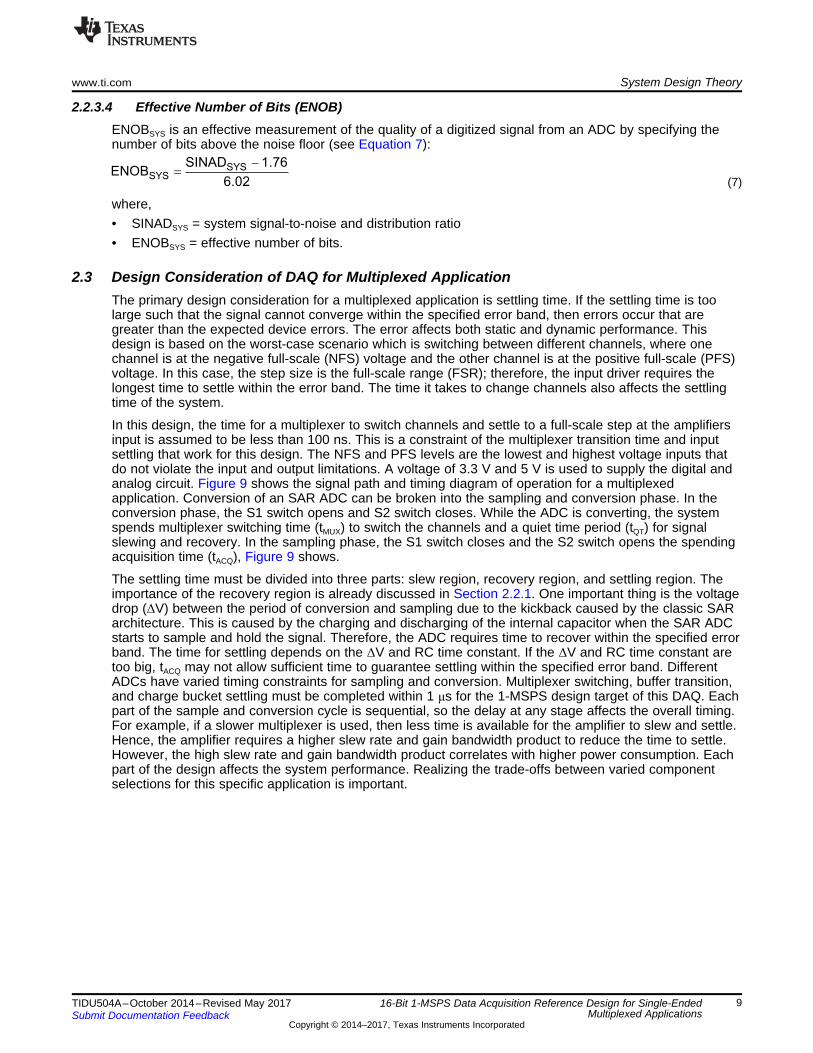
In this design, the time for a multiplexer to switch channels and settle to a full-scale step at the amplifiersinput is assumed to be less than 100 ns. This is a constraint of the multiplexer transition time and inputsettling that work for this design. The NFS and PFS levels are the lowest and highest voltage inputs thatdo not violate the input and output limitations. A voltage of 3.3 V and 5 V is used to supply the digital andanalog circuit. Figure 9 shows the signal path and timing diagram of operation for a multiplexedapplication. Conversion of an SAR ADC can be broken into the sampling and conversion phase. In theconversion phase, the S1 switch opens and S2 switch closes. While the ADC is converting, the systemspends multiplexer switching time (tMUX) to switch the channels and a quiet time period (tQT) for signalslewing and recovery. In the sampling phase, the S1 switch closes and the S2 switch opens the spendingacquisition time (tACQ), Figure 9 shows.
The settling time must be divided into three parts: slew region, recovery region, and settling region. Theimportance of the recovery region is already discussed in Section 2.2.1. One important thing is the voltagedrop (ΔV) between the period of conversion and sampling due to the kickback caused by the classic SARarchitecture. This is caused by the charging and discharging of the internal capacitor when the SAR ADCstarts to sample and hold the signal. Therefore, the ADC requires time to recover within the specified errorband. The time for settling depends on the ΔV and RC time constant. If the ΔV and RC time constant aretoo big, tACQ may not allow sufficient time to guarantee settling within the specified error band. DifferentADCs have varied timing constraints for sampling and conversion. Multiplexer switching, buffer transition,and charge bucket settling must be completed within 1 μs for the 1-MSPS design target of this DAQ. Eachpart of the sample and conversion cycle is sequential, so the delay at any stage affects the overall timing.For example, if a slower multiplexer is used, then less time is available for the amplifier to slew and settle.Hence, the amplifier requires a higher slew rate and gain bandwidth product to reduce the time to settle.However, the high slew rate and gain bandwidth product correlates with higher power consumption. Eachpart of the design affects the system performance. Realizing the trade-offs between varied componentselections for this specific application is important.
VADC_IN
Slewing
Recovery
tQT tACQ
Slew rate
VREF
Settling
LSB
¨9
VNFS VPFS
Positive Full Scale
Negative Full Scale
MUX
VNFS
VPFS
+
VFSR
Full-ScaleRange
VIN (t)
SAR ADC
VADC_IN
CONVST
CONVERSION SAMPLING
TCYC_MIN = 1 µs
VADC_IN
tQT tACQ
SlewingRecovery
VIN
tMUX = TCYC_MIN ± (tQT + tACQ)
Settling
RFLT
CFLT CSH
RSH
S1 S2
RO
Compartor
VREF
Digital Code
+
±+
±
¨9
System Design Theory www.ti.com
10 TIDU504A–October 2014–Revised May 2017Submit Documentation Feedback
Copyright © 2014–2017, Texas Instruments Incorporated
16-Bit 1-MSPS Data Acquisition Reference Design for Single-EndedMultiplexed Applications
Figure 9. Timing Diagram of Settling Time in DAQ
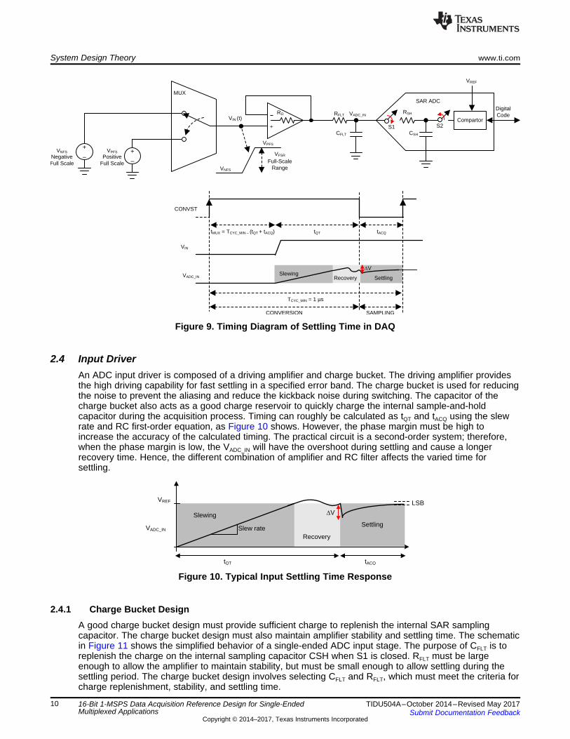
2.4 Input DriverAn ADC input driver is composed of a driving amplifier and charge bucket. The driving amplifier providesthe high driving capability for fast settling in a specified error band. The charge bucket is used for reducingthe noise to prevent the aliasing and reduce the kickback noise during switching. The capacitor of thecharge bucket also acts as a good charge reservoir to quickly charge the internal sample-and-holdcapacitor during the acquisition process. Timing can roughly be calculated as tQT and tACQ using the slewrate and RC first-order equation, as Figure 10 shows. However, the phase margin must be high toincrease the accuracy of the calculated timing. The practical circuit is a second-order system; therefore,when the phase margin is low, the VADC_IN will have the overshoot during settling and cause a longerrecovery time. Hence, the different combination of amplifier and RC filter affects the varied time forsettling.
Figure 10. Typical Input Settling Time Response
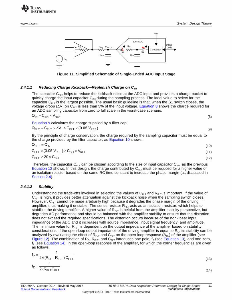
2.4.1 Charge Bucket DesignA good charge bucket design must provide sufficient charge to replenish the internal SAR samplingcapacitor. The charge bucket design must also maintain amplifier stability and settling time. The schematicin Figure 11 shows the simplified behavior of a single-ended ADC input stage. The purpose of CFLT is toreplenish the charge on the internal sampling capacitor CSH when S1 is closed. RFLT must be largeenough to allow the amplifier to maintain stability, but must be small enough to allow settling during thesettling period. The charge bucket design involves selecting CFLT and RFLT, which must meet the criteria forcharge replenishment, stability, and settling time.
Z
FLT FLT
1f
2 R C=
p
PO FLT FLT
1f
2 (R R ) C=
p +
FLT SHC 20 C³ ´
FLT REF SH REFC (0.05 V ) C V´ ³ ´
FLT INQ Q=
FLT FLT FLT REFQ C V C (0.05 V )= ´ D £ ´
IN SH REFQ C V= ´
VIN
+
SAR ADC
VADC_INRFLT
CFLT CSH
RSH
S1 S2
RO
Compartor
VREF
Digital Code
www.ti.com System Design Theory
11TIDU504A–October 2014–Revised May 2017Submit Documentation Feedback
Copyright © 2014–2017, Texas Instruments Incorporated
16-Bit 1-MSPS Data Acquisition Reference Design for Single-EndedMultiplexed Applications
Figure 11. Simplified Schematic of Single-Ended ADC Input Stage
2.4.1.1 Reducing Charge Kickback—Replenish Charge on CSH
The capacitor CFLT helps to reduce the kickback noise at the ADC input and provides a charge bucket toquickly charge the input capacitor CSH during the sampling process. The ideal value to select for thecapacitor CFLT is the largest possible. The usual basic guideline is that, when the S1 switch closes, thevoltage droop (ΔV) on CFLT is less than 5% of the input voltage. Equation 8 shows the charge required foran ADC sampling capacitor from zero to full scale in the worst-case scenario.
(8)
Equation 9 calculates the charge supplied by a filter cap:(9)
By the principle of charge conservation, the charge required by the sampling capacitor must be equal tothe charge provided by the filter capacitor, as Equation 10 shows.
(10)
(11)
(12)
Therefore, the capacitor CFLT can be chosen according to the size of input capacitor CSH, as the previousEquation 12 shows. In this design, the charge contributed by CFLT must be reduced for a higher value ofan isolation resistor based on the same RC time constant to increase the phase margin (as discussed inSection 2.4).
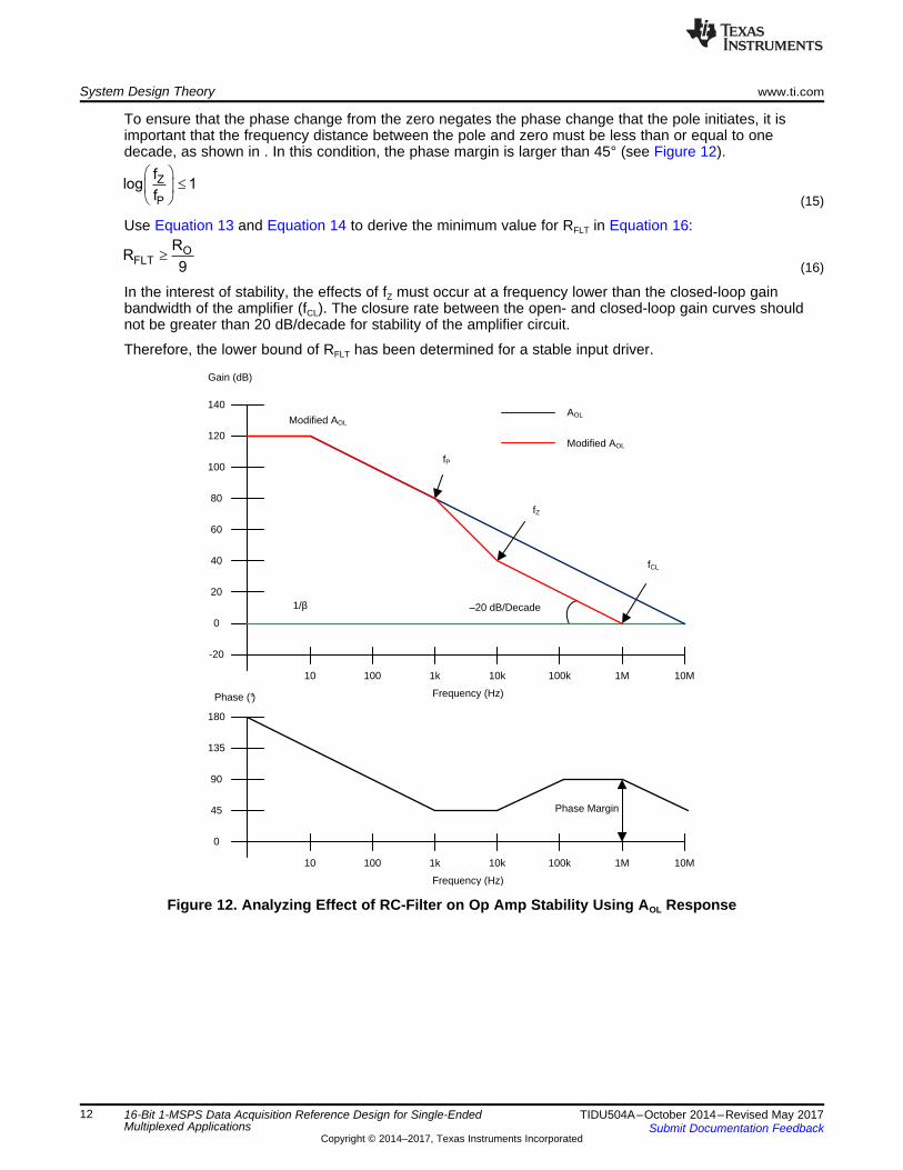
2.4.1.2 StabilityUnderstanding the trade-offs involved in selecting the values of CFLT and RFLT is important. If the value ofCFLT is high, it provides better attenuation against the kickback noise when the sampling switch closes.However, CFLT cannot be made arbitrarily high because it degrades the phase margin of the drivingamplifier, thus making it unstable. The series resistor RFLT acts as an isolation resistor, which helps tostabilize the driving amplifier. A higher value of RFLT is helpful from the amplifier stability perspective, butdegrades AC performance and should be balanced with the amplifier stability to ensure that the distortiondoes not exceed the required specifications. The distortion occurs because of the non-linear inputimpedance of the ADC and it increases with source impedance, input signal frequency, and amplitude.The minimum value for RFLT is dependent on the output impedance of the amplifier based on stabilityconsiderations. If the open-loop output impedance of the driving amplifier is equal to RO, its stability can beanalyzed by evaluating the effect of RFLT and CFLT on the open-loop response (AOL) of the amplifier (seeFigure 12). The combination of RO, RFLT, and CFLT introduces one pole, fP (see Equation 13), and one zero,fZ (see Equation 14), in the open-loop response of the amplifier, for which the corner frequencies are givenas follows:
(13)
(14)
fP
fZ
fCL
Modified AOL
1/� ±20 dB/Decade
10 100
-20
0
20
40
60
80
100
120
140
1k 10k 100k 1M 10M
Gain (dB)
Frequency (Hz)
10 100
0
45
90
135
180
1k 10k 100k 1M 10M
Phase (°)
Frequency (Hz)
Phase Margin
AOL
Modified AOL
OFLT
RR
9³
Z
P
flog 1
f
æ ö£ç ÷
è ø
System Design Theory www.ti.com
12 TIDU504A–October 2014–Revised May 2017Submit Documentation Feedback
Copyright © 2014–2017, Texas Instruments Incorporated
16-Bit 1-MSPS Data Acquisition Reference Design for Single-EndedMultiplexed Applications
To ensure that the phase change from the zero negates the phase change that the pole initiates, it isimportant that the frequency distance between the pole and zero must be less than or equal to onedecade, as shown in . In this condition, the phase margin is larger than 45° (see Figure 12).
(15)
Use Equation 13 and Equation 14 to derive the minimum value for RFLT in Equation 16:
(16)
In the interest of stability, the effects of fZ must occur at a frequency lower than the closed-loop gainbandwidth of the amplifier (fCL). The closure rate between the open- and closed-loop gain curves shouldnot be greater than 20 dB/decade for stability of the amplifier circuit.
Therefore, the lower bound of RFLT has been determined for a stable input driver.
Figure 12. Analyzing Effect of RC-Filter on Op Amp Stability Using AOL Response
OFLT
FLT
R tR
V9ln C
1LSB
£ £Dæ ö
´ç ÷è ø
FLT SHC 20 C³ ´
FLT
FLT
tR
Vln C
1LSB
£Dæ ö
´ç ÷è ø
FLT FLT
VR C ln( ) t
1LSB
D´ ´ £
t
Ve
1LSB
tD
£
t
V e 1LSB-
tD ´ £
t( )
REF REFV (V V e ) 1LSB-
t- - D ´ £
REF ADC_INV V (t) 1LSB- £
t
ADC_IN REFV (t) V V e
æ ö-ç ÷tè ø= - D ´
www.ti.com System Design Theory
13TIDU504A–October 2014–Revised May 2017Submit Documentation Feedback
Copyright © 2014–2017, Texas Instruments Incorporated
16-Bit 1-MSPS Data Acquisition Reference Design for Single-EndedMultiplexed Applications
2.4.1.3 Settling TimeA fast settling time with inputs settling within 1 LSB is necessary to maintain good linearity. The worstcase is that the input voltage VIN changes by a full-scale step from 0.1 V to VREF, but the CFLT provides acharge bucket. The voltage drop can be calculated using Equation 9. Therefore, the behavior of the inputvoltage is represented by Equation 17:
(17)
where,• τ = RFLT × CFLT
• t = tACQ = acquisition time• ΔV = CSH × VREF / CFLT.
For a specific sampling time, the RC time constant must be designed to meet the timing and accuracyconstraint as Equation 18 shows. The following equation can be derived from Equation 18 to Equation 23:
(18)
(19)
(20)
(21)
(22)
(23)
where,• 1 LSB = VREF / 2N.
Therefore, the upper bound of RFLT has been determined for the settling time as shown in Equation 23.
Notice that Equation 18 is based on the assumption that the ADC input has already settled to VREF (seeFigure 10). In this design, to satisfy the assumption, RFLT needs to increase the phase margin and must beselected close to the upper bound to ensure settling to VREF, because the selected input driver only hassufficient bandwidth for a low power specification. If the ADC input has not settled before the sampling-and-hold region, the V_ADC_IN must be adjusted to other values.
2.4.1.4 Final Selection of RFLT and CFLT—Check Stability and Settling Time CriteriaThe value of the charge bucket can be summarized by checking stability and settling time, as Equation 24and Equation 25 show.
(24)
(25)
The first step is to select the CFLT based on Equation 24. Then choose the lower bound RFLT value andcheck the settling time and phase margin. If the settling time is too long because of phase margin, selectthe upper bound value of RFLT and recheck the settling time and phase margin. If the phase margin is stillnot enough, CFLT must be adjusted to a smaller value due to the higher value of RFLT, which increases thephase margin based on the same RC time constant.
Notice that the practical circuit is the second-order system; therefore, increasing RFLT does not mean thatthe settling time will increase.
SH REFOUT
FLT FLT
C VI
C R
´³
´
FLTOUT
FLT
VI
R
D³
FLT FLT
1Unity Gain Bandwidth 4
2 R C- ³ ´
p
OUTVSlew Rate MAX( )
t
D=
D
System Design Theory www.ti.com
14 TIDU504A–October 2014–Revised May 2017Submit Documentation Feedback
Copyright © 2014–2017, Texas Instruments Incorporated
16-Bit 1-MSPS Data Acquisition Reference Design for Single-EndedMultiplexed Applications
2.4.2 Input Amplifier DesignAnother key aspect in designing the input driver circuit for high-resolution SAR ADCs is the selection of anappropriate driving amplifier. The amplifier selection process is highly dependent on the input signal andthroughput of the ADC. This design is optimized for a full-scale step input signal, so the key amplifierspecifications for the selection criteria are as follows.
2.4.2.1 Slew RateThe minimum slew rate for the driving amplifier is dependent on the type and amplitude of the input signal(see Equation 26):
(26)
where,• Δt = tQT = quiet time period• ΔVOUT = VREF = reference voltage.
2.4.2.2 BandwidthThis bandwidth must be much higher than the bandwidth of the ADC input circuit to ensure that there is noattenuation of the input signal resulting from the bandwidth limitation of the amplifier. In general, select theamplifier based on the calculation in Equation 27.
(27)
2.4.2.3 Rail-to-Rail Input and Output SwingThis application uses an input signal with a full-scale voltage swing; therefore, an amplifier with support fora rail-to-rail input and output (RRIO) swing is required.
2.4.2.4 Open-Loop Output ImpedanceThe output impedance must be as low as possible to efficiently drive the switched capacitor inputs of theSAR ADC as well as to maintain the op amp stability under high capacitive load conditions.
2.4.2.5 Max Output CurrentThe output peak current drive requirement for the amplifier is dependent on the values of RFLT and CFLT.This dependency is due to the fact that, during sampling, the capacitor CFLT charges the internal samplingcapacitor (CSH), which causes a voltage drop across CFLT. The recharge current for capacitor CFLT isprovided by the output stage of the amplifier, thus imposing a minimum condition on the output drivecapability of the amplifier as calculated by Equation 28 and Equation 29.
(28)
(29)
2.4.2.6 Offset DriftThe offset drift is an important parameter used to influence the accuracy. The output error is caused bytemperature variation. In industrial applications, the wide temperature range environment is common;therefore, the amplifier drift must be as low as possible to ensure good performance.
n_ AMP _RMS n_ AMP _RTI_RMS
FLT n_ AMP _DENSITY
FLT n_ AMP _DENSITY
V Noise Gain V
Noise Gain 1.57 BW V
1.57 BW V
= ´
= ´ ´ ´
= ´ ´
+
VIN
VOUT**
*
*
: Voltage Noise Source
: Current Noise Source
www.ti.com System Design Theory
15TIDU504A–October 2014–Revised May 2017Submit Documentation Feedback
Copyright © 2014–2017, Texas Instruments Incorporated
16-Bit 1-MSPS Data Acquisition Reference Design for Single-EndedMultiplexed Applications
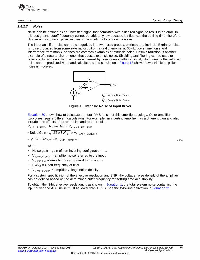
2.4.2.7 NoiseNoise can be defined as an unwanted signal that combines with a desired signal to result in an error. Inthis design, the cutoff frequency cannot be arbitrarily low because it influences the settling time; therefore,choose a low-noise amplifier as one of the solutions to reduce the noise.
The input amplifier noise can be categorized into two basic groups: extrinsic and intrinsic. Extrinsic noiseis noise produced from some external circuit or natural phenomena. 60-Hz power line noise andinterference from mobile phones are common examples of extrinsic noise. Cosmic radiation is anotherexample of a natural phenomenon that causes extrinsic noise. Shielding and filtering can be used toreduce extrinsic noise. Intrinsic noise is caused by components within a circuit, which means that intrinsicnoise can be predicted with hand calculations and simulations. Figure 13 shows how intrinsic amplifiernoise is modeled.
Figure 13. Intrinsic Noise of Input Driver
Equation 30 shows how to calculate the total RMS noise for this amplifier topology. Other amplifiertopologies require different calculations. For example, an inverting amplifier has a different gain and alsoincludes the effects of current noise and resistor noise.
(30)
where,• Noise gain = gain of non-inverting configuration = 1• Vn_AMP_RTI_RMS = amplifier noise referred to the input• Vn_AMP_RMS = amplifier noise referred to the output• BWFLT = cutoff frequency of filter• Vn_AMP_DENSITY = amplifier voltage noise density.
For a system specification of the effective resolution and SNR, the voltage noise density of the amplifiercan be defined based on the determined cutoff frequency for settling time and stability.
To obtain the N-bit effective resolutionSYS as shown in Equation 1, the total system noise containing theinput driver and ADC noise must be lower than 1 LSB. See the following derivation in Equation 31.
( ) ( )
( )
SYS 2 HISTO_SYS_NOISE
SYS
2 HISTO_SYS_NOISE
HISTO_SYS_NOISE
2 2
HISTO_AMP_NOISE HISTO_ADC_NOISE
2HISTO_AMP_NOISE HISTO_ADC_
Effective Resolution = N - log ( )
For effective resolution N 16
log ( ) 0
1LSB
1LSB
1LSB
s
= =
Þ s £
Þ s £
Þ s + s £
Þ s £ - s( )
( ) ( )
( ) ( )
( ) ( )
2
NOISE
N22
n_ AMP _RMS HISTO_ADC_NOISEREF
22 REFn_ AMP _RMS HISTO_ADC_NOISE N
22HISTO_ADC_NOISE REF
n_ AMP _DENSITY NFLT
2V 1LSB
V
VV 1LSB
2
1LSB VV
1.57 BW 2
Þ ´ £ - s
Þ £ - s ´
- s ´£
´ ´
System Design Theory www.ti.com
16 TIDU504A–October 2014–Revised May 2017Submit Documentation Feedback
Copyright © 2014–2017, Texas Instruments Incorporated
16-Bit 1-MSPS Data Acquisition Reference Design for Single-EndedMultiplexed Applications
To achieve the target effective resolution, the σHISTO_AMP_NOISE must be lower than specified noise; therefore,after rearranging the equation, transforming the unit of noise can result in the noise density at existingparameters (see Equation 31):
(31)
where,• N = ADC resolution• σHISTO_SYS_NOISE = standard deviation of the measured system noise in fractions of LSB• σHISTO_AMP_NOISE = standard deviation of the measured amplifier noise in fractions of LSB• σHISTO_ADC_NOISE = standard deviation of the measured ADC noise in fractions of LSB; transition noise in
ADC datasheet• BWFLT = cutoff frequency of the filter• Vn_AMP_RMS = amplifier noise referred to the output• Vn_AMP_DENSTY = amplifier voltage noise density.
SYS ADC
2 2
REF REFSNR (dB) SNR (dB)
20 20
n_ AMP _DENSITYFLT
V V
2 2 10 2 2 10V
1.57 BW
æ ö æ öç ÷ ç ÷
-ç ÷ ç ÷ç ÷ ç ÷
´ ´è ø è ø£
´
SYS ADC
2 2
REF REFn_ AMP _RMS SNR (dB) SNR (dB)
20 20
V VV
2 2 10 2 2 10
æ ö æ öç ÷ ç ÷
£ -ç ÷ ç ÷ç ÷ ç ÷
´ ´è ø è ø
( )SYS
2
2REF
n_ AMP _RMS n_ ADC_RMSSNR (dB)
20
VV V
2 2 10
æ öç ÷
£ -ç ÷ç ÷
´è ø
SYS
2 2 REFn_ AMP _RMS n_ ADC_RMS SNR (dB)
20
VV V
2 2 10
+ £
´
SYS
REFn_ TOT _RMS SNR (dB)
20
VV
2 2 10
£
´
REF
SYSn_ TOT _RMS
V
2 2SNR (dB) 20log
V
æ öç ÷ç ÷=ç ÷ç ÷è ø
www.ti.com System Design Theory
17TIDU504A–October 2014–Revised May 2017Submit Documentation Feedback
Copyright © 2014–2017, Texas Instruments Incorporated
16-Bit 1-MSPS Data Acquisition Reference Design for Single-EndedMultiplexed Applications
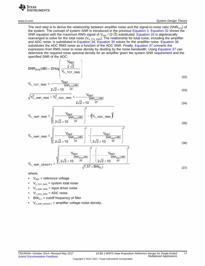
The next step is to derive the relationship between amplifier noise and the signal-to-noise ratio (SNRSYS) ofthe system. The concept of system SNR is introduced in the previous Equation 3. Equation 32 shows theSNR equation with the maximum RMS signal of VREF / (2√2) substituted. Equation 33 is algebraicallyrearranged to solve for the total noise (VN_TOT_RMS). The relationship for total noise, including the amplifierand ADC noise, is substituted in Equation 34. Equation 35 solves for the amplifier noise. Equation 36substitutes the ADC RMS noise as a function of the ADC SNR. Finally, Equation 37 converts theexpression from RMS noise to noise density by dividing by the noise bandwidth. Using Equation 37 candetermine the required noise spectral density for an amplifier given the system SNR requirement and thespecified SNR of the ADC:
(32)
(33)
(34)
(35)
(36)
(37)
where,• VREF = reference voltage• Vn_TOT_RMS = system total noise• Vn_AMP_RMS = input driver noise• Vn_ADC_RMS = ADC noise• BWFLT = cutoff frequency of filter• Vn_AMP_DENSITY = amplifier voltage noise density.
Noise _REF _RMS Noise _ ADC_RMS
1V V
3£ ´
BufferVoltage
Reference
CREF_FLT
RREF_FLT
RBUF_FLT
CBUF_FLTREFP
ADC
System Design Theory www.ti.com
18 TIDU504A–October 2014–Revised May 2017Submit Documentation Feedback
Copyright © 2014–2017, Texas Instruments Incorporated
16-Bit 1-MSPS Data Acquisition Reference Design for Single-EndedMultiplexed Applications
2.4.2.8 Low PowerLow power consumption is the key optimization parameter for this design. This parameter is essential forportable devices to save battery lifetime. Furthermore, reducing the power reduces heat generation, whichmay improve overall performance in some cases.
2.4.2.9 Input Bias CurrentThis system may be used with a multiplexer in certain cases. Choosing a low-bias current op amp isimportant if the multiplexer is connected before the input amplifier because the input bias current interactswith the multiplexer switch impedance, which generates errors. For further details on multiplexer design,see the 16-Bit 400-kSPS, Four-Channel MUX Data Acquisition System for High-Voltage Inputs ReferenceDesign[1].
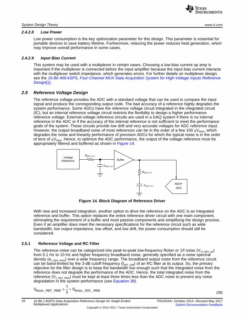
2.5 Reference Voltage DesignThe reference voltage provides the ADC with a standard voltage that can be used to compare the inputsignal and produce the corresponding output code. The bad accuracy of a reference highly degrades thesystem performance. Some ADCs have the reference voltage circuit integrated in the integrated circuit(IC), but an internal reference voltage circuit restricts the flexibility to design a higher performancereference voltage. External voltage reference circuits are used in a DAQ system if there is no internalreference in the ADC or if the accuracy of the internal reference is not sufficient to meet the performancegoals of the system. These circuits provide low drift and very accurate voltages for ADC reference input.However, the output broadband noise of most references can be in the order of a few 100 μVRMS, whichdegrades the noise and linearity performance of precision ADCs for which the typical noise is in the orderof tens of μVRMS. Hence, to optimize the ADC performance, the output of the voltage reference must beappropriately filtered and buffered as shown in Figure 14.
Figure 14. Block Diagram of Reference Driver
With new and increased integration, another option to drive the reference on the ADC is an integratedreference and buffer. This option replaces the entire reference driver circuit with one main component,eliminating the requirement of a buffer and most passive components and simplifying the design process.Even if an amplifier does meet the necessary specifications for the reference circuit such as widebandwidth, low output impedance, low offset, and low drift, the power consumption should still beconsidered.
2.5.1 Reference Voltage and RC FilterThe reference noise can be categorized into peak-to-peak low-frequency flicker or 1/f noise (V1/f_REF_pp)from 0.1 Hz to 10 Hz and higher frequency broadband noise, generally specified as a noise spectraldensity (en_REF_RMS) over a wide frequency range. The broadband output noise from the reference circuitcan be band-limited by the 3-dB cutoff frequency (fREF_3dB) of an RC filter at its output. So, the primaryobjective for the filter design is to keep the bandwidth low enough such that the integrated noise from thereference does not degrade the performance of the ADC. Hence, the total integrated noise from thereference (Vn_REF_RMS) must be kept at least three times less than the ADC noise to prevent any noisedegradation in the system performance (see Equation 38).
(38)
REF _FLTREF _3dB REF _FLT
1R
2 f C=
p ´ ´
( ) 2SNR(dB)2Q _REF 1/f _REF _PPFSR 10
REF _3dB
2 I in A VV2 1f 10
10000 nV 9 8 6.6
Hz
-é ù´ m æ öê ú£ ´ ´ ´ ´ - ç ÷
pæ ö ê úè øë ûç ÷è ø
IQ_REF (PA)
Ref
eren
ce N
oise
Den
sity
(nV
/�H
z)
1 10 100 10000
1000
2000
3000
4000
5000
6000
7000
8000
D006
Noise _REF _RMSQ _REF
1000 nV 1e
Hz 2 I (in A)» ´
´ m
2 SNR(dB)1/f _REF _PP 2 FSR 20
Noise _REF _RMS REF _3dB
V V1e f 10
6.6 2 3 2 2
-æ ö p+ ´ ´ £ ´ ´ç ÷
è ø
21/f _REF _PP 2
Noise _REF _RMS Noise _REF _RMS REF _3dB
VV e f
6.6 2
æ ö p= + ´ ´ç ÷
è ø
www.ti.com System Design Theory
19TIDU504A–October 2014–Revised May 2017Submit Documentation Feedback
Copyright © 2014–2017, Texas Instruments Incorporated
16-Bit 1-MSPS Data Acquisition Reference Design for Single-EndedMultiplexed Applications
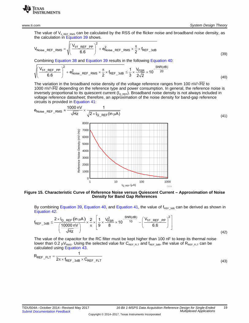
The value of Vn_REF_RMS can be calculated by the RSS of the flicker noise and broadband noise density, asthe calculation in Equation 39 shows.
(39)
Combining Equation 38 and Equation 39 results in the following Equation 40:
(40)
The variation in the broadband noise density of the voltage reference ranges from 100 nV/√Hz to1000 nV/√Hz depending on the reference type and power consumption. In general, the reference noise isinversely proportional to its quiescent current (IQ_REF). Broadband noise density is not always included involtage reference datasheet; therefore, an approximation of the noise density for band-gap referencecircuits is provided in Equation 41:
(41)
Figure 15. Characteristic Curve of Reference Noise versus Quiescent Current – Approximation of NoiseDensity for Band Gap References
By combining Equation 39, Equation 40, and Equation 41, the value of fREF_3dB can be derived as shown inEquation 42:
(42)
The value of the capacitor for the RC filter must be kept higher than 100 nF to keep its thermal noiselower than 0.2 μVRMS. Using the selected value for CREF_FLT and fREF_3dB, the value of RREF_FLT can becalculated using Equation 43.
(43)
NREF REF
BUF _FLTREF REF
Q Q 2C
V V
´= ³
D
REF REF CONV _MAXQ I T= ´
NREF REF
BUF _FLTREF REF
Q Q 2C
V V
´= ³
D
REFREF N
VV
2
D £
System Design Theory www.ti.com
20 TIDU504A–October 2014–Revised May 2017Submit Documentation Feedback
Copyright © 2014–2017, Texas Instruments Incorporated
16-Bit 1-MSPS Data Acquisition Reference Design for Single-EndedMultiplexed Applications
2.5.2 Reference Buffer and Capacitor (CBUF_FLT)Equation 44 calculates the difference in VREF between conversions:
(44)
If the charge consumed during each conversion is QREF, then the calculation is as follows in Equation 45:
(45)
The average value of QREF can be calculated from the maximum ADC conversion time (TCONV_MAX) and theaverage value of reference input current (IREF) specified in the ADC datasheets as follows in Equation 46:
(46)
By combining Equation 45 and Equation 46, the minimum value of CBUF_FLT can be obtained in thefollowing Equation 47:
(47)
The capacitor values derived from this equation are high enough to make the driving amplifier unstable, soTI recommends to use a series resistor (RBUF_FLT) to isolate the amplifier output and make it stable. Thevalue of RBUF_FLT is dependent on the output impedance of the driving amplifier as well as on the signalfrequency. Typical values of RBUF_FLT range between 0.1 Ω to 2 Ω and the exact value can be found byusing SPICE simulations. Note that higher values of RBUF_FLT cause high voltage spikes at the referencepin, which affects the conversion accuracy.
After designing the appropriate passive filter for band-limiting the noise of the reference circuit, it isimportant to select an appropriate amplifier for using as a reference buffer. The key specifications to beconsidered when selecting an appropriate amplifier for reference buffer are addressed in the followingsubsections.
2.5.3 Output ImpedanceThe output impedance for a reference buffer must be kept as low as possible because the ADC drawscurrent from the reference pin during conversion and the resultant drop in reference voltage is directlyproportional to the output impedance of the driving buffer. Maintaining this low output impedance alsohelps to keep the amplifier stable while driving a large capacitive load (CBUF_FLT).
2.5.4 Input OffsetThe input offset error of the buffer amplifier must be as low as possible to ensure that the referencevoltage driving the ADC is very accurate.
2.5.5 Offset DriftThe offset temperature drift of the reference buffer must be extremely low to ensure that the referencevoltage for the ADC does not change significantly over the operating temperature range. For similarreasons, keeping a low long-term time drift for the buffer amplifier is also important.
FLT SH
FLT
C 20 C
C 1.18 nF
³ ´
Þ ³
www.ti.com Component Selection
21TIDU504A–October 2014–Revised May 2017Submit Documentation Feedback
Copyright © 2014–2017, Texas Instruments Incorporated
16-Bit 1-MSPS Data Acquisition Reference Design for Single-EndedMultiplexed Applications
3 Component Selection
3.1 Component Selection for ADCThe ADS8860 is an excellent choice to meet the system specification for a low-power, 16-bit, 1-MSPS,single-ended DAQ application. The device operates with a 2.5-V to 5-V external reference, offering a wideselection of signal ranges without additional input signal scaling. The device supports unipolar, single-ended analog inputs in the range of –0.1 V to VREF + 0.1 V.
3.2 Component Selection for Input DriverThe input driver circuit must be able to settle within the ADC input specifications.
3.2.1 Charge Bucket Component SelectionThe charge bucket is not part of the antialiasing filter, although it is part of the analog input driver circuit.The charge bucket must be able to charge the input capacitor inside the ADC.
3.2.1.1 Reducing Charge KickbackIn Section 2.4.1, the specified value of the input capacitor for the ADS8860 is 59 pF; therefore, useEquation 48 to calculate the value of capacitance:
(48)
At first, the selected standard value of capacitance is 1.2 nF, but the final value requires confirmationusing a simulation to verify settling time and phase margin. The recommended type of capacitor is theC0G/NPO because of the low temperature coefficient and stable capacitance under varying voltages,frequency, and time.
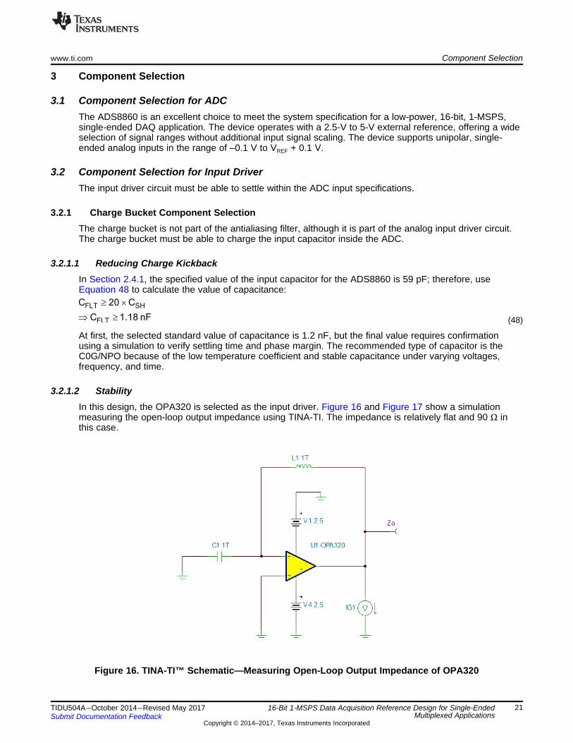
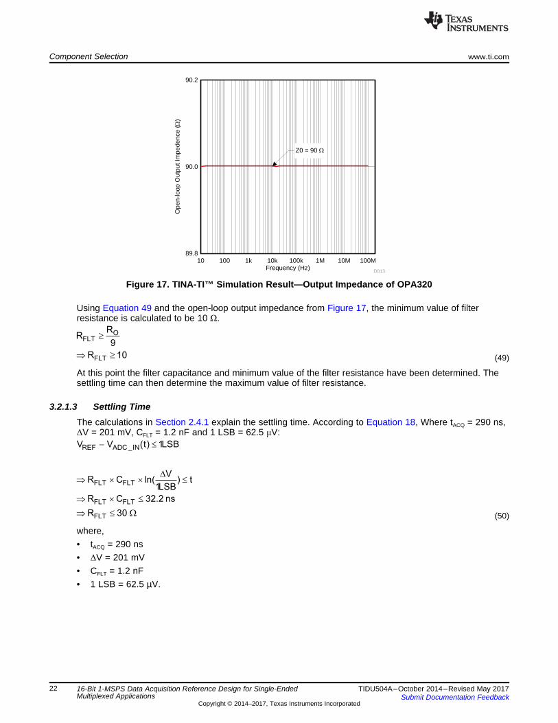
3.2.1.2 StabilityIn this design, the OPA320 is selected as the input driver. Figure 16 and Figure 17 show a simulationmeasuring the open-loop output impedance using TINA-TI. The impedance is relatively flat and 90 Ω inthis case.
Figure 16. TINA-TI™ Schematic—Measuring Open-Loop Output Impedance of OPA320
REF ADC_IN
FLT FLT
FLT FLT
FLT
V V (t) 1LSB
VR C ln( ) t
1LSB
R C 32.2 ns
R 30
- £
DÞ ´ ´ £
Þ ´ £
Þ £ W
OFLT
FLT
RR
9
R 10
³
Þ ³
Frequency (Hz)
Ope
n-lo
op O
utpu
t Im
pede
nce
(:)
89.8
90.0
90.2
10 100 1k 10k 100k 1M 10M 100M
Z0 = 90 :
D013
Component Selection www.ti.com
22 TIDU504A–October 2014–Revised May 2017Submit Documentation Feedback
Copyright © 2014–2017, Texas Instruments Incorporated
16-Bit 1-MSPS Data Acquisition Reference Design for Single-EndedMultiplexed Applications
Figure 17. TINA-TI™ Simulation Result—Output Impedance of OPA320
Using Equation 49 and the open-loop output impedance from Figure 17, the minimum value of filterresistance is calculated to be 10 Ω.
(49)
At this point the filter capacitance and minimum value of the filter resistance have been determined. Thesettling time can then determine the maximum value of filter resistance.
3.2.1.3 Settling TimeThe calculations in Section 2.4.1 explain the settling time. According to Equation 18, Where tACQ = 290 ns,ΔV = 201 mV, CFLT = 1.2 nF and 1 LSB = 62.5 μV:
(50)
where,• tACQ = 290 ns• ΔV = 201 mV• CFLT = 1.2 nF• 1 LSB = 62.5 µV.
OUT REF
QT
V VSlew Rate MAX( )
t t
6.7 VSlew Rate
s
D= =
D
Þ >m
R
R
C ADS8860
2R
C ADS8860
Differential RC Filter Common-Mode RC Filter
Copyright © 2017, Texas Instruments Incorporated
www.ti.com Component Selection
23TIDU504A–October 2014–Revised May 2017Submit Documentation Feedback
Copyright © 2014–2017, Texas Instruments Incorporated
16-Bit 1-MSPS Data Acquisition Reference Design for Single-EndedMultiplexed Applications
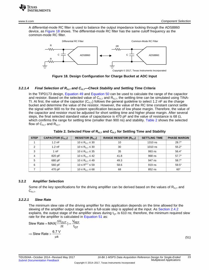
A differential-mode RC filter is used to balance the output impedance looking through the ADS8860device, as Figure 18 shows. The differential-mode RC filter has the same cutoff frequency as thecommon-mode RC filter.
Figure 18. Design Configuration for Charge Bucket at ADC Input
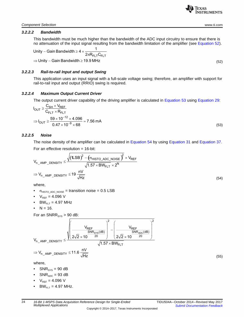
3.2.1.4 Final Selection of RFLT and CFLT—Check Stability and Settling Time CriteriaIn the TIPD173 design, Equation 49 and Equation 50 can be used to calculate the range of the capacitorand resistor. Based on the selected value of CFLT and RFLT, the settling time can be simulated using TINA-TI. At first, the value of the capacitor (CFLT) follows the general guideline to select 1.2 nF as the chargebucket and determine the value of the resistor. However, the value of the RC time constant cannot settlethe signal within 900 ns for the system specification because of low phase margin. Therefore, the value ofthe capacitor and resistor must be adjusted for short settling time and higher phase margin. After severalsteps, the final selected standard value of capacitance is 470 pF and the value of resistance is 68 Ω,which confirms the range for settling time (smaller than 900 ns) and stability. Table 2 shows the selectedflow of CFLT and RFLT.
Table 2. Selected Flow of RFLT and CFLT for Settling Time and Stability
STEP CAPACITOR (CFLT) RESISTOR (RFLT) RANGE RESISTOR (RFLT) SETTLING TIME PHASE MARGIN1 1.2 nF 10 ≤ RFLT ≤ 30 10 1310 ns 28.7°2 1.2 nF 10 ≤ RFLT ≤ 30 30 1010 ns 55.2°3 1 nF 10 ≤ RFLT ≤ 35 35 993 ns 56.4°4 820 pF 10 ≤ RFLT ≤ 42 41.8 968 ns 57.7°5 680 pF 10 ≤ RFLT ≤ 49 49.3 947 ns 58.7°6 560 pF 10 ≤ RFLT ≤ 59 58.6 919 ns 59.5°7 470 pF 10 ≤ RFLT ≤ 68 68 852 ns 60°
3.2.2 Amplifier SelectionSome of the key specifications for the driving amplifier can be derived based on the values of RFLT andCFLT.
3.2.2.1 Slew RateThe minimum slew rate of the driving amplifier for this application depends on the time allowed for theslewing of the amplifier output stage when a full-scale step is applied at the input. As Section 2.4.2explains, the output stage of the amplifier slews during tQT is 610 ns; therefore, the minimum required slewrate for the amplifier is calculated in Equation 51 as:
(51)
SYS ADC
2 2
REF REFSNR (dB) SNR (dB)
20 20
n_ AMP _DENSITYFLT
n_ AMP _DENSITY
V V
2 2 10 2 2 10V
1.57 BW
nVV 11.6
Hz
æ ö æ öç ÷ ç ÷
-ç ÷ ç ÷ç ÷ ç ÷
´ ´è ø è ø£
´
Þ £
( ) ( )22
HISTO_ADC_NOISE REF
n_ AMP _DENSITY NFLT
n_ AMP _DENSITY
1LSB VV
1.57 BW 2
nVV 19
Hz
- s ´£
´ ´
Þ £
SH REFOUT
FLT FLT
12
OUT 9
C VI
C R
59 10 4.096I 7.56 mA
0.47 10 68
-
-
´³
´
´ ´Þ ³ =
´ ´
FLT FLT
1Unity Gain Bandwidth 4
2 R C
Unity Gain Bandwidth 19.9 MHz
- ³ ´p
Þ - ³
Component Selection www.ti.com
24 TIDU504A–October 2014–Revised May 2017Submit Documentation Feedback
Copyright © 2014–2017, Texas Instruments Incorporated
16-Bit 1-MSPS Data Acquisition Reference Design for Single-EndedMultiplexed Applications
3.2.2.2 BandwidthThis bandwidth must be much higher than the bandwidth of the ADC input circuitry to ensure that there isno attenuation of the input signal resulting from the bandwidth limitation of the amplifier (see Equation 52).
(52)
3.2.2.3 Rail-to-rail Input and output SwingThis application uses an input signal with a full-scale voltage swing; therefore, an amplifier with support forrail-to-rail input and output (RRIO) swing is required.
3.2.2.4 Maximum Output Current DriverThe output current driver capability of the driving amplifier is calculated in Equation 53 using Equation 29:
(53)
3.2.2.5 NoiseThe noise density of the amplifier can be calculated in Equation 54 by using Equation 31 and Equation 37.
For an effective resolution = 16-bit:
(54)
where,• σHISTO_ADC_NOISE = transition noise = 0.5 LSB• VREF = 4.096 V• BWFLT = 4.97 MHz• N = 16.
For an SNRRSYS > 90 dB:
(55)
where,• SNRSYS = 90 dB• SNRADC = 93 dB• VREF = 4.096 V• BWFLT = 4.97 MHz.
6 9 16
BUF _FLT
300 10 710 10 2C 3.41 F
4.096
- -´ ´ ´ ´
³ = m
REF _FLT 6REF _3dB
REF _FLT 3 6
1R
2 f 10
1R 138
2 1.15 10 10
-
-
³
p ´ ´
Þ ³ = W
p ´ ´ ´
2SNR(dB)2Q _REF 1/f _REF _PPFSR 10
REF _3dB
REF _3dB
2 I (in A) VV2 1f 10
10000 nV 9 8 6.6
Hz
f 1.15 kHz
-é ù´ m æ öê ú£ ´ ´ ´ ´ - ç ÷
pæ ö ê úè øë ûç ÷è ø
Þ £
www.ti.com Component Selection
25TIDU504A–October 2014–Revised May 2017Submit Documentation Feedback
Copyright © 2014–2017, Texas Instruments Incorporated
16-Bit 1-MSPS Data Acquisition Reference Design for Single-EndedMultiplexed Applications
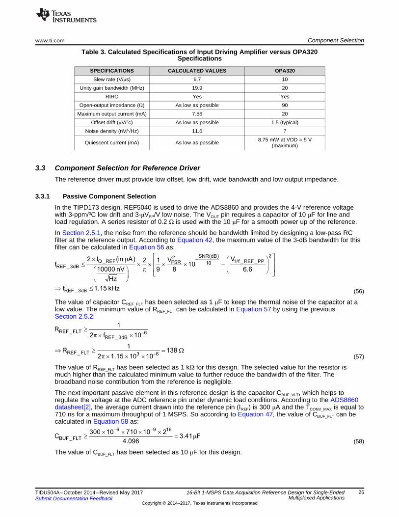
Table 3. Calculated Specifications of Input Driving Amplifier versus OPA320Specifications
SPECIFICATIONS CALCULATED VALUES OPA320Slew rate (V/μs) 6.7 10
Unity gain bandwidth (MHz) 19.9 20RIRO Yes Yes
Open-output impedance (Ω) As low as possible 90Maximum output current (mA) 7.56 20
Offset drift (μV/°c) As low as possible 1.5 (typical)Noise density (nV/√Hz) 11.6 7
Quiescent current (mA) As low as possible 8.75 mW at VDD = 5 V(maximum)
3.3 Component Selection for Reference DriverThe reference driver must provide low offset, low drift, wide bandwidth and low output impedance.
3.3.1 Passive Component SelectionIn the TIPD173 design, REF5040 is used to drive the ADS8860 and provides the 4-V reference voltagewith 3-ppm/ºC low drift and 3-μVPP/V low noise. The VOUT pin requires a capacitor of 10 μF for line andload regulation. A series resistor of 0.2 Ω is used with the 10 μF for a smooth power up of the reference.
In Section 2.5.1, the noise from the reference should be bandwidth limited by designing a low-pass RCfilter at the reference output. According to Equation 42, the maximum value of the 3-dB bandwidth for thisfilter can be calculated in Equation 56 as:
(56)
The value of capacitor CREF_FLT has been selected as 1 μF to keep the thermal noise of the capacitor at alow value. The minimum value of RREF_FLT can be calculated in Equation 57 by using the previousSection 2.5.2:
(57)
The value of RREF_FLT has been selected as 1 kΩ for this design. The selected value for the resistor ismuch higher than the calculated minimum value to further reduce the bandwidth of the filter. Thebroadband noise contribution from the reference is negligible.
The next important passive element in this reference design is the capacitor CBUF_VLT, which helps toregulate the voltage at the ADC reference pin under dynamic load conditions. According to the ADS8860datasheet[2], the average current drawn into the reference pin (IREF) is 300 μA and the TCONV_MAX is equal to710 ns for a maximum throughput of 1 MSPS. So according to Equation 47, the value of CBUF_FLT can becalculated in Equation 58 as:
(58)
The value of CBUF_FLT has been selected as 10 μF for this design.
Component Selection www.ti.com
26 TIDU504A–October 2014–Revised May 2017Submit Documentation Feedback
Copyright © 2014–2017, Texas Instruments Incorporated
16-Bit 1-MSPS Data Acquisition Reference Design for Single-EndedMultiplexed Applications
3.3.2 Integrated Reference and BufferAs previously mentioned, a new increased integration option to drive the reference on the ADC, anintegrated reference, and buffer has been added. This option replaces the entire reference driver circuitwith one main component, which avoids the long design process of choosing the correct amplifier for thebest performance. Even when an amplifier does meet the necessary specifications for a design, such aswide bandwidth, low output impedance, low offset, and low drift, the power consumption must still beconsidered as well as the design time. The REF60xx family, a high-performance line of reference driversoffered by TI, has an integrated low-output impedance buffer. Each reference driver is trimmed duringproduction to achieve a max drift of only 5 ppm/°C for both the reference and integrated buffer, combined.The device also consumes a low 820-μA quiescent current, while still being able to replenish a charge of70 pC on a 47-μF capacitor in 1 μs. This integrated device decreases design time by eliminating therequirement of the entire reference driver circuit.
The REF6041 is specifically the ideal choice for this design, with an output of 4.096 V.
3.3.3 Amplifier SelectionThe key amplifier specification to consider when designing a reference buffer for high-precision ADC arelow offset, low drift, wide bandwidth, and low output impedance. In this design, the reference buffer isdesigned using the OPA333 and THS4281 in a composite double-feedback architecture. For details ondesigning the reference driver, see the 18-Bit Data Acquisition (DAQ) Block Optimized for 1-μs Full-ScaleStep Response reference design[3].
www.ti.com Simulation
27TIDU504A–October 2014–Revised May 2017Submit Documentation Feedback
Copyright © 2014–2017, Texas Instruments Incorporated
16-Bit 1-MSPS Data Acquisition Reference Design for Single-EndedMultiplexed Applications
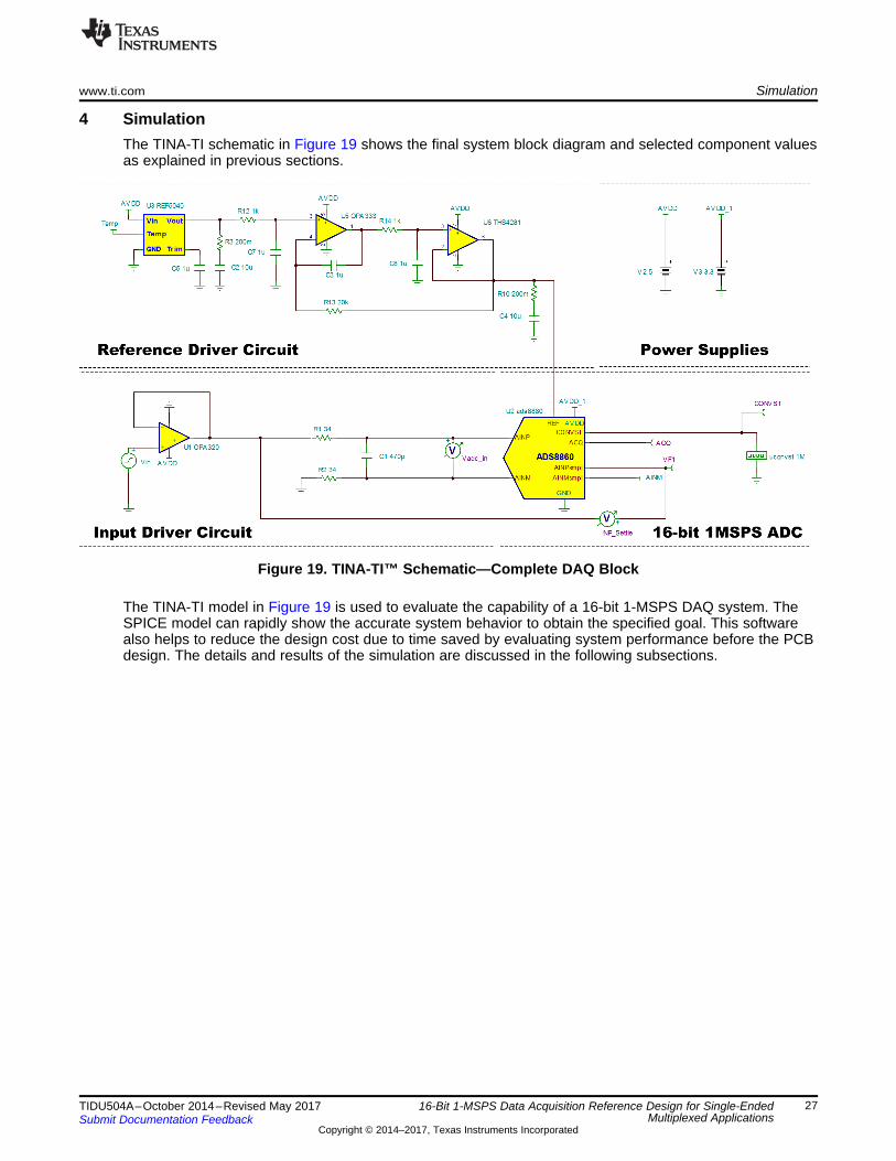
4 SimulationThe TINA-TI schematic in Figure 19 shows the final system block diagram and selected component valuesas explained in previous sections.
Figure 19. TINA-TI™ Schematic—Complete DAQ Block
The TINA-TI model in Figure 19 is used to evaluate the capability of a 16-bit 1-MSPS DAQ system. TheSPICE model can rapidly show the accurate system behavior to obtain the specified goal. This softwarealso helps to reduce the design cost due to time saved by evaluating system performance before the PCBdesign. The details and results of the simulation are discussed in the following subsections.
Simulation www.ti.com
28 TIDU504A–October 2014–Revised May 2017Submit Documentation Feedback
Copyright © 2014–2017, Texas Instruments Incorporated
16-Bit 1-MSPS Data Acquisition Reference Design for Single-EndedMultiplexed Applications
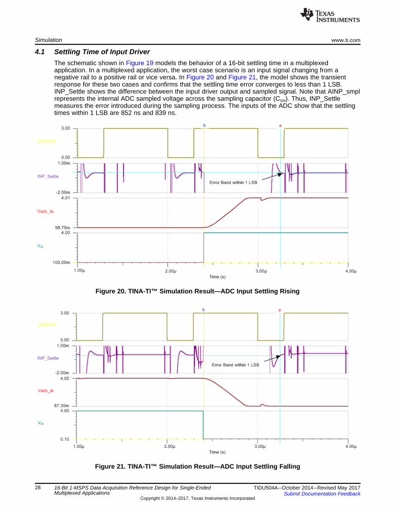
4.1 Settling Time of Input DriverThe schematic shown in Figure 19 models the behavior of a 16-bit settling time in a multiplexedapplication. In a multiplexed application, the worst case scenario is an input signal changing from anegative rail to a positive rail or vice versa. In Figure 20 and Figure 21, the model shows the transientresponse for these two cases and confirms that the settling time error converges to less than 1 LSB.INP_Settle shows the difference between the input driver output and sampled signal. Note that AINP_smplrepresents the internal ADC sampled voltage across the sampling capacitor (CSH). Thus, INP_Settlemeasures the error introduced during the sampling process. The inputs of the ADC show that the settlingtimes within 1 LSB are 852 ns and 839 ns.
Figure 20. TINA-TI™ Simulation Result—ADC Input Settling Rising
Figure 21. TINA-TI™ Simulation Result—ADC Input Settling Falling
www.ti.com Simulation
29TIDU504A–October 2014–Revised May 2017Submit Documentation Feedback
Copyright © 2014–2017, Texas Instruments Incorporated
16-Bit 1-MSPS Data Acquisition Reference Design for Single-EndedMultiplexed Applications
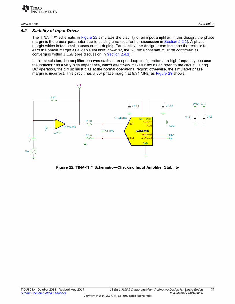
4.2 Stability of Input DriverThe TINA-TI™ schematic in Figure 22 simulates the stability of an input amplifier. In this design, the phasemargin is the crucial parameter due to settling time (see further discussion in Section 2.2.1). A phasemargin which is too small causes output ringing. For stability, the designer can increase the resistor toearn the phase margin as a viable solution; however, the RC time constant must be confirmed asconverging within 1 LSB (see discussion in Section 2.4.1).
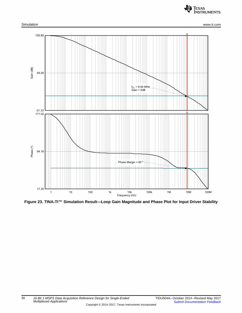
In this simulation, the amplifier behaves such as an open-loop configuration at a high frequency becausethe inductor has a very high impedance, which effectively makes it act as an open to the circuit. DuringDC operation, the circuit must bias at the normal operational region; otherwise, the simulated phasemargin is incorrect. This circuit has a 60º phase margin at 8.94 MHz, as Figure 23 shows.
Figure 22. TINA-TI™ Schematic—Checking Input Amplifier Stability
Ga
in (
dB
)
-31.33
49.28
129.89
Frequency (Hz)
Ph
ase
()º
17.35
94.18
171.02
1 10 100 1k 10k 100k 1M 10M 100M
Phase Margin = 60 º
a
b
fCL = 8.94 MHzGain = 0dB
Simulation www.ti.com
30 TIDU504A–October 2014–Revised May 2017Submit Documentation Feedback
Copyright © 2014–2017, Texas Instruments Incorporated
16-Bit 1-MSPS Data Acquisition Reference Design for Single-EndedMultiplexed Applications
Figure 23. TINA-TI™ Simulation Result—Loop Gain Magnitude and Phase Plot for Input Driver Stability
Frequency (Hz)
Tot
al n
oise
(V
)
0
9.48
18.96
1 10 100 1k 10k 100k 1M 10M 100M 1G
Total_Noise_rms = 18.97 PV
D007
www.ti.com Simulation
31TIDU504A–October 2014–Revised May 2017Submit Documentation Feedback
Copyright © 2014–2017, Texas Instruments Incorporated
16-Bit 1-MSPS Data Acquisition Reference Design for Single-EndedMultiplexed Applications
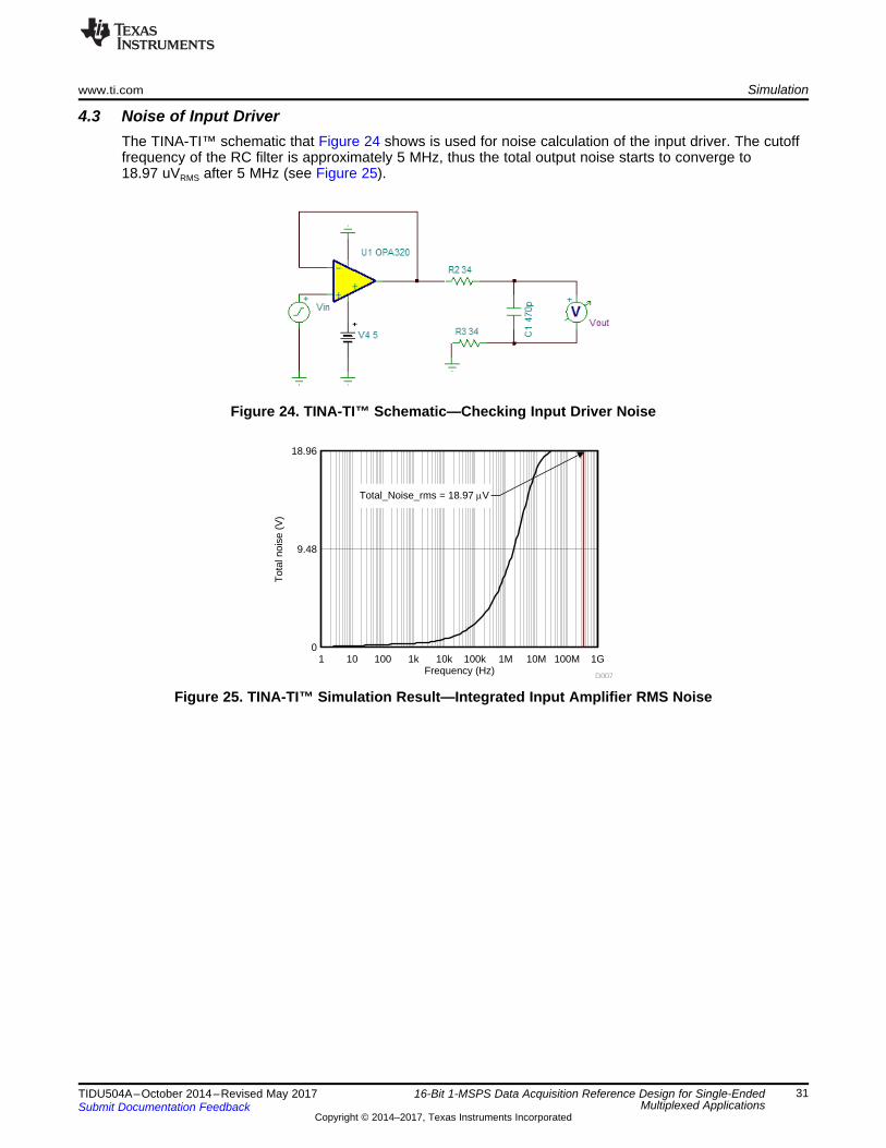
4.3 Noise of Input DriverThe TINA-TI™ schematic that Figure 24 shows is used for noise calculation of the input driver. The cutofffrequency of the RC filter is approximately 5 MHz, thus the total output noise starts to converge to18.97 uVRMS after 5 MHz (see Figure 25).
Figure 24. TINA-TI™ Schematic—Checking Input Driver Noise
Figure 25. TINA-TI™ Simulation Result—Integrated Input Amplifier RMS Noise
Time (ns)
Dig
ital C
od
e(L
SB
)
700 800 900 1000 1100 1200 13001297.0
1297.5
1298.0
1298.5
1299.0
1299.5
1300.0
1300.5
1301.0
D009
Error Band within 1LSB
Time (ns)
Dig
ita
l C
od
e(L
SB
)
700 800 900 1000 1100 1200 130065519.0
65519.5
65520.0
65520.5
65521.0
65521.5
65522.0
65522.5
65523.0
D008
Error Band within 1LSB
Verification and Measured Performance www.ti.com
32 TIDU504A–October 2014–Revised May 2017Submit Documentation Feedback
Copyright © 2014–2017, Texas Instruments Incorporated
16-Bit 1-MSPS Data Acquisition Reference Design for Single-EndedMultiplexed Applications
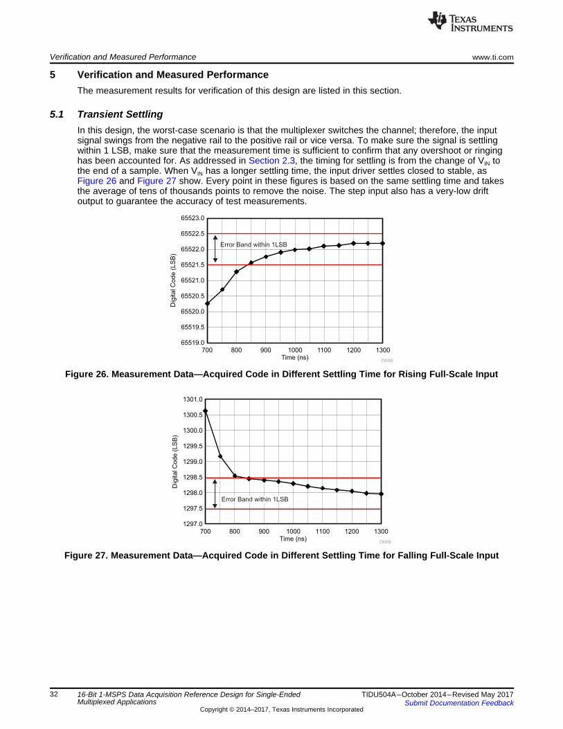
5 Verification and Measured PerformanceThe measurement results for verification of this design are listed in this section.
5.1 Transient SettlingIn this design, the worst-case scenario is that the multiplexer switches the channel; therefore, the inputsignal swings from the negative rail to the positive rail or vice versa. To make sure the signal is settlingwithin 1 LSB, make sure that the measurement time is sufficient to confirm that any overshoot or ringinghas been accounted for. As addressed in Section 2.3, the timing for settling is from the change of VIN tothe end of a sample. When VIN has a longer settling time, the input driver settles closed to stable, asFigure 26 and Figure 27 show. Every point in these figures is based on the same settling time and takesthe average of tens of thousands points to remove the noise. The step input also has a very-low driftoutput to guarantee the accuracy of test measurements.
Figure 26. Measurement Data—Acquired Code in Different Settling Time for Rising Full-Scale Input
Figure 27. Measurement Data—Acquired Code in Different Settling Time for Falling Full-Scale Input
www.ti.com Verification and Measured Performance
33TIDU504A–October 2014–Revised May 2017Submit Documentation Feedback
Copyright © 2014–2017, Texas Instruments Incorporated
16-Bit 1-MSPS Data Acquisition Reference Design for Single-EndedMultiplexed Applications
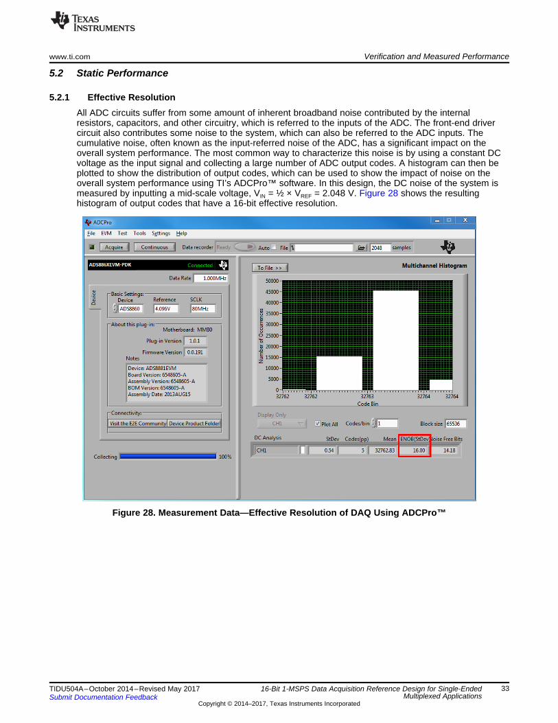
5.2 Static Performance
5.2.1 Effective ResolutionAll ADC circuits suffer from some amount of inherent broadband noise contributed by the internalresistors, capacitors, and other circuitry, which is referred to the inputs of the ADC. The front-end drivercircuit also contributes some noise to the system, which can also be referred to the ADC inputs. Thecumulative noise, often known as the input-referred noise of the ADC, has a significant impact on theoverall system performance. The most common way to characterize this noise is by using a constant DCvoltage as the input signal and collecting a large number of ADC output codes. A histogram can then beplotted to show the distribution of output codes, which can be used to show the impact of noise on theoverall system performance using TI’s ADCPro™ software. In this design, the DC noise of the system ismeasured by inputting a mid-scale voltage, VIN = ½ × VREF = 2.048 V. Figure 28 shows the resultinghistogram of output codes that have a 16-bit effective resolution.
Figure 28. Measurement Data—Effective Resolution of DAQ Using ADCPro™
Frequency (kHz)
dBc
0 20 40 60 80 100 120 140 160 180 200 220 240-180
-160
-140
-120
-100
-80
-60
-40
-20
0
HD2 (-112)
HD3 (-107)
-123
-123
-124
D011
ADC Input (V)
Non
-Lin
earit
y E
rror
(LS
B)
0.1 0.4 0.7 1 1.3 1.6 1.9 2.2 2.5 2.8 3.1 3.4 3.7 4-1
-0.5
0
0.5
1
D010
Verification and Measured Performance www.ti.com
34 TIDU504A–October 2014–Revised May 2017Submit Documentation Feedback
Copyright © 2014–2017, Texas Instruments Incorporated
16-Bit 1-MSPS Data Acquisition Reference Design for Single-EndedMultiplexed Applications
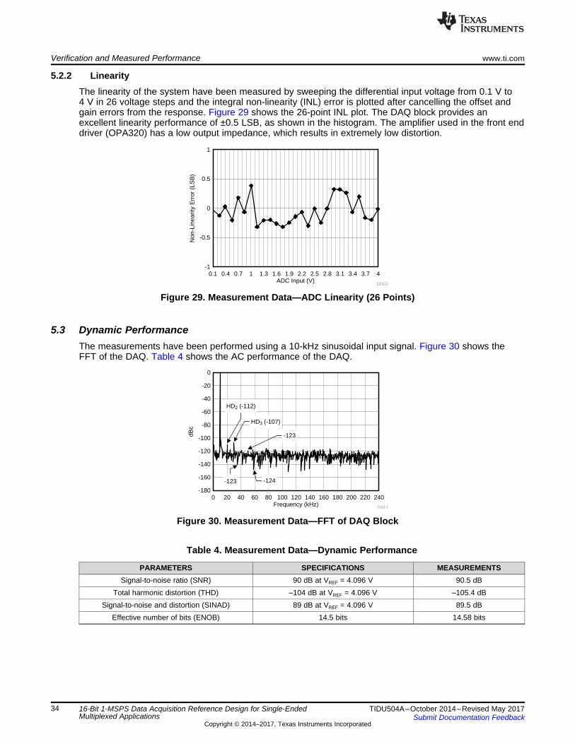
5.2.2 LinearityThe linearity of the system have been measured by sweeping the differential input voltage from 0.1 V to4 V in 26 voltage steps and the integral non-linearity (INL) error is plotted after cancelling the offset andgain errors from the response. Figure 29 shows the 26-point INL plot. The DAQ block provides anexcellent linearity performance of ±0.5 LSB, as shown in the histogram. The amplifier used in the front enddriver (OPA320) has a low output impedance, which results in extremely low distortion.
Figure 29. Measurement Data—ADC Linearity (26 Points)
5.3 Dynamic PerformanceThe measurements have been performed using a 10-kHz sinusoidal input signal. Figure 30 shows theFFT of the DAQ. Table 4 shows the AC performance of the DAQ.
Figure 30. Measurement Data—FFT of DAQ Block
Table 4. Measurement Data—Dynamic Performance
PARAMETERS SPECIFICATIONS MEASUREMENTSSignal-to-noise ratio (SNR) 90 dB at VREF = 4.096 V 90.5 dB
Total harmonic distortion (THD) –104 dB at VREF = 4.096 V –105.4 dBSignal-to-noise and distortion (SINAD) 89 dB at VREF = 4.096 V 89.5 dB
Effective number of bits (ENOB) 14.5 bits 14.58 bits
www.ti.com Modifications
35TIDU504A–October 2014–Revised May 2017Submit Documentation Feedback
Copyright © 2014–2017, Texas Instruments Incorporated
16-Bit 1-MSPS Data Acquisition Reference Design for Single-EndedMultiplexed Applications
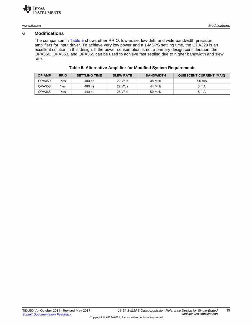
6 ModificationsThe comparison in Table 5 shows other RRIO, low-noise, low-drift, and wide-bandwidth precisionamplifiers for input driver. To achieve very low power and a 1-MSPS settling time, the OPA320 is anexcellent solution in this design. If the power consumption is not a primary design consideration, theOPA350, OPA353, and OPA365 can be used to achieve fast settling due to higher bandwidth and slewrate.
Table 5. Alternative Amplifier for Modified System Requirements
OP AMP RRIO SETTLING TIME SLEW RATE BANDWIDTH QUIESCENT CURRENT (MAX)OPA350 Yes 480 ns 22 V/μs 38 MHz 7.5 mAOPA353 Yes 480 ns 22 V/μs 44 MHz 8 mAOPA365 Yes 440 ns 25 V/μs 50 MHz 5 mA
Design Files www.ti.com
36 TIDU504A–October 2014–Revised May 2017Submit Documentation Feedback
Copyright © 2014–2017, Texas Instruments Incorporated
16-Bit 1-MSPS Data Acquisition Reference Design for Single-EndedMultiplexed Applications
7 Design Files
7.1 SchematicsTo download the schematics, see the design files at TIPD173.
7.2 Bill of MaterialsTo download the bill of materials (BOM), see the design files at TIPD173.
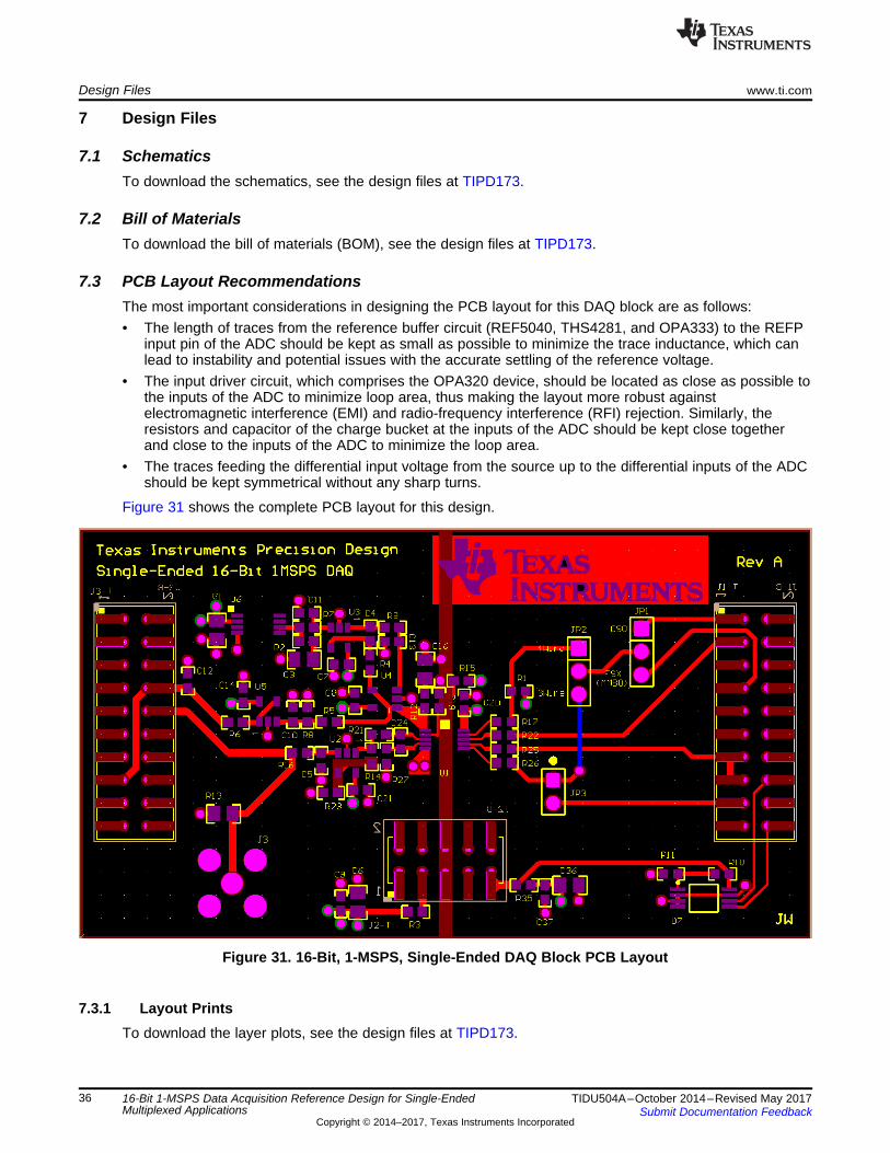
7.3 PCB Layout RecommendationsThe most important considerations in designing the PCB layout for this DAQ block are as follows:• The length of traces from the reference buffer circuit (REF5040, THS4281, and OPA333) to the REFP
input pin of the ADC should be kept as small as possible to minimize the trace inductance, which canlead to instability and potential issues with the accurate settling of the reference voltage.
• The input driver circuit, which comprises the OPA320 device, should be located as close as possible tothe inputs of the ADC to minimize loop area, thus making the layout more robust againstelectromagnetic interference (EMI) and radio-frequency interference (RFI) rejection. Similarly, theresistors and capacitor of the charge bucket at the inputs of the ADC should be kept close togetherand close to the inputs of the ADC to minimize the loop area.
• The traces feeding the differential input voltage from the source up to the differential inputs of the ADCshould be kept symmetrical without any sharp turns.
Figure 31 shows the complete PCB layout for this design.
Figure 31. 16-Bit, 1-MSPS, Single-Ended DAQ Block PCB Layout
7.3.1 Layout PrintsTo download the layer plots, see the design files at TIPD173.
www.ti.com Design Files
37TIDU504A–October 2014–Revised May 2017Submit Documentation Feedback
Copyright © 2014–2017, Texas Instruments Incorporated
16-Bit 1-MSPS Data Acquisition Reference Design for Single-EndedMultiplexed Applications
7.4 Altium ProjectTo download the Altium project files, see the design files at TIPD173.
7.5 Gerber FilesTo download the Gerber files, see the design files at TIPD173.
7.6 Assembly DrawingsTo download the assembly drawings, see the design files at TIPD173.
8 Related Documentation
1. Texas Instruments, 16-Bit, 400-kSPS, Four-Channel MUX Data Acquisition System for High-VoltageInputs Reference Design , TIPD151 Reference Design (TIDU181)
2. Texas Instruments, 16-Bit, 1-MSPS, Serial Interface, microPower, Miniature, Single-Ended Input, SARAnalog-to-Digital Converter, ADS8860 Datasheet (SBAS569)
3. Texas Instruments, 18-Bit Data Acquisition (DAQ) Block Optimized for 1-μs Full-Scale Step Response,TIPD112 Reference Design (TIDU012)
4. Kay, Art; Operational Amplifier Noise: Techniques and Tips for Analyzing and Reducing Noise,Newnes 1st Edition, 2012
5. Texas Instruments; Green, T; Selecting the right amplifier for precision CDAC SAR A/D,TI Internal Presentation, Feb 2008
6. Texas Instruments; Kay, Art; Williams, I; Slew rate, TI Precision Workshop, Unpublished7. Texas Instruments; Munikoti, Harsha; A bone of contention: ENOB or effective resolution?,
TI E2E Community Forum - Precision Hub, June 2014(http://e2e.ti.com/blogs_/b/precisionhub/archive/2014/06/13/a-bone-of-contention-enob-or-effective-resolution.aspx)
8.1 TrademarksTINA-TI, ADCPro are trademarks of Texas Instruments.All other trademarks are the property of their respective owners.
9 About the AuthorJASON WU is a field application engineer at Texas Instruments based in Taipei, Taiwan. He supports forPrecision Signal Chain product line. Jason received his MSEE from Nation Cheng Kung University inTaiwan.
Revision History A www.ti.com
38 TIDU504A–October 2014–Revised May 2017Submit Documentation Feedback
Copyright © 2014–2017, Texas Instruments Incorporated
Revision History
Revision History ANOTE: Page numbers for previous revisions may differ from page numbers in the current version.
Changes from Original (October 2014) to A Revision .................................................................................................... Page
• Added new paragraph to Reference Voltage Design ............................................................................... 18• Added Integrated Reference and Buffer subsection ................................................................................ 26• Changed schematics to updated versions available online through the Schematics subsection ............................ 36• Changed schematics to updated versions available online through the Bill of Materials subsection ........................ 36

IMPORTANT NOTICE FOR TI DESIGN INFORMATION AND RESOURCES
Texas Instruments Incorporated (‘TI”) technical, application or other design advice, services or information, including, but not limited to,reference designs and materials relating to evaluation modules, (collectively, “TI Resources”) are intended to assist designers who aredeveloping applications that incorporate TI products; by downloading, accessing or using any particular TI Resource in any way, you(individually or, if you are acting on behalf of a company, your company) agree to use it solely for this purpose and subject to the terms ofthis Notice.TI’s provision of TI Resources does not expand or otherwise alter TI’s applicable published warranties or warranty disclaimers for TIproducts, and no additional obligations or liabilities arise from TI providing such TI Resources. TI reserves the right to make corrections,enhancements, improvements and other changes to its TI Resources.You understand and agree that you remain responsible for using your independent analysis, evaluation and judgment in designing yourapplications and that you have full and exclusive responsibility to assure the safety of your applications and compliance of your applications(and of all TI products used in or for your applications) with all applicable regulations, laws and other applicable requirements. Yourepresent that, with respect to your applications, you have all the necessary expertise to create and implement safeguards that (1)anticipate dangerous consequences of failures, (2) monitor failures and their consequences, and (3) lessen the likelihood of failures thatmight cause harm and take appropriate actions. You agree that prior to using or distributing any applications that include TI products, youwill thoroughly test such applications and the functionality of such TI products as used in such applications. TI has not conducted anytesting other than that specifically described in the published documentation for a particular TI Resource.You are authorized to use, copy and modify any individual TI Resource only in connection with the development of applications that includethe TI product(s) identified in such TI Resource. NO OTHER LICENSE, EXPRESS OR IMPLIED, BY ESTOPPEL OR OTHERWISE TOANY OTHER TI INTELLECTUAL PROPERTY RIGHT, AND NO LICENSE TO ANY TECHNOLOGY OR INTELLECTUAL PROPERTYRIGHT OF TI OR ANY THIRD PARTY IS GRANTED HEREIN, including but not limited to any patent right, copyright, mask work right, orother intellectual property right relating to any combination, machine, or process in which TI products or services are used. Informationregarding or referencing third-party products or services does not constitute a license to use such products or services, or a warranty orendorsement thereof. Use of TI Resources may require a license from a third party under the patents or other intellectual property of thethird party, or a license from TI under the patents or other intellectual property of TI.TI RESOURCES ARE PROVIDED “AS IS” AND WITH ALL FAULTS. TI DISCLAIMS ALL OTHER WARRANTIES ORREPRESENTATIONS, EXPRESS OR IMPLIED, REGARDING TI RESOURCES OR USE THEREOF, INCLUDING BUT NOT LIMITED TOACCURACY OR COMPLETENESS, TITLE, ANY EPIDEMIC FAILURE WARRANTY AND ANY IMPLIED WARRANTIES OFMERCHANTABILITY, FITNESS FOR A PARTICULAR PURPOSE, AND NON-INFRINGEMENT OF ANY THIRD PARTY INTELLECTUALPROPERTY RIGHTS.TI SHALL NOT BE LIABLE FOR AND SHALL NOT DEFEND OR INDEMNIFY YOU AGAINST ANY CLAIM, INCLUDING BUT NOTLIMITED TO ANY INFRINGEMENT CLAIM THAT RELATES TO OR IS BASED ON ANY COMBINATION OF PRODUCTS EVEN IFDESCRIBED IN TI RESOURCES OR OTHERWISE. IN NO EVENT SHALL TI BE LIABLE FOR ANY ACTUAL, DIRECT, SPECIAL,COLLATERAL, INDIRECT, PUNITIVE, INCIDENTAL, CONSEQUENTIAL OR EXEMPLARY DAMAGES IN CONNECTION WITH ORARISING OUT OF TI RESOURCES OR USE THEREOF, AND REGARDLESS OF WHETHER TI HAS BEEN ADVISED OF THEPOSSIBILITY OF SUCH DAMAGES.You agree to fully indemnify TI and its representatives against any damages, costs, losses, and/or liabilities arising out of your non-compliance with the terms and provisions of this Notice.This Notice applies to TI Resources. Additional terms apply to the use and purchase of certain types of materials, TI products and services.These include; without limitation, TI’s standard terms for semiconductor products http://www.ti.com/sc/docs/stdterms.htm), evaluationmodules, and samples (http://www.ti.com/sc/docs/sampterms.htm).
Mailing Address: Texas Instruments, Post Office Box 655303, Dallas, Texas 75265Copyright © 2017, Texas Instruments Incorporated