Embed Size (px)
Citation preview
www.DataSheet4U.com
Preliminary Data
This is preliminary information on a new product now in development or undergoing evaluation. Details are subject to change without notice.
July 2007 Rev 2 1/64
1
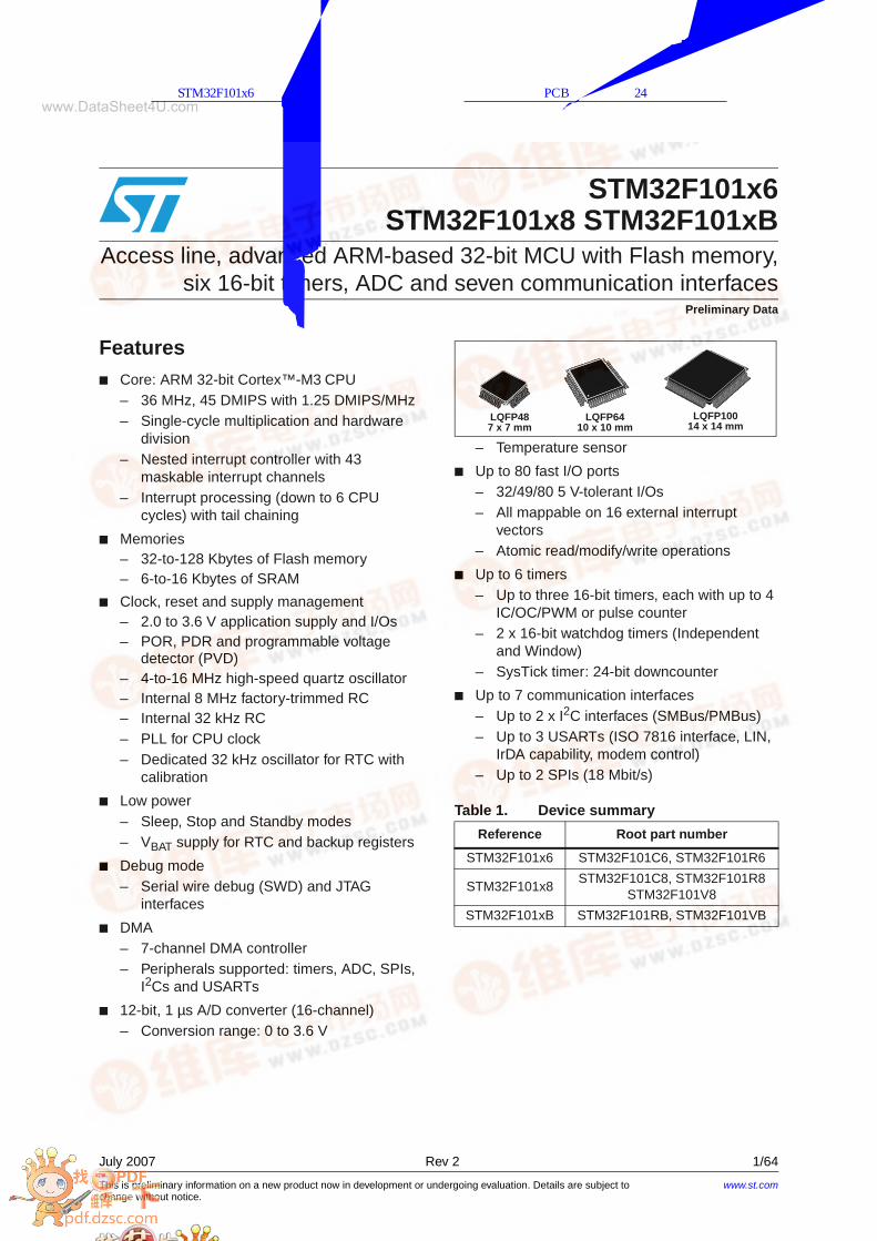
STM32F101x6STM32F101x8 STM32F101xB
Access line, advanced ARM-based 32-bit MCU with Flash memory,six 16-bit timers, ADC and seven communication interfaces
Features Core: ARM 32-bit Cortex™-M3 CPU
– 36 MHz, 45 DMIPS with 1.25 DMIPS/MHz– Single-cycle multiplication and hardware
division– Nested interrupt controller with 43
maskable interrupt channels– Interrupt processing (down to 6 CPU
cycles) with tail chaining
Memories– 32-to-128 Kbytes of Flash memory– 6-to-16 Kbytes of SRAM
Clock, reset and supply management– 2.0 to 3.6 V application supply and I/Os– POR, PDR and programmable voltage
detector (PVD)– 4-to-16 MHz high-speed quartz oscillator– Internal 8 MHz factory-trimmed RC– Internal 32 kHz RC– PLL for CPU clock– Dedicated 32 kHz oscillator for RTC with
calibration
Low power– Sleep, Stop and Standby modes– VBAT supply for RTC and backup registers
Debug mode– Serial wire debug (SWD) and JTAG
interfaces
DMA– 7-channel DMA controller– Peripherals supported: timers, ADC, SPIs,
I2Cs and USARTs
12-bit, 1 µs A/D converter (16-channel)– Conversion range: 0 to 3.6 V
– Temperature sensor
Up to 80 fast I/O ports– 32/49/80 5 V-tolerant I/Os– All mappable on 16 external interrupt
vectors– Atomic read/modify/write operations
Up to 6 timers– Up to three 16-bit timers, each with up to 4
IC/OC/PWM or pulse counter– 2 x 16-bit watchdog timers (Independent
and Window)– SysTick timer: 24-bit downcounter
Up to 7 communication interfaces– Up to 2 x I2C interfaces (SMBus/PMBus)– Up to 3 USARTs (ISO 7816 interface, LIN,
IrDA capability, modem control)– Up to 2 SPIs (18 Mbit/s)
Table 1. Device summary
Reference Root part number
STM32F101x6 STM32F101C6, STM32F101R6
STM32F101x8STM32F101C8, STM32F101R8
STM32F101V8
STM32F101xB STM32F101RB, STM32F101VB
LQFP487 x 7 mm
LQFP10014 x 14 mm
LQFP6410 x 10 mm
www.st.com
查询STM32F101x6供应商 捷多邦,专业PCB打样工厂,24小时加急出货
Contents STM32F101xx
2/64
Contents
1 Introduction . . . . . . . . . . . . . . . . . . . . . . . . . . . . . . . . . . . . . . . . . . . . . . . . 6
2 Description . . . . . . . . . . . . . . . . . . . . . . . . . . . . . . . . . . . . . . . . . . . . . . . . . 6
2.1 Device overview . . . . . . . . . . . . . . . . . . . . . . . . . . . . . . . . . . . . . . . . . . . . . 7
2.2 Overview . . . . . . . . . . . . . . . . . . . . . . . . . . . . . . . . . . . . . . . . . . . . . . . . . . 8
3 Pin descriptions . . . . . . . . . . . . . . . . . . . . . . . . . . . . . . . . . . . . . . . . . . . 14
4 Memory mapping . . . . . . . . . . . . . . . . . . . . . . . . . . . . . . . . . . . . . . . . . . 20
5 Electrical characteristics . . . . . . . . . . . . . . . . . . . . . . . . . . . . . . . . . . . . 21
5.1 Test conditions . . . . . . . . . . . . . . . . . . . . . . . . . . . . . . . . . . . . . . . . . . . . . 21
5.1.1 Minimum and maximum values . . . . . . . . . . . . . . . . . . . . . . . . . . . . . . . 21
5.1.2 Typical values . . . . . . . . . . . . . . . . . . . . . . . . . . . . . . . . . . . . . . . . . . . . . 21
5.1.3 Typical curves . . . . . . . . . . . . . . . . . . . . . . . . . . . . . . . . . . . . . . . . . . . . 21
5.1.4 Loading capacitor . . . . . . . . . . . . . . . . . . . . . . . . . . . . . . . . . . . . . . . . . 21
5.1.5 Pin input voltage . . . . . . . . . . . . . . . . . . . . . . . . . . . . . . . . . . . . . . . . . . 21
5.1.6 Power supply scheme . . . . . . . . . . . . . . . . . . . . . . . . . . . . . . . . . . . . . . 22
5.1.7 Current consumption measurement . . . . . . . . . . . . . . . . . . . . . . . . . . . 23
5.2 Absolute maximum ratings . . . . . . . . . . . . . . . . . . . . . . . . . . . . . . . . . . . . 24
5.3 Operating conditions . . . . . . . . . . . . . . . . . . . . . . . . . . . . . . . . . . . . . . . . 26
5.3.1 General operating conditions . . . . . . . . . . . . . . . . . . . . . . . . . . . . . . . . . 26
5.3.2 Operating conditions at power-up / power-down . . . . . . . . . . . . . . . . . . 26
5.3.3 Embedded reset and power control block characteristics . . . . . . . . . . . 27
5.3.4 Embedded reference voltage . . . . . . . . . . . . . . . . . . . . . . . . . . . . . . . . . 27
5.3.5 Supply current characteristics . . . . . . . . . . . . . . . . . . . . . . . . . . . . . . . . 28
5.3.6 External clock source characteristics . . . . . . . . . . . . . . . . . . . . . . . . . . . 32
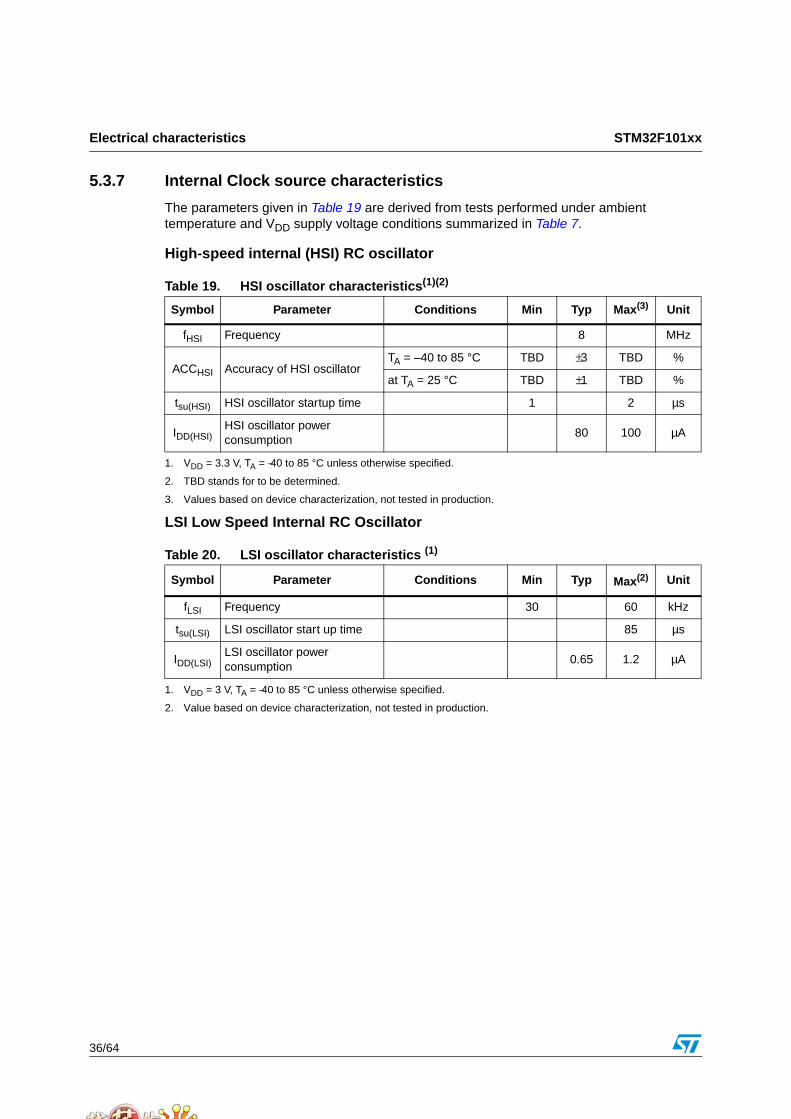
5.3.7 Internal Clock source characteristics . . . . . . . . . . . . . . . . . . . . . . . . . . . 36
5.3.8 PLL characteristics . . . . . . . . . . . . . . . . . . . . . . . . . . . . . . . . . . . . . . . . 37
5.3.9 Memory characteristics . . . . . . . . . . . . . . . . . . . . . . . . . . . . . . . . . . . . . 38
5.3.10 EMC characteristics . . . . . . . . . . . . . . . . . . . . . . . . . . . . . . . . . . . . . . . . 39
5.3.11 Absolute maximum ratings (electrical sensitivity) . . . . . . . . . . . . . . . . . 40
5.3.12 I/O port characteristics . . . . . . . . . . . . . . . . . . . . . . . . . . . . . . . . . . . . . . 42
5.3.13 NRST pin characteristics . . . . . . . . . . . . . . . . . . . . . . . . . . . . . . . . . . . . 47
STM32F101xx Contents
3/64
5.3.14 TIM timer characteristics . . . . . . . . . . . . . . . . . . . . . . . . . . . . . . . . . . . . 48
5.3.15 Communications interfaces . . . . . . . . . . . . . . . . . . . . . . . . . . . . . . . . . . 49
5.3.16 12-bit ADC characteristics . . . . . . . . . . . . . . . . . . . . . . . . . . . . . . . . . . . 54
5.3.17 Temperature sensor characteristics . . . . . . . . . . . . . . . . . . . . . . . . . . . . 57
6 Package characteristics . . . . . . . . . . . . . . . . . . . . . . . . . . . . . . . . . . . . . 58
6.1 Thermal characteristics . . . . . . . . . . . . . . . . . . . . . . . . . . . . . . . . . . . . . . 61
7 Order codes . . . . . . . . . . . . . . . . . . . . . . . . . . . . . . . . . . . . . . . . . . . . . . . 62
7.1 Future family enhancements . . . . . . . . . . . . . . . . . . . . . . . . . . . . . . . . . . 62
8 Revision history . . . . . . . . . . . . . . . . . . . . . . . . . . . . . . . . . . . . . . . . . . . 63
List of tables STM32F101xx
4/64
List of tables
Table 1. Device summary . . . . . . . . . . . . . . . . . . . . . . . . . . . . . . . . . . . . . . . . . . . . . . . . . . . . . . . . . . 1Table 2. Device features and peripheral counts (STM32F101xx access line) . . . . . . . . . . . . . . . . . . 7Table 3. Pin definitions . . . . . . . . . . . . . . . . . . . . . . . . . . . . . . . . . . . . . . . . . . . . . . . . . . . . . . . . . . . 16Table 4. Voltage characteristics . . . . . . . . . . . . . . . . . . . . . . . . . . . . . . . . . . . . . . . . . . . . . . . . . . . . 24Table 5. Current characteristics . . . . . . . . . . . . . . . . . . . . . . . . . . . . . . . . . . . . . . . . . . . . . . . . . . . . 24Table 6. Thermal characteristics. . . . . . . . . . . . . . . . . . . . . . . . . . . . . . . . . . . . . . . . . . . . . . . . . . . . 25Table 7. General operating conditions . . . . . . . . . . . . . . . . . . . . . . . . . . . . . . . . . . . . . . . . . . . . . . . 26Table 8. Operating conditions at power-up / power-down . . . . . . . . . . . . . . . . . . . . . . . . . . . . . . . . 26Table 9. Embedded reset and power control block characteristics. . . . . . . . . . . . . . . . . . . . . . . . . . 27Table 10. Embedded internal reference voltage. . . . . . . . . . . . . . . . . . . . . . . . . . . . . . . . . . . . . . . . . 27Table 11. Maximum current consumption in Run and Sleep modes (TA = 85 °C) . . . . . . . . . . . . . . . 28Table 12. Maximum current consumption in Stop and Standby modes . . . . . . . . . . . . . . . . . . . . . . . 29Table 13. Typical current consumption in Run and Sleep modes . . . . . . . . . . . . . . . . . . . . . . . . . . . 30Table 14. Typical current consumption in Stop and Standby modes . . . . . . . . . . . . . . . . . . . . . . . . . 31Table 15. High-speed user external (HSE) clock characteristics . . . . . . . . . . . . . . . . . . . . . . . . . . . . 32Table 16. Low-speed user external clock characteristics . . . . . . . . . . . . . . . . . . . . . . . . . . . . . . . . . . 32Table 17. HSE 4-16 MHz oscillator characteristics. . . . . . . . . . . . . . . . . . . . . . . . . . . . . . . . . . . . . . . 34Table 18. LSE oscillator characteristics (fLSE = 32.768 kHz) . . . . . . . . . . . . . . . . . . . . . . . . . . . . . . . 35Table 19. HSI oscillator characteristics. . . . . . . . . . . . . . . . . . . . . . . . . . . . . . . . . . . . . . . . . . . . . . . . 36Table 20. LSI oscillator characteristics . . . . . . . . . . . . . . . . . . . . . . . . . . . . . . . . . . . . . . . . . . . . . . . 36Table 21. Low-power mode wakeup timings . . . . . . . . . . . . . . . . . . . . . . . . . . . . . . . . . . . . . . . . . . . 37Table 22. PLL characteristics . . . . . . . . . . . . . . . . . . . . . . . . . . . . . . . . . . . . . . . . . . . . . . . . . . . . . . . 37Table 23. Flash memory characteristics . . . . . . . . . . . . . . . . . . . . . . . . . . . . . . . . . . . . . . . . . . . . . . . 38Table 24. Flash endurance and data retention . . . . . . . . . . . . . . . . . . . . . . . . . . . . . . . . . . . . . . . . . . 38Table 25. EMS characteristics . . . . . . . . . . . . . . . . . . . . . . . . . . . . . . . . . . . . . . . . . . . . . . . . . . . . . . 39Table 26. EMI characteristics . . . . . . . . . . . . . . . . . . . . . . . . . . . . . . . . . . . . . . . . . . . . . . . . . . . . . . . 40Table 27. ESD absolute maximum ratings . . . . . . . . . . . . . . . . . . . . . . . . . . . . . . . . . . . . . . . . . . . . . 40Table 28. Electrical sensitivities . . . . . . . . . . . . . . . . . . . . . . . . . . . . . . . . . . . . . . . . . . . . . . . . . . . . . 41Table 29. I/O static characteristics . . . . . . . . . . . . . . . . . . . . . . . . . . . . . . . . . . . . . . . . . . . . . . . . . . . 42Table 30. Output voltage characteristics . . . . . . . . . . . . . . . . . . . . . . . . . . . . . . . . . . . . . . . . . . . . . . 44Table 31. I/O AC characteristics . . . . . . . . . . . . . . . . . . . . . . . . . . . . . . . . . . . . . . . . . . . . . . . . . . . . . 45Table 32. NRST pin characteristics . . . . . . . . . . . . . . . . . . . . . . . . . . . . . . . . . . . . . . . . . . . . . . . . . . 47Table 33. TIMx characteristics . . . . . . . . . . . . . . . . . . . . . . . . . . . . . . . . . . . . . . . . . . . . . . . . . . . . . . 48Table 34. I2C characteristics. . . . . . . . . . . . . . . . . . . . . . . . . . . . . . . . . . . . . . . . . . . . . . . . . . . . . . . . 49Table 35. SCL frequency (fPCLK1= 36 MHz, VDD = 3.3 V) . . . . . . . . . . . . . . . . . . . . . . . . . . . . . . . . . 50Table 36. SPI characteristics . . . . . . . . . . . . . . . . . . . . . . . . . . . . . . . . . . . . . . . . . . . . . . . . . . . . . . . 51Table 37. ADC characteristics . . . . . . . . . . . . . . . . . . . . . . . . . . . . . . . . . . . . . . . . . . . . . . . . . . . . . . 54Table 38. ADC accuracy (fPCLK2 = 10 MHz, fADC = 10 MHz, RAIN < 10 kΩ, VDDA = 3.3 V) . . . . . . . . 55Table 39. TS characteristics . . . . . . . . . . . . . . . . . . . . . . . . . . . . . . . . . . . . . . . . . . . . . . . . . . . . . . . . 57Table 40. LQPF100 – 100-pin low-profile quad flat package mechanical data . . . . . . . . . . . . . . . . . 58Table 41. LQFP64 – 64-pin low-profile quad flat package mechanical data . . . . . . . . . . . . . . . . . . . 59Table 42. LQFP48 – 48-pin low-profile quad flat package mechanical data . . . . . . . . . . . . . . . . . . . 60Table 43. Thermal characteristics. . . . . . . . . . . . . . . . . . . . . . . . . . . . . . . . . . . . . . . . . . . . . . . . . . . . 61Table 44. Order codes . . . . . . . . . . . . . . . . . . . . . . . . . . . . . . . . . . . . . . . . . . . . . . . . . . . . . . . . . . . . 62Table 45. Document revision history . . . . . . . . . . . . . . . . . . . . . . . . . . . . . . . . . . . . . . . . . . . . . . . . . 63
STM32F101xx List of figures
5/64
List of figures
Figure 1. STM32F101xx access line block diagram . . . . . . . . . . . . . . . . . . . . . . . . . . . . . . . . . . . 13Figure 2. STM32F101xx access line LQFP100 pinout . . . . . . . . . . . . . . . . . . . . . . . . . . . . . . . . . . . 14Figure 3. STM32F101xx access line LQFP64 pinout . . . . . . . . . . . . . . . . . . . . . . . . . . . . . . . . . . . . 15Figure 4. STM32F101xx access line LQFP48 pinout . . . . . . . . . . . . . . . . . . . . . . . . . . . . . . . . . . . . 15Figure 5. Memory map. . . . . . . . . . . . . . . . . . . . . . . . . . . . . . . . . . . . . . . . . . . . . . . . . . . . . . . . . . . . 20Figure 6. Pin loading conditions. . . . . . . . . . . . . . . . . . . . . . . . . . . . . . . . . . . . . . . . . . . . . . . . . . . . . 22Figure 7. Pin input voltage . . . . . . . . . . . . . . . . . . . . . . . . . . . . . . . . . . . . . . . . . . . . . . . . . . . . . . . . . 22Figure 8. Power supply scheme. . . . . . . . . . . . . . . . . . . . . . . . . . . . . . . . . . . . . . . . . . . . . . . . . . . . . 22Figure 9. Current consumption measurement scheme . . . . . . . . . . . . . . . . . . . . . . . . . . . . . . . . . . . 23Figure 10. High-speed external clock source AC timing diagram . . . . . . . . . . . . . . . . . . . . . . . . . . . . 33Figure 11. Low-speed external clock source AC timing diagram. . . . . . . . . . . . . . . . . . . . . . . . . . . . . 33Figure 12. Typical application with an 8 MHz crystal . . . . . . . . . . . . . . . . . . . . . . . . . . . . . . . . . . . . . . 34Figure 13. Typical application with a 32.768 kHz crystal . . . . . . . . . . . . . . . . . . . . . . . . . . . . . . . . . . . 35Figure 14. Unused I/O pin connection . . . . . . . . . . . . . . . . . . . . . . . . . . . . . . . . . . . . . . . . . . . . . . . . . 43Figure 15. I/O AC characteristics definition . . . . . . . . . . . . . . . . . . . . . . . . . . . . . . . . . . . . . . . . . . . . . 46Figure 16. Recommended NRST pin protection . . . . . . . . . . . . . . . . . . . . . . . . . . . . . . . . . . . . . . . . . 47Figure 17. I2C bus AC waveforms and measurement circuit . . . . . . . . . . . . . . . . . . . . . . . . . . . . . . . 50Figure 18. SPI timing diagram - slave mode and CPHA=0 . . . . . . . . . . . . . . . . . . . . . . . . . . . . . . . . . 52Figure 19. SPI timing diagram - slave mode and CPHA=11). . . . . . . . . . . . . . . . . . . . . . . . . . . . . . . . 52Figure 20. SPI timing diagram - master mode . . . . . . . . . . . . . . . . . . . . . . . . . . . . . . . . . . . . . . . . . . . 53Figure 21. ADC accuracy characteristics. . . . . . . . . . . . . . . . . . . . . . . . . . . . . . . . . . . . . . . . . . . . . . . 55Figure 22. Typical connection diagram using the ADC . . . . . . . . . . . . . . . . . . . . . . . . . . . . . . . . . . . . 55Figure 23. Power supply and reference decoupling (VREF+ not connected to VDDA). . . . . . . . . . . . . . 56Figure 24. Power supply and reference decoupling (VREF+ connected to VDDA) . . . . . . . . . . . . . . . 56Figure 25. LQPF100 – 100-pin low-profile quad flat package outline . . . . . . . . . . . . . . . . . . . . . . . . . 58Figure 26. LQFP64 – 64-pin low-profile quad flat package outline . . . . . . . . . . . . . . . . . . . . . . . . . . . 59Figure 27. LQFP48 – 48-pin low-profile quad flat package outline . . . . . . . . . . . . . . . . . . . . . . . . . . . 60
Introduction STM32F101xx
6/64
1 Introduction
This datasheet contains the description of the STM32F101xx access line family features, pinout, Electrical Characteristics, Mechanical Data and Ordering information.
For information on programming, erasing and protection of the internal Flash memory please refer to the STM32F10x Flash Programming Reference Manual
For information on the Cortex™-M3 core please refer to the Cortex™-M3 Technical Reference Manual.
2 Description
The STM32F101xx access line family incorporates the high-performance ARM Cortex™-M3 32-bit RISC core operating at a 36 MHz frequency, high-speed embedded memories (Flash memory up to 128Kbytes and SRAM up to 16 Kbytes), and an extensive range of enhanced peripherals and I/Os connected to two APB buses. All devices offer standard communication interfaces (two I2Cs, two SPIs, and up to three USARTs), one 12-bit ADC and three general purpose 16-bit timers.
The STM32F101 family operates in the −40 to +85°C temperature range, from a 2.0 to 3.6 V power supply. A comprehensive set of power-saving mode allows to design low-power applications.
The complete STM32F101xx access line family includes devices in 3 different package types: from 48 pins to 100 pins. Depending on the device chosen, different sets of peripherals are included, the description below gives an overview of the complete range of peripherals proposed in this family.
These features make the STM32F101xx access line microcontroller family suitable for a wide range of applications:
Application control and user interface
Medical and handheld equipment
PC peripherals, gaming and GPS platforms
Industrial applications: PLC, inverters, printers, and scanners
Alarm systems, Video intercom, and HVAC
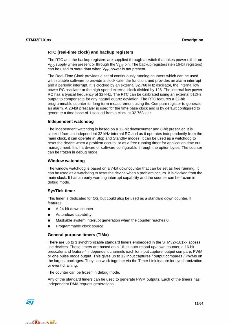
Figure 1 shows the general block diagram of the device family.
STM32F101xx Description
7/64
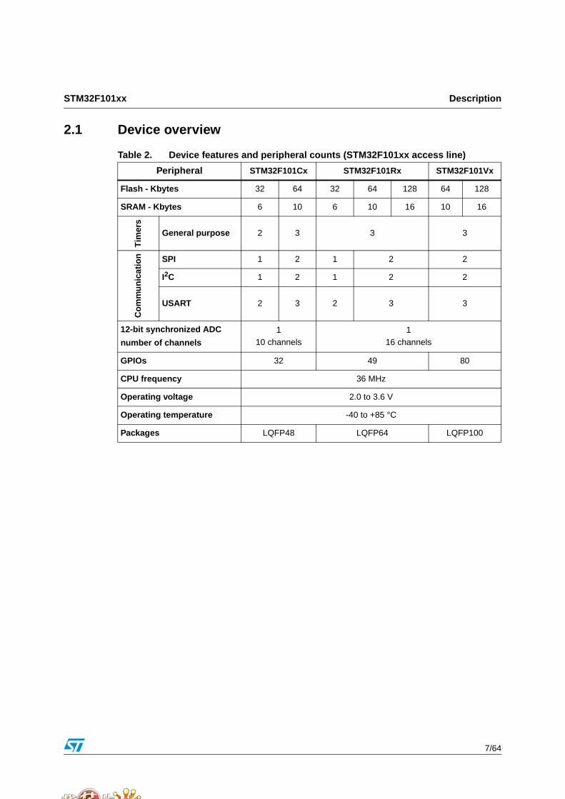
2.1 Device overview
Table 2. Device features and peripheral counts (STM32F101xx access line)
Peripheral STM32F101Cx STM32F101Rx STM32F101Vx
Flash - Kbytes 32 64 32 64 128 64 128
SRAM - Kbytes 6 10 6 10 16 10 16
Tim
ers
General purpose 2 3 3 3
Co
mm
un
icat
ion SPI 1 2 1 2 2
I2C 1 2 1 2 2
USART 2 3 2 3 3
12-bit synchronized ADC
number of channels
110 channels
116 channels
GPIOs 32 49 80
CPU frequency 36 MHz
Operating voltage 2.0 to 3.6 V
Operating temperature -40 to +85 °C
Packages LQFP48 LQFP64 LQFP100

Description STM32F101xx
8/64
2.2 Overview
ARM® CortexTM-M3 core with embedded Flash and SRAM
The ARM Cortex™-M3 processor is the latest generation of ARM processors for embedded systems. It has been developed to provide a low-cost platform that meets the needs of MCU implementation, with a reduced pin count and low-power consumption, while delivering outstanding computational performance and an advanced system response to interrupts.
The ARM Cortex™-M3 32-bit RISC processor features exceptional code-efficiency, delivering the high-performance expected from an ARM core in the memory size usually associated with 8- and 16-bit devices.
The STM32F101xx access line family having an embedded ARM core, is therefore compatible with all ARM tools and software.
Embedded Flash memory
Up to 128 Kbytes of embedded Flash is available for storing programs and data.
Embedded SRAM
Up to 16 Kbytes of embedded SRAM accessed (read/write) at CPU clock speed with 0 wait states.
Nested vectored interrupt controller (NVIC)
The STM32F101xx access line embeds a nested vectored interrupt controller able to handle up to 43 maskable interrupt channels (not including the 16 interrupt lines of Cortex™-M3) and 16 priority levels.
Closely coupled NVIC gives low latency interrupt processing
Interrupt entry vector table address passed directly to the core
Closely coupled NVIC core interface
Allows early processing of interrupts
Processing of late arriving higher priority interrupts
Support for tail-chaining
Processor state automatically saved
Interrupt entry restored on interrupt exit with no instruction overhead
This hardware block provides flexible interrupt management features with minimal interrupt latency.
STM32F101xx Description
9/64
External interrupt/event controller (EXTI)
The external interrupt/event controller consists of 19 edge detectors lines used to generate interrupt/event requests. Each line can be independently configured to select the trigger event (rising edge, falling edge, both) and can be masked independently. A pending register maintains the status of the interrupt requests. The EXTI can detect external line with pulse width lower than the Internal APB2 clock period. Up to 80 GPIOs are connected to the 16 external interrupt lines.
Clocks and startup
System clock selection is performed on startup, however the internal RC 8 MHz oscillator is selected as default CPU clock on reset. An external 4-16 MHz clock can be selected and is monitored for failure. During such a scenario, it is disabled and software interrupt management follows. Similarly, full interrupt management of the PLL clock entry is available when necessary (for example with failure of an indirectly used external oscillator).
Several prescalers allow the configuration of the AHB frequency, the High Speed APB (APB2) and the low Speed APB (APB1) domains. The maximum frequency of the AHB and the APB domains is 36 MHz.
Boot modes
At startup, boot pins are used to select one of five boot options:
Boot from User Flash
Boot from System Memory
Boot from SRAM
The boot loader is located in System Memory. It is used to reprogram the Flash memory by using the USART.
Power supply schemes
VDD = 2.0 to 3.6 V: External power supply for I/Os and the internal regulator. Provided externally through VDD pins.
VSSA, VDDA = 2.0 to 3.6 V: External analog power supplies for ADC, Reset blocks, RCs and PLL. In VDD range (ADC is limited at 2.4 V).
VBAT = 1.8 to 3.6 V: Power supply for RTC, external clock 32 kHz oscillator and backup registers (through power switch) when VDD is not present.
Power supply supervisor
The device has an integrated power on reset (POR)/power down reset (PDR) circuitry. It is always active, and ensures proper operation starting from/down to 2 V. The device remains in reset mode when VDD is below a specified threshold, VPOR/PDR, without the need for an external reset circuit.
The device features an embedded Programmable voltage detector (PVD) that monitors the VDD power supply and compares it to the VPVD threshold. An interrupt can be generated when VDD drops below the VPVD and/or when VDD is higher than the VPVD threshold. The interrupt service routine can then generate a warning message and/or put the MCU into a safe state. The PVD is enabled by software.
Refer to Table 9: Embedded reset and power control block characteristics for the values of VPOR/PDR and VPVD.
Description STM32F101xx
10/64
Voltage regulator
The regulator has three operation modes: main (MR), low power (LPR) and power down.
MR is used in the nominal regulation mode (Run)
LPR is used in the Stop modes
Power down is used in Standby Mode: the regulator output is in high impedance: the kernel circuitry is powered-down, inducing zero consumption (but the contents of the registers and SRAM are lost)
This regulator is always enabled after RESET. It is disabled in Standby Mode, providing high impedance output.
Low-power modes
The STM32F101xx access line supports three low-power modes to achieve the best compromise between low power consumption, short startup time and available wakeup sources:
Sleep mode
In Sleep mode, only the CPU is stopped. All peripherals continue to operate and can wake up the CPU when an interrupt/event occurs.
Stop mode
Stop mode allows to achieve the lowest power consumption while retaining the content of SRAM and registers. All clocks in the 1.8 V domain are stopped, the PLL, the HSI and the HSE RC oscillators are disabled. The voltage regulator can also be put either in normal or in low power mode. The device can be woken up from Stop mode by any of the EXTI line. The EXTI line source can be one of the 16 external lines, the PVD output or the RTC alarm.
Standby mode
The Standby mode allows to achieve the lowest power consumption. The internal voltage regulator is switched off so that the entire 1.8 V domain is powered off. The PLL, the HSI and the HSE RC oscillators are also switched off. After entering Standby mode, SRAM and registers content are lost except for registers in the Backup domain and Standby circuitry.
The device exits Standby mode when an external reset (NRST pin), a IWDG reset, a rising edge on the WKUP pin, or an RTC alarm occurs.
Note: The RTC, the IWDG, and the corresponding clock sources are not stopped by entering Stop or Standby mode.
DMA
The flexible 7-channel general-purpose DMA is able to manage memory-to-memory, peripheral-to-memory and memory-to-peripheral transfers. The DMA controller supports circular buffer management avoiding the generation of interrupts when the controller reaches the end of the buffer.
Each channel is connected to dedicated hardware DMA requests, with support for software trigger on each channel. Configuration is made by software and transfer sizes between source and destination are independent.
The DMA can be used with the main peripherals: SPI, I2C, USART, general purpose timers TIMx and ADC.
STM32F101xx Description
11/64
RTC (real-time clock) and backup registers
The RTC and the backup registers are supplied through a switch that takes power either on VDD supply when present or through the VBAT pin. The backup registers (ten 16-bit registers) can be used to store data when VDD power is not present.
The Real-Time Clock provides a set of continuously running counters which can be used with suitable software to provide a clock calendar function, and provides an alarm interrupt and a periodic interrupt. It is clocked by an external 32.768 kHz oscillator, the internal low power RC oscillator or the high-speed external clock divided by 128. The internal low power RC has a typical frequency of 32 kHz. The RTC can be calibrated using an external 512Hz output to compensate for any natural quartz deviation. The RTC features a 32-bit programmable counter for long term measurement using the Compare register to generate an alarm. A 20-bit prescaler is used for the time base clock and is by default configured to generate a time base of 1 second from a clock at 32.768 kHz.
Independent watchdog
The independent watchdog is based on a 12-bit downcounter and 8-bit prescaler. It is clocked from an independent 32 kHz internal RC and as it operates independently from the main clock, it can operate in Stop and Standby modes. It can be used as a watchdog to reset the device when a problem occurs, or as a free running timer for application time out management. It is hardware or software configurable through the option bytes. The counter can be frozen in debug mode.
Window watchdog
The window watchdog is based on a 7-bit downcounter that can be set as free running. It can be used as a watchdog to reset the device when a problem occurs. It is clocked from the main clock. It has an early warning interrupt capability and the counter can be frozen in debug mode.
SysTick timer
This timer is dedicated for OS, but could also be used as a standard down counter. It features:
A 24-bit down counter
Autoreload capability
Maskable system interrupt generation when the counter reaches 0.
Programmable clock source
General purpose timers (TIMx)
There are up to 3 synchronizable standard timers embedded in the STM32F101xx access line devices. These timers are based on a 16-bit auto-reload up/down counter, a 16-bit prescaler and feature 4 independent channels each for input capture, output compare, PWM or one pulse mode output. This gives up to 12 input captures / output compares / PWMs on the largest packages. They can work together via the Timer Link feature for synchronization or event chaining.
The counter can be frozen in debug mode.
Any of the standard timers can be used to generate PWM outputs. Each of the timers has independent DMA request generations.
Description STM32F101xx
12/64
I²C bus
Up to two I²C bus interfaces can operate in multi-master and slave modes. They can support standard and fast modes.
They support dual slave addressing (7-bit only) and both 7/10-bit addressing in master mode. A hardware CRC generation/verification is embedded.
They can be served by DMA and they support SM Bus 2.0/PM Bus.
Universal synchronous/asynchronous receiver transmitter (USART)
The available USART interfaces communicate at up to 2.25 Mbit/s. They provide hardware management of the CTS and RTS signals, support IrDA SIR ENDEC, are ISO 7816 compliant and have LIN Master/Slave capability.
The USART interfaces can be served by the DMA controller.
Serial peripheral interface (SPI)
Up to two SPIs are able to communicate up to 18 Mbits/s in slave and master modes in full-duplex and simplex communication modes. The 3-bit prescaler gives 8 master mode frequencies and the frame is configurable from 8-bit to 16-bit. The hardware CRC generation/verification supports basic SD Card/MMC modes.
Both SPIs can be served by the DMA controller.
GPIOs (general purpose inputs/outputs)
Each of the GPIO pins can be configured by software as output (push-pull or open-drain), as input (with or without pull-up or pull-down) or as Peripheral Alternate Function. Most of the GPIO pins are shared with digital or analog alternate functions. All GPIOs are high current-capable.
The I/Os alternate function configuration can be locked if needed following a specific sequence in order to avoid spurious writing to the I/Os registers.
ADC (analog to digital converter)
The 12-bit Analog to Digital Converter has up to 16 external channels and performs conversions in single-shot or scan modes. In scan mode, automatic conversion is performed on a selected group of analog inputs.
The ADC can be served by the DMA controller.
An analog watchdog feature allows very precise monitoring of the converted voltage of one, some or all selected channels. An interrupt is generated when the converted voltage is outside the programmed thresholds.
Temperature sensor
The temperature sensor has to generate a linear voltage with any variation in temperature. The conversion range is between 2V < VDDA < 3.6V. The temperature sensor is internally connected to the ADC_IN16 input channel which is used to convert the sensor output voltage into a digital value.
STM32F101xx Description
13/64
Serial wire JTAG debug port (SWJ-DP)
The ARM SWJ-DP Interface is embedded. and is a combined JTAG and serial wire debug port that enables either a serial wire debug or a JTAG probe to be connected to the target. The JTAG TMS and TCK pins are shared respectively with SWDIO and SWCLK and a specific sequence on the TMS pin is used to switch between JTAG-DP and SW-DP.
Figure 1. STM32F101xx access line block diagram
1. AF = alternate function on I/O port pin.
2. TA = –40 °C to +85 °C (junction temperature up to 125 °C).
Temp sensor
PA[15:0]
EXTI
W W D G
NVIC
12bit ADC1
JTAG & SWD
16AF
JTDIJTCK/SWCLKJTMS/SWDIO
JNTRST
JTDO
NRST
VDD = 2 to 3.6V
80AF
PB[15:0]
PC[15:0]
AHB2
MOSI,MISO,SCK,NSS
SRAM
2x(8x16bit)
WAKEUP
GPIOA
GPIOB
GPIOC
Fmax: 36 MHz
VSS
SCL,SDAI2C2
VREF+
GP DMA
TIM2
TIM3
XTAL OSC 4-16 MHz
XTAL 32 kHz
OSC_INOSC_OUT
OSC32_OUTOSC32_IN
PLL &
APB
1 : F
max
=24
/ 36
MH
z
PCLK1
HCLKCLOCK MANAGT
PCLK2
as AF
as AF
VOLT. REG.3.3V TO 1.8V
POWER
Backup interface
as AF
16 KB
RTC
RC 8 MHz
Cortex M3 CPU
USART1
USART2
SPI2
7 channels
Backupreg
SCL,SDA,SMBALI2C1as AF
RX,TX, CTS, RTS,USART3
VREF-
PD[15:0] GPIOD
AH
B:F
max
=36
MH
z
4 Channels
4 Channels
FCLK
RC 32 kHzStandby
IWDG
@VDD
@VBATPOR / PDR
SUPPLY
@VDDA
VDDAVSSA
@VDDA
VBAT
SmartCard as AF
RX,TX, CTS, RTS,SmartCard as AF
RX,TX, CTS, RTS,SmartCard as AF
APB
2 : F
max
= 36
MH
z
NVIC
SPI1MOSI,MISO,SCK,NSS as AF
IF
interface@VDDA
SUPERVISION
PVD
Rst
Int
@VDD
AHB2APB2 APB1 AWU ANTI_TAMP
PE[15:0] GPIOE
FLASH 128 KB
BusM
atrix
64 bit
Inte
rfac
eIbus
Dbus
pbus
obl
Flas
h
Trace Controller
System
TIM4 4 Channels
ai14385
Pin descriptions STM32F101xx
14/64
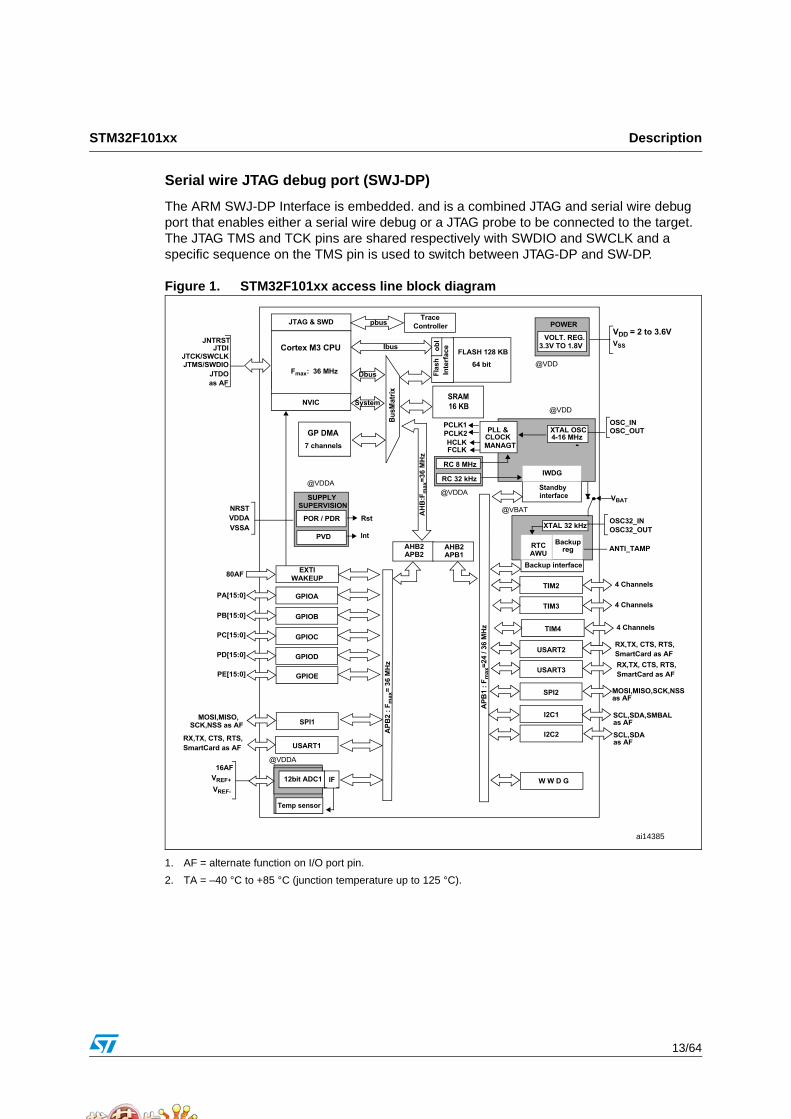
3 Pin descriptions
Figure 2. STM32F101xx access line LQFP100 pinout
100
99 98 97 96 95 94 93 92 91 90 89 88 87 86 85 84 83 82 81 80 79 78 77 76
12345678910111213141516171819202122232425
75747372717069686766656463626160595857565554535251
PE2PE3PE4PE5PE6
VBATPC13-ANTI_TAMP
PC14-OSC32_INPC15-OSC32_OUT
VSS_5VDD_5
OSC_INOSC_OUT
NRSTPC0PC1PC2PC3
VSSAVREF-VREF+VDDA
PA0-WKUPPA1PA2
VDD_2 VSS_2 NC PA 13 PA 12 PA 11 PA 10 PA 9 PA 8 PC9 PC8 PC7 PC6 PD15 PD14 PD13 PD12 PD11 PD10 PD9 PD8 PB15 PB14 PB13 PB12
PA3
VS
S_4
VD
D_4
PA4
PA5
PA6
PA7
PC
4P
C5
PB
0P
B1
PB
2P
E7
PE
8P
E9
PE
10P
E11
PE
12P
E13
PE
14P
E15
PB
10P
B11
VS
S_1
VD
D_1
VD
D_3
V
SS
_3
PE
1
PE
0
PB
9
PB
8
BO
OT
0
PB
7
PB
6
PB
5
PB
4
PB
3
PD
7
PD
6
PD
5
PD
4
PD
3
PD
2
PD
1
PD
0
PC
12
PC
11
PC
10
PA15
PA
14
26 27 28 29 30 31 32 33 34 35 36 37 38 39 40 41 42 43 44 45 46 47 48 49 50
ai14386
LQFP100
STM32F101xx Pin descriptions
15/64
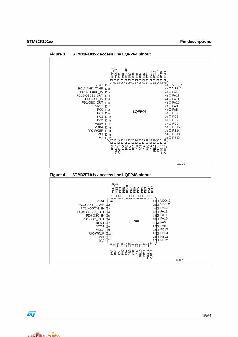
Figure 3. STM32F101xx access line LQFP64 pinout
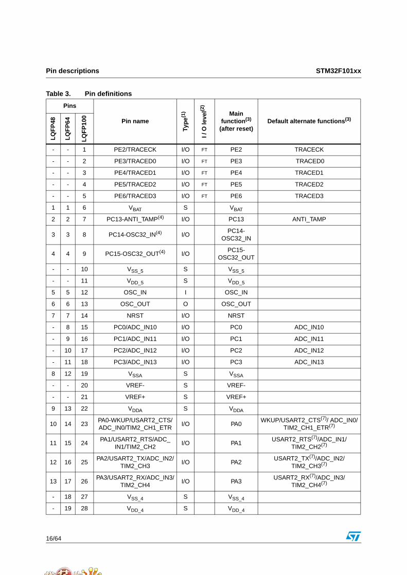
Figure 4. STM32F101xx access line LQFP48 pinout
64 63 62 61 60 59 58 57 56 55 54 53 52 51 50 494847
46 45 44 4342414039383736353433
17 18 19 20 21 22 23 24 29 30 31 3225 26 27 28
123456 7 8 9 1011 12 13141516
VBATPC13-ANTI_TAMP
PC14-OSC32_INPC15-OSC32_OUT
PD0 OSC_INPD1 OSC_OUT
NRSTPC0PC1PC2PC3
VSSAVDDA
PA0-WKUPPA1PA2
VD
D_3
V
SS
_3
PB
9
PB
8
BO
OT
0
PB
7
PB
6
PB
5
PB
4
PB
3
PD
2
PC
12
PC
11
PC
10
PA15
PA
14
VDD_2 VSS_2 PA13 PA12 PA11 PA10 PA9 PA8 PC9 PC8 PC7 PC6 PB15 PB14 PB13 PB12
PA3
VS
S_4
VD
D_4
PA4
PA5
PA6
PA7
PC
4P
C5
PB
0P
B1
PB
2P
B10
PB
11V
SS
_1V
DD
_1
LQFP64
ai14387
44 43 42 41 40 39 38 3736
35
343332
31
30
2928
27
2625
242312
13 14 15 16 17 18 19 20 21 22
1
2
3
4
5
6
7
8
9
10
11
48 47 46 45
LQFP48
PA3
PA4
PA5
PA6
PA7
PB
0P
B1
PB
2P
B10
PB
11V
SS
_1V
DD
_1
VDD_2 VSS_2 PA13 PA12 PA11 PA10 PA9 PA8 PB15 PB14 PB13 PB12
VBATPC13-ANTI_TAMP
PC14-OSC32_INPC15-OSC32_OUT
PD0 OSC_INPD1 OSC_OUT
NRSTVSSAVDDA
PA0-WKUPPA1PA2
VD
D_3
V
SS
_3
PB
9
PB
8
BO
OT
0
PB
7
PB
6
PB
5
PB
4
PB
3
PA15
PA
14
ai14378
Pin descriptions STM32F101xx
16/64
Table 3. Pin definitions
Pins
Pin name
Typ
e(1)
I / O
leve
l(2)
Main function(3)
(after reset)Default alternate functions(3)
LQ
FP
48
LQ
FP
64
LQ
FP
100
- - 1 PE2/TRACECK I/O FT PE2 TRACECK
- - 2 PE3/TRACED0 I/O FT PE3 TRACED0
- - 3 PE4/TRACED1 I/O FT PE4 TRACED1
- - 4 PE5/TRACED2 I/O FT PE5 TRACED2
- - 5 PE6/TRACED3 I/O FT PE6 TRACED3
1 1 6 VBAT S VBAT
2 2 7 PC13-ANTI_TAMP(4) I/O PC13 ANTI_TAMP
3 3 8 PC14-OSC32_IN(4) I/OPC14-
OSC32_IN
4 4 9 PC15-OSC32_OUT(4) I/OPC15-
OSC32_OUT
- - 10 VSS_5 S VSS_5
- - 11 VDD_5 S VDD_5
5 5 12 OSC_IN I OSC_IN
6 6 13 OSC_OUT O OSC_OUT
7 7 14 NRST I/O NRST
- 8 15 PC0/ADC_IN10 I/O PC0 ADC_IN10
- 9 16 PC1/ADC_IN11 I/O PC1 ADC_IN11
- 10 17 PC2/ADC_IN12 I/O PC2 ADC_IN12
- 11 18 PC3/ADC_IN13 I/O PC3 ADC_IN13
8 12 19 VSSA S VSSA
- - 20 VREF- S VREF-
- - 21 VREF+ S VREF+
9 13 22 VDDA S VDDA
10 14 23PA0-WKUP/USART2_CTS/ADC_IN0/TIM2_CH1_ETR
I/O PA0WKUP/USART2_CTS(7)/ ADC_IN0/
TIM2_CH1_ETR(7)
11 15 24PA1/USART2_RTS/ADC_
IN1/TIM2_CH2 I/O PA1
USART2_RTS(7)/ADC_IN1/TIM2_CH2(7)
12 16 25PA2/USART2_TX/ADC_IN2/
TIM2_CH3 I/O PA2
USART2_TX(7)/ADC_IN2/TIM2_CH3(7)
13 17 26PA3/USART2_RX/ADC_IN3/
TIM2_CH4 I/O PA3
USART2_RX(7)/ADC_IN3/TIM2_CH4(7)
- 18 27 VSS_4 S VSS_4
- 19 28 VDD_4 S VDD_4
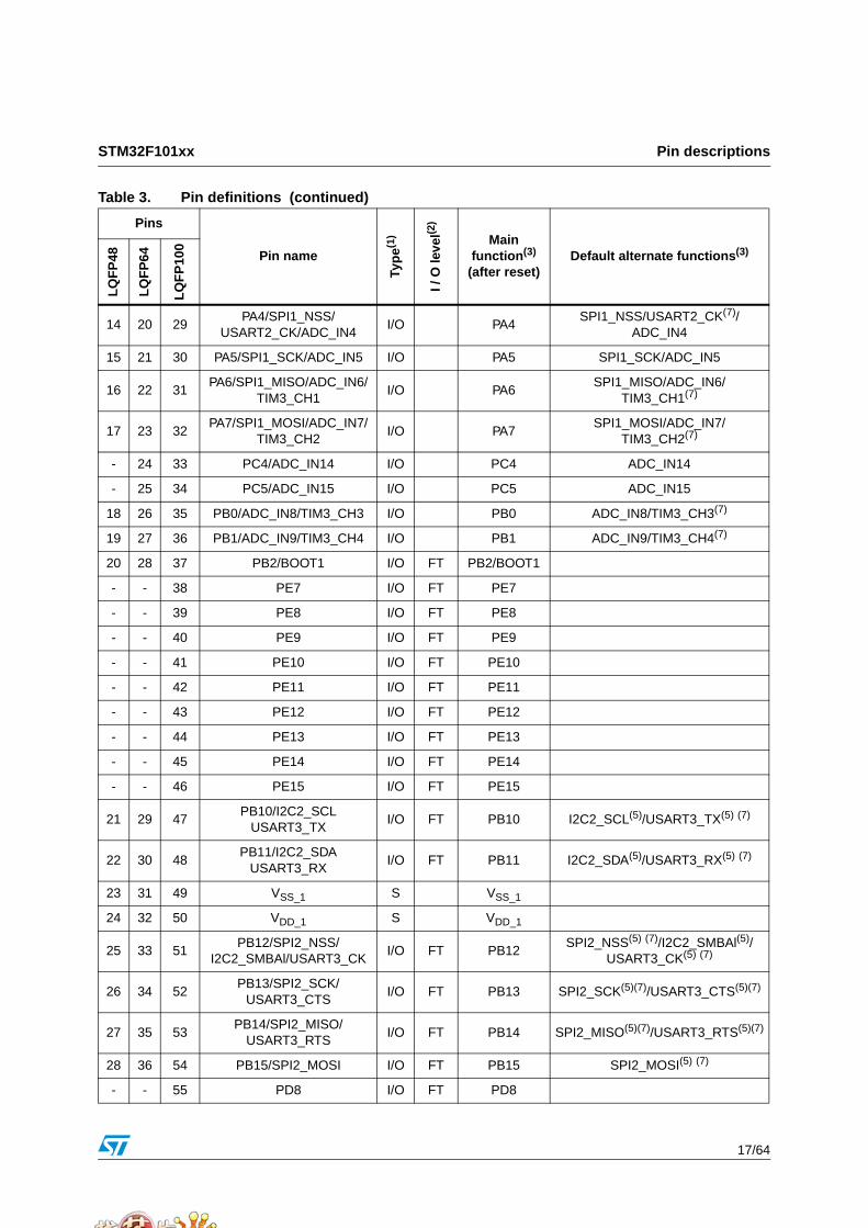
STM32F101xx Pin descriptions
17/64
14 20 29PA4/SPI1_NSS/
USART2_CK/ADC_IN4 I/O PA4
SPI1_NSS/USART2_CK(7)/ADC_IN4
15 21 30 PA5/SPI1_SCK/ADC_IN5 I/O PA5 SPI1_SCK/ADC_IN5
16 22 31PA6/SPI1_MISO/ADC_IN6/
TIM3_CH1 I/O PA6
SPI1_MISO/ADC_IN6/TIM3_CH1(7)
17 23 32PA7/SPI1_MOSI/ADC_IN7/
TIM3_CH2 I/O PA7
SPI1_MOSI/ADC_IN7/TIM3_CH2(7)
- 24 33 PC4/ADC_IN14 I/O PC4 ADC_IN14
- 25 34 PC5/ADC_IN15 I/O PC5 ADC_IN15
18 26 35 PB0/ADC_IN8/TIM3_CH3 I/O PB0 ADC_IN8/TIM3_CH3(7)
19 27 36 PB1/ADC_IN9/TIM3_CH4 I/O PB1 ADC_IN9/TIM3_CH4(7)
20 28 37 PB2/BOOT1 I/O FT PB2/BOOT1
- - 38 PE7 I/O FT PE7
- - 39 PE8 I/O FT PE8
- - 40 PE9 I/O FT PE9
- - 41 PE10 I/O FT PE10
- - 42 PE11 I/O FT PE11
- - 43 PE12 I/O FT PE12
- - 44 PE13 I/O FT PE13
- - 45 PE14 I/O FT PE14
- - 46 PE15 I/O FT PE15
21 29 47PB10/I2C2_SCL
USART3_TX I/O FT PB10 I2C2_SCL(5)/USART3_TX(5) (7)
22 30 48PB11/I2C2_SDA
USART3_RX I/O FT PB11 I2C2_SDA(5)/USART3_RX(5) (7)
23 31 49 VSS_1 S VSS_1
24 32 50 VDD_1 S VDD_1
25 33 51PB12/SPI2_NSS/
I2C2_SMBAl/USART3_CKI/O FT PB12
SPI2_NSS(5) (7)/I2C2_SMBAl(5)/USART3_CK(5) (7)
26 34 52PB13/SPI2_SCK/
USART3_CTSI/O FT PB13 SPI2_SCK(5)(7)/USART3_CTS(5)(7)
27 35 53PB14/SPI2_MISO/
USART3_RTSI/O FT PB14 SPI2_MISO(5)(7)/USART3_RTS(5)(7)
28 36 54 PB15/SPI2_MOSI I/O FT PB15 SPI2_MOSI(5) (7)
- - 55 PD8 I/O FT PD8
Table 3. Pin definitions (continued)
Pins
Pin name
Typ
e(1)
I / O
leve
l(2)
Main function(3)
(after reset)Default alternate functions(3)
LQ
FP
48
LQ
FP
64
LQ
FP
100
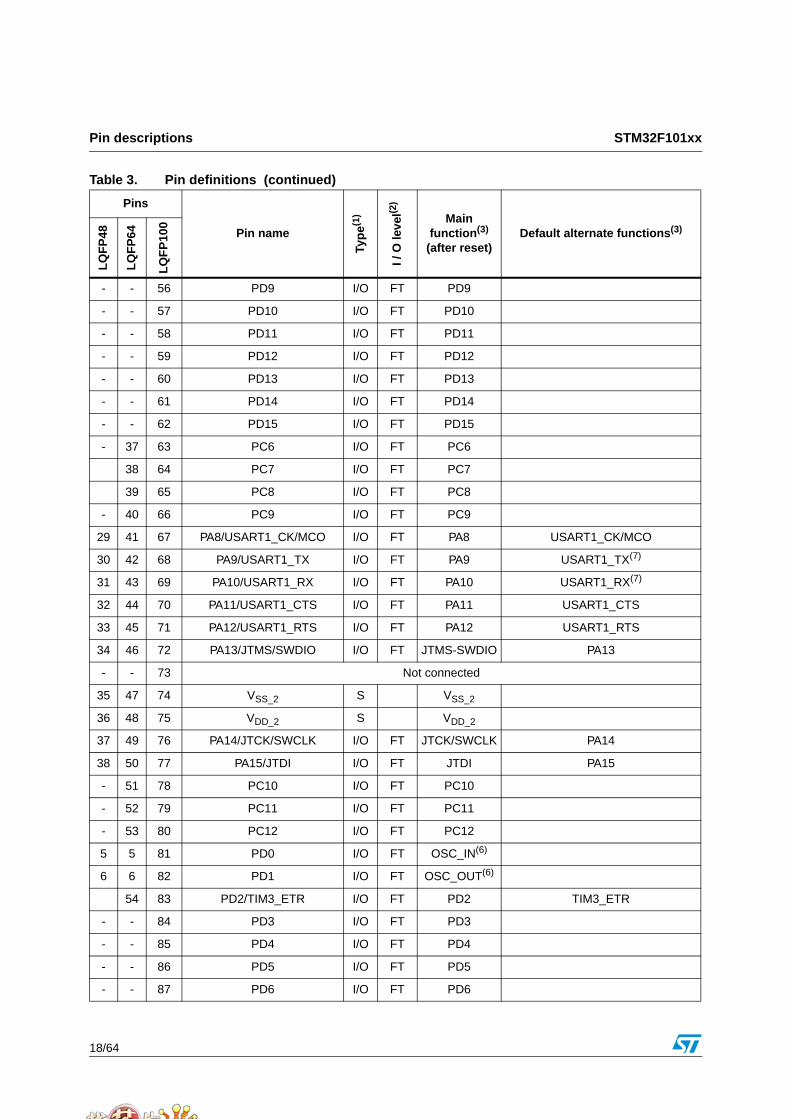
Pin descriptions STM32F101xx
18/64
- - 56 PD9 I/O FT PD9
- - 57 PD10 I/O FT PD10
- - 58 PD11 I/O FT PD11
- - 59 PD12 I/O FT PD12
- - 60 PD13 I/O FT PD13
- - 61 PD14 I/O FT PD14
- - 62 PD15 I/O FT PD15
- 37 63 PC6 I/O FT PC6
38 64 PC7 I/O FT PC7
39 65 PC8 I/O FT PC8
- 40 66 PC9 I/O FT PC9
29 41 67 PA8/USART1_CK/MCO I/O FT PA8 USART1_CK/MCO
30 42 68 PA9/USART1_TX I/O FT PA9 USART1_TX(7)
31 43 69 PA10/USART1_RX I/O FT PA10 USART1_RX(7)
32 44 70 PA11/USART1_CTS I/O FT PA11 USART1_CTS
33 45 71 PA12/USART1_RTS I/O FT PA12 USART1_RTS
34 46 72 PA13/JTMS/SWDIO I/O FT JTMS-SWDIO PA13
- - 73 Not connected
35 47 74 VSS_2 S VSS_2
36 48 75 VDD_2 S VDD_2
37 49 76 PA14/JTCK/SWCLK I/O FT JTCK/SWCLK PA14
38 50 77 PA15/JTDI I/O FT JTDI PA15
- 51 78 PC10 I/O FT PC10
- 52 79 PC11 I/O FT PC11
- 53 80 PC12 I/O FT PC12
5 5 81 PD0 I/O FT OSC_IN(6)
6 6 82 PD1 I/O FT OSC_OUT(6)
54 83 PD2/TIM3_ETR I/O FT PD2 TIM3_ETR
- - 84 PD3 I/O FT PD3
- - 85 PD4 I/O FT PD4
- - 86 PD5 I/O FT PD5
- - 87 PD6 I/O FT PD6
Table 3. Pin definitions (continued)
Pins
Pin name
Typ
e(1)
I / O
leve
l(2)
Main function(3)
(after reset)Default alternate functions(3)
LQ
FP
48
LQ
FP
64
LQ
FP
100
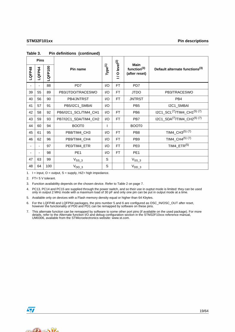
STM32F101xx Pin descriptions
19/64
- - 88 PD7 I/O FT PD7
39 55 89 PB3/JTDO/TRACESWO I/O FT JTDO PB3/TRACESWO
40 56 90 PB4/JNTRST I/O FT JNTRST PB4
41 57 91 PB5/I2C1_SMBAl I/O PB5 I2C1_SMBAl
42 58 92 PB6/I2C1_SCL/TIM4_CH1 I/O FT PB6 I2C1_SCL(7)/TIM4_CH1(5) (7)
43 59 93 PB7/I2C1_SDA/TIM4_CH2 I/O FT PB7 I2C1_SDA(7)/TIM4_CH2(5) (7)
44 60 94 BOOT0 I BOOT0
45 61 95 PB8/TIM4_CH3 I/O FT PB8 TIM4_CH3(5) (7)
46 62 96 PB9/TIM4_CH4 I/O FT PB9 TIM4_CH4(5) (7)
- - 97 PE0/TIM4_ETR I/O FT PE0 TIM4_ETR(5)
- - 98 PE1 I/O FT PE1
47 63 99 VSS_3 S VSS_3
48 64 100 VDD_3 S VDD_3
1. I = input, O = output, S = supply, HiZ= high impedance.
2. FT= 5 V tolerant.
3. Function availability depends on the chosen device. Refer to Table 2 on page 7.
4. PC13, PC14 and PC15 are supplied through the power switch, and so their use in ouptut mode is limited: they can be used only in output 2 MHz mode with a maximum load of 30 pF and only one pin can be put in output mode at a time.
5. Available only on devices with a Flash memory density equal or higher than 64 Kbytes.
6. For the LQFP48 and LQFP64 packages, the pins number 5 and 6 are configured as OSC_IN/OSC_OUT after reset, however the functionality of PD0 and PD1 can be remapped by software on these pins.
7. This alternate function can be remapped by software to some other port pins (if available on the used package). For more details, refer to the Alternate function I/O and debug configuration section in the STM32F10xxx reference manual, UM0306, available from the STMicroelectronics website: www.st.com.
Table 3. Pin definitions (continued)
Pins
Pin name
Typ
e(1)
I / O
leve
l(2)
Main function(3)
(after reset)Default alternate functions(3)
LQ
FP
48
LQ
FP
64
LQ
FP
100
Memory mapping STM32F101xx
20/64
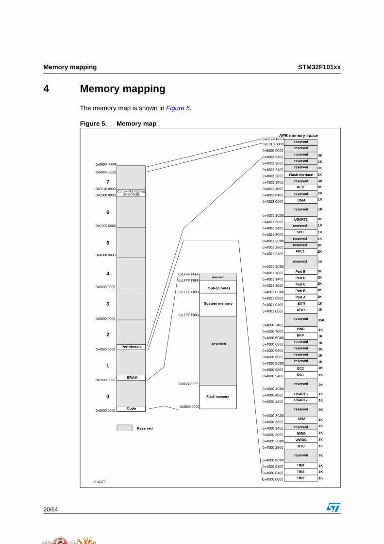
4 Memory mapping
The memory map is shown in Figure 5.
Figure 5. Memory map
1K
APB memory space
DMA
RTC
WWDG
IWDG
SPI2
USART2
USART3
ADC1
USART1
SPI1
1K
35K
1K
1K
2K
1K
1K
2K
1K
1K
1K
1K
1K
7K
1K
Port E
1K
1K
1K
3K
1K
1K
1K
1K
1K
1K
1K
1K
2K
1K
1K
1K
I2C2
EXTI
RCC
1K
1K
1K
1K
1K
1K
1K
1K
3K
1K
3K
1K
4K
0
1
2
3
4
5
6
7
Code
Peripherals
SRAM
reserved
reserved
Option bytes
Reserved
0x4000 0000
0x4000 0400
0x4000 0800
0x4000 0C00
0x4000 2800
0x4000 2C00
0x4000 3000
0x4000 3400
0x4000 3800
0x4000 3C00
0x4000 4400
0x4000 4800
0x4000 4C00
0x4000 5400
0x4000 5800
0x4000 5C00
0x4000 6000
0x4000 6400
0x4000 6800
0x4000 6C00
0x4000 7000
0x4000 7400
0x4001 0000
0x4001 0400
0x4001 0800
0x4001 0C00
0x4001 1000
0x4001 1400
0x4001 1800
0x4001 1C00
0x4001 2400
0x4001 2800
0x4001 2C00
0x4001 3000
0x4001 3400
0x4001 3800
0x4001 3C00
0x4002 0000
0x4002 0400
0x4002 1000
0x4002 1400
0x4002 2000
0x4002 2400
0x4002 3000
0x4002 3400
0x6000 0000
0xE010 00000xFFFF FFFF
reserved
reserved
reserved
reserved
reserved
reserved
Flash interface
reserved
reserved
reserved
reserved
reserved
reserved
reserved
Port D
Port C
Port B
Port A
AFIO
PWR
BKP
reserved
reserved
reserved
reserved
I2C1
reserved
reserved
reserved
reserved
TIM4
TIM3
TIM2
0xFFFF FFFF
0xFFFF F000
0xE010 0000
0xE000 0000
0xC000 0000
0xA000 0000
0x8000 0000
0x6000 0000
0x4000 0000
0x2000 0000
0x0000 0000
0x1FFF FFFF
0x1FFF F9FF
0x1FFF F800
0x1FFF F000
0x0801 FFFF
0x0800 0000
System memory
Flash memory
Cortex-M3 internalperipherals
ai14379
STM32F101xx Electrical characteristics
21/64
5 Electrical characteristics
5.1 Test conditionsUnless otherwise specified, all voltages are referred to VSS.
5.1.1 Minimum and maximum values
Unless otherwise specified the minimum and maximum values are guaranteed in the worst conditions of ambient temperature, supply voltage and frequencies by tests in production on 100% of the devices with an ambient temperature at TA = 25 °C and TA = TAmax (given by the selected temperature range).
Data based on characterization results, design simulation and/or technology characteristics are indicated in the table footnotes and are not tested in production. Based on characterization, the minimum and maximum values refer to sample tests and represent the mean value plus or minus three times the standard deviation (mean±3Σ).
5.1.2 Typical values
Unless otherwise specified, typical data are based on TA = 25 °C, VDD = 3.3 V (for the 2 V ≤VDD ≤3.6 V voltage range). They are given only as design guidelines and are not tested.
Typical ADC accuracy values are determined by characterization of a batch of samples from a standard diffusion lot over the full temperature range, where 95% of the devices have an error less than or equal to the value indicated (mean±2Σ).
5.1.3 Typical curves
Unless otherwise specified, all typical curves are given only as design guidelines and are not tested.
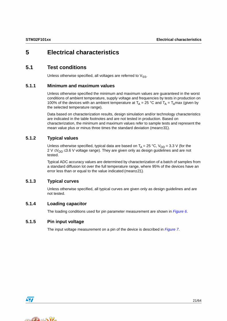
5.1.4 Loading capacitor
The loading conditions used for pin parameter measurement are shown in Figure 6.
5.1.5 Pin input voltage
The input voltage measurement on a pin of the device is described in Figure 7.
Electrical characteristics STM32F101xx
22/64
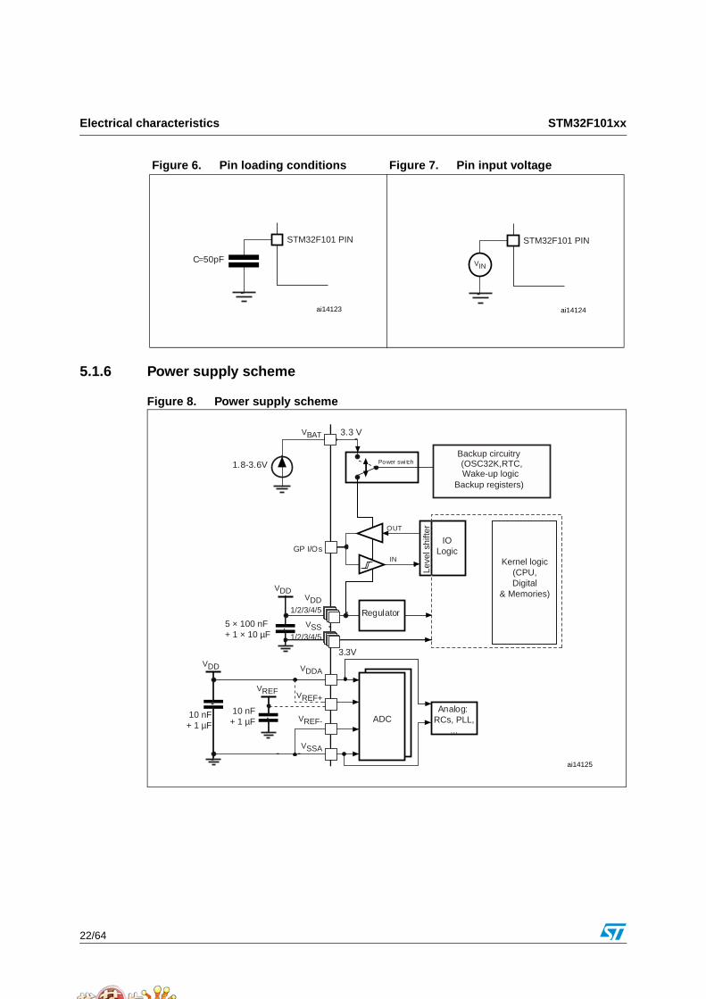
5.1.6 Power supply scheme
Figure 8. Power supply scheme
Figure 6. Pin loading conditions Figure 7. Pin input voltage
ai14123
C=50pF
STM32F101 PIN
ai14124
STM32F101 PIN
VIN
ai14125
3.3V
VDD1/2/3/4/5
Analog: RCs, PLL,
...
Power swi tch
VBAT 3.3 V
GP I/Os
OUT
IN Kernel logic (CPU, Digital
& Memories)
Backup circuitry(OSC32K,RTC,
Backup registers)Wake-up logic
5 × 100 nF+ 1 × 10 µF
1.8-3.6V
RegulatorVSS
1/2/3/4/5
VDDA
VREF+
VREF-
VSSA
ADC
Leve
l shi
fter
IOLogic
VDD
10 nF+ 1 µF
VREF
10 nF+ 1 µF
VDD
STM32F101xx Electrical characteristics
23/64
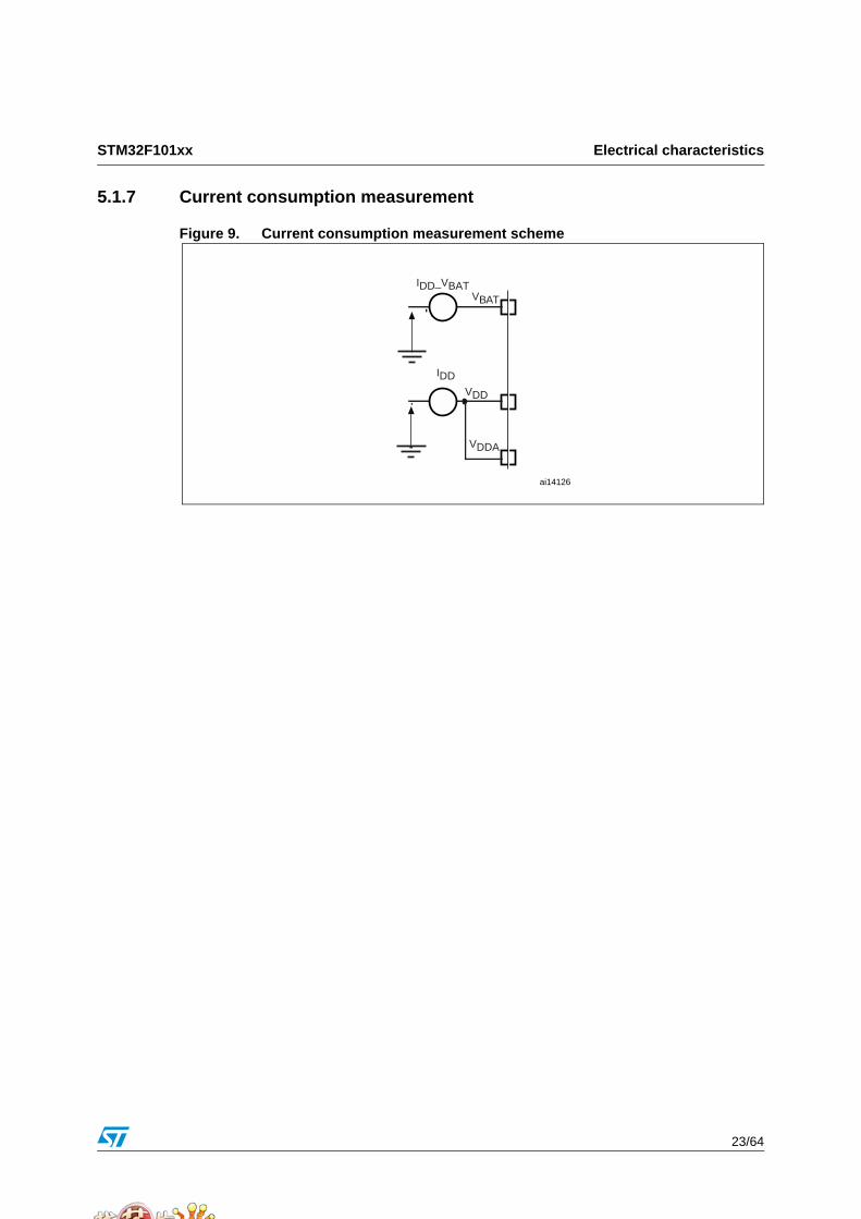
5.1.7 Current consumption measurement
Figure 9. Current consumption measurement scheme
ai14126
VBAT
VDD
VDDA
IDD_VBAT
IDD
Electrical characteristics STM32F101xx
24/64
5.2 Absolute maximum ratingsStresses above the absolute maximum ratings listed in Table 4: Voltage characteristics, Table 5: Current characteristics, and Table 6: Thermal characteristics may cause permanent damage to the device. These are stress ratings only and functional operation of the device at these conditions is not implied. Exposure to maximum rating conditions for extended periods may affect device reliability.
Table 4. Voltage characteristics
Symbol Ratings Min Max Unit
VDD−VSSExternal 3.3 V supply voltage (including VDDA and VDD)(1)
1. All 3.3 V power (VDD, VDDA) and ground (VSS, VSSA) pins must always be connected to the external 3.3 V supply.
−0.3 4.0
V
VIN
Input voltage on five volt tolerant pin(2)
2. IINJ(PIN) must never be exceeded (see Table 5: Current characteristics). This is implicitly insured if VIN maximum is respected. If VIN maximum cannot be respected, the injection current must be limited externally to the IINJ(PIN) value. A positive injection is induced by VIN>VDD while a negative injection is induced by VIN<VSS.
VSS − 0.3 +5.5
Input voltage on any other pin(2) VSS − 0.3 VDD+0.3
|∆VDDx| Variations between different power pins 50 50
mV|VSSX − VSS|
Variations between all the different ground pins
50 50
VESD(HBM)Electrostatic discharge voltage (human body model)
see Section 5.3.11: Absolute maximum ratings (electrical
sensitivity)
Table 5. Current characteristics
Symbol Ratings Max. Unit
IVDD Total current into VDD power lines (source)(1)
1. All 3.3 V power (VDD, VDDA) and ground (VSS, VSSA) pins must always be connected to the external 3.3 V supply.
150
mA
IVSS Total current out of VSS ground lines (sink)(1) 150
IIOOutput current sunk by any I/O and control pin 25
Output current source by any I/Os and control pin − 25
IINJ(PIN) (2)(3)
2. IINJ(PIN) must never be exceeded. This is implicitly insured if VIN maximum is respected. If VIN maximum cannot be respected, the injection current must be limited externally to the IINJ(PIN) value. A positive injection is induced by VIN>VDD while a negative injection is induced by VIN<VSS.
3. Negative injection disturbs the analog performance of the device. See note in Section 5.3.16: 12-bit ADC characteristics.
Injected current on NRST pin ± 5
Injected current on High-speed external OSC_IN and Low-speed external OSC_IN pins
± 5
Injected current on any other pin(4)
4. When several inputs are submitted to a current injection, the maximum ΣIINJ(PIN) is the absolute sum of the positive and negative injected currents (instantaneous values). These results are based on characterization with ΣIINJ(PIN) maximum current injection on four I/O port pins of the device.
± 5
ΣIINJ(PIN)(2) Total injected current (sum of all I/O and control pins)(4) ± 25

STM32F101xx Electrical characteristics
25/64
Table 6. Thermal characteristics
Symbol Ratings Value Unit
TSTG Storage temperature range –65 to +150 °C
TJ Maximum junction temperature (see Thermal characteristics)
Electrical characteristics STM32F101xx
26/64
5.3 Operating conditions
5.3.1 General operating conditions
5.3.2 Operating conditions at power-up / power-down
The parameters given in Table 8 are derived from tests performed under the ambient temperature condition summarized in Table 7.
Table 8. Operating conditions at power-up / power-down
Table 7. General operating conditions
Symbol Parameter Conditions Min Max Unit
fHCLK Internal AHB clock frequency 0 36
MHzfPCLK1 Internal APB1 clock frequency 0 36
fPCLK2 Internal APB2 clock frequency 0 36
VDD Standard operating voltage 2 3.6 V
VBAT Backup operating voltage 1.8 3.6 V
TA Ambient temperature range −40 85 °C
Symbol Parameter Conditions Min Typ Max Unit
tVDD VDD rise/fall time 20 µs/V
20 ms/V
STM32F101xx Electrical characteristics
27/64
5.3.3 Embedded reset and power control block characteristics
The parameters given in Table 9 are derived from tests performed under ambient temperature and VDD supply voltage conditions summarized in Table 7.
.
5.3.4 Embedded reference voltage
The parameters given in Table 10 are derived from tests performed under ambient temperature and VDD supply voltage conditions summarized in Table 7.
Table 9. Embedded reset and power control block characteristics
Symbol Parameter Conditions Min Typ Max Unit
VPVDProgrammable voltage detector level selection
PLS[2:0]=000 (rising edge) 2.1 2.18 2.26 V
PLS[2:0]=000 (falling edge) 2 2.08 2.16 V
PLS[2:0]=001 (rising edge) 2.19 2.28 2.37 V
PLS[2:0]=001 (falling edge) 2.09 2.18 2.27 V
PLS[2:0]=010 (rising edge) 2.28 2.38 2.48 V
PLS[2:0]=010 (falling edge) 2.18 2.28 2.38 V
PLS[2:0]=011 (rising edge) 2.38 2.48 2.58 V
PLS[2:0]=011 (falling edge) 2.28 2.38 2.48 V
PLS[2:0]=100 (rising edge) 2.47 2.58 2.69 V
PLS[2:0]=100 (falling edge) 2.37 2.48 2.59 V
PLS[2:0]=101 (rising edge) 2.57 2.68 2.79 V
PLS[2:0]=101 (falling edge) 2.47 2.58 2.69 V
PLS[2:0]=110 (rising edge) 2.66 2.78 2.9 V
PLS[2:0]=110 (falling edge) 2.56 2.68 2.8 V
PLS[2:0]=111 (rising edge) 2.76 2.88 3 V
PLS[2:0]=111 (falling edge) 2.66 2.78 2.9 V
VPVDhyst PVD hysteresis 100 mV
VPOR/PDRPower on/power down reset threshold
Falling edge 1.8 1.88 1.96 V
Rising edge 1.84 1.92 2.0 V
VPDRhyst PDR hysteresis 40 mV
tRSTTEMPO Reset temporization 1.5 2.5 3.5 ms
Table 10. Embedded internal reference voltage
Symbol Parameter Conditions Min Typ Max Unit
VREFINT Internal reference voltage -45 °C < TA < +85 °C 1.16 1.20 1.24 V
Electrical characteristics STM32F101xx
28/64
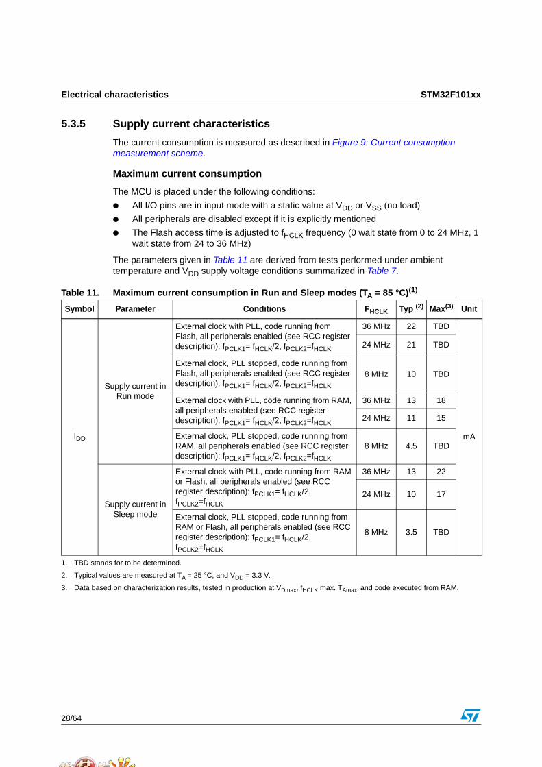
5.3.5 Supply current characteristics
The current consumption is measured as described in Figure 9: Current consumption measurement scheme.
Maximum current consumption
The MCU is placed under the following conditions:
All I/O pins are in input mode with a static value at VDD or VSS (no load)
All peripherals are disabled except if it is explicitly mentioned
The Flash access time is adjusted to fHCLK frequency (0 wait state from 0 to 24 MHz, 1 wait state from 24 to 36 MHz)
The parameters given in Table 11 are derived from tests performed under ambient temperature and VDD supply voltage conditions summarized in Table 7.
Table 11. Maximum current consumption in Run and Sleep modes (TA = 85 °C)(1)
Symbol Parameter Conditions FHCLK Typ (2) Max(3) Unit
IDD
Supply current in Run mode
External clock with PLL, code running from Flash, all peripherals enabled (see RCC register description): fPCLK1= fHCLK/2, fPCLK2=fHCLK
36 MHz 22 TBD
mA
24 MHz 21 TBD
External clock, PLL stopped, code running from Flash, all peripherals enabled (see RCC register description): fPCLK1= fHCLK/2, fPCLK2=fHCLK
8 MHz 10 TBD
External clock with PLL, code running from RAM, all peripherals enabled (see RCC register description): fPCLK1= fHCLK/2, fPCLK2=fHCLK
36 MHz 13 18
24 MHz 11 15
External clock, PLL stopped, code running from RAM, all peripherals enabled (see RCC register description): fPCLK1= fHCLK/2, fPCLK2=fHCLK
8 MHz 4.5 TBD
Supply current in Sleep mode
External clock with PLL, code running from RAM or Flash, all peripherals enabled (see RCC register description): fPCLK1= fHCLK/2, fPCLK2=fHCLK
36 MHz 13 22
24 MHz 10 17
External clock, PLL stopped, code running from RAM or Flash, all peripherals enabled (see RCC register description): fPCLK1= fHCLK/2, fPCLK2=fHCLK
8 MHz 3.5 TBD
1. TBD stands for to be determined.
2. Typical values are measured at TA = 25 °C, and VDD = 3.3 V.
3. Data based on characterization results, tested in production at VDmax, fHCLK max. TAmax, and code executed from RAM.
STM32F101xx Electrical characteristics
29/64
Table 12. Maximum current consumption in Stop and Standby modes(1)
Symbol Parameter Conditions
Typ(2) Max(3)
UnitVDD/ VBAT = 2.4 V
VDD/VBAT= 3.3 V
TA = 85 °C
IDD
Supply current in Stop mode
Regulator in Run mode, Low-speed and high-speed internal
RC oscillators and high-speed oscillator OFF (no independent
watchdog)
TBD 24 TBD
µA
Regulator in Low Power mode, Low-speed and high-speed internal
RC oscillators and high-speed oscillator OFF (no independent
watchdog)
TBD(4) 14(4) TBD(4)
Supply current in Standby mode(5)
Low-speed internal RC oscillator and independent watchdog OFF, low-speed oscillator and RTC OFF
TBD(4) 2(4) TBD(4)
IDD_VBA
T
Backup domain supply current
Low-speed oscillator and RTC ON 1(4) 1.4(4) TBD(4)
1. TBD stands for to be determined.
2. Typical values are measured at TA = 25 °C, VDD = 3.3 V, unless otherwise specified.
3. Data based on characterization results, tested in production at VDD max, fHCLK max. and TA max.
4. Values expected for next silicon revision.
5. To have the Standby consumption with RTC ON, add IDD_VBAT (Low-speed oscillator and RTC ON) to IDD Standby (when VDD is present the Backup Domain is powered by VDD supply).
Electrical characteristics STM32F101xx
30/64
Typical current consumption
The MCU is placed under the following conditions:
All I/O pins are in input mode with a static value at VDD or VSS (no load)
All peripherals are disabled except if it is explicitly mentioned
The Flash access time is adjusted to fHCLK frequency (0 wait state from 0 to 24 MHz, 1 wait state from 24 to 36 MHz)
The parameters given in Table 13 are derived from tests performed under ambient temperature and VDD supply voltage conditions summarized in Table 7.
Table 13. Typical current consumption in Run and Sleep modes(1)
Symbol Parameter Conditions fHCLK Typ(2) Unit
IDD
Supply current in Run mode
Oscillator running at 8 MHz with PLL, code running from Flash, all peripheral disabled (see RCC register description): fPCLK1= fHCLK/2, fPCLK2 = fHCLK
36 MHz TBD
mA24 MHz 13
16 MHz TBD
Running on HSI clock, code running from Flash, all peripheral disabled (see RCC register description): fPCLK1= fHCLK/2, fPCLK2 = fHCLK. AHB pre-scaler used to reduce the frequency
8 MHz 7.8
mA
4 MHz 7
2 MHz 6.3
1 MHz 6.2
500 kHz 6.1
125 kHz 5.95
Running on HSI clock, code running from RAM, all peripheral disabled (see RCC register description): fPCLK1= fHCLK/2, fPCLK2 = fHCLK. AHB pre-scaler used to reduce the frequency
8 MHz 2.3
mA
4 MHz 1.6
2 MHz 1.2
1 MHz 1
500 kHz 0.88
125 kHz 0.82
Supply current in Sleep mode
Oscillator running at 8 MHz with PLL, code running from Flash, all peripheral disabled (see RCC register description): fPCLK1= fHCLK/2, fPCLK2 = fHCLK
36 MHz TBD
mA24 MHz TBD
16 MHz 1
Running on HSI clock, code running from Flash, all peripheral disabled (see RCC register description): fPCLK1= fHCLK/2, fPCLK2 = fHCLK. AHB pre-scaler used to reduce the frequency
8 MHz TBD
mA
4 MHz TBD
2 MHz TBD
1 MHz TBD
500 kHz TBD
1. TBD stands for to be determined.
2. Typical values are measures at TA = 25 °C, VDD = 3.3 V.
STM32F101xx Electrical characteristics
31/64
Table 14. Typical current consumption in Stop and Standby modes(1)
Symbol Parameter Conditions VDD Typ(2) Unit
IDD
Supply current in Stop mode
Regulator in Run mode,Low-speed and high-speed internal RC oscillators OFFHigh-speed oscillator OFF (no independent watchdog)
3.3 V 24
µA
2.4 V TBD
Regulator in Low Power mode,Low-speed and high-speed internal RC oscillators OFF, High-speed oscillator OFF (no independent watchdog)
3.3 V 14(3)
2.4 V TBD(3)
Supply current in Standby mode(4)
Low-speed internal RC oscillator and independent watchdog OFF
3.3 V 2(3)
µA
2.4 V TBD(3)
Low-speed internal RC oscillator and independent watchdog ON
3.3 V 3.1(3)
2.4 V TBD(3)
Low-speed internal RC oscillator ON, independent watchdog OFF
3.3 V 2.9(3)
2.4 V TBD(3)
IDD_VBATBackup domain supply current
Low-speed oscillator and RTC ON3.3 V 1.4(3)
µA2.4 V 1(3)
Low-speed oscillator OFF, RTC ON3.3 V 0.5(3)
2.4 V TBD(3)
1. TBD stands for to be determined.
2. Typical values are measures at TA = 25 °C, VDD = 3.3 V.
3. Values expected for next silicon revision.
4. To obtain Standby consumption with RTC ON, add IDD_VBAT (Low-speed oscillator, RTC ON) to IDD Standby.
Electrical characteristics STM32F101xx
32/64
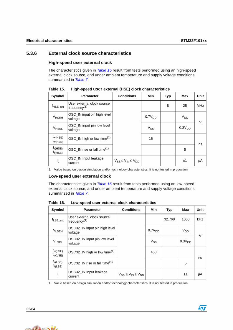
5.3.6 External clock source characteristics
High-speed user external clock
The characteristics given in Table 15 result from tests performed using an high-speed external clock source, and under ambient temperature and supply voltage conditions summarized in Table 7.
Low-speed user external clock
The characteristics given in Table 16 result from tests performed using an low-speed external clock source, and under ambient temperature and supply voltage conditions summarized in Table 7.
Table 15. High-speed user external (HSE) clock characteristics
Symbol Parameter Conditions Min Typ Max Unit
fHSE_extUser external clock source frequency(1)
1. Value based on design simulation and/or technology characteristics. It is not tested in production.
8 25 MHz
VHSEHOSC_IN input pin high level voltage
0.7VDD VDD
V
VHSELOSC_IN input pin low level voltage
VSS 0.3VDD
tw(HSE)tw(HSE)
OSC_IN high or low time(1) 16
nstr(HSE)tf(HSE)
OSC_IN rise or fall time(1) 5
ILOSC_IN Input leakage current
VSS ≤ VIN ≤ VDD ±1 µA
Table 16. Low-speed user external clock characteristics
Symbol Parameter Conditions Min Typ Max Unit
fLSE_extUser external clock source frequency(1)
1. Value based on design simulation and/or technology characteristics. It is not tested in production.
32.768 1000 kHz
VLSEHOSC32_IN input pin high level voltage
0.7VDD VDD
V
VLSELOSC32_IN input pin low level voltage
VSS 0.3VDD
tw(LSE)tw(LSE)
OSC32_IN high or low time(1) 450
nstr(LSE)tf(LSE)
OSC32_IN rise or fall time(1) 5
ILOSC32_IN Input leakage current
VSS ≤ VIN ≤ VDD ±1 µA
STM32F101xx Electrical characteristics
33/64
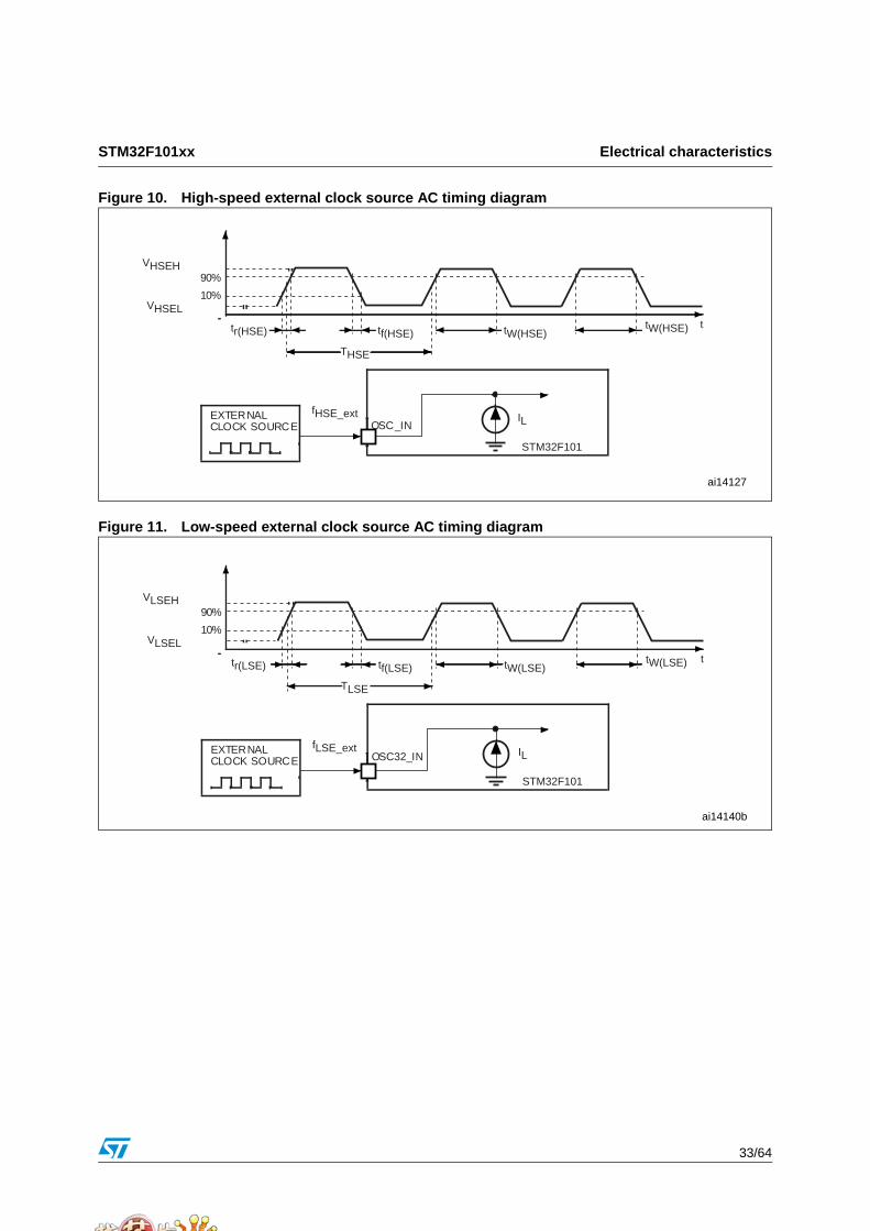
Figure 10. High-speed external clock source AC timing diagram
Figure 11. Low-speed external clock source AC timing diagram
ai14127
OSC_INEXTERNAL
STM32F101
CLOCK SOURCE
VHSEH
tf(HSE) tW(HSE)
IL
90%
10%
THSE
ttr(HSE)tW(HSE)
fHSE_ext
VHSEL
ai14140b
OSC32_INEXTERNAL
STM32F101
CLOCK SOURCE
VLSEH
tf(LSE) tW(LSE)
IL
90%
10%
TLSE
ttr(LSE)tW(LSE)
fLSE_ext
VLSEL
Electrical characteristics STM32F101xx
34/64
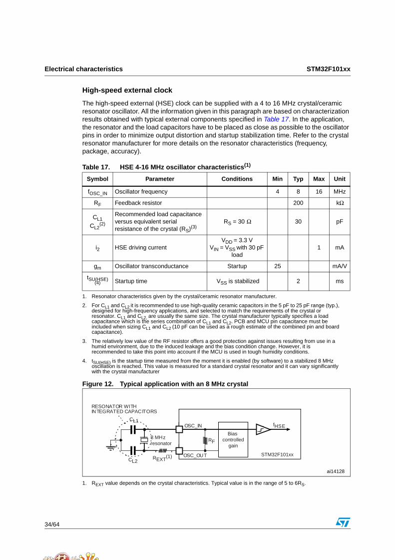
High-speed external clock
The high-speed external (HSE) clock can be supplied with a 4 to 16 MHz crystal/ceramic resonator oscillator. All the information given in this paragraph are based on characterization results obtained with typical external components specified in Table 17. In the application, the resonator and the load capacitors have to be placed as close as possible to the oscillator pins in order to minimize output distortion and startup stabilization time. Refer to the crystal resonator manufacturer for more details on the resonator characteristics (frequency, package, accuracy).
Figure 12. Typical application with an 8 MHz crystal
1. REXT value depends on the crystal characteristics. Typical value is in the range of 5 to 6RS.
Table 17. HSE 4-16 MHz oscillator characteristics(1)
1. Resonator characteristics given by the crystal/ceramic resonator manufacturer.
Symbol Parameter Conditions Min Typ Max Unit
fOSC_IN Oscillator frequency 4 8 16 MHz
RF Feedback resistor 200 kΩ
CL1
CL2(2)
2. For CL1 and CL2 it is recommended to use high-quality ceramic capacitors in the 5 pF to 25 pF range (typ.), designed for high-frequency applications, and selected to match the requirements of the crystal or resonator. CL1 and CL2, are usually the same size. The crystal manufacturer typically specifies a load capacitance which is the series combination of CL1 and CL2. PCB and MCU pin capacitance must be included when sizing CL1 and CL2 (10 pF can be used as a rough estimate of the combined pin and board capacitance).
Recommended load capacitance versus equivalent serial resistance of the crystal (RS)(3)
3. The relatively low value of the RF resistor offers a good protection against issues resulting from use in a humid environment, due to the induced leakage and the bias condition change. However, it is recommended to take this point into account if the MCU is used in tough humidity conditions.
RS = 30 Ω 30 pF
i2 HSE driving currentVDD = 3.3 V
VIN = VSS with 30 pF load
1 mA
gm Oscillator transconductance Startup 25 mA/V
tSU(HSE)(4)
4. tSU(HSE) is the startup time measured from the moment it is enabled (by software) to a stabilized 8 MHz oscillation is reached. This value is measured for a standard crystal resonator and it can vary significantly with the crystal manufacturer
Startup time VSS is stabilized 2 ms
ai14128
OSC_OUT
OSC_IN fHSECL1
RF
STM32F101xx
8 MHzresonator
RESONATOR WITHINTEGRATED CAPACITORS
Bias controlled
gain
REXT(1) CL2
STM32F101xx Electrical characteristics
35/64
Low-speed external clock
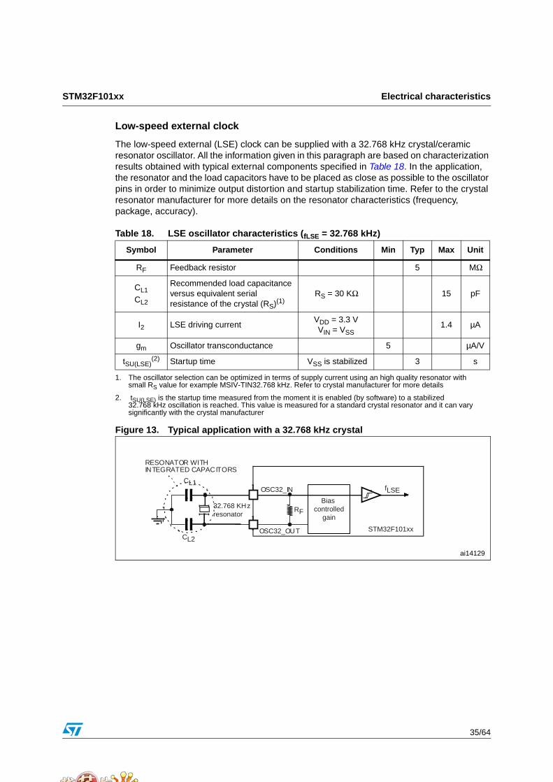
The low-speed external (LSE) clock can be supplied with a 32.768 kHz crystal/ceramic resonator oscillator. All the information given in this paragraph are based on characterization results obtained with typical external components specified in Table 18. In the application, the resonator and the load capacitors have to be placed as close as possible to the oscillator pins in order to minimize output distortion and startup stabilization time. Refer to the crystal resonator manufacturer for more details on the resonator characteristics (frequency, package, accuracy).
Figure 13. Typical application with a 32.768 kHz crystal
Table 18. LSE oscillator characteristics (fLSE = 32.768 kHz)
Symbol Parameter Conditions Min Typ Max Unit
RF Feedback resistor 5 MΩ
CL1
CL2
Recommended load capacitance versus equivalent serial resistance of the crystal (RS)(1)
1. The oscillator selection can be optimized in terms of supply current using an high quality resonator with small RS value for example MSIV-TIN32.768 kHz. Refer to crystal manufacturer for more details
RS = 30 KΩ 15 pF
I2 LSE driving currentVDD = 3.3 VVIN = VSS
1.4 µA
gm Oscillator transconductance 5 µA/V
tSU(LSE)(2)
2. tSU(LSE) is the startup time measured from the moment it is enabled (by software) to a stabilized 32.768 kHz oscillation is reached. This value is measured for a standard crystal resonator and it can vary significantly with the crystal manufacturer
Startup time VSS is stabilized 3 s
ai14129
OSC32_OUT
OSC32_IN fLSECL1
RF
STM32F101xx
32.768 KHzresonator
RESONATOR WITHINTEGRATED CAPACITORS
Bias controlled
gain
CL2
Electrical characteristics STM32F101xx
36/64
5.3.7 Internal Clock source characteristics
The parameters given in Table 19 are derived from tests performed under ambient temperature and VDD supply voltage conditions summarized in Table 7.
High-speed internal (HSI) RC oscillator
LSI Low Speed Internal RC Oscillator
Table 19. HSI oscillator characteristics(1)(2)
1. VDD = 3.3 V, TA = −40 to 85 °C unless otherwise specified.
2. TBD stands for to be determined.
Symbol Parameter Conditions Min Typ Max(3)
3. Values based on device characterization, not tested in production.
Unit
fHSI Frequency 8 MHz
ACCHSI Accuracy of HSI oscillatorTA = –40 to 85 °C TBD ±3 TBD %
at TA = 25 °C TBD ±1 TBD %
tsu(HSI) HSI oscillator startup time 1 2 µs
IDD(HSI)HSI oscillator power consumption
80 100 µA
Table 20. LSI oscillator characteristics (1)
1. VDD = 3 V, TA = −40 to 85 °C unless otherwise specified.
Symbol Parameter Conditions Min Typ Max(2)
2. Value based on device characterization, not tested in production.
Unit
fLSI Frequency 30 60 kHz
tsu(LSI) LSI oscillator start up time 85 µs
IDD(LSI)LSI oscillator power consumption
0.65 1.2 µA
STM32F101xx Electrical characteristics
37/64
Wakeup time from low power mode
The wakeup times given in Table 21 is measured on a wakeup phase with a 8-MHz HSI RC oscillator. The clock source used to wake up the device depends from the current operating mode:
Stop or Standby mode: the clock source is the RC oscillator
Sleep mode: the clock source is the clock that was set before entering Sleep mode.
All timings are derived from tests performed under ambient temperature and VDD supply voltage conditions summarized in Table 7.
5.3.8 PLL characteristics
The parameters given in Table 22 are derived from tests performed under ambient temperature and VDD supply voltage conditions summarized in Table 7.
Table 21. Low-power mode wakeup timings(1)
1. TBD stands for to be determined.
Symbol Parameter Conditions Typ Max Unit
tWUSLEEP(2)
2. The wakeup time from Sleep and Stop mode are measured from the wakeup event to the point in which the user application code reads the first instruction.
Wakeup from Sleep mode Wakeup on HSI RC clock 0.75 TBD µs
tWUSTOP(2)
Wakeup from Stop mode (regulator in run mode)
HSI RC wakeup time = 2 µs 4 TBD
µsWakeup from Stop mode (regulator in low power mode)
HSI RC wakeup time = 2 µs, Regulator wakeup from LP mode time = 5 µs
7 TBD
tWUSTDBY(3)
3. The wakeup time from Standby mode is measured from the wakeup event to the point in which the device exits from reset.
Wakeup from Standby modeHSI RC wakeup time = 2 µs, Regulator wakeup from power down time = 38 µs
40 TBD µs
Table 22. PLL characteristics(1)
1. TBD stands for to be determined.
Symbol Parameter Test
conditions
ValueUnit
Min Typ Max(2)
2. Data based on device characterization, not tested in production.
fPLL_IN
PLL input clock 8.0 MHz
PLL input clock duty cycle 40 60 %
fPLL_OUT PLL multiplier output clock 16 36 MHz
tLOCK PLL lock time 200 µs
tJITTERCycle to cycle jitter (+/-3Σ peak to peak)
VDD is stable TBD TBD %
Electrical characteristics STM32F101xx
38/64
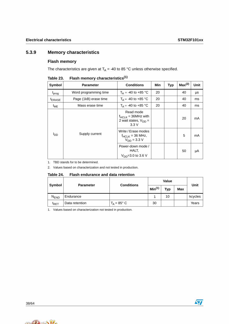
5.3.9 Memory characteristics
Flash memory
The characteristics are given at TA = −40 to 85 °C unless otherwise specified.
Table 24. Flash endurance and data retention
Table 23. Flash memory characteristics(1)
1. TBD stands for to be determined.
Symbol Parameter Conditions Min Typ Max(2)
2. Values based on characterization and not tested in production.
Unit
tprog Word programming time TA = −40 to +85 °C 20 40 µs
tERASE Page (1kB) erase time TA = −40 to +85 °C 20 40 ms
tME Mass erase time TA = −40 to +85 °C 20 40 ms
IDD Supply current
Read modefHCLK = 36MHz with 2 wait states, VDD =
3.3 V
20 mA
Write / Erase modes fHCLK = 36 MHz,
VDD = 3.3 V5 mA
Power-down mode / HALT,
VDD=3.0 to 3.6 V50 µA
Symbol Parameter ConditionsValue
UnitMin(1)
1. Values based on characterization not tested in production.
Typ Max
NEND Endurance 1 10 kcycles
tRET Data retention TA = 85° C 30 Years
STM32F101xx Electrical characteristics
39/64
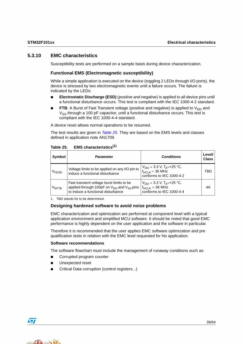
5.3.10 EMC characteristics
Susceptibility tests are performed on a sample basis during device characterization.
Functional EMS (Electromagnetic susceptibility)
While a simple application is executed on the device (toggling 2 LEDs through I/O ports). the device is stressed by two electromagnetic events until a failure occurs. The failure is indicated by the LEDs:
Electrostatic Discharge (ESD) (positive and negative) is applied to all device pins until a functional disturbance occurs. This test is compliant with the IEC 1000-4-2 standard.
FTB: A Burst of Fast Transient voltage (positive and negative) is applied to VDD and VSS through a 100 pF capacitor, until a functional disturbance occurs. This test is compliant with the IEC 1000-4-4 standard.
A device reset allows normal operations to be resumed.
The test results are given in Table 25. They are based on the EMS levels and classes defined in application note AN1709.
Designing hardened software to avoid noise problems
EMC characterization and optimization are performed at component level with a typical application environment and simplified MCU software. It should be noted that good EMC performance is highly dependent on the user application and the software in particular.
Therefore it is recommended that the user applies EMC software optimization and pre qualification tests in relation with the EMC level requested for his application.
Software recommendations
The software flowchart must include the management of runaway conditions such as:
Corrupted program counter
Unexpected reset
Critical Data corruption (control registers...)
Table 25. EMS characteristics(1)
1. TBD stands for to be determined.
Symbol Parameter ConditionsLevel/Class
VFESDVoltage limits to be applied on any I/O pin to induce a functional disturbance
VDD = 3.3 V, TA=+25 °C, fHCLK = 36 MHzconforms to IEC 1000-4-2
TBD
VEFTB
Fast transient voltage burst limits to be applied through 100pF on VDD and VSS pins to induce a functional disturbance
VDD = 3.3 V, TA=+25 °C, fHCLK = 36 MHzconforms to IEC 1000-4-4
4A
Electrical characteristics STM32F101xx
40/64
Prequalification trials
Most of the common failures (unexpected reset and program counter corruption) can be reproduced by manually forcing a low state on the NRST pin or the Oscillator pins for 1 second. To complete these trials, ESD stress can be applied directly on the device, over the range of specification values. When unexpected behavior is detected, the software can be hardened to prevent unrecoverable errors occurring (see application note AN1015).
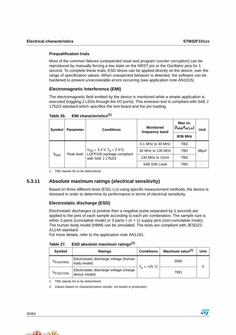
Electromagnetic Interference (EMI)
The electromagnetic field emitted by the device is monitored while a simple application is executed (toggling 2 LEDs through the I/O ports). This emission test is compliant with SAE J 1752/3 standard which specifies the test board and the pin loading.
5.3.11 Absolute maximum ratings (electrical sensitivity)
Based on three different tests (ESD, LU) using specific measurement methods, the device is stressed in order to determine its performance in terms of electrical sensitivity.
Electrostatic discharge (ESD)
Electrostatic discharges (a positive then a negative pulse separated by 1 second) are applied to the pins of each sample according to each pin combination. The sample size is either 3 parts (cumulative mode) or 3 parts × (n + 1) supply pins (non-cumulative mode).The human body model (HBM) can be simulated. The tests are compliant with JESD22-A114A standard.For more details, refer to the application note AN1181.
Table 26. EMI characteristics(1)
1. TBD stands for to be determined.
Symbol Parameter ConditionsMonitored
frequency band
Max vs. [fHSE/fHCLK]
Unit
8/36 MHz
SEMI Peak levelVDD = 3.3 V, TA = 2 5°C, LQFP100 package compliant with SAE J 1752/3
0.1 MHz to 30 MHz TBD
dBµV30 MHz to 130 MHz TBD
130 MHz to 1GHz TBD
SAE EMI Level TBD -
Table 27. ESD absolute maximum ratings(1)
1. TBD stands for to be determined.
Symbol Ratings Conditions Maximum value(2)
2. Values based on characterization results, not tested in production.
Unit
VESD(HBM)Electrostatic discharge voltage (human body model)
TA = +25 °C
2000
V
VESD(CDM)Electrostatic discharge voltage (charge device model)
TBD
STM32F101xx Electrical characteristics
41/64
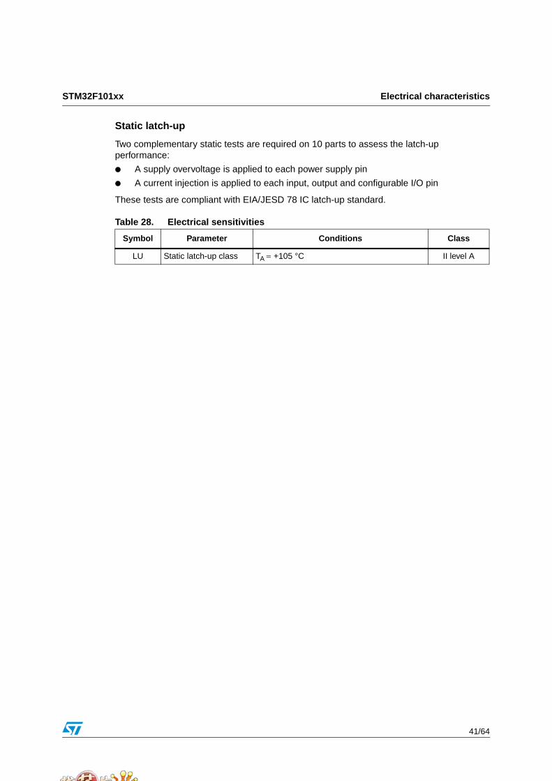
Static latch-up
Two complementary static tests are required on 10 parts to assess the latch-up performance:
A supply overvoltage is applied to each power supply pin
A current injection is applied to each input, output and configurable I/O pin
These tests are compliant with EIA/JESD 78 IC latch-up standard.
Table 28. Electrical sensitivities
Symbol Parameter Conditions Class
LU Static latch-up class TA = +105 °C II level A
Electrical characteristics STM32F101xx
42/64
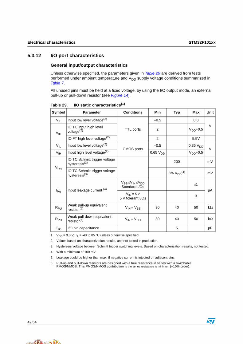
5.3.12 I/O port characteristics
General input/output characteristics
Unless otherwise specified, the parameters given in Table 29 are derived from tests performed under ambient temperature and VDD supply voltage conditions summarized in Table 7.
All unused pins must be held at a fixed voltage, by using the I/O output mode, an external pull-up or pull-down resistor (see Figure 14).
Table 29. I/O static characteristics(1)
1. VDD = 3.3 V, TA = −40 to 85 °C unless otherwise specified.
Symbol Parameter Conditions Min Typ Max Unit
VIL Input low level voltage(2)
2. Values based on characterization results, and not tested in production.
TTL ports
–0.5 0.8
V
VIH
IO TC input high level voltage(2) 2 VDD+0.5
IO FT high level voltage(2) 2 5.5V
VIL Input low level voltage(2)
CMOS ports–0.5 0.35 VDD
VVIH Input high level voltage(2) 0.65 VDD VDD+0.5
Vhys
IO TC Schmitt trigger voltage hysteresis(3)
3. Hysteresis voltage between Schmitt trigger switching levels. Based on characterization results, not tested.
200 mV
IO TC Schmitt trigger voltage hysteresis(3) 5% VDD
(4) mV
Ilkg Input leakage current (4)
4. With a minimum of 100 mV.
VSS ≤VIN ≤VDDStandard I/Os
±1µA
VIN = 5 V5 V tolerant I/Os
3
RPUWeak pull-up equivalent resistor(5)
5. Leakage could be higher than max. if negative current is injected on adjacent pins.
VIN = VSS 30 40 50 kΩ
RPDWeak pull-down equivalent resistor(6)
6. Pull-up and pull-down resistors are designed with a true resistance in series with a switchable PMOS/NMOS. This PMOS/NMOS contribution to the series resistance is minimum (~10% order).
VIN = VDD 30 40 50 kΩ
CIO I/O pin capacitance 5 pF

STM32F101xx Electrical characteristics
43/64
Figure 14. Unused I/O pin connection
Output driving current
The GPIOs (general purpose input/outputs) can sink or source up to +/-8 mA, and sink +20 mA (with a relaxed VOL).
In the user application, the number of I/O pins which can drive current must be limited to respect the absolute maximum rating specified in Section 5.2:
The sum of the currents sourced by all the I/Os on VDD, plus the maximum Run consumption of the MCU sourced on VDD, cannot exceed the absolute maximum rating IVDD (see Table 5).
The sum of the currents sunk by all the I/Os on VSS plus the maximum Run consumption of the MCU sunk on VSS cannot exceed the absolute maximum rating IVSS (see Table 5).
ai14130
10 kΩ
10 kΩ
UNUSED I/O PORT
STM32F101
VDD
UNUSED I/O PORT
STM32F101
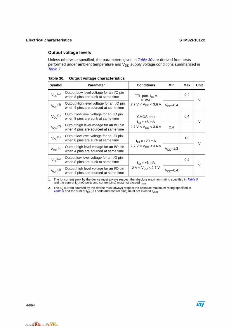
Electrical characteristics STM32F101xx
44/64
Output voltage levels
Unless otherwise specified, the parameters given in Table 30 are derived from tests performed under ambient temperature and VDD supply voltage conditions summarized in Table 7.
Table 30. Output voltage characteristics
Symbol Parameter Conditions Min Max Unit
VOL(1)
1. The IIO current sunk by the device must always respect the absolute maximum rating specified in Table 5 and the sum of IIO (I/O ports and control pins) must not exceed IVSS.
Output Low level voltage for an I/O pin when 8 pins are sunk at same time TTL port, IIO =
+8 mA,2.7 V < VDD < 3.6 V
0.4
V
VOH(2)
2. The IIO current sourced by the device must always respect the absolute maximum rating specified in Table 5 and the sum of IIO (I/O ports and control pins) must not exceed IVDD.
Output High level voltage for an I/O pin when 4 pins are sourced at same time
VDD–0.4
VOL(1) Output low level voltage for an I/O pin
when 8 pins are sunk at same time CMOS portIIO = +8 mA
2.7 V < VDD < 3.6 V
0.4
V
VOH(2) Output high level voltage for an I/O pin
when 4 pins are sourced at same time2.4
VOL(1) Output low level voltage for an I/O pin
when 8 pins are sunk at same time IIO = +20 mA2.7 V < VDD < 3.6 V
1.3
V
VOH (2) Output high level voltage for an I/O pin
when 4 pins are sourced at same time VDD–1.3
VOL(1) Output low level voltage for an I/O pin
when 8 pins are sunk at same time IIO = +6 mA
2 V < VDD < 2.7 V
0.4
V
VOH(2) Output high level voltage for an I/O pin
when 4 pins are sourced at same time VDD–0.4
STM32F101xx Electrical characteristics
45/64
Input/output AC characteristics
The definition and values of input/output AC characteristics are given in Figure 15 and Table 31, respectively.
Unless otherwise specified, the parameters given in Table 31 are derived from tests performed under ambient temperature and VDD supply voltage conditions summarized in Table 7.
Table 31. I/O AC characteristics(1)
1. Refer to the Reference user manual UM0306 for a description of GPIO Port configuration register.
I/O mode(1) Symbol Parameter Conditions Max Unit
10
fmax(IO)out Maximum frequency(2)
2. The maximum frequency is defined in Figure 15.
CL = 50 pF, VDD = 2 V to 3.6 V 2 MHz
tf(IO)outOutput high to low level fall time(3)
3. Values based on design simulation and validated on silicon, not tested in production.
CL = 50 pF, VDD = 2 V to 3.6 V
125
ns
tr(IO)outOutput low to high level rise time(3) 125
01
fmax(IO)out Maximum frequency(2) CL= 50 pF, VDD = 2 V to 3.6 V 10 MHz
tf(IO)outOutput high to low level fall time(3)
CL= 50 pF, VDD = 2 V to 3.6 V
25
ns
tr(IO)outOutput low to high level rise time(3) 25
11
Fmax(IO)out Maximum Frequency(2)
CL= 30 pF, VDD = 2.7 V to 3.6 V 50 MHz
CL = 50 pF, VDD = 2.7 V to 3.6 V 30 MHz
CL = 50 pF, VDD = 2 V to 2.7 V 20 MHz
tf(IO)outOutput high to low level fall time(3)
CL = 30 pF, VDD = 2.7 V to 3.6 V 5
ns
CL = 50 pF, VDD = 2.7 V to 3.6 V 8
CL = 50 pF, VDD = 2 V to 2.7 V 12
tr(IO)outOutput low to high level rise time(3)
CL = 30 pF, VDD = 2.7 V to 3.6 V 5
CL = 50 pF, VDD = 2.7 V to 3.6 V 8
CL = 50 pF, VDD = 2 V to 2.7 V 12
- tEXTIpwPulse width of external signals detected by the EXTI controller
10 ns
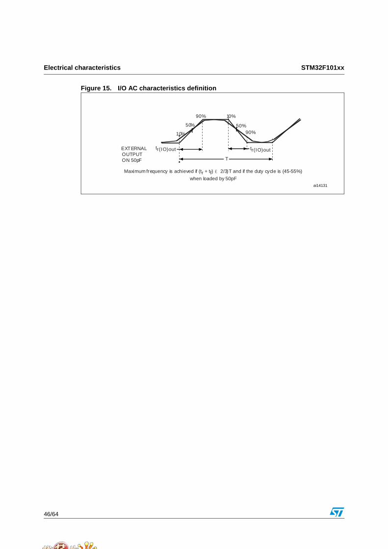
Electrical characteristics STM32F101xx
46/64
Figure 15. I/O AC characteristics definition
ai14131
10%
90%
50%
tr(IO)outOUTPUTEXTERNAL
ON 50pF
Maximum frequency is achieved if (tr + tf) £ 2/3)T and if the duty cycle is (45-55%)
10%
50%90%
when loaded by 50pF
T
tr(IO)out
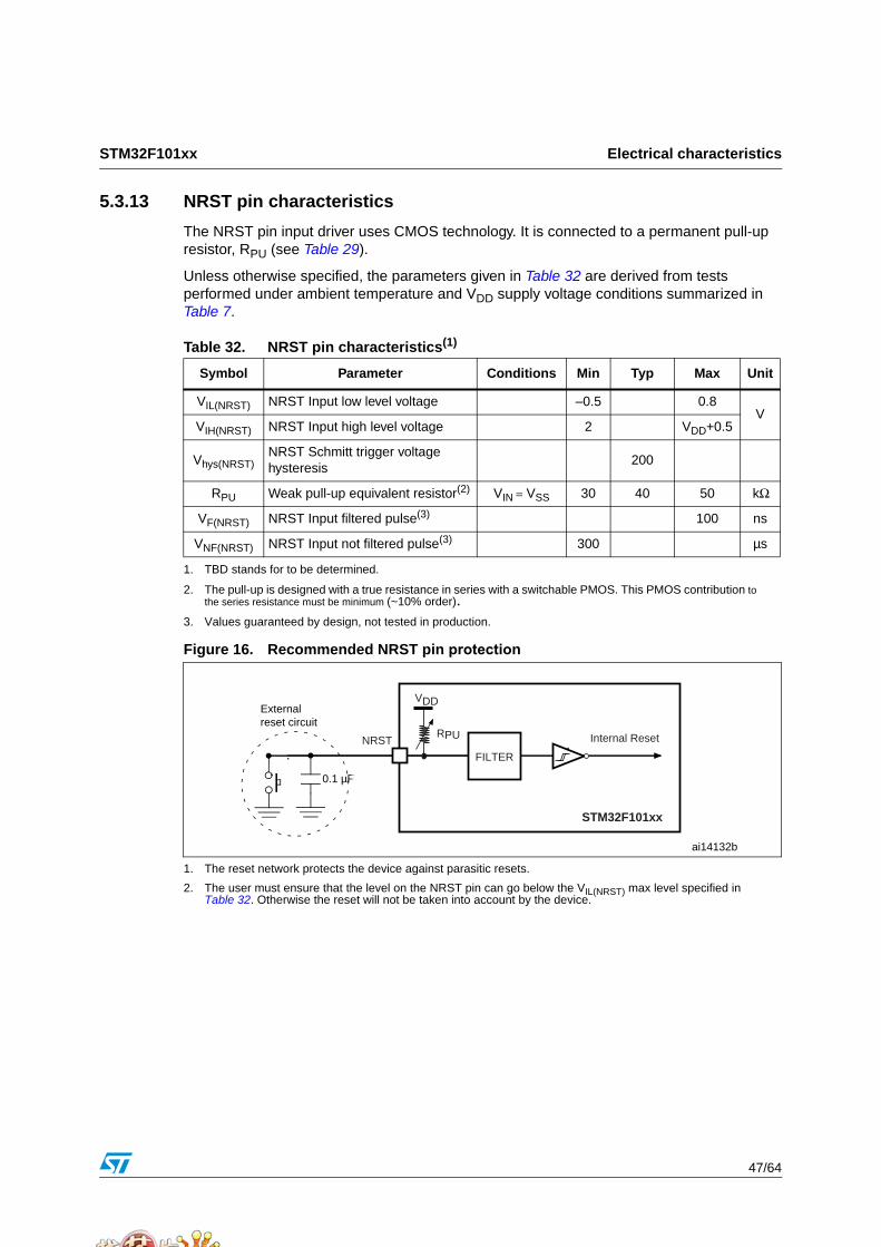
STM32F101xx Electrical characteristics
47/64
5.3.13 NRST pin characteristics
The NRST pin input driver uses CMOS technology. It is connected to a permanent pull-up resistor, RPU (see Table 29).
Unless otherwise specified, the parameters given in Table 32 are derived from tests performed under ambient temperature and VDD supply voltage conditions summarized in Table 7.
Figure 16. Recommended NRST pin protection
1. The reset network protects the device against parasitic resets.
2. The user must ensure that the level on the NRST pin can go below the VIL(NRST) max level specified in Table 32. Otherwise the reset will not be taken into account by the device.
Table 32. NRST pin characteristics(1)
1. TBD stands for to be determined.
Symbol Parameter Conditions Min Typ Max Unit
VIL(NRST) NRST Input low level voltage –0.5 0.8V
VIH(NRST) NRST Input high level voltage 2 VDD+0.5
Vhys(NRST)NRST Schmitt trigger voltage hysteresis
200
RPU Weak pull-up equivalent resistor(2)
2. The pull-up is designed with a true resistance in series with a switchable PMOS. This PMOS contribution to the series resistance must be minimum (~10% order).
VIN = VSS 30 40 50 kΩ
VF(NRST) NRST Input filtered pulse(3)
3. Values guaranteed by design, not tested in production.
100 ns
VNF(NRST) NRST Input not filtered pulse(3) 300 µs
ai14132b
STM32F101xx
RPUNRST
VDD
FILTER
Internal Reset
0.1 µF
Externalreset circuit
Electrical characteristics STM32F101xx
48/64
5.3.14 TIM timer characteristics
Unless otherwise specified, the parameters given in Table 33 are derived from tests performed under ambient temperature, fPCLKx frequency and VDD supply voltage conditions summarized in Table 7.
Refer to Section 5.3.12: I/O port characteristics for details on the input/output alternate function characteristics (output compare, input capture, external clock, PWM output).
Table 33. TIMx characteristics
Symbol Parameter TIMx(1)
1. x gives the TIM concerned; where x = 2, TIM2 is concerned, etc.
Conditions Min Max Unit
tres(TIM)Timer resolution time
x = 2, 3, 41 tTIMxCLK
fTIMxCLK = 36 MHz 27.8 ns
fEXT
Timer external clock frequency on CH1 to CH4
x = 2, 3, 4 0 fTIMxCLK/2 MHz
fTIMxCLK = 36 MHz 0 18 MHz
ResTIM Timer resolution 16 bit
tCOUNTER
16-bit counter clock period when internal clock is selected
x = 2, 3, 41 65536 tTIMxCLK
fTIMxCLK = 36 MHz 0.0278 1820 µs
tMAX_COUNTMaximum possible count
x = 2, 3, 4
65536 × 65536
tTIMxCLK
fTIMxCLK = 36 MHz 119.2 s
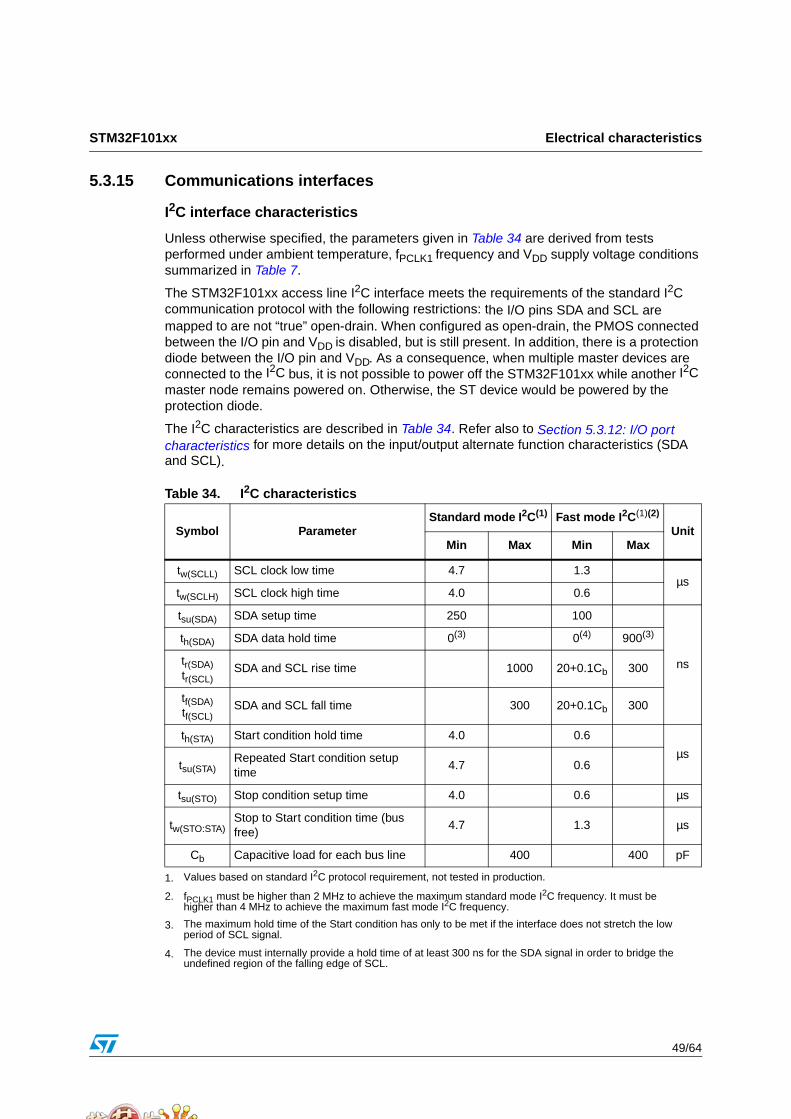
STM32F101xx Electrical characteristics
49/64
5.3.15 Communications interfaces
I2C interface characteristics
Unless otherwise specified, the parameters given in Table 34 are derived from tests performed under ambient temperature, fPCLK1 frequency and VDD supply voltage conditions summarized in Table 7.
The STM32F101xx access line I2C interface meets the requirements of the standard I2C communication protocol with the following restrictions: the I/O pins SDA and SCL are mapped to are not “true” open-drain. When configured as open-drain, the PMOS connected between the I/O pin and VDD is disabled, but is still present. In addition, there is a protection diode between the I/O pin and VDD. As a consequence, when multiple master devices are connected to the I2C bus, it is not possible to power off the STM32F101xx while another I2C master node remains powered on. Otherwise, the ST device would be powered by the protection diode.
The I2C characteristics are described in Table 34. Refer also to Section 5.3.12: I/O port characteristics for more details on the input/output alternate function characteristics (SDA and SCL).
Table 34. I2C characteristics
Symbol ParameterStandard mode I2C(1)
1. Values based on standard I2C protocol requirement, not tested in production.
Fast mode I2C(1)(2)
2. fPCLK1 must be higher than 2 MHz to achieve the maximum standard mode I2C frequency. It must be higher than 4 MHz to achieve the maximum fast mode I2C frequency.
UnitMin Max Min Max
tw(SCLL) SCL clock low time 4.7 1.3 µs
tw(SCLH) SCL clock high time 4.0 0.6
tsu(SDA) SDA setup time 250 100
ns
th(SDA) SDA data hold time 0(3)
3. The maximum hold time of the Start condition has only to be met if the interface does not stretch the low period of SCL signal.
0(4)
4. The device must internally provide a hold time of at least 300 ns for the SDA signal in order to bridge the undefined region of the falling edge of SCL.
900(3)
tr(SDA)tr(SCL)
SDA and SCL rise time 1000 20+0.1Cb 300
tf(SDA)tf(SCL)
SDA and SCL fall time 300 20+0.1Cb 300
th(STA) Start condition hold time 4.0 0.6
µstsu(STA)
Repeated Start condition setup time
4.7 0.6
tsu(STO) Stop condition setup time 4.0 0.6 µs
tw(STO:STA)Stop to Start condition time (bus free)
4.7 1.3 µs
Cb Capacitive load for each bus line 400 400 pF
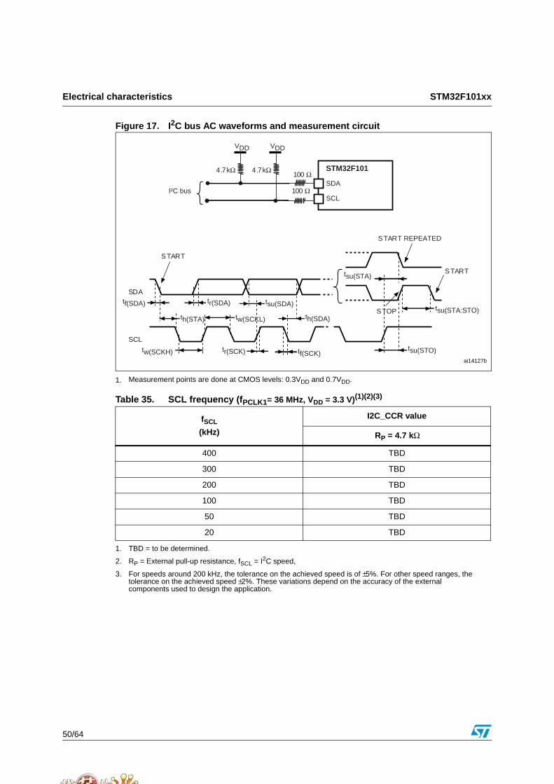
Electrical characteristics STM32F101xx
50/64
Figure 17. I2C bus AC waveforms and measurement circuit
1. Measurement points are done at CMOS levels: 0.3VDD and 0.7VDD.
Table 35. SCL frequency (fPCLK1= 36 MHz, VDD = 3.3 V)(1)(2)(3)
1. TBD = to be determined.
2. RP = External pull-up resistance, fSCL = I2C speed,
3. For speeds around 200 kHz, the tolerance on the achieved speed is of ±5%. For other speed ranges, the tolerance on the achieved speed ±2%. These variations depend on the accuracy of the external components used to design the application.
fSCL
(kHz)
I2C_CCR value
RP = 4.7 kΩ
400 TBD
300 TBD
200 TBD
100 TBD
50 TBD
20 TBD
ai14127b
START
SDA
100 Ω4.7kΩ
I²C bus
4.7kΩ
100 Ω
VDDVDD
STM32F101
SDA
SCL
tf(SDA) tr(SDA)
SCL
th(STA)
tw(SCKH)
tw(SCKL)
tsu(SDA)
tr(SCK) tf(SCK)
th(SDA)
START REPEATED
STARTtsu(STA)
tsu(STO)
STOP tsu(STA:STO)

STM32F101xx Electrical characteristics
51/64
SPI interface characteristics
Unless otherwise specified, the parameters given in Table 36 are derived from tests performed under ambient temperature, fPCLKx frequency and VDD supply voltage conditions summarized in Table 7.
Refer to Section 5.3.12: I/O port characteristics for more details on the input/output alternate function characteristics (NSS, SCK, MOSI, MISO).
Table 36. SPI characteristics(1)
1. TBD = to be determined.
Symbol Parameter Conditions Min Max Unit
fSCK1/tc(SCK)
SPI clock frequencyMaster mode TBD TBD
MHzSlave mode 0 TBD
tr(SCK)tf(SCK)
SPI clock rise and fall time Capacitive load: C = 50 pF TBD
ns
tsu(NSS)(2)
2. Values based on design simulation and/or characterization results, and not tested in production.
NSS setup time Slave mode 0
th(NSS)(2) NSS hold time Slave mode 0
tw(SCKH)(2)
tw(SCKL)(2) SCK high and low time
Master mode, fPCLK = TBD, presc = TBD
TBD
tsu(MI) (2)
tsu(SI)(2) Data input setup time
Master mode TBD
Slave mode TBD
th(MI) (2)
th(SI)(2) Data input hold time
Master mode TBD
Slave mode TBD
Master mode, fPCLK = TBD TBD(3)
3. Depends on fPCLK. For example, if fPCLK= 8 MHz, then tPCLK = 1/fPLCLK =125 ns and tv(MO) = 255 ns.
Slave mode, fPCLK = TBD TBD(3)
ta(SO)(2)(4)
4. Min time is for the minimum time to drive the output and the max time is for the maximum time to validate the data.
Data output access timeSlave mode TBD TBD
Slave mode, fPCLK = TBD TBD TBD
tdis(SO)(2)(5)
5. Min time is for the minimum time to invalidate the output and the max time is for the maximum time to put the data in Hi-Z
Data output disable time Slave mode TBD TBD
tv(SO) (2)(1) Data output valid time
Slave mode (after enable edge) TBD
fPCLK = TBD TBD
tv(MO)(2)(1) Data output valid time
Master mode (after enable edge) TBD
fPCLK = TBD TBD TBD
th(SO)(2)
Data output hold timeSlave mode (after enable edge) TBD
th(MO)(2) Master mode (after enable edge) TBD
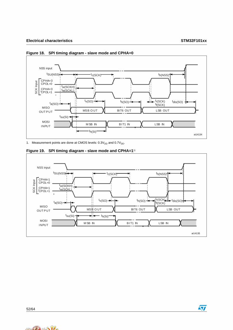
Electrical characteristics STM32F101xx
52/64
Figure 18. SPI timing diagram - slave mode and CPHA=0
1. Measurement points are done at CMOS levels: 0.3VDD and 0.7VDD.
Figure 19. SPI timing diagram - slave mode and CPHA=11)
ai14134
SC
K In
put CPHA=0
MOSI
INPUT
MISOOUT PUT
CPHA=0
MSB O UT
M SB IN
BIT6 OUT
LSB IN
LSB OUT
CPOL=0
CPOL=1
BIT1 IN
NSS input
tSU(NSS) tc(SCK) th(NSS)
ta(SO)
tw(SCKH)tw(SCKL)
tv(SO) th(SO) tr(SCK)tf(SCK)
tdis(SO)
tsu(SI)
th(SI)
ai14135
SC
K In
put CPHA=1
MOSI
INPUT
MISOOUT PUT
CPHA=1
MSB O UT
M SB IN
BIT6 OUT
LSB IN
LSB OUT
CPOL=0
CPOL=1
BIT1 IN
tSU(NSS) tc(SCK) th(NSS)
ta(SO)
tw(SCKH)tw(SCKL)
tv(SO) th(SO)tr(SCK)tf(SCK)
tdis(SO)
tsu(SI) th(SI)
NSS input
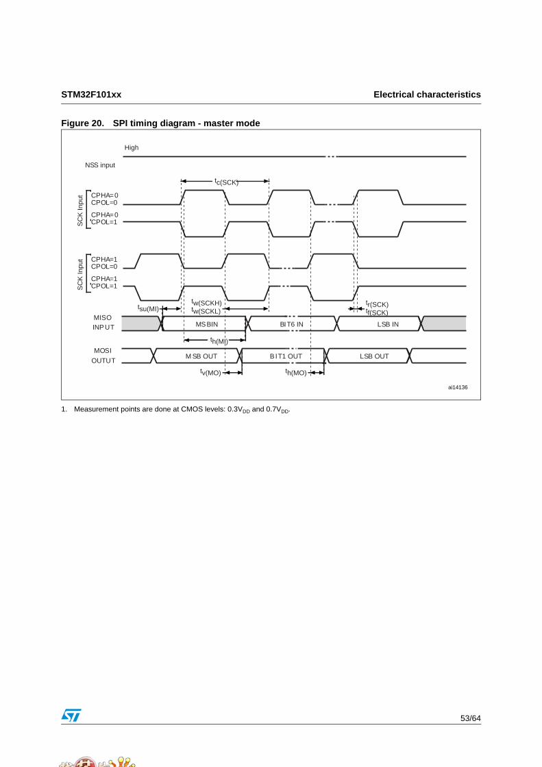
STM32F101xx Electrical characteristics
53/64
Figure 20. SPI timing diagram - master mode
1. Measurement points are done at CMOS levels: 0.3VDD and 0.7VDD.
ai14136
SC
K In
put CPHA=0
MOSI
OUTUT
MISOINPUT
CPHA=0
MSBIN
M SB OUT
BIT6 IN
LSB OUT
LSB IN
CPOL=0
CPOL=1
BIT1 OUT
NSS input
tc(SCK)
tw(SCKH)tw(SCKL)
tr(SCK)tf(SCK)
th(MI)
High
SC
K In
put CPHA=1
CPHA=1
CPOL=0
CPOL=1
tsu(MI)
tv(MO) th(MO)
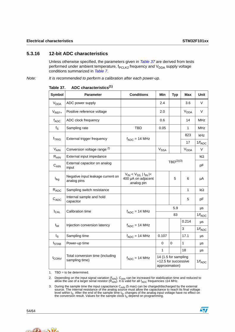
Electrical characteristics STM32F101xx
54/64
5.3.16 12-bit ADC characteristics
Unless otherwise specified, the parameters given in Table 37 are derived from tests performed under ambient temperature, fPCLK2 frequency and VDDA supply voltage conditions summarized in Table 7.
Note: It is recommended to perform a calibration after each power-up.
Table 37. ADC characteristics(1)
1. TBD = to be determined.
Symbol Parameter Conditions Min Typ Max Unit
VDDA ADC power supply 2.4 3.6 V
VREF+ Positive reference voltage 2.0 VDDA V
fADC ADC clock frequency 0.6 14 MHz
fS Sampling rate TBD 0.05 1 MHz
fTRIG External trigger frequency fADC = 14 MHz823 kHz
17 1/fADC
VAIN Conversion voltage range 2) VSSA VDDA V
RAIN External input impedance
TBD(2)(3)
2. Depending on the input signal variation (fAIN), CAIN can be increased for stabilization time and reduced to allow the use of a larger serial resistor (RAIN). It is valid for all fADC frequencies ≤ 14 MHz.
3. During the sample time the input capacitance CAIN (5 max) can be charged/discharged by the external source. The internal resistance of the analog source must allow the capacitance to reach its final voltage level within tS. After the end of the sample time tS, changes of the analog input voltage have no effect on the conversion result. Values for the sample clock tS depend on programming.
kΩ
CAINExternal capacitor on analog input
pF
IlkgNegative input leakage current on analog pins
VIN < VSS, | IIN |< 400 µA on adjacent
analog pin5 6 µA
RADC Sampling switch resistance 1 kΩ
CADCInternal sample and hold capacitor
5 pF
tCAL Calibration time fADC = 14 MHz5.9 µs
83 1/fADC
tlat Injection conversion latency fADC = 14 MHz0.214 µs
3 1/fADC
tS Sampling time fADC = 14 MHz 0.107 17.1 µs
tSTAB Power-up time 0 0 1 µs
tCONVTotal conversion time (including sampling time)
fADC = 14 MHz
1 18 µs
14 (1.5 for sampling +12.5 for successive approximation)
1/fADC
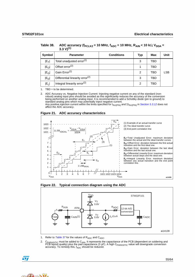
STM32F101xx Electrical characteristics
55/64
Figure 21. ADC accuracy characteristics
Figure 22. Typical connection diagram using the ADC
1. Refer to Table 37 for the values of RADC and CADC.
2. CPARASITIC must be added to CAIN. It represents the capacitance of the PCB (dependent on soldering and PCB layout quality) plus the pad capacitance (3 pF). A high CPARASITIC value will downgrade conversion accuracy. To remedy this, fADC should be reduced.
Table 38. ADC accuracy (fPCLK2 = 10 MHz, fADC = 10 MHz, RAIN < 10 kΩ, VDDA = 3.3 V)(1)
1. TBD = to be determined.
Symbol Parameter Conditions Typ Max Unit
|ET| Total unadjusted error(2)
2. ADC Accuracy vs. Negative Injection Current: Injecting negative current on any of the standard (non-robust) analog input pins should be avoided as this significantly reduces the accuracy of the conversion being performed on another analog input. It is recommended to add a Schottky diode (pin to ground) to standard analog pins which may potentially inject negative current. Any positive injection current within the limits specified for IINJ(PIN) and ΣIINJ(PIN) in Section 5.3.12 does not affect the ADC accuracy.
3 TBD
LSB
|EO| Offset error(2) 1 TBD
|EG| Gain Error(2) 2 TBD
|ED| Differential linearity error(2) 3 TBD
|EL| Integral linearity error(2) 2 TBD
EO
EG
1 LSBIDEAL
1LSBIDEAL
VDDA VSSA–
1024-----------------------------------------=
(1) Example of an actual transfer curve(2) The ideal transfer curve(3) End point correlation line
ET=Total Unadjusted Error: maximum deviationbetween the actual and the ideal transfer curves.EO=Offset Error: deviation between the first actualtransition and the first ideal one.EG=Gain Error: deviation between the last idealtransition and the last actual one.ED=Differential Linearity Error: maximum deviationbetween actual steps and the ideal one.EL=Integral Linearity Error: maximum deviationbetween any actual transition and the end pointcorrelation line.
1023
1022
1021
5
4
3
2
1
0
7
6
1 2 3 4 5 6 7 1021 1022 1023 1024
(1)
(2)
ET
ED
EL
(3)
VDDAVSSA ai14395
ai14139
STM32F101VDD
AINx
IL±1mA0.6VVT
RAIN
CAIN(1)VAIN
0.6VVT
RADC 12-bit A/Dconversion
CADC
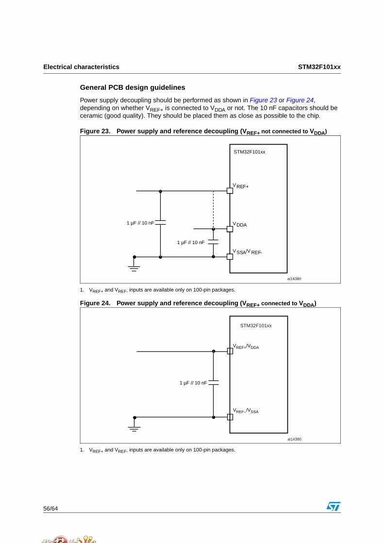
Electrical characteristics STM32F101xx
56/64
General PCB design guidelines
Power supply decoupling should be performed as shown in Figure 23 or Figure 24, depending on whether VREF+ is connected to VDDA or not. The 10 nF capacitors should be ceramic (good quality). They should be placed them as close as possible to the chip.
Figure 23. Power supply and reference decoupling (VREF+ not connected to VDDA)
1. VREF+ and VREF- inputs are available only on 100-pin packages.
Figure 24. Power supply and reference decoupling (VREF+ connected to VDDA)
1. VREF+ and VREF- inputs are available only on 100-pin packages.
VREF+
STM32F101xx
VDDA
VSSA/V REF-
1 µF // 10 nF
1 µF // 10 nF
ai14380
VREF+/VDDA
STM32F101xx
1 µF // 10 nF
VREF–/VSSA
ai14380
STM32F101xx Electrical characteristics
57/64
5.3.17 Temperature sensor characteristics
Table 39. TS characteristics
Symbol Parameter Conditions Min Typ Max Unit
TL VSENSE linearity with temperature ±1.5 °C
Avg_Slope Average slope 4.478 mV/°C
V25 Voltage at 25°C 1.4 V
tSTART Startup time 4 10 µs
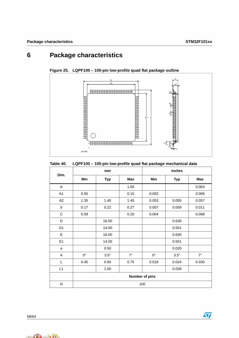
Package characteristics STM32F101xx
58/64
6 Package characteristics
Figure 25. LQPF100 – 100-pin low-profile quad flat package outline
Table 40. LQPF100 – 100-pin low-profile quad flat package mechanical data
Dim.mm inches
Min Typ Max Min Typ Max
A 1.60 0.063
A1 0.05 0.15 0.002 0.006
A2 1.35 1.40 1.45 0.053 0.055 0.057
b 0.17 0.22 0.27 0.007 0.009 0.011
C 0.09 0.20 0.004 0.008
D 16.00 0.630
D1 14.00 0.551
E 16.00 0.630
E1 14.00 0.551
e 0.50 0.020
θ 0° 3.5° 7° 0° 3.5° 7°
L 0.45 0.60 0.75 0.018 0.024 0.030
L1 1.00 0.039
Number of pins
N 100
h
c
L
L1
e
b
A
A2
A1
D
D1
EE1
ai14382
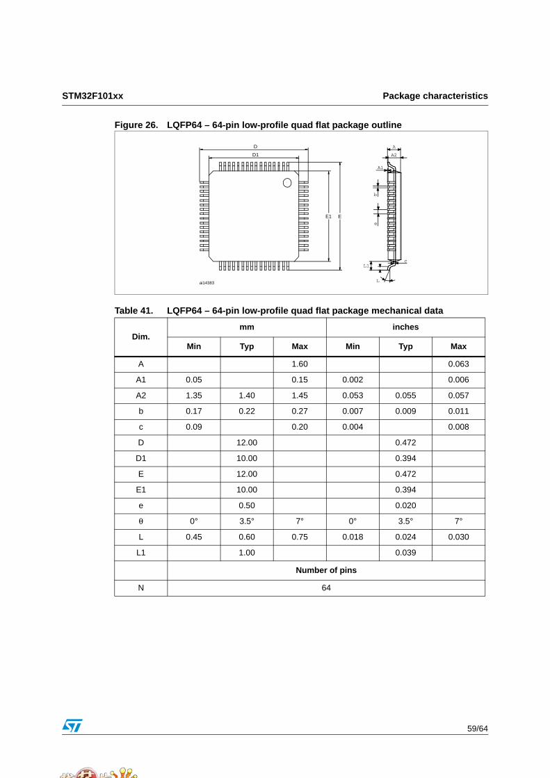
STM32F101xx Package characteristics
59/64
Figure 26. LQFP64 – 64-pin low-profile quad flat package outline
Table 41. LQFP64 – 64-pin low-profile quad flat package mechanical data
Dim.mm inches
Min Typ Max Min Typ Max
A 1.60 0.063
A1 0.05 0.15 0.002 0.006
A2 1.35 1.40 1.45 0.053 0.055 0.057
b 0.17 0.22 0.27 0.007 0.009 0.011
c 0.09 0.20 0.004 0.008
D 12.00 0.472
D1 10.00 0.394
E 12.00 0.472
E1 10.00 0.394
e 0.50 0.020
θ 0° 3.5° 7° 0° 3.5° 7°
L 0.45 0.60 0.75 0.018 0.024 0.030
L1 1.00 0.039
Number of pins
N 64
A
A2
A1
cL1
L
EE1
D
D1
e
b
ai14383
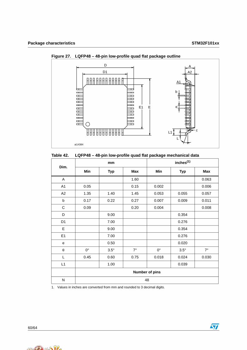
Package characteristics STM32F101xx
60/64
Figure 27. LQFP48 – 48-pin low-profile quad flat package outline
Table 42. LQFP48 – 48-pin low-profile quad flat package mechanical data
Dim.mm inches(1)
1. Values in inches are converted from mm and rounded to 3 decimal digits.
Min Typ Max Min Typ Max
A 1.60 0.063
A1 0.05 0.15 0.002 0.006
A2 1.35 1.40 1.45 0.053 0.055 0.057
b 0.17 0.22 0.27 0.007 0.009 0.011
C 0.09 0.20 0.004 0.008
D 9.00 0.354
D1 7.00 0.276
E 9.00 0.354
E1 7.00 0.276
e 0.50 0.020
θ 0° 3.5° 7° 0° 3.5° 7°
L 0.45 0.60 0.75 0.018 0.024 0.030
L1 1.00 0.039
Number of pins
N 48
EE1
D
D1
L1
L
c
e
b
A1
A2
A
ai14384
STM32F101xx Package characteristics
61/64
6.1 Thermal characteristicsThe average chip-junction temperature, TJ, in degrees Celsius, may be calculated using the following equation:
TJ = TA + (PD x ΘJA) (1)
Where:
TA is the ambient temperature in ° C,
ΘJA is the package junction-to-ambient thermal resistance, in ° C/W,
PD is the sum of PINT and PI/O (PD = PINT + PI/O),
PINT is the product of IDD and VDD, expressed in Watts. This is the chip internal power.
PI/O represents the power dissipation on input and output pins;
Most of the time for the application PI/O< PINT and can be neglected. On the other hand, PI/O may be significant if the device is configured to drive continuously external modules and/or memories.
An approximate relationship between PD and TJ (if PI/O is neglected) is given by:
PD = K / (TJ + 273 °C) (2)
Therefore (solving equations 1 and 2):
K = PD x (TA + 273 °C) + ΘJA x PD2 (3)
where:
K is a constant for the particular part, which may be determined from equation (3) by measuring PD (at equilibrium) for a known TA. Using this value of K, the values of PD and TJ may be obtained by solving equations (1) and (2) iteratively for any value of TA.
Table 43. Thermal characteristics
Symbol Parameter Value Unit
ΘJA
Thermal resistance junction-ambientLQFP 100 - 14 x 14 mm / 0.5 mm pitch
46
°C/WThermal resistance junction-ambientLQFP 64 - 10 x 10 mm / 0.5 mm pitch
45
Thermal resistance junction-ambientLQFP 48 - 7 x 7 mm / 0.5 mm pitch
55
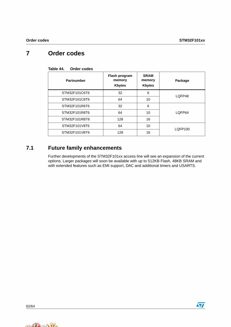
Order codes STM32F101xx
62/64
7 Order codes
7.1 Future family enhancementsFurther developments of the STM32F101xx access line will see an expansion of the current options. Larger packages will soon be available with up to 512KB Flash, 48KB SRAM and with extended features such as EMI support, DAC and additional timers and USARTS.
Table 44. Order codes
PartnumberFlash program
memory
Kbytes
SRAM memory
KbytesPackage
STM32F101C6T6 32 6LQFP48
STM32F101C8T6 64 10
STM32F101R6T6 32 6
LQFP64STM32F101R8T6 64 10
STM32F101RBT6 128 16
STM32F101V8T6 64 10LQFP100
STM32F101VBT6 128 16
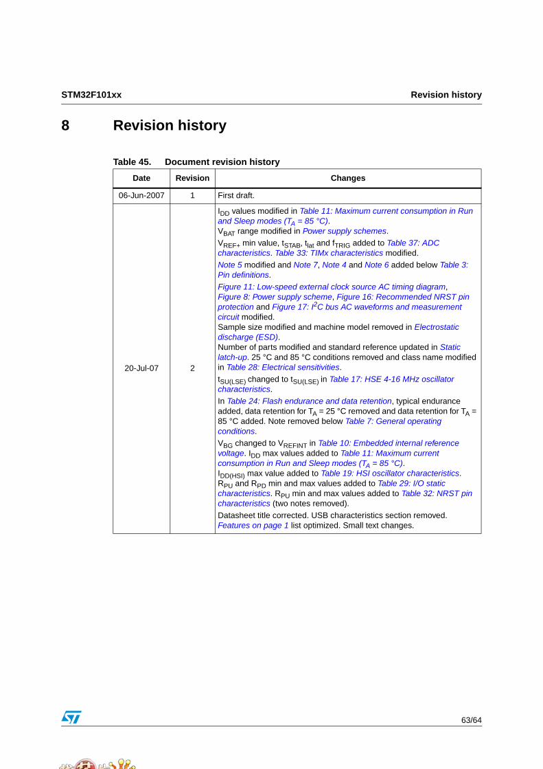
STM32F101xx Revision history
63/64
8 Revision history
Table 45. Document revision history
Date Revision Changes
06-Jun-2007 1 First draft.
20-Jul-07 2
IDD values modified in Table 11: Maximum current consumption in Run and Sleep modes (TA = 85 °C).VBAT range modified in Power supply schemes.
VREF+ min value, tSTAB, tlat and fTRIG added to Table 37: ADC characteristics. Table 33: TIMx characteristics modified.
Note 5 modified and Note 7, Note 4 and Note 6 added below Table 3: Pin definitions.
Figure 11: Low-speed external clock source AC timing diagram, Figure 8: Power supply scheme, Figure 16: Recommended NRST pin protection and Figure 17: I2C bus AC waveforms and measurement circuit modified.Sample size modified and machine model removed in Electrostatic discharge (ESD).Number of parts modified and standard reference updated in Static latch-up. 25 °C and 85 °C conditions removed and class name modified in Table 28: Electrical sensitivities.
tSU(LSE) changed to tSU(LSE) in Table 17: HSE 4-16 MHz oscillator characteristics.
In Table 24: Flash endurance and data retention, typical endurance added, data retention for TA = 25 °C removed and data retention for TA = 85 °C added. Note removed below Table 7: General operating conditions.VBG changed to VREFINT in Table 10: Embedded internal reference voltage. IDD max values added to Table 11: Maximum current consumption in Run and Sleep modes (TA = 85 °C).IDD(HSI) max value added to Table 19: HSI oscillator characteristics.RPU and RPD min and max values added to Table 29: I/O static characteristics. RPU min and max values added to Table 32: NRST pin characteristics (two notes removed).
Datasheet title corrected. USB characteristics section removed.Features on page 1 list optimized. Small text changes.
STM32F101xx
64/64
Please Read Carefully:
Information in this document is provided solely in connection with ST products. STMicroelectronics NV and its subsidiaries (“ST”) reserve theright to make changes, corrections, modifications or improvements, to this document, and the products and services described herein at anytime, without notice.
All ST products are sold pursuant to ST’s terms and conditions of sale.
Purchasers are solely responsible for the choice, selection and use of the ST products and services described herein, and ST assumes noliability whatsoever relating to the choice, selection or use of the ST products and services described herein.
No license, express or implied, by estoppel or otherwise, to any intellectual property rights is granted under this document. If any part of thisdocument refers to any third party products or services it shall not be deemed a license grant by ST for the use of such third party productsor services, or any intellectual property contained therein or considered as a warranty covering the use in any manner whatsoever of suchthird party products or services or any intellectual property contained therein.
UNLESS OTHERWISE SET FORTH IN ST’S TERMS AND CONDITIONS OF SALE ST DISCLAIMS ANY EXPRESS OR IMPLIEDWARRANTY WITH RESPECT TO THE USE AND/OR SALE OF ST PRODUCTS INCLUDING WITHOUT LIMITATION IMPLIEDWARRANTIES OF MERCHANTABILITY, FITNESS FOR A PARTICULAR PURPOSE (AND THEIR EQUIVALENTS UNDER THE LAWSOF ANY JURISDICTION), OR INFRINGEMENT OF ANY PATENT, COPYRIGHT OR OTHER INTELLECTUAL PROPERTY RIGHT.
UNLESS EXPRESSLY APPROVED IN WRITING BY AN AUTHORIZED ST REPRESENTATIVE, ST PRODUCTS ARE NOTRECOMMENDED, AUTHORIZED OR WARRANTED FOR USE IN MILITARY, AIR CRAFT, SPACE, LIFE SAVING, OR LIFE SUSTAININGAPPLICATIONS, NOR IN PRODUCTS OR SYSTEMS WHERE FAILURE OR MALFUNCTION MAY RESULT IN PERSONAL INJURY,DEATH, OR SEVERE PROPERTY OR ENVIRONMENTAL DAMAGE. ST PRODUCTS WHICH ARE NOT SPECIFIED AS "AUTOMOTIVEGRADE" MAY ONLY BE USED IN AUTOMOTIVE APPLICATIONS AT USER’S OWN RISK.
Resale of ST products with provisions different from the statements and/or technical features set forth in this document shall immediately voidany warranty granted by ST for the ST product or service described herein and shall not create or extend in any manner whatsoever, anyliability of ST.
ST and the ST logo are trademarks or registered trademarks of ST in various countries.
Information in this document supersedes and replaces all information previously supplied.
The ST logo is a registered trademark of STMicroelectronics. All other names are the property of their respective owners.
© 2007 STMicroelectronics - All rights reserved
STMicroelectronics group of companies
Australia - Belgium - Brazil - Canada - China - Czech Republic - Finland - France - Germany - Hong Kong - India - Israel - Italy - Japan - Malaysia - Malta - Morocco - Singapore - Spain - Sweden - Switzerland - United Kingdom - United States of America
www.st.com


![RRR工法協会[Association of RRR Construction System] - > 24m: 720 cm @ s g ù 01 01 ... · 2014. 5. 26. · 01 01>0 cit 01 04 ctt St o Ìõá B ctt s s E 94 01 sas 04k ží (9](https://img.pdfslide.tips/doc/110x75/60c1c181f991ab4bcb41c1b9/rrrassociation-of-rrr-construction-system-24m-720-cm-s-g.jpg)