Embed Size (px)
Citation preview
Arria II Device Handbook Volume 1: Device InterfacesDecember 2011
AIIGX51003-3.2
© 2011 Altera Corporation. All rights reserved. ALTERA, ARRand/or trademarks of Altera Corporation in the U.S. and otherwww.altera.com/common/legal.html. Altera warrants performreserves the right to make changes to any products and servicesinformation, product, or service described herein except as expspecifications before relying on any published information and
December 2011AIIGX51003-3.2
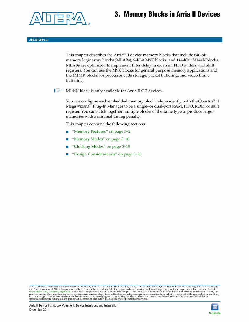
3. Memory Blocks in Arria II Devices
This chapter describes the Arria® II device memory blocks that include 640-bit memory logic array blocks (MLABs), 9-Kbit M9K blocks, and 144-Kbit M144K blocks. MLABs are optimized to implement filter delay lines, small FIFO buffers, and shift registers. You can use the M9K blocks for general purpose memory applications and the M144K blocks for processor code storage, packet buffering, and video frame buffering.
1 M144K block is only available for Arria II GZ devices.
You can configure each embedded memory block independently with the Quartus® II MegaWizard™ Plug-In Manager to be a single- or dual-port RAM, FIFO, ROM, or shift register. You can stitch together multiple blocks of the same type to produce larger memories with a minimal timing penalty.
This chapter contains the following sections:
■ “Memory Features” on page 3–2
■ “Memory Modes” on page 3–10
■ “Clocking Modes” on page 3–19
■ “Design Considerations” on page 3–20
and Integration
Subscribe
IA, CYCLONE, HARDCOPY, MAX, MEGACORE, NIOS, QUARTUS and STRATIX are Reg. U.S. Pat. & Tm. Off. countries. All other trademarks and service marks are the property of their respective holders as described at
ance of its semiconductor products to current specifications in accordance with Altera’s standard warranty, but at any time without notice. Altera assumes no responsibility or liability arising out of the application or use of any ressly agreed to in writing by Altera. Altera customers are advised to obtain the latest version of device before placing orders for products or services.
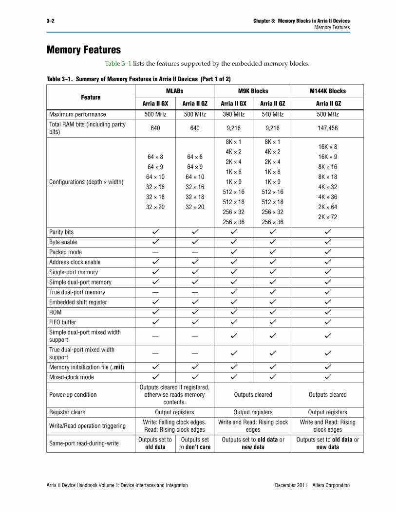
3–2 Chapter 3: Memory Blocks in Arria II DevicesMemory Features
r
Memory FeaturesTable 3–1 lists the features supported by the embedded memory blocks.
Table 3–1. Summary of Memory Features in Arria II Devices (Part 1 of 2)
FeatureMLABs M9K Blocks M144K Blocks
Arria II GX Arria II GZ Arria II GX Arria II GZ Arria II GZ
Maximum performance 500 MHz 500 MHz 390 MHz 540 MHz 500 MHz
Total RAM bits (including parity bits) 640 640 9,216 9,216 147,456
Configurations (depth × width)
64 × 8
64 × 9
64 × 10
32 × 16
32 × 18
32 × 20
64 × 8
64 × 9
64 × 10
32 × 16
32 × 18
32 × 20
8K × 1
4K × 2
2K × 4
1K × 8
1K × 9
512 × 16
512 × 18
256 × 32
256 × 36
8K × 1
4K × 2
2K × 4
1K × 8
1K × 9
512 × 16
512 × 18
256 × 32
256 × 36
16K × 8
16K × 9
8K × 16
8K × 18
4K × 32
4K × 36
2K × 64
2K × 72
Parity bits v v v v vByte enable v v v v vPacked mode — — v v vAddress clock enable v v v v vSingle-port memory v v v v vSimple dual-port memory v v v v vTrue dual-port memory — — v v vEmbedded shift register v v v v vROM v v v v vFIFO buffer v v v v vSimple dual-port mixed width support — — v v vTrue dual-port mixed width support — — v v vMemory initialization file (.mif) v v v v vMixed-clock mode v v v v v
Power-up conditionOutputs cleared if registered,
otherwise reads memory contents.
Outputs cleared Outputs cleared
Register clears Output registers Output registers Output registers
Write/Read operation triggering Write: Falling clock edges. Read: Rising clock edges
Write and Read: Rising clock edges
Write and Read: Rising clock edges
Same-port read-during-write Outputs set to old data
Outputs set to don’t care
Outputs set to old data or new data
Outputs set to old data onew data
Arria II Device Handbook Volume 1: Device Interfaces and Integration December 2011 Altera Corporation
Chapter 3: Memory Blocks in Arria II Devices 3–3Memory Features
rt
Table 3–2 lists the capacity and distribution of the memory blocks in each Arria II device.
Memory Block TypesM9K and M144K memory blocks are dedicated resources. MLABs are dual-purpose blocks. You can configure the MLABs as regular logic array blocks (LABs) or as MLABs. Ten ALMs make up one MLAB. You can configure each ALM in an MLAB as either a 64 × 1 or a 32 × 2 block, resulting in a 64 × 10 or 32 × 20 simple dual-port SRAM block in a single MLAB.
Parity Bit SupportAll memory blocks have built-in parity bit support. The ninth bit associated with each byte can store a parity bit or serve as an additional data bit. No parity function is actually performed on the ninth bit.
Byte Enable SupportAll memory blocks support byte enables that mask the input data so that only specific bytes of data are written. The unwritten bytes retain the previous written value. The write enable (wren) signals, along with the byte enable (byteena) signals, control the write operations of the RAM blocks.
Mixed-port read-during-writeOutputs set to old data,
new data, or don’t care
Outputs set to old data or don’t care
Outputs set to old data or don’t care
ECC Support Soft IP support using the Quartus II software
Soft IP support using the Quartus II software
Built-in support in ×64-wide simple dual-pomode or soft IP support
using the Quartus II software
Table 3–1. Summary of Memory Features in Arria II Devices (Part 2 of 2)
FeatureMLABs M9K Blocks M144K Blocks
Arria II GX Arria II GZ Arria II GX Arria II GZ Arria II GZ
Table 3–2. Memory Capacity and Distribution in Arria II Devices
Device MLABs M9K Blocks M144K Total RAM Bits (including MLABs) (Kbits)
EP2AGX45 903 319 — 3,435
EP2AGX65 1,265 495 — 5,246
EP2AGX95 1,874 612 — 6,679
EP2AGX125 2,482 730 — 8,121
EP2AGX190 3,806 840 — 9,939
EP2AGX260 5,130 950 — 11,756
EP2AGZ225 4,480 1,235 — 13,915
EP2AGZ300 5,960 1,248 24 18,413
EP2AGZ350 6,970 1,248 36 20,772
December 2011 Altera Corporation Arria II Device Handbook Volume 1: Device Interfaces and Integration
3–4 Chapter 3: Memory Blocks in Arria II DevicesMemory Features
The default value for the byte enable signals is high (enabled), in which case writing is controlled only by the write enable signals. The byte enable registers have no clear port. When using parity bits on the M9K and M144K blocks, the byte enable controls all 9 bits (8 bits of data plus 1 parity bit). When using parity bits on the MLAB, the byte-enable controls all 10 bits in the widest mode.
Byte enables are only supported for true dual-port memory configurations when both the PortA and PortB data widths of the individual M9K memory blocks are multiples of 8 or 9 bits. For example, you cannot use byte enable for a mixed data width memory configured with portA=32 and portB=8 because the mixed data width memory is implemented as 2 separate 16 x 4 bit memories.
Byte enables operate in a one-hot fashion, with the LSB of the byteena signal corresponding to the LSB of the data bus. For example, if you use a RAM block in ×18 mode, byteena = 01, data[8..0] is enabled and data[17..9] is disabled. Similarly, if byteena = 11, both data[8..0] and data[17..9] are enabled. Byte enables are active high.
1 You cannot use the byte enable feature when using the error correction coding (ECC) feature on M144K blocks.
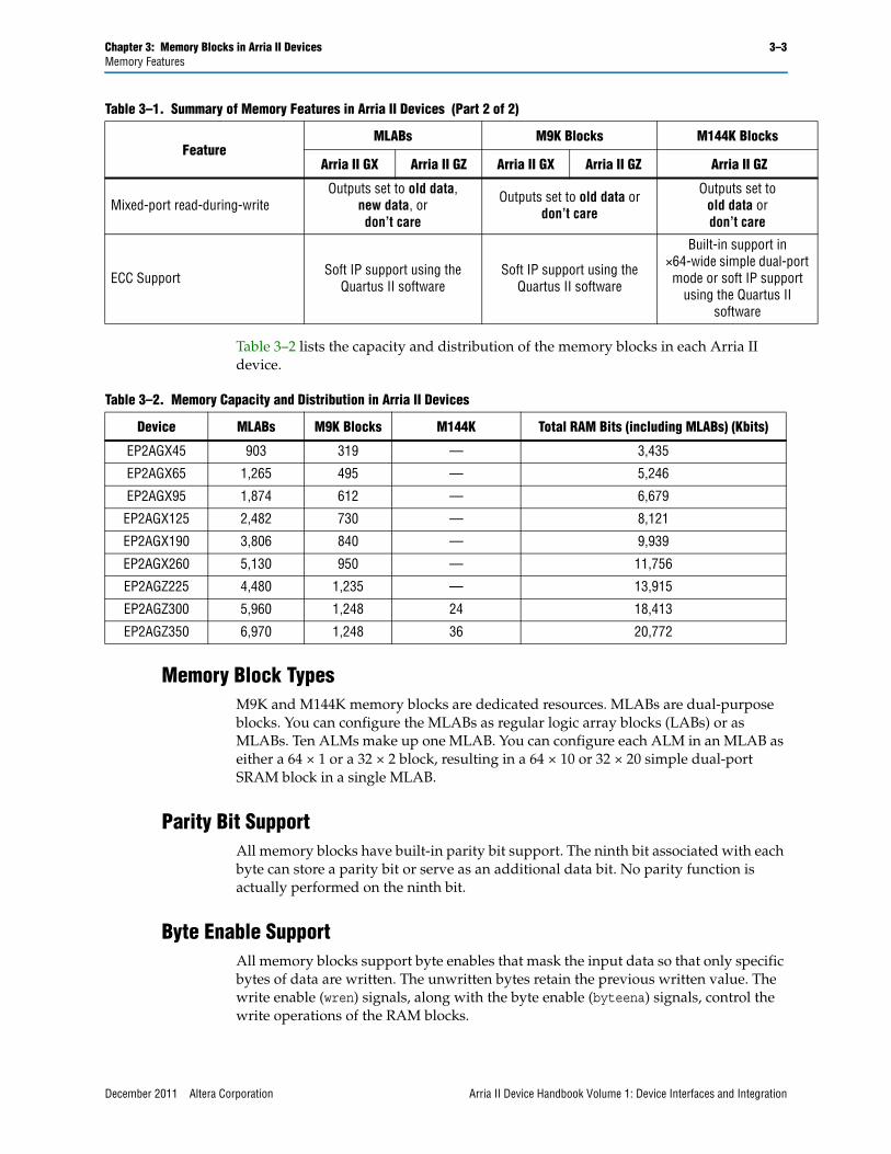
Figure 3–1 shows how the write enable (wren) and byte enable (byteena) signals control the operations of the M9K and M144K memory blocks.
When a byte-enable bit is deasserted during a write cycle, the corresponding data byte output can appear as either a “don’t care” value or the current data at that location. The output value for the masked byte is controllable using the Quartus II software. When a byte-enable bit is asserted during a write cycle, the corresponding data byte output also depends on the setting chosen in the Quartus II software.
Figure 3–1. Byte Enable Functional Waveform for M9K and M144K
inclock
wren
address
data
don't care: q (asynch)
byteena
XXXX ABCD XXXX
XX 10 01 11 XX
an a0 a1 a2 a0 a1 a2
ABCDFFFF
FFFF ABFF
FFFF FFCD
contents at a0
contents at a1
contents at a2
doutn ABXX XXCD ABCD ABFF FFCD ABCD
doutn ABFF FFCD ABCD ABFF FFCD ABCDcurrent data: q (asynch)
Arria II Device Handbook Volume 1: Device Interfaces and Integration December 2011 Altera Corporation
Chapter 3: Memory Blocks in Arria II Devices 3–5Memory Features
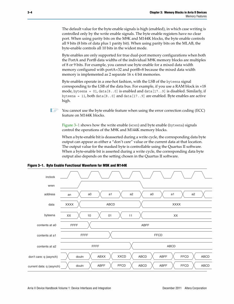
Figure 3–2 shows how the wren and byteena signals control the operations of the MLABs. Falling clock edges triggers the write operation in MLABs.
Packed Mode SupportArria II M9K and M144K blocks support packed mode. The packed mode feature packs two independent single-port RAMs into one memory block. The Quartus II software automatically implements the packed mode where appropriate by placing the physical RAM block into true dual-port mode and using the MSB of the address to distinguish between the two logical RAMs. The size of each independent single-port RAM must not exceed half of the target block size.
Address Clock Enable SupportArria II memory blocks support address clock enable, which holds the previous address value for as long as the signal is enabled (addressstall = 1). When you configure the memory blocks in dual-port mode, each port has its own independent address clock enable. The default value for the address clock enable signal is low (disabled).
Figure 3–2. Byte Enable Functional Waveform for MLABs
inclock
wren
address
data
byteena
XXXX ABCD XXXX
ABCDFFFF
FFFF ABFF
FFFF FFCD
contents at a0
contents at a1
contents at a2
current data: q (asynch) doutn FFFF FFCD ABCDFFFF ABFF FFCD FFCD
an a0 a1 a2 a0 a1 a2
XX 10 01 11 XX
ABFF FFFF
December 2011 Altera Corporation Arria II Device Handbook Volume 1: Device Interfaces and Integration
3–6 Chapter 3: Memory Blocks in Arria II DevicesMemory Features
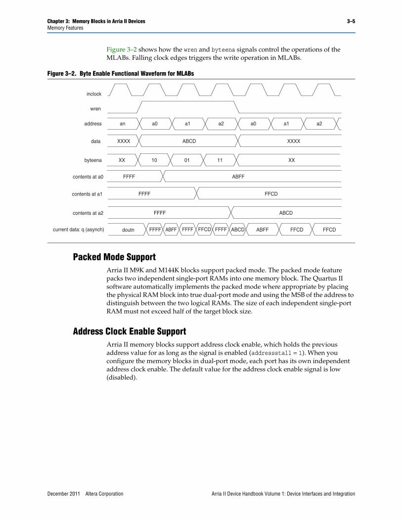
Figure 3–3 shows an address clock enable block diagram. The port name addressstall refers to the address clock enable.
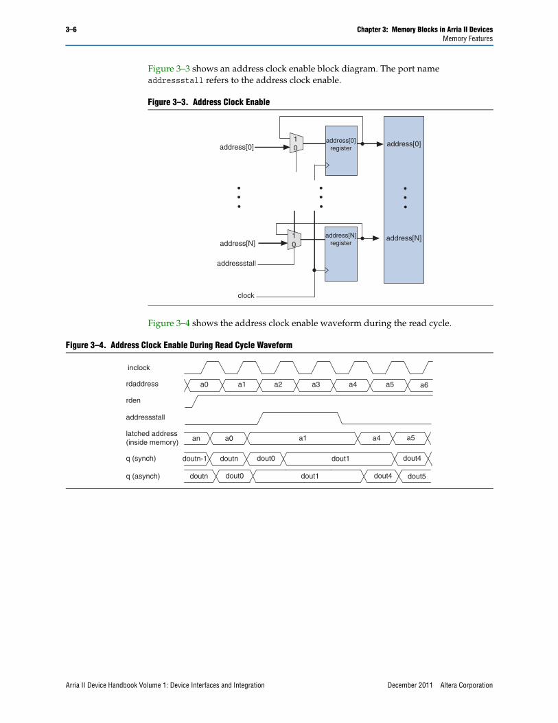
Figure 3–4 shows the address clock enable waveform during the read cycle.
Figure 3–3. Address Clock Enable
address[0]
address[N]
addressstall
clock
10
address[0]register
address[N]register
address[N]
address[0]
10
Figure 3–4. Address Clock Enable During Read Cycle Waveform
inclock
rden
rdaddress
q (synch)
a0 a1 a2 a3 a4 a5 a6
q (asynch)
an a0 a4 a5latched address(inside memory)
dout0 dout1 dout4
dout4 dout5
addressstall
a1
doutn-1 doutn
doutn dout0 dout1
Arria II Device Handbook Volume 1: Device Interfaces and Integration December 2011 Altera Corporation
Chapter 3: Memory Blocks in Arria II Devices 3–7Memory Features
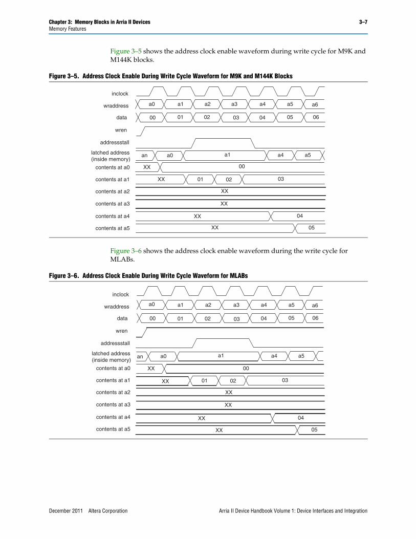
Figure 3–5 shows the address clock enable waveform during write cycle for M9K and M144K blocks.
Figure 3–6 shows the address clock enable waveform during the write cycle for MLABs.
Figure 3–5. Address Clock Enable During Write Cycle Waveform for M9K and M144K Blocks
inclock
wren
wraddress a0 a1 a2 a3 a4 a5 a6
an a0 a4 a5latched address(inside memory)
addressstall
a1
data 00 01 02 03 04 05 06
contents at a0
contents at a1
contents at a2
contents at a3
contents at a4
contents at a5
XX
04XX
00
0301XX 02
XX
XX
XX 05
Figure 3–6. Address Clock Enable During Write Cycle Waveform for MLABs
inclock
wren
wraddress a0 a1 a2 a3 a4 a5 a6
an a0 a4 a5latched address(inside memory)
addressstall
a1
data 00 01 02 03 04 05 06
contents at a0
contents at a1
contents at a2
contents at a3
contents at a4
contents at a5
XX
04XX
00
0301XX 02
XX
XX
XX 05
December 2011 Altera Corporation Arria II Device Handbook Volume 1: Device Interfaces and Integration
3–8 Chapter 3: Memory Blocks in Arria II DevicesMemory Features
Mixed Width SupportM9K and M144K blocks support mixed data widths inherently. MLABs can support mixed data widths through emulation with the Quartus II software. When using simple dual-port, true dual-port, or FIFO modes, mixed width support allows you to read and write different data widths to a memory block. For more information about the different widths supported per memory mode, refer to “Memory Modes” on page 3–10.
1 MLABs do not support mixed-width FIFO mode.
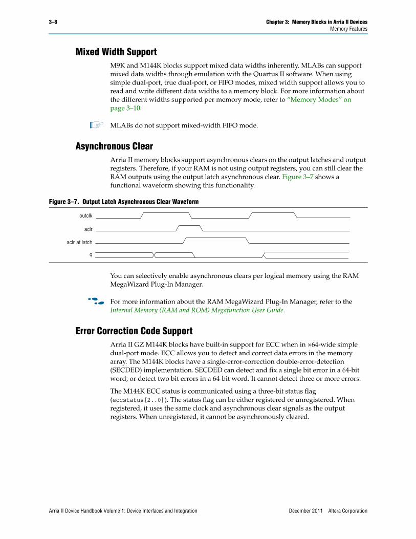
Asynchronous ClearArria II memory blocks support asynchronous clears on the output latches and output registers. Therefore, if your RAM is not using output registers, you can still clear the RAM outputs using the output latch asynchronous clear. Figure 3–7 shows a functional waveform showing this functionality.
You can selectively enable asynchronous clears per logical memory using the RAM MegaWizard Plug-In Manager.
f For more information about the RAM MegaWizard Plug-In Manager, refer to the Internal Memory (RAM and ROM) Megafunction User Guide.
Error Correction Code SupportArria II GZ M144K blocks have built-in support for ECC when in ×64-wide simple dual-port mode. ECC allows you to detect and correct data errors in the memory array. The M144K blocks have a single-error-correction double-error-detection (SECDED) implementation. SECDED can detect and fix a single bit error in a 64-bit word, or detect two bit errors in a 64-bit word. It cannot detect three or more errors.
The M144K ECC status is communicated using a three-bit status flag (eccstatus[2..0]). The status flag can be either registered or unregistered. When registered, it uses the same clock and asynchronous clear signals as the output registers. When unregistered, it cannot be asynchronously cleared.
Figure 3–7. Output Latch Asynchronous Clear Waveform
aclr
aclr at latch
q
outclk
Arria II Device Handbook Volume 1: Device Interfaces and Integration December 2011 Altera Corporation
Chapter 3: Memory Blocks in Arria II Devices 3–9Memory Features
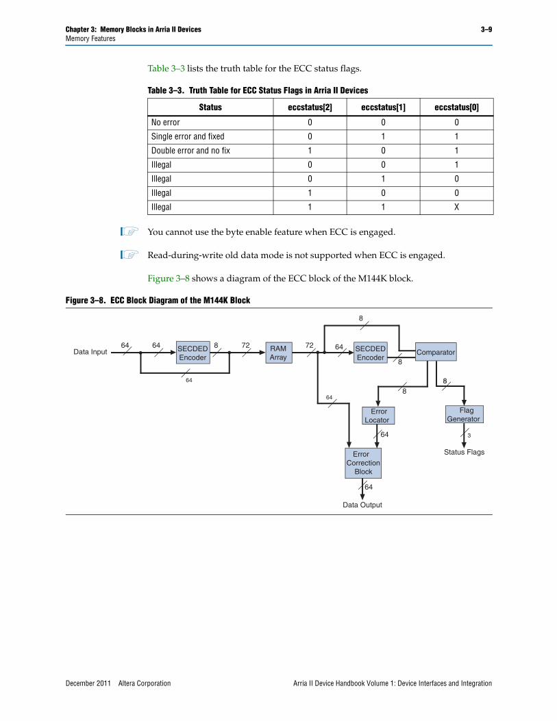
Table 3–3 lists the truth table for the ECC status flags.
1 You cannot use the byte enable feature when ECC is engaged.
1 Read-during-write old data mode is not supported when ECC is engaged.
Figure 3–8 shows a diagram of the ECC block of the M144K block.
Table 3–3. Truth Table for ECC Status Flags in Arria II Devices
Status eccstatus[2] eccstatus[1] eccstatus[0]
No error 0 0 0
Single error and fixed 0 1 1
Double error and no fix 1 0 1
Illegal 0 0 1
Illegal 0 1 0
Illegal 1 0 0
Illegal 1 1 X
Figure 3–8. ECC Block Diagram of the M144K Block
Data Input64 64
64
8 72SECDEDEncoder
RAMArray
72 64
64
8
8
888
64
64 3
Status Flags
Data Output
SECDEDEncoder
Comparator
ErrorCorrection Block
ErrorLocator
FlagGenerator
December 2011 Altera Corporation Arria II Device Handbook Volume 1: Device Interfaces and Integration
3–10 Chapter 3: Memory Blocks in Arria II DevicesMemory Modes
Memory ModesArria II memory blocks allow you to implement fully synchronous SRAM memory in multiple modes of operation. M9K and M144K blocks do not support asynchronous memory (unregistered inputs). MLABs support asynchronous (flow-through) read operations.
Depending on which memory block you target, you can use the following modes:
■ “Single-Port RAM Mode” on page 3–10
■ “Simple Dual-Port Mode” on page 3–12
■ “True Dual-Port Mode” on page 3–15
■ “Shift-Register Mode” on page 3–17
■ “ROM Mode” on page 3–18
■ “FIFO Mode” on page 3–18
1 To choose the desired read-during-write behavior, set the read-during-write behavior to either new data, old data, or don't care in the RAM MegaWizard Plug-In Manager in the Quartus II software. For more information about this behavior, refer to “Read-During-Write Behavior” on page 3–21.
1 When using the memory blocks in ROM, single-port, simple dual-port, or true dual-port mode, you can corrupt the memory contents if you violate the setup or hold time on any of the memory block input registers. This applies to both read and write operations.
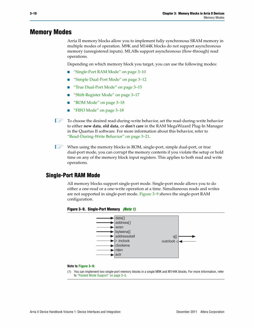
Single-Port RAM ModeAll memory blocks support single-port mode. Single-port mode allows you to do either a one-read or a one-write operation at a time. Simultaneous reads and writes are not supported in single-port mode. Figure 3–9 shows the single-port RAM configuration.
Figure 3–9. Single-Port Memory (Note 1)
Note to Figure 3–9:
(1) You can implement two single-port memory blocks in a single M9K and M144K blocks. For more information, refer to “Packed Mode Support” on page 3–5.
data[ ]address[ ]wrenbyteena[]addressstall inclockclockenardenaclr
outclockq[]
Arria II Device Handbook Volume 1: Device Interfaces and Integration December 2011 Altera Corporation
Chapter 3: Memory Blocks in Arria II Devices 3–11Memory Modes
During a write operation, the RAM output behavior is configurable. If you use the read-enable signal and perform a write operation with the read enable deactivated, the RAM outputs retain the values they held during the most recent active read enable. If you activate read enable during a write operation, or if you do not use the read-enable signal at all, the RAM outputs show the “new data” being written, the “old data” at that address, or a “don’t care” value.
Table 3–4 lists the possible port width configurations for memory blocks in single-port mode.
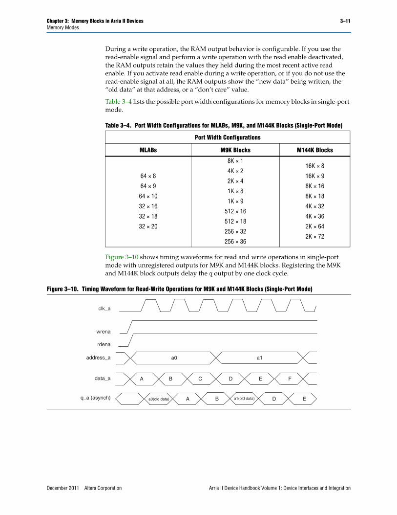
Figure 3–10 shows timing waveforms for read and write operations in single-port mode with unregistered outputs for M9K and M144K blocks. Registering the M9K and M144K block outputs delay the q output by one clock cycle.
Table 3–4. Port Width Configurations for MLABs, M9K, and M144K Blocks (Single-Port Mode)
Port Width Configurations
MLABs M9K Blocks M144K Blocks
64 × 8
64 × 9
64 × 10
32 × 16
32 × 18
32 × 20
8K × 1
4K × 2
2K × 4
1K × 8
1K × 9
512 × 16
512 × 18
256 × 32
256 × 36
16K × 8
16K × 9
8K × 16
8K × 18
4K × 32
4K × 36
2K × 64
2K × 72
Figure 3–10. Timing Waveform for Read-Write Operations for M9K and M144K Blocks (Single-Port Mode)
clk_a
wrena
address_a
data_a
rdena
q_a (asynch)
a0 a1
A B C D E F
a0(old data) a1(old data)A B D E
December 2011 Altera Corporation Arria II Device Handbook Volume 1: Device Interfaces and Integration
3–12 Chapter 3: Memory Blocks in Arria II DevicesMemory Modes
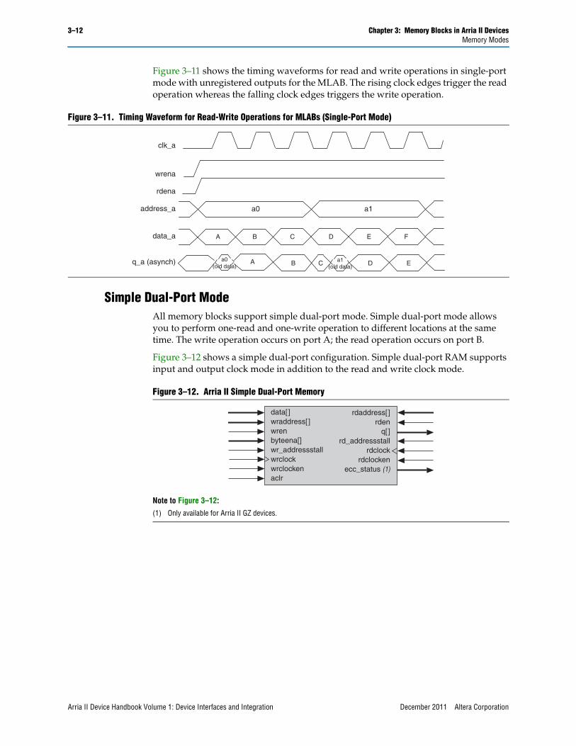
Figure 3–11 shows the timing waveforms for read and write operations in single-port mode with unregistered outputs for the MLAB. The rising clock edges trigger the read operation whereas the falling clock edges triggers the write operation.
Simple Dual-Port ModeAll memory blocks support simple dual-port mode. Simple dual-port mode allows you to perform one-read and one-write operation to different locations at the same time. The write operation occurs on port A; the read operation occurs on port B.
Figure 3–12 shows a simple dual-port configuration. Simple dual-port RAM supports input and output clock mode in addition to the read and write clock mode.
Figure 3–11. Timing Waveform for Read-Write Operations for MLABs (Single-Port Mode)
clk_a
wrena
address_a
data_a
rdena
q_a (asynch)
a0 a1
A B C D E F
a0(old data)
A B D Ea1(old data)C
Figure 3–12. Arria II Simple Dual-Port Memory
Note to Figure 3–12:
(1) Only available for Arria II GZ devices.
data[ ]wraddress[ ]wrenbyteena[]wr_addressstallwrclockwrclockenaclr
rdaddress[ ]rden
q[ ]rd_addressstall
rdclockrdclocken
ecc_status (1)
Arria II Device Handbook Volume 1: Device Interfaces and Integration December 2011 Altera Corporation
Chapter 3: Memory Blocks in Arria II Devices 3–13Memory Modes
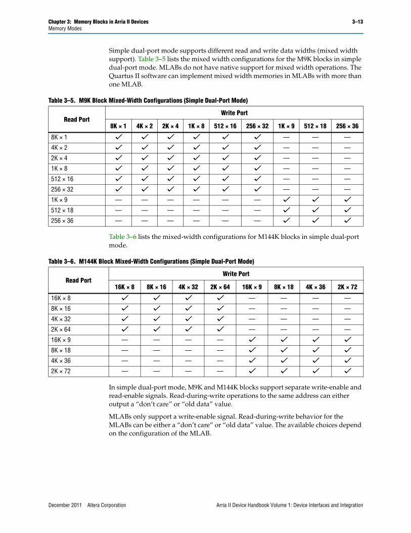
Simple dual-port mode supports different read and write data widths (mixed width support). Table 3–5 lists the mixed width configurations for the M9K blocks in simple dual-port mode. MLABs do not have native support for mixed width operations. The Quartus II software can implement mixed width memories in MLABs with more than one MLAB.
Table 3–6 lists the mixed-width configurations for M144K blocks in simple dual-port mode.
In simple dual-port mode, M9K and M144K blocks support separate write-enable and read-enable signals. Read-during-write operations to the same address can either output a “don’t care” or “old data” value.
MLABs only support a write-enable signal. Read-during-write behavior for the MLABs can be either a “don’t care” or “old data” value. The available choices depend on the configuration of the MLAB.
Table 3–5. M9K Block Mixed-Width Configurations (Simple Dual-Port Mode)
Read PortWrite Port
8K × 1 4K × 2 2K × 4 1K × 8 512 × 16 256 × 32 1K × 9 512 × 18 256 × 36
8K × 1 v v v v v v — — —
4K × 2 v v v v v v — — —
2K × 4 v v v v v v — — —
1K × 8 v v v v v v — — —
512 × 16 v v v v v v — — —
256 × 32 v v v v v v — — —
1K × 9 — — — — — — v v v512 × 18 — — — — — — v v v256 × 36 — — — — — — v v v
Table 3–6. M144K Block Mixed-Width Configurations (Simple Dual-Port Mode)
Read PortWrite Port
16K × 8 8K × 16 4K × 32 2K × 64 16K × 9 8K × 18 4K × 36 2K × 72
16K × 8 v v v v — — — —
8K × 16 v v v v — — — —
4K × 32 v v v v — — — —
2K × 64 v v v v — — — —
16K × 9 — — — — v v v v8K × 18 — — — — v v v v4K × 36 — — — — v v v v2K × 72 — — — — v v v v
December 2011 Altera Corporation Arria II Device Handbook Volume 1: Device Interfaces and Integration
3–14 Chapter 3: Memory Blocks in Arria II DevicesMemory Modes
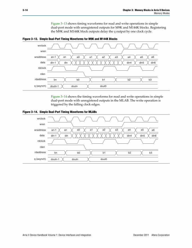
Figure 3–13 shows timing waveforms for read and write operations in simple dual-port mode with unregistered outputs for M9K and M144K blocks. Registering the M9K and M144K block outputs delay the q output by one clock cycle.
Figure 3–14 shows the timing waveforms for read and write operations in simple dual-port mode with unregistered outputs in the MLAB. The write operation is triggered by the falling clock edges.
Figure 3–13. Simple Dual-Port Timing Waveforms for M9K and M144K Blocks
wrclock
wren
wraddress
rdclock
an-1 an a0 a1 a2 a3 a4 a5 a6
q (asynch)
rden
rdaddress bn b0 b1 b2 b3
doutn-1 doutn dout0
din-1 din din4 din5 din6data
Figure 3–14. Simple Dual-Port Timing Waveforms for MLABs
wrclock
wren
wraddress
rdclock
an-1 an a0 a1 a2 a3 a4 a5 a6
q (asynch)
rden
rdaddress bn b0 b1 b2 b3
doutn-1 doutn dout0
din-1 din din4 din5 din6data
Arria II Device Handbook Volume 1: Device Interfaces and Integration December 2011 Altera Corporation
Chapter 3: Memory Blocks in Arria II Devices 3–15Memory Modes
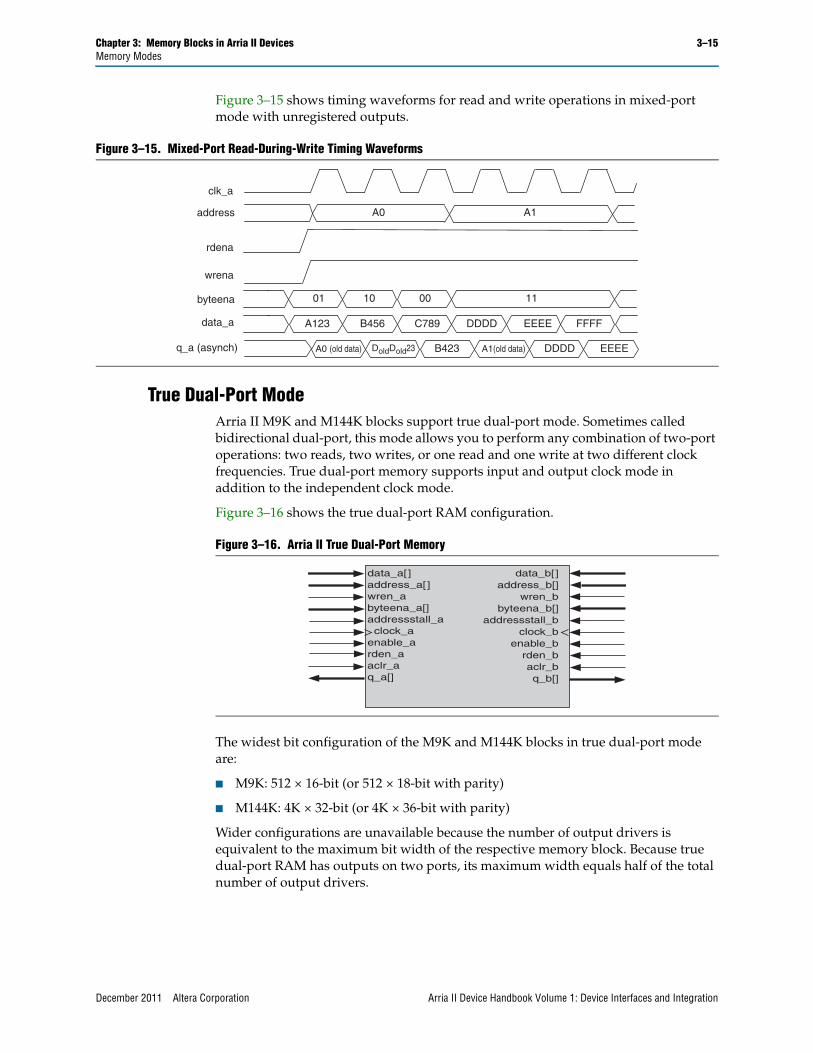
Figure 3–15 shows timing waveforms for read and write operations in mixed-port mode with unregistered outputs.
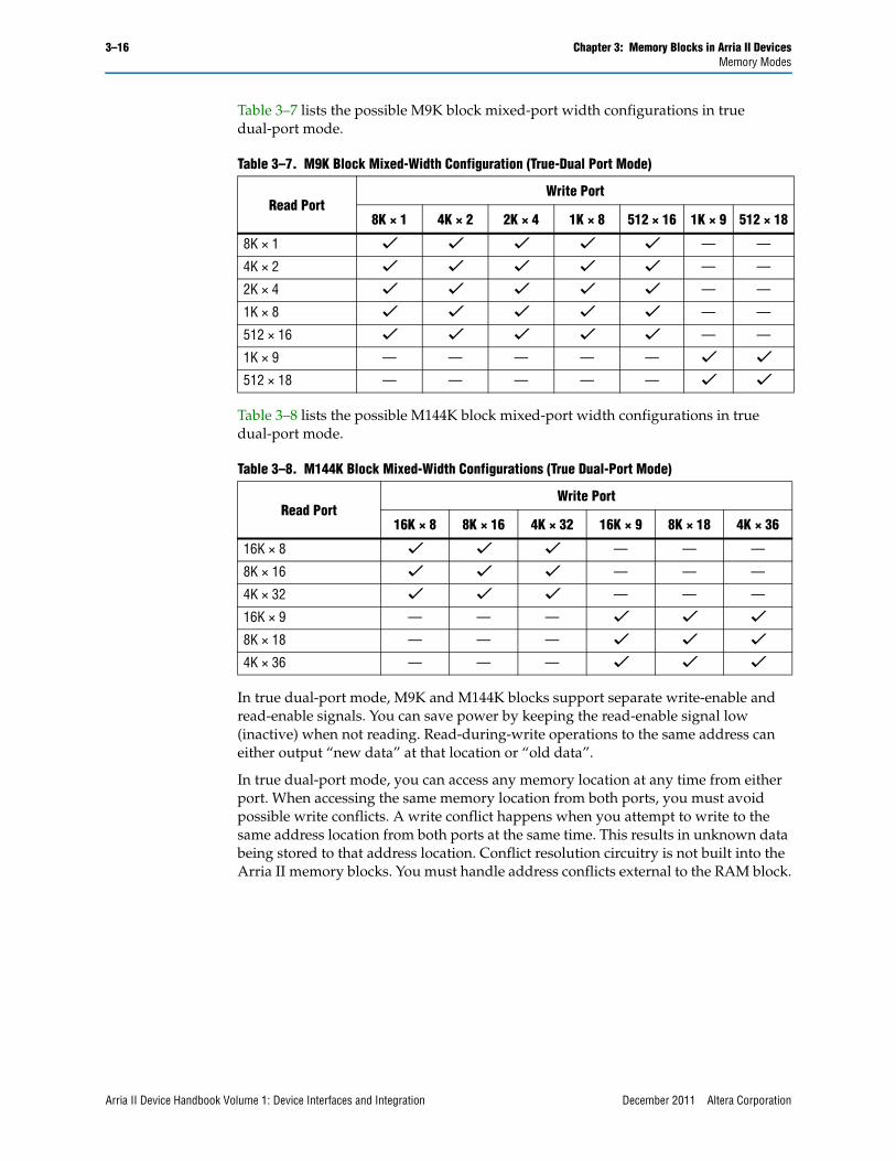
True Dual-Port ModeArria II M9K and M144K blocks support true dual-port mode. Sometimes called bidirectional dual-port, this mode allows you to perform any combination of two-port operations: two reads, two writes, or one read and one write at two different clock frequencies. True dual-port memory supports input and output clock mode in addition to the independent clock mode.
Figure 3–16 shows the true dual-port RAM configuration.
The widest bit configuration of the M9K and M144K blocks in true dual-port mode are:
■ M9K: 512 × 16-bit (or 512 × 18-bit with parity)
■ M144K: 4K × 32-bit (or 4K × 36-bit with parity)
Wider configurations are unavailable because the number of output drivers is equivalent to the maximum bit width of the respective memory block. Because true dual-port RAM has outputs on two ports, its maximum width equals half of the total number of output drivers.
Figure 3–15. Mixed-Port Read-During-Write Timing Waveforms
clk_a
wrena
rdena
address A0 A1
byteena 01 10 00 11
data_a A123 B456 C789 DDDD EEEE FFFF
q_a (asynch) A0 (old data) A1(old data) DDDD EEEEB423DoldDold23
Figure 3–16. Arria II True Dual-Port Memory
data_a[ ]address_a[ ]wren_abyteena_a[]addressstall_a clock_aenable_a rden_aaclr_aq_a[]
data_b[ ]address_b[]
wren_bbyteena_b[]
addressstall_bclock_b
enable_brden_baclr_bq_b[]
December 2011 Altera Corporation Arria II Device Handbook Volume 1: Device Interfaces and Integration
3–16 Chapter 3: Memory Blocks in Arria II DevicesMemory Modes
Table 3–7 lists the possible M9K block mixed-port width configurations in true dual-port mode.
Table 3–8 lists the possible M144K block mixed-port width configurations in true dual-port mode.
In true dual-port mode, M9K and M144K blocks support separate write-enable and read-enable signals. You can save power by keeping the read-enable signal low (inactive) when not reading. Read-during-write operations to the same address can either output “new data” at that location or “old data”.
In true dual-port mode, you can access any memory location at any time from either port. When accessing the same memory location from both ports, you must avoid possible write conflicts. A write conflict happens when you attempt to write to the same address location from both ports at the same time. This results in unknown data being stored to that address location. Conflict resolution circuitry is not built into the Arria II memory blocks. You must handle address conflicts external to the RAM block.
Table 3–7. M9K Block Mixed-Width Configuration (True-Dual Port Mode)
Read PortWrite Port
8K × 1 4K × 2 2K × 4 1K × 8 512 × 16 1K × 9 512 × 18
8K × 1 v v v v v — —
4K × 2 v v v v v — —
2K × 4 v v v v v — —
1K × 8 v v v v v — —
512 × 16 v v v v v — —
1K × 9 — — — — — v v512 × 18 — — — — — v v
Table 3–8. M144K Block Mixed-Width Configurations (True Dual-Port Mode)
Read PortWrite Port
16K × 8 8K × 16 4K × 32 16K × 9 8K × 18 4K × 36
16K × 8 v v v — — —
8K × 16 v v v — — —
4K × 32 v v v — — —
16K × 9 — — — v v v8K × 18 — — — v v v4K × 36 — — — v v v
Arria II Device Handbook Volume 1: Device Interfaces and Integration December 2011 Altera Corporation
Chapter 3: Memory Blocks in Arria II Devices 3–17Memory Modes
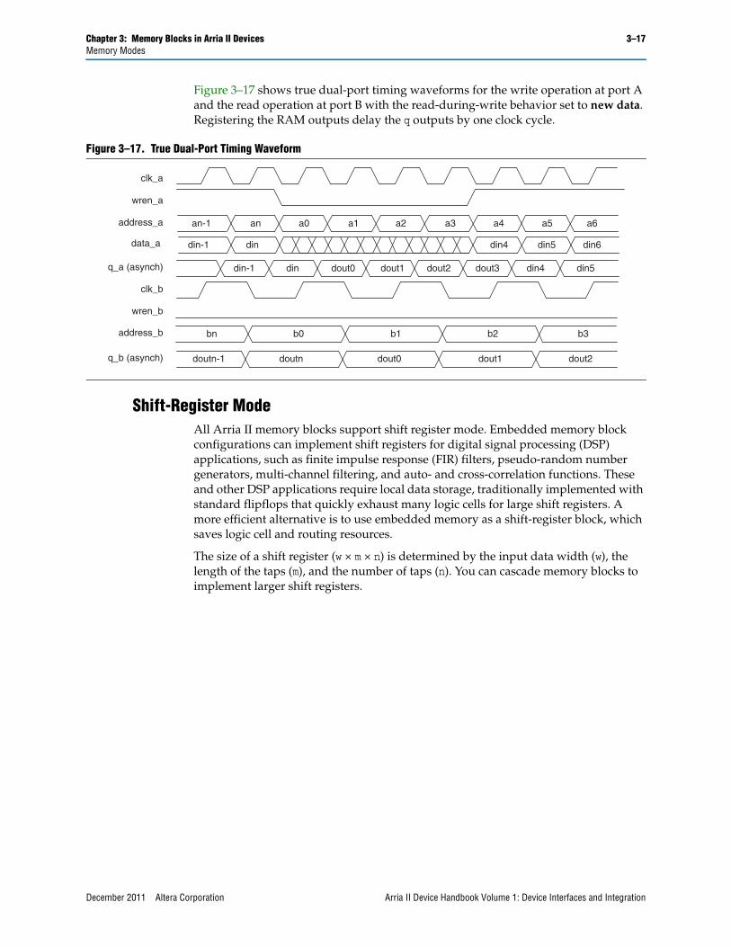
Figure 3–17 shows true dual-port timing waveforms for the write operation at port A and the read operation at port B with the read-during-write behavior set to new data. Registering the RAM outputs delay the q outputs by one clock cycle.
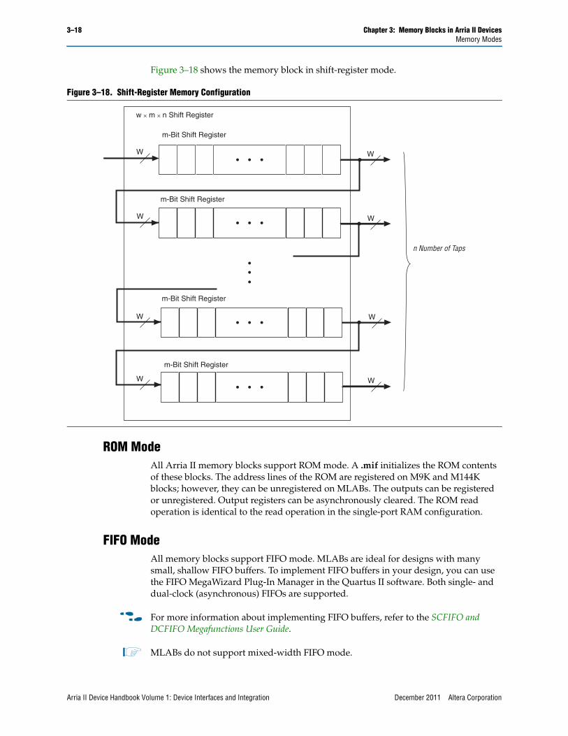
Shift-Register ModeAll Arria II memory blocks support shift register mode. Embedded memory block configurations can implement shift registers for digital signal processing (DSP) applications, such as finite impulse response (FIR) filters, pseudo-random number generators, multi-channel filtering, and auto- and cross-correlation functions. These and other DSP applications require local data storage, traditionally implemented with standard flipflops that quickly exhaust many logic cells for large shift registers. A more efficient alternative is to use embedded memory as a shift-register block, which saves logic cell and routing resources.
The size of a shift register (w × m × n) is determined by the input data width (w), the length of the taps (m), and the number of taps (n). You can cascade memory blocks to implement larger shift registers.
Figure 3–17. True Dual-Port Timing Waveform
clk_a
wren_a
address_a
clk_b
an-1 an a0 a1 a2 a3 a4 a5 a6
q_b (asynch)
wren_b
address_b bn b0 b1 b2 b3
doutn-1 doutn dout0
q_a (asynch)
din-1 din din4 din5 din6data_a
din-1 din dout0 dout1 dout2 dout3 din4 din5
dout2dout1
December 2011 Altera Corporation Arria II Device Handbook Volume 1: Device Interfaces and Integration
3–18 Chapter 3: Memory Blocks in Arria II DevicesMemory Modes
Figure 3–18 shows the memory block in shift-register mode.
ROM ModeAll Arria II memory blocks support ROM mode. A .mif initializes the ROM contents of these blocks. The address lines of the ROM are registered on M9K and M144K blocks; however, they can be unregistered on MLABs. The outputs can be registered or unregistered. Output registers can be asynchronously cleared. The ROM read operation is identical to the read operation in the single-port RAM configuration.
FIFO ModeAll memory blocks support FIFO mode. MLABs are ideal for designs with many small, shallow FIFO buffers. To implement FIFO buffers in your design, you can use the FIFO MegaWizard Plug-In Manager in the Quartus II software. Both single- and dual-clock (asynchronous) FIFOs are supported.
f For more information about implementing FIFO buffers, refer to the SCFIFO and DCFIFO Megafunctions User Guide.
1 MLABs do not support mixed-width FIFO mode.
Figure 3–18. Shift-Register Memory Configuration
W
w × m × n Shift Register
m-Bit Shift Register
m-Bit Shift Register
m-Bit Shift Register
m-Bit Shift Register
W
W
W
W
W
W
W
n Number of Taps
Arria II Device Handbook Volume 1: Device Interfaces and Integration December 2011 Altera Corporation
Chapter 3: Memory Blocks in Arria II Devices 3–19Clocking Modes
Clocking ModesArria II memory blocks support the following clocking modes:
■ “Independent Clock Mode” on page 3–19
■ “Input and Output Clock Mode” on page 3–19
■ “Read and Write Clock Mode” on page 3–19
■ “Single Clock Mode” on page 3–20
c Violating the setup or hold time on the memory block address registers could corrupt the memory contents. This applies to both read and write operations.
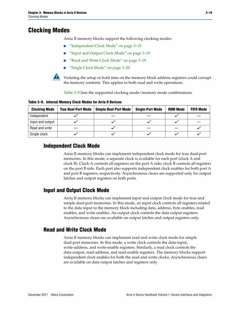
Table 3–9 lists the supported clocking mode/memory mode combinations.
Independent Clock ModeArria II memory blocks can implement independent clock mode for true dual-port memories. In this mode, a separate clock is available for each port (clock A and clock B). Clock A controls all registers on the port A side; clock B controls all registers on the port B side. Each port also supports independent clock enables for both port A and port B registers, respectively. Asynchronous clears are supported only for output latches and output registers on both ports.
Input and Output Clock ModeArria II memory blocks can implement input and output clock mode for true and simple dual-port memories. In this mode, an input clock controls all registers related to the data input to the memory block including data, address, byte enables, read enables, and write enables. An output clock controls the data output registers. Asynchronous clears are available on output latches and output registers only.
Read and Write Clock ModeArria II memory blocks can implement read and write clock mode for simple dual-port memories. In this mode, a write clock controls the data-input, write-address, and write-enable registers. Similarly, a read clock controls the data-output, read-address, and read-enable registers. The memory blocks support independent clock enables for both the read and write clocks. Asynchronous clears are available on data output latches and registers only.
Table 3–9. Internal Memory Clock Modes for Arria II Devices
Clocking Mode True Dual-Port Mode Simple Dual-Port Mode Single-Port Mode ROM Mode FIFO Mode
Independent v — — v —
Input and output v v v v —
Read and write — v — — vSingle clock v v v v v
December 2011 Altera Corporation Arria II Device Handbook Volume 1: Device Interfaces and Integration
3–20 Chapter 3: Memory Blocks in Arria II DevicesDesign Considerations
When using read and write clock mode, the output read data is unknown if you perform a simultaneous read and write to the same address location. If you require the output data to be a known value, use either single clock mode or input and output clock mode, and choose the appropriate read-during-write behavior in the MegaWizard Plug-In Manager.
Single Clock ModeArria II memory blocks can implement single clock mode for true dual-port, simple dual-port, and single-port memories. In this mode, a single clock, together with a clock enable, is used to control all registers of the memory block. Asynchronous clears are available on output latches and output registers only.
Design ConsiderationsThis section describes guidelines for designing with memory blocks.
Selecting Memory BlockThe Quartus II software automatically partitions user-defined memory into embedded memory blocks by taking into account both speed and size constraints placed on your design. For example, the Quartus II software may spread out memory across multiple memory blocks when resources are available to increase the performance of your design. You can manually assign memory to a specific block size using the RAM MegaWizard Plug-In Manager.
MLABs can implement single-port SRAM through emulation with the Quartus II software. Emulation results in minimal additional logic resources used. Because of the dual-purpose architecture of the MLAB, it only has data input registers and output registers in the block. MLABs gain input address registers and additional optional data output registers from adjacent ALMs with register packing.
f For more information about register packing, refer to the Logic Array Blocks and Adaptive Logic Modules in Arria II Devices chapter.
Conflict ResolutionWhen using the memory blocks in true dual-port mode, it is possible to attempt two write operations to the same memory location (address). Because there is no conflict resolution circuitry built into the memory blocks, this results in unknown data being written to that location. Therefore, you must implement conflict resolution logic, external to the memory block, to avoid address conflicts.
Arria II Device Handbook Volume 1: Device Interfaces and Integration December 2011 Altera Corporation
Chapter 3: Memory Blocks in Arria II Devices 3–21Design Considerations
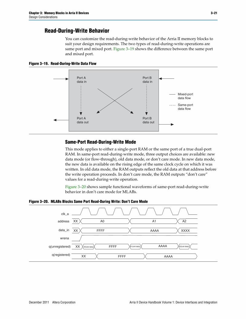
Read-During-Write BehaviorYou can customize the read-during-write behavior of the Arria II memory blocks to suit your design requirements. The two types of read-during-write operations are same port and mixed port. Figure 3–19 shows the difference between the same port and mixed port.
Same-Port Read-During-Write ModeThis mode applies to either a single-port RAM or the same port of a true dual-port RAM. In same-port read-during-write mode, three output choices are available: new data mode (or flow-through), old data mode, or don’t care mode. In new data mode, the new data is available on the rising edge of the same clock cycle on which it was written. In old data mode, the RAM outputs reflect the old data at that address before the write operation proceeds. In don’t care mode, the RAM outputs “don’t care” values for a read-during-write operation.
Figure 3–20 shows sample functional waveforms of same-port read-during-write behavior in don’t care mode for MLABs.
Figure 3–19. Read-During-Write Data Flow
Port Adata in
Port Bdata in
Port Adata out
Port Bdata out
Mixed-portdata flow
Same-portdata flow
Figure 3–20. MLABs Blocks Same Port Read-During Write: Don’t Care Mode
clk_a
wrena
data_in
address A1
q(unregistered) A0(old data)
A2
FFFF AAAA XXXX
XX FFFF AAAAA1(old data) A2(old data)
q(registered) FFFF AAAA
A0
XX
XX
XX
December 2011 Altera Corporation Arria II Device Handbook Volume 1: Device Interfaces and Integration
3–22 Chapter 3: Memory Blocks in Arria II DevicesDesign Considerations
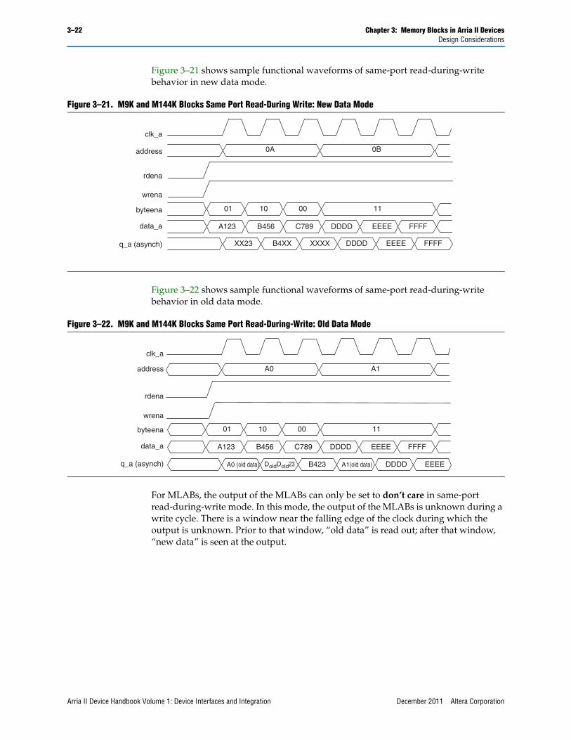
Figure 3–21 shows sample functional waveforms of same-port read-during-write behavior in new data mode.
Figure 3–22 shows sample functional waveforms of same-port read-during-write behavior in old data mode.
For MLABs, the output of the MLABs can only be set to don’t care in same-port read-during-write mode. In this mode, the output of the MLABs is unknown during a write cycle. There is a window near the falling edge of the clock during which the output is unknown. Prior to that window, “old data” is read out; after that window, “new data” is seen at the output.
Figure 3–21. M9K and M144K Blocks Same Port Read-During Write: New Data Mode
clk_a
wrena
rdena
address 0A 0B
byteena 01 10 00 11
data_a A123 B456 C789 DDDD EEEE FFFF
q_a (asynch) XX23 B4XX XXXX DDDD EEEE FFFF
Figure 3–22. M9K and M144K Blocks Same Port Read-During-Write: Old Data Mode
clk_a
wrena
rdena
address A0 A1
byteena 01 10 00 11
data_a A123 B456 C789 DDDD EEEE FFFF
q_a (asynch) A0 (old data) A1(old data) DDDD EEEEB423DoldDold23
Arria II Device Handbook Volume 1: Device Interfaces and Integration December 2011 Altera Corporation
Chapter 3: Memory Blocks in Arria II Devices 3–23Design Considerations
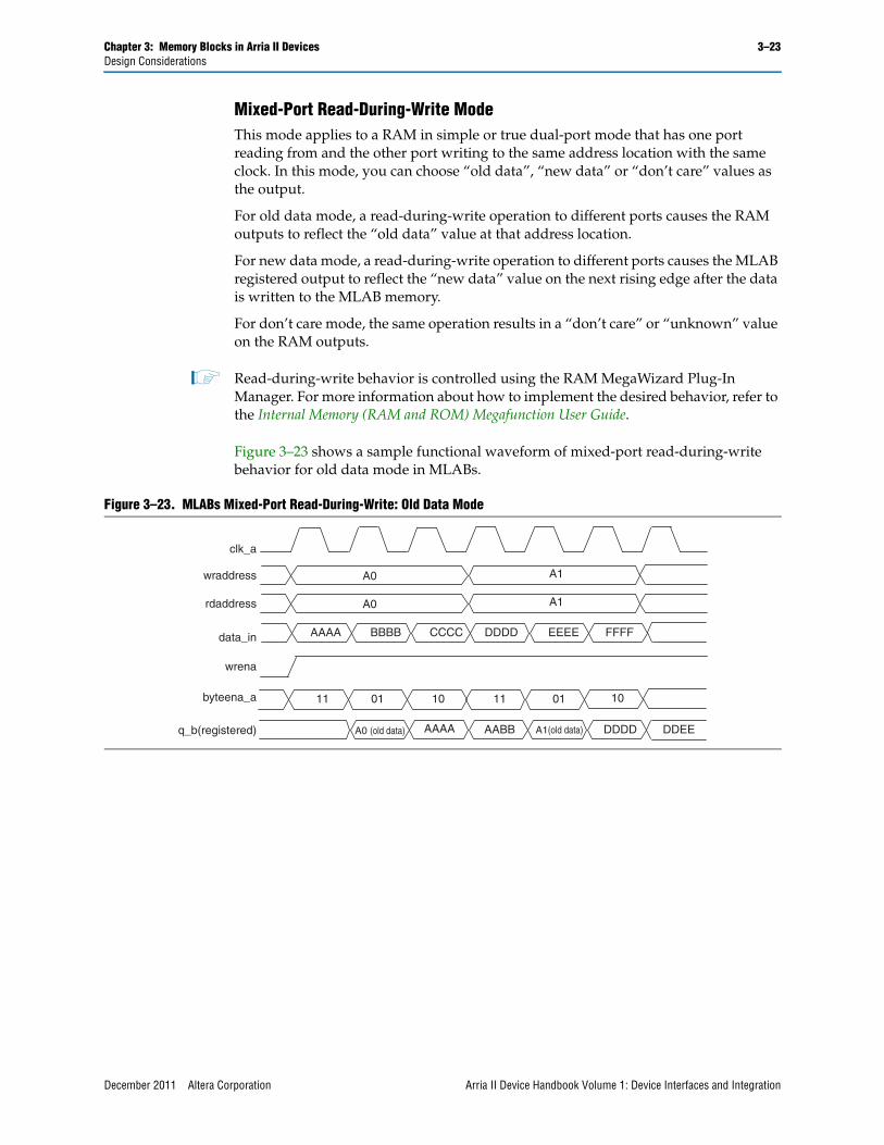
Mixed-Port Read-During-Write ModeThis mode applies to a RAM in simple or true dual-port mode that has one port reading from and the other port writing to the same address location with the same clock. In this mode, you can choose “old data”, “new data” or “don’t care” values as the output.
For old data mode, a read-during-write operation to different ports causes the RAM outputs to reflect the “old data” value at that address location.
For new data mode, a read-during-write operation to different ports causes the MLAB registered output to reflect the “new data” value on the next rising edge after the data is written to the MLAB memory.
For don’t care mode, the same operation results in a “don’t care” or “unknown” value on the RAM outputs.
1 Read-during-write behavior is controlled using the RAM MegaWizard Plug-In Manager. For more information about how to implement the desired behavior, refer to the Internal Memory (RAM and ROM) Megafunction User Guide.
Figure 3–23 shows a sample functional waveform of mixed-port read-during-write behavior for old data mode in MLABs.
Figure 3–23. MLABs Mixed-Port Read-During-Write: Old Data Mode
clk_a
wrena
data_in
wraddress A1
byteena_a
q_b(registered)
A0
rdaddress A1A0
AAAA BBBB CCCC DDDD EEEE FFFF
A0 (old data) A1(old data) DDDDAABBAAAA
11 01 10 11 01 10
DDEE
December 2011 Altera Corporation Arria II Device Handbook Volume 1: Device Interfaces and Integration
3–24 Chapter 3: Memory Blocks in Arria II DevicesDesign Considerations
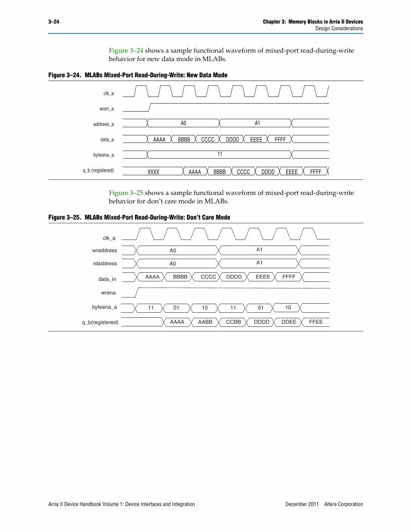
Figure 3–24 shows a sample functional waveform of mixed-port read-during-write behavior for new data mode in MLABs.
Figure 3–25 shows a sample functional waveform of mixed-port read-during-write behavior for don’t care mode in MLABs.
Figure 3–24. MLABs Mixed-Port Read-During-Write: New Data Mode
XXXX
11
clk_a
address_a
wren_a
byteena_a
data_a
q_b (registered)
AAAA BBBB CCCC DDDD EEEE FFFF
1A0A
AAAA BBBB CCCC DDDD EEEE FFFF
Figure 3–25. MLABs Mixed-Port Read-During-Write: Don’t Care Mode
clk_a
wrena
data_in
wraddress A1
byteena_a
q_b(registered)
A0
rdaddress A1A0
AAAA BBBB CCCC DDDD EEEE FFFF
AAAA DDDD DDEECCBBAABB
11 01 10 11 01 10
FFEE
Arria II Device Handbook Volume 1: Device Interfaces and Integration December 2011 Altera Corporation
Chapter 3: Memory Blocks in Arria II Devices 3–25Design Considerations
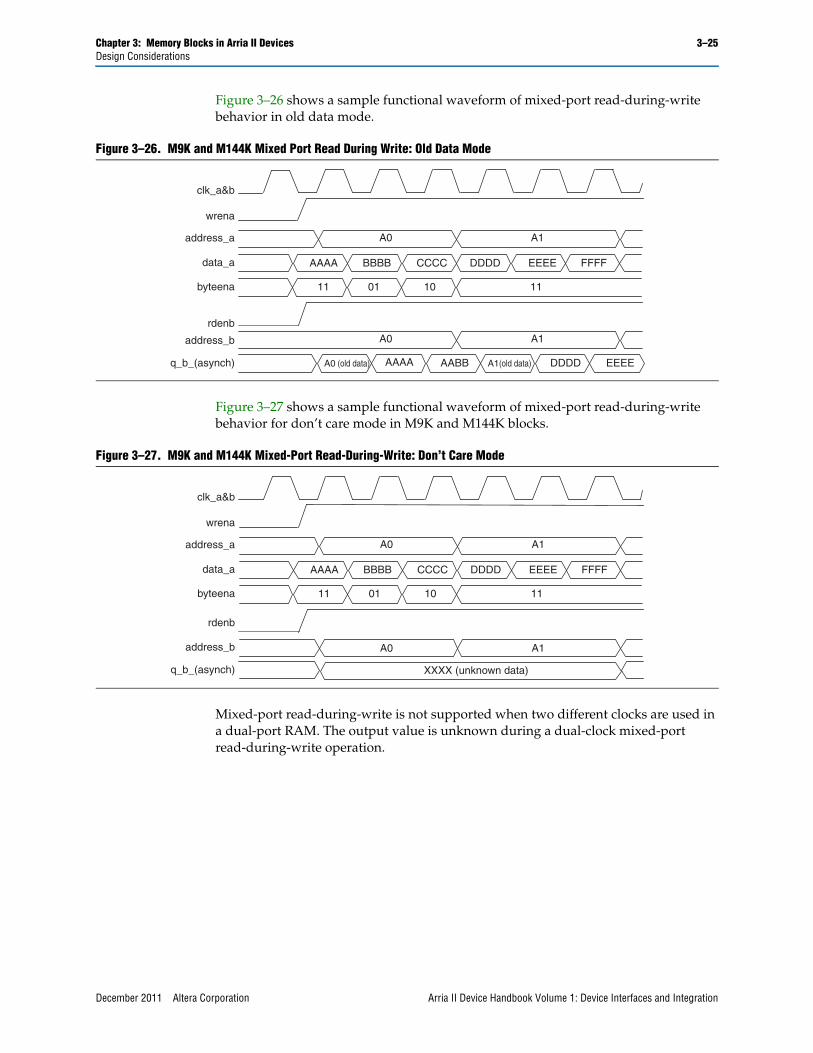
Figure 3–26 shows a sample functional waveform of mixed-port read-during-write behavior in old data mode.
Figure 3–27 shows a sample functional waveform of mixed-port read-during-write behavior for don’t care mode in M9K and M144K blocks.
Mixed-port read-during-write is not supported when two different clocks are used in a dual-port RAM. The output value is unknown during a dual-clock mixed-port read-during-write operation.
Figure 3–26. M9K and M144K Mixed Port Read During Write: Old Data Mode
clk_a&b
wrena
rdenb
address_a A0 A1
byteena 11 01 10 11
data_a AAAA BBBB CCCC DDDD EEEE FFFF
q_b_(asynch) A0 (old data) A1(old data) DDDD EEEEAABBAAAA
address_b A0 A1
Figure 3–27. M9K and M144K Mixed-Port Read-During-Write: Don’t Care Mode
clk_a&b
wrena
rdenb
address_a A0 A1
byteena 11 01 10 11
data_a AAAA BBBB CCCC DDDD EEEE FFFF
q_b_(asynch) XXXX (unknown data)
address_b A0 A1
December 2011 Altera Corporation Arria II Device Handbook Volume 1: Device Interfaces and Integration
3–26 Chapter 3: Memory Blocks in Arria II DevicesDesign Considerations
Power-Up Conditions and Memory InitializationM9K and M144K block outputs power up to zero (cleared), regardless of whether the output registers are used or bypassed. MLABs power up to zero if the output registers are used and power up reading the memory contents if the output registers are not used. You must take this into consideration when designing logic that might evaluate the initial power-up values of the MLAB memory block. For Arria II devices, the Quartus II software initializes the RAM cells to zero unless there is a .mif file specified.
All memory blocks support initialization using a .mif. You can create .mif files in the Quartus II software and specify their use with the RAM MegaWizard Plug-In Manager when instantiating a memory in your design. Even if a memory is pre-initialized (for example, using a .mif), it still powers up with its outputs cleared.
f For more information about .mif files, refer to the Internal Memory (RAM and ROM) Megafunction User Guide and the Quartus II Handbook.
Power ManagementArria II memory block clock enables allow you to control clocking of each memory block to reduce AC-power consumption. Use the read-enable signal to ensure that read operations only occur when you need them to. If your design does not require read-during-write, you can reduce your power consumption by deasserting the read-enable signal during write operations or any period when no memory operations occur.
The Quartus II software automatically places any unused memory block in low power mode to reduce static power.
Arria II Device Handbook Volume 1: Device Interfaces and Integration December 2011 Altera Corporation
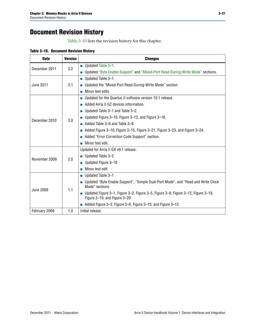
Chapter 3: Memory Blocks in Arria II Devices 3–27Document Revision History
Document Revision HistoryTable 3–10 lists the revision history for this chapter.
Table 3–10. Document Revision History
Date Version Changes
December 2011 3.2■ Updated Table 3–1.
■ Updated “Byte Enable Support” and “Mixed-Port Read-During-Write Mode” sections.
June 2011 3.1
■ Updated Table 3–1.
■ Updated the “Mixed-Port Read-During-Write Mode” section.
■ Minor text edits.
December 2010 3.0
■ Updated for the Quartus II software version 10.1 release.
■ Added Arria II GZ devices information.
■ Updated Table 3–1 and Table 3–2.
■ Updated Figure 3–10, Figure 3–12, and Figure 3–16.
■ Added Table 3–6 and Table 3–8.
■ Added Figure 3–10, Figure 3–15, Figure 3–21, Figure 3–23, and Figure 3–24.
■ Added “Error Correction Code Support” section.
■ Minor text edit.
November 2009 2.0
Updated for Arria II GX v9.1 release:
■ Updated Table 3–2
■ Updated Figure 3–16
■ Minor text edit
June 2009 1.1
■ Updated Table 3–1
■ Updated “Byte Enable Support”, “Simple Dual-Port Mode”, and “Read and Write Clock Mode” sections
■ Updated Figure 3–1, Figure 3–2, Figure 3–5, Figure 3–9, Figure 3–12, Figure 3–18, Figure 3–19, and Figure 3–20
■ Added Figure 3–2, Figure 3–6, Figure 3–10, and Figure 3–13
February 2009 1.0 Initial release
December 2011 Altera Corporation Arria II Device Handbook Volume 1: Device Interfaces and Integration

3–28 Chapter 3: Memory Blocks in Arria II DevicesDocument Revision History
Arria II Device Handbook Volume 1: Device Interfaces and Integration December 2011 Altera Corporation


![,gggzzgzZZZzZeeee$$$ŠŠŠŠââââ]]]]gggg@@@@***ÔÔÔÔ}}FFFF,,,gggg · ,gggzzgzZZZzZeeee$$$ŠŠŠŠââââ]]]]gggg@@@@***ÔÔÔÔ}}}FFFF,,,gggg](https://img.pdfslide.tips/doc/110x75/5b7724c57f8b9ad3338c84a3/gggzzgzzzzzzeeeessssaaaaggggooooffffgggg-gggzzgzzzzzzeeeessssaaaaggggooooffffgggg.jpg)