Embed Size (px)
Citation preview

3D IC Test through
Power Line Methodology
Alberto Pagani

Outline
• Power Line Communication (PLC) approach
• 2D Test architecture through PLC
• Advantages
• Methodology
• Feasibility Study
• Rx test chip for digital signal on power line
• DUT testing reliability
• 3D Test architecture through PLC
• Methodology
• Test procedure
• Advantages
• Conclusions
2

Power Line Communication (PLC) approach 3
… 3D systems are numerous
A house is a good example of 3D architecture
3D Integrated Circuits are well known … WafersWafers
3D Chip
3D Options

4
1st floor
Ground
floor
flat
flat
flat
flat
roof
Mixer + amplifier
Power supply
Our proposal is to apply the same
concept to 3D IC wafer testing
In TV antenna systems, RF signals and
DC power supplies are superposed on
the same coaxial cable
Power Line Communication (PLC) approach

2D Test architecture through PLC Advantages 5
Main advantages of 2D test architecture :
• Significant reduction of probe card complexity due to low number of probes
(best case only two probes)
• Significant reduction of pad damage
• Pad area reduction
• Possibility to
• Analyze customer returns
• Test IC in the final application
• Facilitates in system programming
DUT DUT
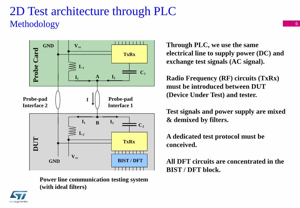
6
Through PLC, we use the same
electrical line to supply power (DC) and
exchange test signals (AC signal).
Radio Frequency (RF) circuits (TxRx)
must be introduced between DUT
(Device Under Test) and tester.
Test signals and power supply are mixed
& demixed by filters.
A dedicated test protocol must be
conceived.
All DFT circuits are concentrated in the
BIST / DFT block.
TxRx
BIST / DFT
V cc
L 1
GND
GND
Pro
be
Card
D
UT
Probe-pad
Interface 2
C 1
C 2
L 2
TxRx
V cc
I
I 1
I 1 I 2
I 2 A
B
Power line communication testing system
(with ideal filters)
2D Test architecture through PLC Methodology
Probe-pad
Interface 1

7
RXCC
CPADOUT
SRESET
Vmin
Vmax Vmax
α β
α β
PRECHARGE CIRCUIT
COMPARATORIN
The figure below represents design architecture of the capacitive Rx.
Rx works in asynchronous mode, switching when a signal edge transition is detected.
A more detailed paper will be submitted for a future IEEE conference.
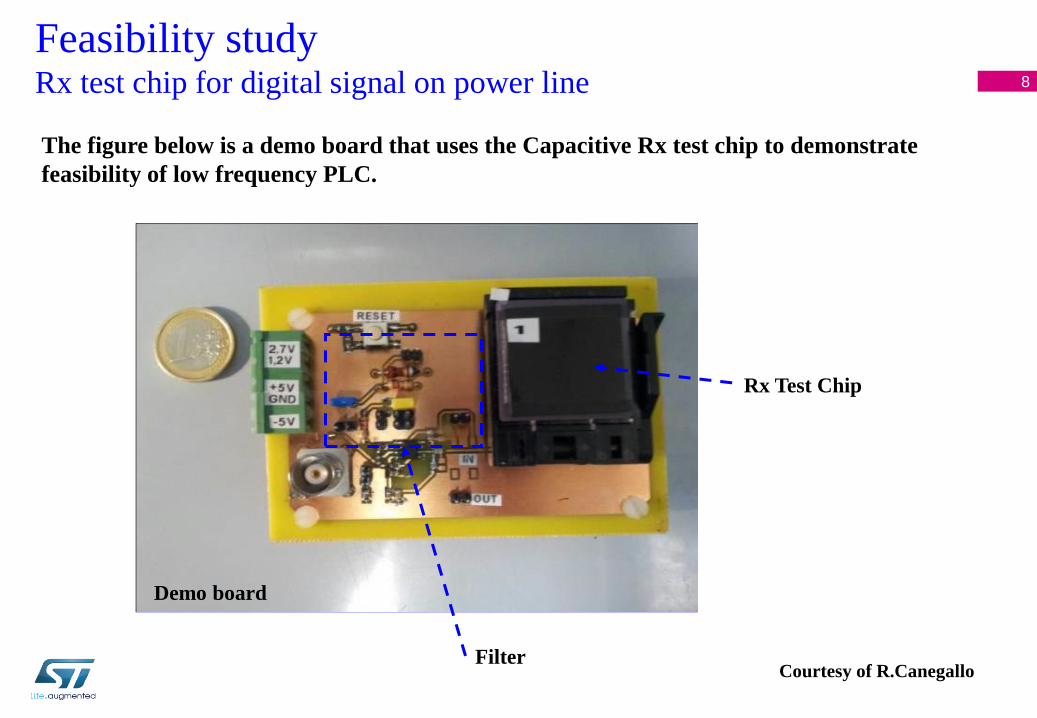
Feasibility study Rx test chip for digital signal on power line
Courtesy of R.Canegallo
8
Rx Test Chip
Filter
Demo board
The figure below is a demo board that uses the Capacitive Rx test chip to demonstrate
feasibility of low frequency PLC.
Courtesy of R.Canegallo
Feasibility study Rx test chip for digital signal on power line

9
Oscilloscope waveforms tested on PCB
Square waveform used for modulation
Input signal
(mix of digital signal + DC power )
Digital signal after
separation
DC power supply after separation
Courtesy of R.Canegallo
Feasibility study Rx test chip for digital signal on power line

Feasibility study DUT testing reliability 10
A commercial VLSI product and production ATE were used to verify that an
additional RF signal superimposed on power line does not affect DUT test results.
DUTATE
Sine wave
generator
Spectrum &
Oscilloscope
No filter was added on DUT power supply lines.
Test bench with a production ATE (Automatic Test
Equipment)
Measurement setup

11
Power supply spectrum of the entire
test program without additional RF
signal (standard test condition)
The test passed demonstrating that an additional RF signal does not affect DUT test results.
It suggests that power supply filters can probably be simplified (avoiding integration of
inductors for example), but this must be evaluated on a product by product basis.
-20dBm -8.9dBm
Feasibility study DUT testing reliability
Power supply spectrum of the entire
test program with additional RF signal
(sine wave is superimposed over DC
power supply)

3D Test architecture through PLC Methodology 12
ICA
ICB
Dedicated
test TSV
signal TSV power TSVpower TSV
ICA
ICB signal TSV power TSVpower TSV
Test signal
Test signal
Dedicated
test TSV
Test signal Test signal
VccVcc GND GNDI/O I/O
The new proposed methodology consists of using power TSVs that connect
several chips in a 3D stack, thus allowing PLC implementation
New proposed test architecture shares
power TSVs for power supply and test
signals
Standard test architectures use
dedicated TSVs for test signals

13
Test stimuli directed to integrated circuit ICA are transmitted for example, using a first
modulation frequency, while test stimuli directed to integrated circuit ICB are transmitted using
a second modulation frequency which is different from the first
Test responses can use other frequencies
Several implementations are possible for example, using CDMA (Code Division Multiple Access)
communication scheme, etc…
ICA
ICB signal TSV power TSVpower TSV
Test signal
Test signal
VccVcc GND GND
3D Test architecture through PLC Test procedure

Main advantages of this new proposed test architecture are:
• Reduction of test pad numbers for 2D pre-bond test and 3D post-bond test
• Simplification of 3D test standardization
• Less constraints at routing design level
• No dedicated TSVs for test signals saving silicon area
• Fault tolerance for power TSV defects due to multiple power TSVs used for each
power supply
14
3D Test architecture through PLC Advantages

15
ICA
ICB signal TSV power TSVpower TSV
Test signal
Test signal
VccVcc
TSV fail
3D Test architecture through PLC Advantages
Architecture is fault tolerant for power TSV defects due to multiple TSVs used for each power
supply (in order to supply right current to each 2D DUT), then there is TSV self-redundancy
that will allow to test 3D DUT also in case of some defective power TSVs.
There are also some considerations to be made when introducing a TxRx and testing protocol.
A probable compromise can be found between:
- TxRx silicon area and area saved by avoiding test TSVs
- TxRx complexity and testing requirements
In any case, different power supplies can be present in 3D DUT, thus simplifying TxRx.

• We demonstrated the feasibility of 2D Test architecture through power line
communication.
• We proposed new methodology for 2D (pre-bond) and 3D (mid-bond & post-
bond) testing through power line communication architecture and related
advantages to 3D testing.
• This has been a research project up till now and we need a customer to develop
and apply it to a product.
16
Conclusions
Thank you!