Embed Size (px)
Citation preview
Matsuzawa& Okada Lab.
A 60GHz CMOS Power Amplifier Using Varactor Cross-Coupling
Neutralization with Adaptive Bias
Ryo Minami,Kota Matsushita, Hiroki Asada, Kenichi Okada,and Akira Matsuzawa
Tokyo Institute of Technology, Japan

1
Matsuzawa& Okada Lab.2011/12/07
Outline• Background• Capacitor cross-coupling method• Proposed varactor cross-coupling method– Applied capacitor cross-coupling– The optimal capacitance is designed by using
adaptive bias• Measurement result– Power gain– Power added efficiency (PAE)– Power consumption
• Performance comparison• Conclusion

2
Matsuzawa& Okada Lab.
Background
IEEE 802.15.3c・QPSK ⇒ 3.5Gbps/ch・16QAM ⇒ 7.0Gbps/ch
Advantage of 60GHz
High speed wireless communication can be realized without lisence.
Wireless Transmission of uncompressed HDTV
Gbps Wireless Communication
Enable communication distance is short.

3
Matsuzawa& Okada Lab.
A 60GHz wireless transceiver[1], [2]
[1] K. Okada, et al., ISSCC 2011[2] A. Musa, et al., ASSCC 2010
At 60GHz wireless communication
• High output power• High efficiency

4
Matsuzawa& Okada Lab.
Transmission Line
capacitance(0.999 [µF])
inductance(1 [H]) inductance(1 [H])
capacitance(0.999 [µF])
The structure of TL.
Modeland photo.
lumped constantdistributed constant
At 60GHz, the size of component is not negligiblecomparing the wavelength.
DCAC
transmission line is used.

5
Matsuzawa& Okada Lab.•5
MIM Transmission Line
• De-coupling use• Modeling accuracy• Avoiding self-resonance of
parallel-plate capacitors
0123456789
10
0 10 20 30 40 50 60 70Frequency [GHz]
Z0[O
hm]
MeasuredModel
GND
MIM TL
GND
GND
GND
TL
MIM capacitor
MIM transmission line
50Ω transmission line
[3] T. Suzuki, et al., ISSCC 2008
6
Matsuzawa& Okada Lab.
0
5
10
15
20
25
30
0 10 20 30 40 50 60 70 80 90 100 110
Max
imum
avai
labl
ega
in[d
B]
Frequency [GHz]
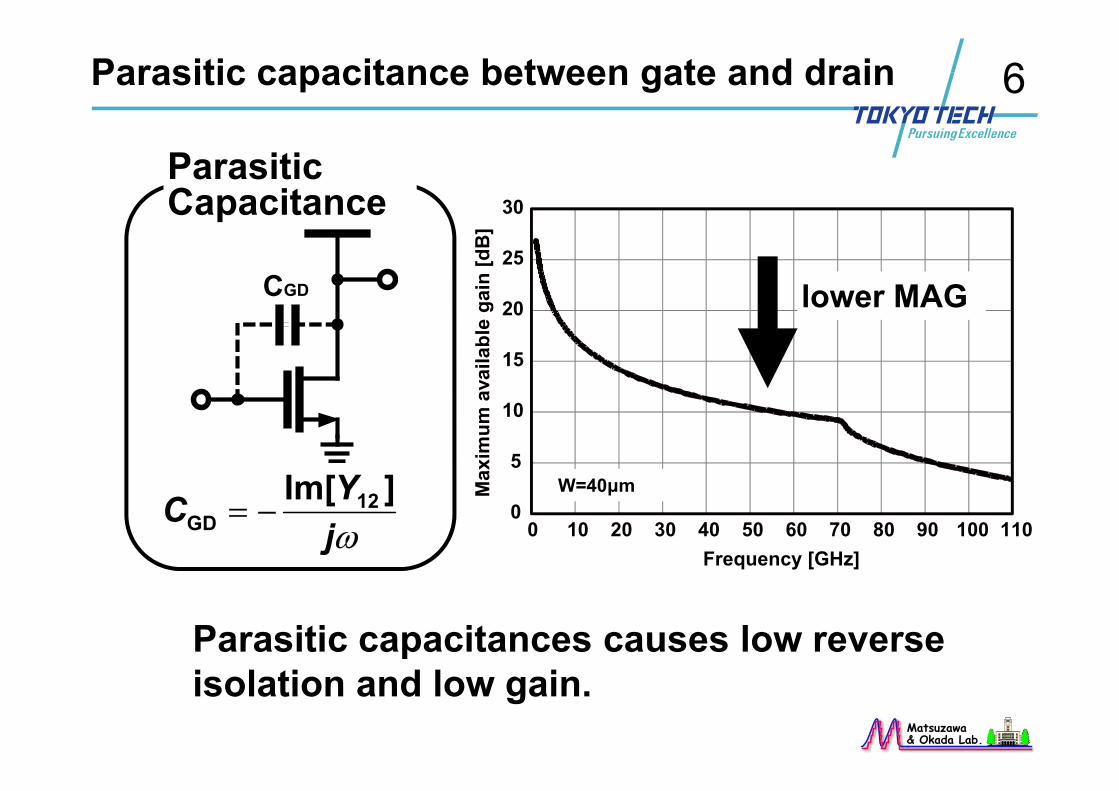
Parasitic capacitance between gate and drain
Parasitic capacitances causes low reverse isolation and low gain.
Parasitic Capacitance
lower MAG
ωjYC ]Im[ 12
GD −=W=40µm
CGD

7
Matsuzawa& Okada Lab.
Capacitor cross-coupling[3]
[4] W. L. Chan, et al., ISSCC 2009
IN
OUT
-Cx -Cx
Cx Cx
IN
OUT
Vdd
A cross-coupled capacitor between gate and drain of the opposite-side transistor works as negative capacitor.– The reverse isolation is improved.

8
Matsuzawa& Okada Lab.
Simulation result of CCC
• Stability Factor is improved across entire frequency.• The maximum available gain is
improved about 2dB at 60GHz.
0
5
10
15
20
25
30
MA
G,M
SG[d
B]
Frequency [GHz]
w/ CCCw/o CCC
00.20.40.60.8
11.21.41.61.8
2
0 10 20 30 40 50 60 70 80 90 100 110
Stab
lity
fact
or
Frequency [GHz]
w/ CCCw/o CCC

9
Matsuzawa& Okada Lab.
Simulation result of PAE
0
2
4
6
8
10
12
14
-10 -8 -6 -4 -2 0 2 4 6 8 10 12 14 16
PAE
[%]
Input power [dBm]
Larger C
Smaller C
• The optimal capacitance is depended on the input power.
Varactor is used as a cross coupled capacitor
• Smaller input power Larger C than Cx is better • Larger input power Smaller C than Cx is better
10
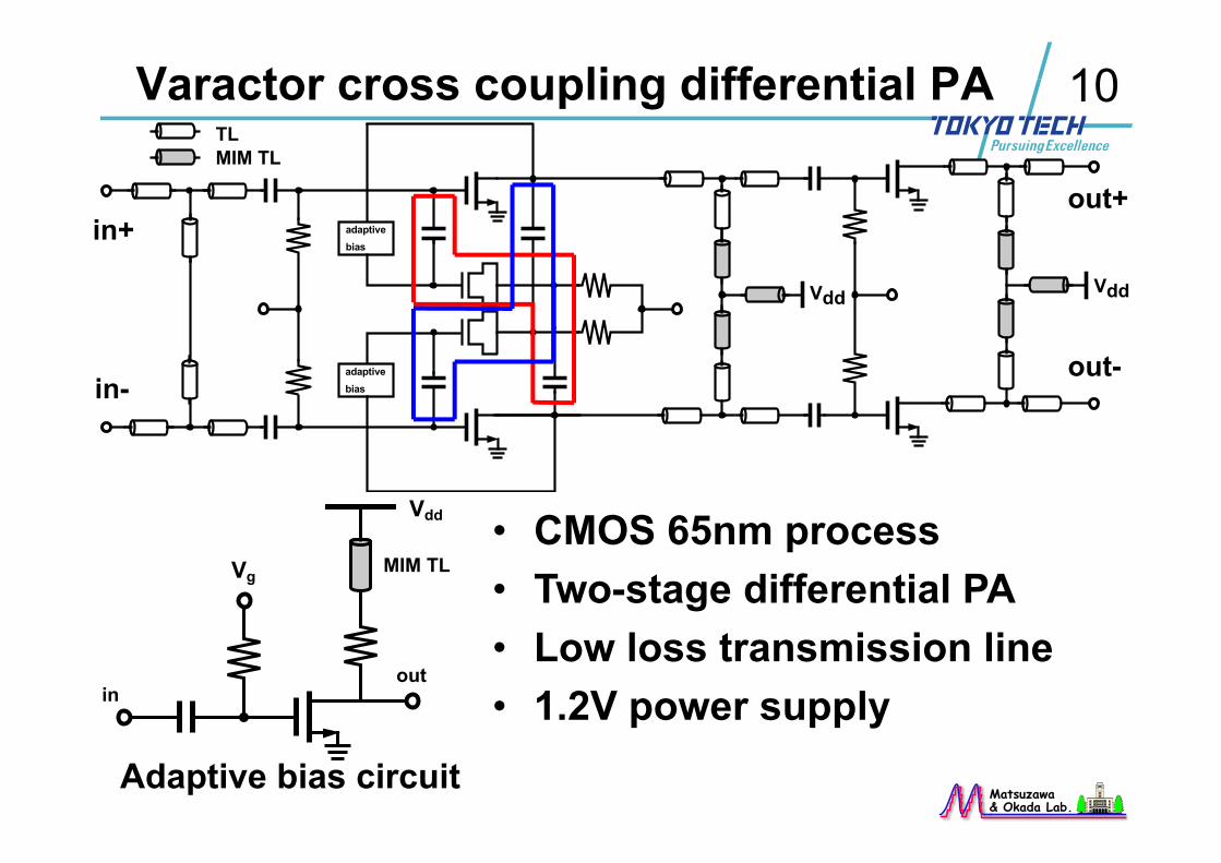
Matsuzawa& Okada Lab.
adaptivebias
adaptivebias
TLMIM TL
Vdd Vdd
in+
in-
out+
out-
Varactor cross coupling differential PA
Adaptive bias circuit
• CMOS 65nm process• Two-stage differential PA• Low loss transmission line • 1.2V power supplyin
out
MIM TLVg
Vdd

11
Matsuzawa& Okada Lab.
Simulation result of varactor
0
0.1
0.2
0.3
0.4
0.5
0.6
0.7
0.8
0.9
1
10
15
20
25
30
35
40
-10 -8 -6 -4 -2 0 2 4 6 8 10
Volta
ge[V
]
Cap
acita
nce
[fF]
Input power [dBm]
VaractorcapacitanceAdaptivebias
• Optimal capacitance is realized by varying the bias of varactor using feedback of input power.

12
Matsuzawa& Okada Lab.
Die photo

13
Matsuzawa& Okada Lab.
Measurement result (small signal)
About 10GHz frequency error is generated between simulation and measurement.
The accuracy of models were not good.
• Sim.(old) shows the result of using old models.• Sim.(new) shows the result of using update models.
-14
-12
-10
-8
-6
-4
-2
0
30 35 40 45 50 55 60 65 70
S 11
[dB
]
Frequency [GHz]
Sim. (old)
Sim. (new)
Meas.
-35
-30
-25
-20
-15
-10
-5
0
30 35 40 45 50 55 60 65 70
S 22
[dB
]
Frequency [GHz]
Sim. (old)
Sim. (new)
Meas.

14
Matsuzawa& Okada Lab.
Measurement result (large signal)
Gain: 12.1dBPAE at P1dB: 7.7%Peak PAE: 12.5%
Psat: 12.2dBmPDC: 86mWVDD: 1.2V
0
2
4
6
8
10
12
14
16
-10
-5
0
5
10
15
-30 -25 -20 -15 -10 -5 0 5 10
PAE
[%]
Out
putp
ower
[dB
m],
Gai
n[d
B]
Input power [dBm]
Output powerGainPAE

15
Matsuzawa& Okada Lab.
Performance comparisonTech. Gain
[dB]P1dB
[dBm]Psat
[dBm]PAE@P1dB
[dBm]Power [mW] VDD[V]
ISSCC 2008[5] 65nm 5.5 9 12.3 6 - 1.0
ISSCC 2009[4] 65nm 16 2.5 11.5 4.5 43.5 1.0
ISSCC 2010[6] 65nm 14.3 11 16.6 1.3 732 1.2
ISSCC 2010[7] 65nm 19.2 15.4 17.7 7 480 1.0
ISSCC 2011[8] 65nm 20.3 15 18.6 6.3 72 1.0
This Work 65nm 12.1 9.5 12.2 7.7 86 1.2
Very good PAE at P1dB is realized.[4] W. L. Chan, et al., ISSCC 2009[5] D. Chowdhury, et al., ISSCC 2008
[6] B. Martineau, et al., ISSCC 2010[7] J. Lai, et al., ISSCC 2010
[8] J. Chen, et al., ISSCC 2011

16
Matsuzawa& Okada Lab.
Conclusion
• A 60GHz varactor cross coupled 2-stage differential power amplifier is implemented by using CMOS 65nm process.
• Very good power added efficiency (PAE) at 1-dB power compression point is realized in proposed CMOS power amplifier.