Embed Size (px)
Citation preview
A 7T/14T Dependable SRAM and Its Array Structure to Avoid Half Selection
Hidehiro Fujiwara, Shunsuke Okumura, Yusuke Iguchi, Hiroki Noguchi, Hiroshi Kawaguchi, and Masahiko Yoshimoto
Graduate school of Engineering Kobe University, Kobe, Japan [email protected]
Abstract
We propose a novel dependable SRAM with 7T cells and their array structure that avoids a half-selection problem. In addition, we introduce a new concept, “quality of a bit (QoB)” for it. The dependable SRAM has three modes (normal mode, high-speed mode, and dependable mode), and dynamically scales its reliability and speed by combining two memory cells for one-bit information (i.e. 14T/bit). Monte Carlo simulation demonstrates that, in a 65-nm process technology, the minimum voltages in read and write operations are improved by 0.20V and 0.26V, respectively, with a bit error rate of 10-8 kept. The cell area overhead is 11%, compared to the conventional 6T cell in the normal mode. 1. Introduction
Recently, they have paid attention to dependable computing systems, as silicon LSIs support massive infrastructure in society. However, the advanced process technology tends to cause accidental errors like a soft error and negative bias temperature instability (NBTI), more frequently. In addition, there might be some errors left in a design, manufacturing, or test phase. It is supposed to be almost impossible to perfectly eliminate these human-induced errors in a future complicated LSI. That is, a product will be shipped with some errors, and accidentally malfunction. We no longer expect error-free LSIs with sufficient operating margins.
Since reliability is varied with operating conditions (speed, supply voltage, temperature, and even altitude corresponding to a soft error), it is desirable to dynamically improve the reliability on worse conditions. Furthermore, required reliability depends on an application software, which indicates that the reliability should be changed in accordance with the application.
Considering this background, we propose an SRAM that can dynamically control its reliability. An SRAM has recently dominated operating margins of a chip due to a large number of transistors [1-7]. Other than the reliability, the proposed SRAM also achieves fast operation and/or low-poer operation, with the same reliability kept as the conventional SRAM. Namely, the proposed SRAM can change quality of its information, in terms of reliability, speed, and/or power.
In the next section, we describe the overview of the proposed SRAM. In Section 3, we propose a novel 7T memory cells to dynamically improve the quality of information, and introduce a new concept called “quality of a bit” (QoB). In Section 4, we discuss the reliability of the proposed memory cell, from view points of a cell current and a bit error rate. In Section 5, we mention the new cell array structure for the proposed SRAM to avoid the half-selection problem. The final section summarizes this paper. 2. Dependable SRAM: Overview
Operating conditions affect reliability of an SRAM, while the reliability depends on an application software that uses the SRAM. An encryption program and a screen saver program demand different levels of reliability. This means that the reliability is changed by the operating conditions, and is dependent on the application.
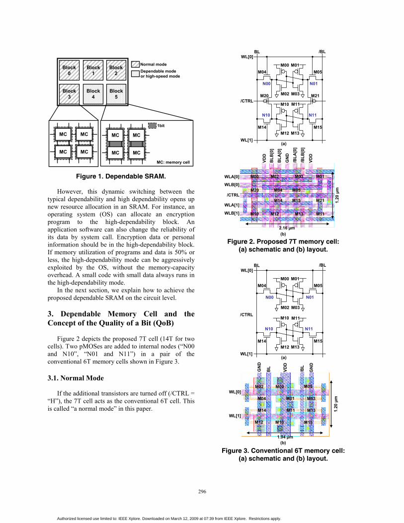
In our proposed dependable SRAM, reliability and speed of an SRAM can be dynamically changed on a block-by-block basis, as illustrated in Figure 1. In the normal mode (Blocks 0-3), assignment is as usual as one memory cell has one bit. On the other hand, in the dependable or high-speed mode (Blocks 4 and 5), one-bit information is stored in two memory cells by combining a pair of memory cells. This mechanism selectively realizes the high reliability or high speed, while the memory capacity becomes a half in these modes.
2009 22nd International Conference on VLSI Design
1063-9667/09 $25.00 © 2009 IEEE
DOI 10.1109/VLSI.Design.2009.54
295
Authorized licensed use limited to: IEEE Xplore. Downloaded on March 12, 2009 at 07:39 from IEEE Xplore. Restrictions apply.
MC MC
MC MC
1bit
Normal modeDependable modeor high-speed mode
MC MC
MC MC
Block 0
Block 1
Block 2
Block 3
Block 4
Block 5
MC: memory cell
Figure 1. Dependable SRAM.
However, this dynamic switching between the
typical dependability and high dependability opens up new resource allocation in an SRAM. For instance, an operating system (OS) can allocate an encryption program to the high-dependability block. An application software can also change the reliability of its data by system call. Encryption data or personal information should be in the high-dependability block. If memory utilization of programs and data is 50% or less, the high-dependability mode can be aggressively exploited by the OS, without the memory-capacity overhead. A small code with small data always runs in the high-dependability mode.
In the next section, we explain how to achieve the proposed dependable SRAM on the circuit level.
3. Dependable Memory Cell and the Concept of the Quality of a Bit (QoB)
Figure 2 depicts the proposed 7T cell (14T for two cells). Two pMOSes are added to internal nodes (“N00 and N10”, “N01 and N11”) in a pair of the conventional 6T memory cells shown in Figure 3. 3.1. Normal Mode
If the additional transistors are turned off (/CTRL =
“H”), the 7T cell acts as the conventional 6T cell. This is called “a normal mode” in this paper.
WL[0]
WL[1]
BL /BL
/CTRL
N00 N01
N11N10
M00 M01
M02 M03
M04 M05
M10 M11
M12 M13M14 M15
M20 M21
(a)
WLA[0]
WLB[0]
WLB[1]
WLA[1]
/CTRL
VDD
BLB
[0]
BLA
[0]
GN
D
/BLA
[0]
/BLB
[0]
VDD
(b)
M01M00 M02 M03
M04 M05
M15M14
M10 M11
M20
M12 M13
1.20
µm
2.16 µm
M21
Figure 2. Proposed 7T memory cell:
(a) schematic and (b) layout.
WL[0]
WL[1]
BL /BL
/CTRL
N00 N01
N11N10
M00 M01
M02 M03
M04 M05
M10 M11
M12 M13M14 M15
(a)
M00M02
M01 M03M04
M05
M11
M10M12
M13
M15
M14
WL[0]
WL[1]
GN
D
BL
VDD
/BL
GN
D
1.20
µm
1.94 µm(b)
Figure 3. Conventional 6T memory cell: (a) schematic and (b) layout.
296
Authorized licensed use limited to: IEEE Xplore. Downloaded on March 12, 2009 at 07:39 from IEEE Xplore. Restrictions apply.
3.2. High-Speed Mode Alternatively, if the additional transistors are turned
on (/CTRL = “L”), and the internal nodes are shared by the pair of memory cell. The high speed is achieved when both WL[0] and WL[1] are driven, which enables a faster readout.
3.3. Dependable Mode
The most significant usage of the proposed 7T
memory cell is the dependable mode. The additional transistors are activated, but either WL[0] or WL[1] is asserted. Thus, only one word line is asserted. By doing so, a larger β ratio and static noise margin can be obtained because the dependable mode has two access transistor but four drive transistors in a memory cell.
3.4. Quality of a Bit
As mentioned above, we have three modes in the proposed 7T memory cell. Table 1 summarizes these modes. In the normal mode, one-bit datum is stored in one memory cell, which is the most area-efficient. In the high-speed mode and dependable mode, one-bit datum is stored in two memory cells although the quality of the information is different from the typical mode. The “higher-speed” or “more dependable” information can be obtained. We call this concept “quality of a bit (QoB)”. The quality of the information is scalable in our proposed memory cell.
Table 1. Three modes in 7T memory cell.
“L” (on)12 (14T/bit)Dependable
“L” (on)22 (14T/bit)High-speed
“H” (off)11 (7T/bit)Normal
/CTRL# of WL drives# of MCs comprising 1 bit
4. Dependability Simulation
In this section, we discuss the dependability of our proposed memory cell from view points of a cell current and a bit error rate. 4.1. Cell Current
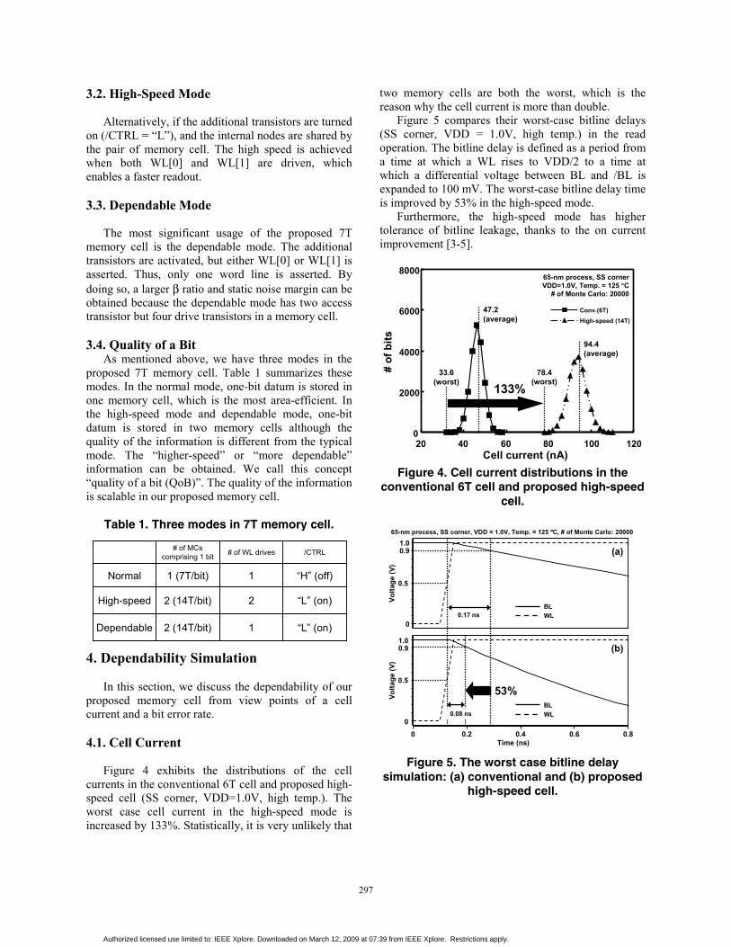
Figure 4 exhibits the distributions of the cell currents in the conventional 6T cell and proposed high-speed cell (SS corner, VDD=1.0V, high temp.). The worst case cell current in the high-speed mode is increased by 133%. Statistically, it is very unlikely that
two memory cells are both the worst, which is the reason why the cell current is more than double.
Figure 5 compares their worst-case bitline delays (SS corner, VDD = 1.0V, high temp.) in the read operation. The bitline delay is defined as a period from a time at which a WL rises to VDD/2 to a time at which a differential voltage between BL and /BL is expanded to 100 mV. The worst-case bitline delay time is improved by 53% in the high-speed mode.
Furthermore, the high-speed mode has higher tolerance of bitline leakage, thanks to the on current improvement [3-5].
0
2000
4000
6000
8000
20 40 60 80 100 120
65-nm process, SS cornerVDD=1.0V, Temp. = 125 °C
# of Monte Carlo: 20000
33.6(worst)
78.4(worst)
133%
47.2(average)
94.4(average)
Conv.(6T)High-speed (14T)
Cell current (nA)
# of
bits
Figure 4. Cell current distributions in the
conventional 6T cell and proposed high-speed cell.
0
1.00.9
0
1.00.9
0 0.2 0.4 0.6 0.8Time (ns)
Volta
ge (V
)Vo
ltage
(V)
0.5
0.5
0.08 ns
0.17 ns
53%BLWL
BLWL
(a)
(b)
65-nm process, SS corner, VDD = 1.0V, Temp. = 125 ºC, # of Monte Carlo: 20000
Figure 5. The worst case bitline delay
simulation: (a) conventional and (b) proposed high-speed cell.
297
Authorized licensed use limited to: IEEE Xplore. Downloaded on March 12, 2009 at 07:39 from IEEE Xplore. Restrictions apply.
4.2. Bit Error Rate (BER)
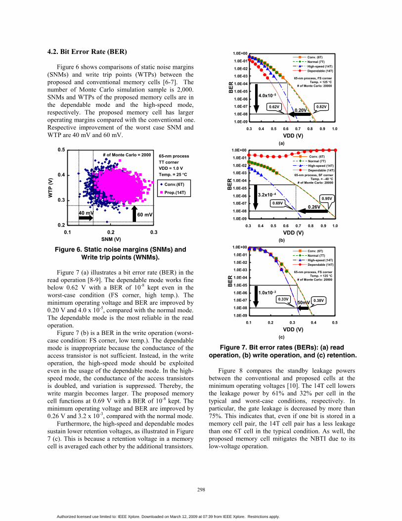
Figure 6 shows comparisons of static noise margins (SNMs) and write trip points (WTPs) between the proposed and conventional memory cells [6-7]. The number of Monte Carlo simulation sample is 2,000. SNMs and WTPs of the proposed memory cells are in the dependable mode and the high-speed mode, respectively. The proposed memory cell has larger operating margins compared with the conventional one. Respective improvement of the worst case SNM and WTP are 40 mV and 60 mV.
0.2
0.3
0.4
0.5
0.1 0.2 0.3SNM (V)
WTP
(V)
Conv.(6T)
Prop.(14T)
65-nm processTT cornerVDD = 1.0 VTemp. = 25 °C
40 mV 60 mV
# of Monte Carlo = 2000
Figure 6. Static noise margins (SNMs) and
Write trip points (WNMs).
Figure 7 (a) illustrates a bit error rate (BER) in the read operation [8-9]. The dependable mode works fine below 0.62 V with a BER of 10-8 kept even in the worst-case condition (FS corner, high temp.). The minimum operating voltage and BER are improved by 0.20 V and 4.0 x 10⁻⁵, compared with the normal mode. The dependable mode is the most reliable in the read operation.
Figure 7 (b) is a BER in the write operation (worst-case condition: FS corner, low temp.). The dependable mode is inappropriate because the conductance of the access transistor is not sufficient. Instead, in the write operation, the high-speed mode should be exploited even in the usage of the dependable mode. In the high-speed mode, the conductance of the access transistors is doubled, and variation is suppressed. Thereby, the write margin becomes larger. The proposed memory cell functions at 0.69 V with a BER of 10-8 kept. The minimum operating voltage and BER are improved by 0.26 V and 3.2 x 10⁻³, compared with the normal mode.
Furthermore, the high-speed and dependable modes sustain lower retention voltages, as illustrated in Figure 7 (c). This is because a retention voltage in a memory cell is averaged each other by the additional transistors.
1.0E-09
1.0E-08
1.0E-07
1.0E-06
1.0E-05
1.0E-04
1.0E-03
1.0E-02
1.0E-01
1.0E+00
0.3 0.4 0.5 0.6 0.7 0.8 0.9 1.0
VDD (V)
BER
65-nm process, FS cornerTemp. = 125 °C
# of Monte Carlo: 20000
0.62V
4.0x10⁻⁵
0.82V0.20V
(a)
Conv. (6T)Normal (7T)High-speed (14T)Dependable (14T)
(b)
1.0E-09
1.0E-08
1.0E-07
1.0E-06
1.0E-05
1.0E-04
1.0E-03
1.0E-02
1.0E-01
1.0E+00
0.3 0.4 0.5 0.6 0.7 0.8 0.9 1.0
VDD (V)B
ER
0.69V0.95V
0.26V
3.2x10⁻⁴
65-nm process, SF cornerTemp. = −40 °C
# of Monte Carlo: 20000
Conv. (6T)Normal (7T)High-speed (14T)Dependable (14T)
1.0E-09
1.0E-08
1.0E-07
1.0E-06
1.0E-05
1.0E-04
1.0E-03
1.0E-02
1.0E-01
1.0E+00
BER
VDD (V)0.1 0.2 0.3 0.4 0.5
65-nm process, FS cornerTemp. = 125 °C
# of Monte Carlo: 20000
(c)
0.33V 0.38V50mV
1.0x10⁻³
Conv. (6T)Normal (7T)High-speed (14T)Dependable (14T)
Figure 7. Bit error rates (BERs): (a) read
operation, (b) write operation, and (c) retention.
Figure 8 compares the standby leakage powers between the conventional and proposed cells at the minimum operating voltages [10]. The 14T cell lowers the leakage power by 61% and 32% per cell in the typical and worst-case conditions, respectively. In particular, the gate leakage is decreased by more than 75%. This indicates that, even if one bit is stored in a memory cell pair, the 14T cell pair has a less leakage than one 6T cell in the typical condition. As well, the proposed memory cell mitigates the NBTI due to its low-voltage operation.
298
Authorized licensed use limited to: IEEE Xplore. Downloaded on March 12, 2009 at 07:39 from IEEE Xplore. Restrictions apply.
0
1
2
6T cell(VDD = 0.95V)
14T cell(VDD = 0.69V)
Stan
dby
leak
age
pow
er (n
W/c
ell)
(a)
6T cell(VDD = 0.95V)
14T cell(VDD = 0.69V)
(b)
65-nm process , TT corner Temp. = 25 °C
61%
Gate leakage Subthreshold leakage
0
10
20
30
40
50
32%
65-nm process , FF cornerTemp. = 125 °C
Stan
dby
leak
age
pow
er (n
W/c
ell)
Figure 8. Standby leakage power per cell: (a)
TT corner, 25 °Cand (b) FF corner, 125 °C.
1.0E-09
1.0E-081.0E-07
1.0E-061.0E-05
1.0E-041.0E-03
1.0E-021.0E-01
1.0E+00
0.3 0.4 0.5 0.6 0.7 0.8 0.9 1
VDD (V)
BER
65-nm process, FS corner, Temp. = 125 °C, # of Monte Carlo: 20000
Conv. (6T)6T with ECC6T with MMRDependable (14TP)
Figure 9. Comparison of BERs among the
conventional methods and 14TP dependable mode.
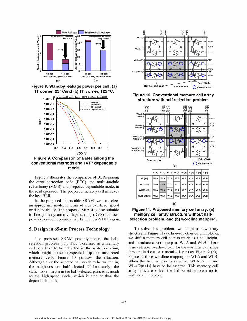
Figure 9 illustrates the comparison of BERs among
the error correction code (ECC), the multi-module redundancy (MMR) and proposed dependable mode, in the read operation. The proposed memory cell achieves the best BER.
In the proposed dependable SRAM, we can select an appropriate mode, in terms of area overhead, speed or dependability. The proposed SRAM is also suitable to fine-grain dynamic voltage scaling (DVS) for low-power operation because it works in a low-VDD region. 5. Design in 65-nm Process Technology
The proposed SRAM possibly incurs the half-selection problem [11]. Two wordlines in a memory cell pair have to be activated in the write operation, which might cause unexpected flips in unselected memory cells. Figure 10 portrays the situation. Although only the selected pair needs to be written in, the neighbors are half-selected. Unfortunately, the static noise margin in the half-selected pairs is as much as the high-speed mode, which is smaller than the dependable mode.
WL[2n]
WL[2n+1]
WL[2(n+1)]
WL[2(n+1)+1]
BL[0
]
/BL[
0]
BL[1
]
/BL[
1]
/BL[
2]
BL[2
]
Selected pairHalf-selected pairs
“H”
“H”
Pair of MCs
On transistor
/CTRL
/CTRL
Figure 10. Conventional memory cell array
structure with half-selection problem
WLA[2n]WLB[2n]
WLA[2n+1]WLB[2n+1]
WLA[2(n+1)]WLB[2(n+1)]
WLA[2(n+1)+1]WLB[2(n+1)+1]
BLB
[0]
BLA
[0]
/BLA
[0]
/BLB
[0]
BLB
[1]
BLA
[1]
/BLA
[1]
/BLB
[1]
/BLA
[2]
/BLB
[2]
BLB
[2]
BLA
[2]
“H”
“H”
Selected pair
(a)
Pair of MCs
On transistor
/CTRL
/CTRL
(b)
WLBWLBWLAWLAWLBWLBWLAWLAWL[2(n+1)+1]
WLBWLBWLBWLBWLAWLAWLAWLAWL[2(n+1)]
WLBWLBWLAWLAWLBWLBWLAWLAWL[2n+1]
WLBWLBWLBWLBWLAWLAWLAWLAWL[2n]
BL[7]BL[6]BL[5]BL[4]BL[3]BL[2]BL[1]BL[0]
Figure 11. Proposed memory cell array: (a) memory cell array structure without half-
selection problem, and (b) wordline mapping.
To solve this problem, we adopt a new array structure in Figure 11 (a). In every other column blocks, we shift a memory cell pair as much as a cell height, and introduce a wordline pair: WLA and WLB. There is no cell area overhead paid for the wordline pair since they are laid out on a metal-4 layer (see Figure 2 (b)). Figure 11 (b) is wordline mapping for WLA and WLB. When the hatched pair is selected, WLA[2n+1] and WLA[2(n+1)] have to be asserted. This memory cell array structure solves the half-select problem up to eight column blocks.
299
Authorized licensed use limited to: IEEE Xplore. Downloaded on March 12, 2009 at 07:39 from IEEE Xplore. Restrictions apply.
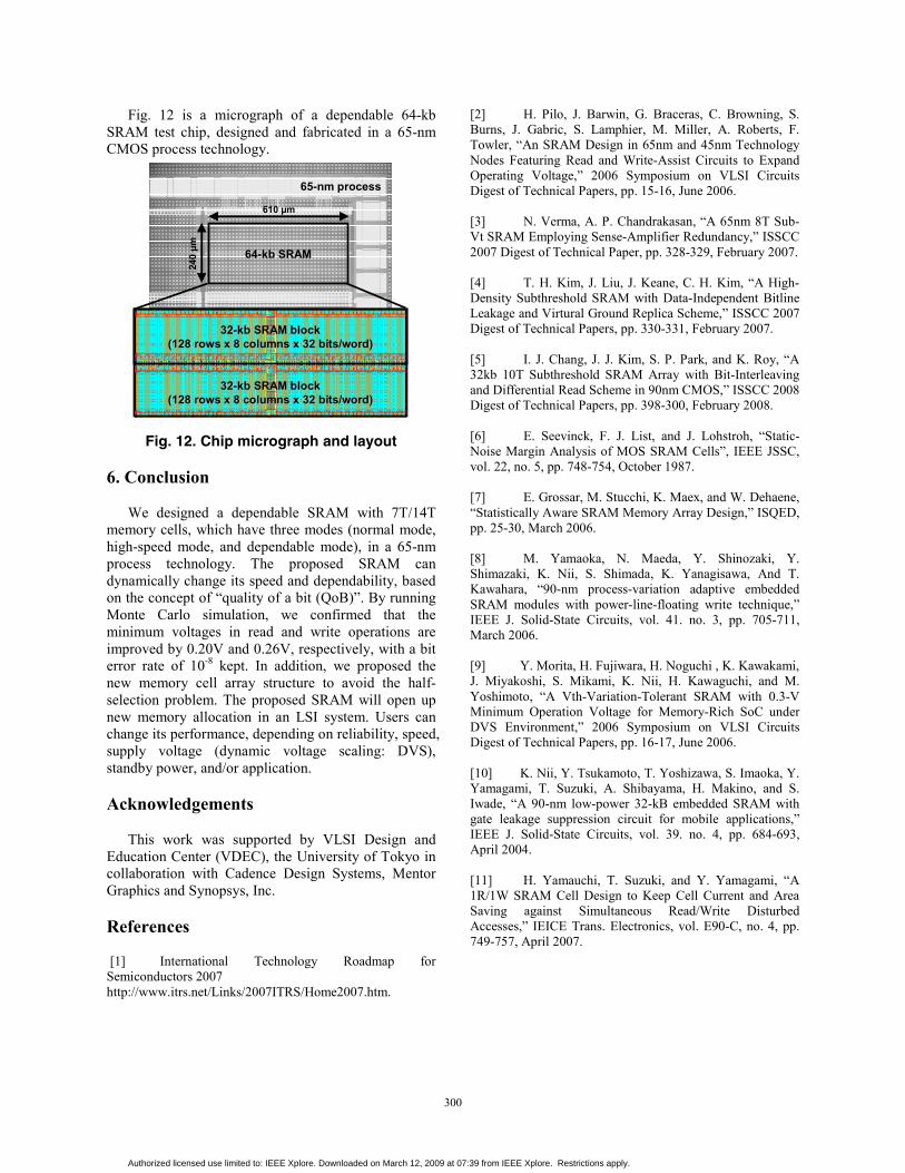
Fig. 12 is a micrograph of a dependable 64-kb SRAM test chip, designed and fabricated in a 65-nm CMOS process technology.
3232--kb SRAM blockkb SRAM block(128 rows x 8 columns x 32 bits/word)(128 rows x 8 columns x 32 bits/word)
6464--kb SRAMkb SRAM
3232--kb SRAM blockkb SRAM block(128 rows x 8 columns x 32 bits/word)(128 rows x 8 columns x 32 bits/word)
610 µm
240
µm65-nm process
Fig. 12. Chip micrograph and layout
6. Conclusion
We designed a dependable SRAM with 7T/14T memory cells, which have three modes (normal mode, high-speed mode, and dependable mode), in a 65-nm process technology. The proposed SRAM can dynamically change its speed and dependability, based on the concept of “quality of a bit (QoB)”. By running Monte Carlo simulation, we confirmed that the minimum voltages in read and write operations are improved by 0.20V and 0.26V, respectively, with a bit error rate of 10-8 kept. In addition, we proposed the new memory cell array structure to avoid the half-selection problem. The proposed SRAM will open up new memory allocation in an LSI system. Users can change its performance, depending on reliability, speed, supply voltage (dynamic voltage scaling: DVS), standby power, and/or application.
Acknowledgements
This work was supported by VLSI Design and Education Center (VDEC), the University of Tokyo in collaboration with Cadence Design Systems, Mentor Graphics and Synopsys, Inc.
References [1] International Technology Roadmap for Semiconductors 2007 http://www.itrs.net/Links/2007ITRS/Home2007.htm.
[2] H. Pilo, J. Barwin, G. Braceras, C. Browning, S. Burns, J. Gabric, S. Lamphier, M. Miller, A. Roberts, F. Towler, “An SRAM Design in 65nm and 45nm Technology Nodes Featuring Read and Write-Assist Circuits to Expand Operating Voltage,” 2006 Symposium on VLSI Circuits Digest of Technical Papers, pp. 15-16, June 2006. [3] N. Verma, A. P. Chandrakasan, “A 65nm 8T Sub-Vt SRAM Employing Sense-Amplifier Redundancy,” ISSCC 2007 Digest of Technical Paper, pp. 328-329, February 2007. [4] T. H. Kim, J. Liu, J. Keane, C. H. Kim, “A High-Density Subthreshold SRAM with Data-Independent Bitline Leakage and Virtural Ground Replica Scheme,” ISSCC 2007 Digest of Technical Papers, pp. 330-331, February 2007. [5] I. J. Chang, J. J. Kim, S. P. Park, and K. Roy, “A 32kb 10T Subthreshold SRAM Array with Bit-Interleaving and Differential Read Scheme in 90nm CMOS,” ISSCC 2008 Digest of Technical Papers, pp. 398-300, February 2008. [6] E. Seevinck, F. J. List, and J. Lohstroh, “Static-Noise Margin Analysis of MOS SRAM Cells”, IEEE JSSC, vol. 22, no. 5, pp. 748-754, October 1987. [7] E. Grossar, M. Stucchi, K. Maex, and W. Dehaene, “Statistically Aware SRAM Memory Array Design,” ISQED, pp. 25-30, March 2006. [8] M. Yamaoka, N. Maeda, Y. Shinozaki, Y. Shimazaki, K. Nii, S. Shimada, K. Yanagisawa, And T. Kawahara, “90-nm process-variation adaptive embedded SRAM modules with power-line-floating write technique,” IEEE J. Solid-State Circuits, vol. 41. no. 3, pp. 705-711, March 2006. [9] Y. Morita, H. Fujiwara, H. Noguchi , K. Kawakami, J. Miyakoshi, S. Mikami, K. Nii, H. Kawaguchi, and M. Yoshimoto, “A Vth-Variation-Tolerant SRAM with 0.3-V Minimum Operation Voltage for Memory-Rich SoC under DVS Environment,” 2006 Symposium on VLSI Circuits Digest of Technical Papers, pp. 16-17, June 2006. [10] K. Nii, Y. Tsukamoto, T. Yoshizawa, S. Imaoka, Y. Yamagami, T. Suzuki, A. Shibayama, H. Makino, and S. Iwade, “A 90-nm low-power 32-kB embedded SRAM with gate leakage suppression circuit for mobile applications,” IEEE J. Solid-State Circuits, vol. 39. no. 4, pp. 684-693, April 2004. [11] H. Yamauchi, T. Suzuki, and Y. Yamagami, “A 1R/1W SRAM Cell Design to Keep Cell Current and Area Saving against Simultaneous Read/Write Disturbed Accesses,” IEICE Trans. Electronics, vol. E90-C, no. 4, pp. 749-757, April 2007.
300
Authorized licensed use limited to: IEEE Xplore. Downloaded on March 12, 2009 at 07:39 from IEEE Xplore. Restrictions apply.


![Dependable Non-Volatile Memory - TU Braunschweig€¦ · Dependable Non-Volatile Memory SYSTOR ’18, June 4–7, 2018, HAIFA, Israel of 106 up to 1010 operations [6, 19, 25]. Once](https://img.pdfslide.tips/doc/110x75/605dd1c8b72c9c6f905bfd6b/dependable-non-volatile-memory-tu-braunschweig-dependable-non-volatile-memory.jpg)


![WJ]7T= - ee-ko.com](https://img.pdfslide.tips/doc/110x75/61d6575594e9aa06f1700b53/wj7t-ee-kocom.jpg)