Embed Size (px)
Citation preview
PR
IFY
SG
OL
BA
NG
OR
/ B
AN
GO
R U
NIV
ER
SIT
Y
A high-yield vacuum-evaporation-based R2R-compatible fabrication routefor organic electronic circuitsPatchett, E.R.; Patchett, E.F.; Williams, A.; Ding, Z.; Abbas, G.; Assender, H.E.;Morrison, J.J.; Yeates, S.G.; Taylor, D.M.
Organic Electronics
DOI:10.1016/j.orgel.2014.03.043
Published: 24/04/2014
Publisher's PDF, also known as Version of record
Cyswllt i'r cyhoeddiad / Link to publication
Dyfyniad o'r fersiwn a gyhoeddwyd / Citation for published version (APA):Patchett, E. R., Patchett, E. F., Williams, A., Ding, Z., Abbas, G., Assender, H. E., Morrison, J.J., Yeates, S. G., & Taylor, D. M. (2014). A high-yield vacuum-evaporation-based R2R-compatible fabrication route for organic electronic circuits. Organic Electronics, 15(7), 1493-1502. https://doi.org/10.1016/j.orgel.2014.03.043
Hawliau Cyffredinol / General rightsCopyright and moral rights for the publications made accessible in the public portal are retained by the authors and/orother copyright owners and it is a condition of accessing publications that users recognise and abide by the legalrequirements associated with these rights.
• Users may download and print one copy of any publication from the public portal for the purpose of privatestudy or research. • You may not further distribute the material or use it for any profit-making activity or commercial gain • You may freely distribute the URL identifying the publication in the public portal ?
Take down policyIf you believe that this document breaches copyright please contact us providing details, and we will remove access tothe work immediately and investigate your claim.
17. Mar. 2022
Organic Electronics 15 (2014) 1493–1502
Contents lists available at ScienceDirect
Organic Electronics
journal homepage: www.elsevier .com/locate /orgel
A high-yield vacuum-evaporation-based R2R-compatiblefabrication route for organic electronic circuits
http://dx.doi.org/10.1016/j.orgel.2014.03.0431566-1199/� 2014 The Authors. Published by Elsevier B.V.This is an open access article under the CC BY license (http://creativecommons.org/licenses/by/3.0/).
⇑ Corresponding author. Tel.: +44 1248 382686; fax: +44 1248 361429.E-mail address: [email protected] (D.M. Taylor).
Eifion R. Patchett a, Aled Williams a, Ziqian Ding b, Gamal Abbas b, Hazel E. Assender b,John J. Morrison c, Stephen G. Yeates c, D. Martin Taylor a,⇑a School of Electronic Engineering, Bangor University, Dean Street, Bangor, Gwynedd LL33 0AG, UKb Department of Materials, Oxford University, Parks Road, Oxford OX1 3PH, UKc School of Chemistry, University of Manchester, Oxford Road, Manchester M13 9PL, UK
a r t i c l e i n f o a b s t r a c t
Article history:Received 20 January 2014Received in revised form 31 March 2014Accepted 31 March 2014Available online 24 April 2014
Keywords:Organic TFTsDNTTRing oscillatorsCircuit simulationVacuum-fabricationRoll-to-roll process
Advances are described in a vacuum-evaporation-based approach for the roll-to-roll (R2R)production of organic thin film transistors (TFTs) and circuits. Results from 90-transistorarrays formed directly onto a plasma-polymerised diacrylate gate dielectric are comparedwith those formed on polystyrene-buffered diacrylate. The latter approach resulted in sta-ble, reproducible transistors with yields in excess of 90%. The resulting TFTs had low turn-on voltage, on–off ratios �106 and mobility �1 cm2/V s in the linear regime, as expected fordinaphtho[2,3-b:20,30-f] thieno[3,2-b]thiophene the air stable small molecule used as theactive semiconductor. We show that when device design is constrained by the generallypoor registration ability of R2R processes, parasitic source–drain currents can lead to a>50% increase in the mobility extracted from the resulting TFTs, the increases being espe-cially marked in low channel width devices. Batches of 27 saturated-load inverters werefabricated with 100% yield and their behaviour successfully reproduced using TFT param-eters extracted with Silvaco’s UOTFT Model. 5- and 7-stage ring oscillator (RO) outputs ran-ged from �120 Hz to >2 kHz with rail voltages, VDD, increasing from �15 V to �90 V. Fromsimulations an order of magnitude increase in frequency could be expected by reducingparasitic gate capacitances. During 8 h of continuous operation at VDD = �60 V, the fre-quency of a 7-stage RO remained almost constant at �1.4 kHz albeit that the output signalamplitude decreased from �22 V to �10 V. Over the next 30 days of intermittent operationfurther degradation in performance occurred although an unused RO showed no deteriora-tion over the same period.� 2014 The Authors. Published by Elsevier B.V. This is an open access article under the CC BY
license (http://creativecommons.org/licenses/by/3.0/).
1. Introduction
Over the last few years, considerable progress has beenmade in the design and synthesis of printable, organicsemiconductors whose charge carrier mobilities are com-parable with that of amorphous silicon, thus enhancingtheir potential for application in low-cost electronic
circuitry. Examples include small molecules [1], polymers[2] and polymer/small molecule blends [3,4]. Achievingthe goal of low-cost, large-area electronics, however,requires that the progress in materials development ismatched by developments in manufacturing processeswhich are compatible with the roll-to-roll (R2R) produc-tion of, for example, printed packaging materials.
Following an early demonstration of its capability [5,6],inkjet printing was an early contender and is still underactive consideration for the partial [7–9] and complete
1494 E.R. Patchett et al. / Organic Electronics 15 (2014) 1493–1502
[10] fabrication of organic thin film transistors (OTFTs). In2007 Huebler et al. [11] showed that a combination of off-set, gravure and flexographic printing (a faster processthan inkjet but of lower resolution) could be used to fabri-cate an OTFT-based 7-stage ring oscillator at a webspeed of60 m/min. In 2010, gravure printing of batches of 50,000OTFTs with �75% yield at 30 m/min was reported by Ham-bsch et al. [12]. In the same year, Voigt et al. [13] reportedthe gravure printing of OTFTs with modest performance at40 m/min while Verilac et al. [14] used a combination ofscreen and inkjet printing to fabricate a 5-stage ring oscil-lator (RO). Subsequently, Noh et al. reported the gravureprinting of half adder [15], full adder [16] and D-flip-flop[17] circuits fabricated entirely by gravure printing at aweb speed of 10 m/min.
While the above represents significant progresstowards realising low-cost electronic circuits using massprinting technologies, there are still many problems toovercome where such methods are used for all fabricationsteps. Of concern is the relatively low carrier mobility, typ-ically less than �0.04 cm2/V s even for small-molecule for-mulations [10]. This may result from the ink formulationitself, from the semiconductor morphology or from factorssuch as the surface roughness of (a) the gate insulator inbottom-gate or (b) the semiconductor surface in top-gatedevices. When low mobility is combined with the rela-tively thick gate dielectric layers (typically � 2–3 lm)and long channel lengths (typically > 40 lm) found withmass-printing methods, operating voltages in the range50–100 V are necessary to demonstrate functioning cir-cuits. For example, ROs typically operate at a few Hz[11,12,18], although a frequency of 300 Hz at 50 V wasreported by Verilac et al. [14], for ROs fabricated on singlesheets using a combination of screen and inkjet printing.Similarly, the digital circuits reported by Noh et al. [15–17] operated at low frequencies with stage delays >10 ms.
Although not generally considered to be a low-cost pro-cess, OTFT fabrication by vacuum thermal evaporation ofthe various layers has considerable attraction. Firstly, pat-terned metal coatings with a resolution of 30–50 lm canbe applied to plastic webs, under vacuum, at web speedsof �200 m/min using a printed oil film followed by metalevaporation in a type of lift-off process [19,20]. Further-more, thin, uniform polymer films and hybrid polymer-inorganic barrier-layers may be applied to plastic sheetsat high-speed in a R2R process [20–22]. Generally, suchlayers behave as electrical insulators, thus providing anestablished route to the deposition of, arguably, the mostcritical layer in any TFT fabrication process. Vacuum pro-cessing removes the need to identify orthogonal solventsand the attendant problems of drying times, handling,recovery and disposal. Other problems are also minimisedsuch as layer interdiffusion, pinhole defects, non-uniformfilm thickness and surface roughness – all of which leadto device degradation and modest yield, the latter resultingin reduced production efficiency, material wastage andhigher cost. When all such factors are considered, if vac-uum-processing can deliver reproducible and stable tran-sistors at high yield, it has the potential for providing anattractive route to large-area organic electronic circuitproduction.
We have already demonstrated that vacuum-basedmethods, compatible with R2R manufacture can yieldOTFTs with promising performance [22–25]. We nowreport detailed investigations into the performance ofOTFTs with dimensions compatible with high-speed,vacuum-based R2R resolution and registration capability,typically 30–50 lm and ±150 lm respectively. Theconsequence of this approach is that OTFT designs arenot optimal. Nevertheless, an opportunity is provided forstudying the influence of parasitic effects arising from suchlimitations which are unavoidable in high-speed R2R pro-cesses. Specifically, we report on yield, reproducibility,the dependence of field-effect mobility on channel geome-try and the extraction of model parameters from outputand transfer characteristics for use in circuit-simulation.We also report on progress made in fabricating and charac-terising inverters and ring oscillators. In particular, weapply our extracted device model for the first time tosimulate inverter and RO performance and show that ROfrequency could be increased by almost an order ofmagnitude above the observed �2 kHz by eliminatingparasitic gate overlap capacitance that arises as a resultof the imposed limits on registration.
2. Materials and methods
Substrates used for this work were pre-cleaned,50 mm � 50 mm squares of polyethylene naphthalate(PEN, Dupont –Teijin). Onto these substrates an 18 � 5array of 90 bottom-gate, top-contact OTFTs and 5 capaci-tors were arranged in 5 rows with channel length Lincreasing in steps from 50 lm to 200 lm. Each row com-prised of two blocks of 9 TFTs formed on a common gate. Inone of these blocks the channel width, W, was 2 mm, yield-ing W/L ratios ranging from 40 in the first row down to 10in the fifth row. In the second block of 9 TFTs in each row, aconstant W/L ratio of 20 was maintained so that W rangedfrom 1 mm in the first row to 4 mm in the fifth row. The 5capacitors (one in each row) were arranged along a diago-nal from one corner of the substrate to the other to providea multi-point measure of the gate-insulator capacitance.Arrays of inverters and ring oscillators were prepared onother PEN substrates using the fabrication protocols devel-oped for the OTFTs.
The gate level metallisation for both the individualOTFTs and the circuit demonstrators was achieved by ther-mally evaporating aluminium through appropriate Kaptonshadow masks (Laser Micromachining Ltd.) onto the PENsubstrates. These were then fixed onto the water-cooleddrum of a R2R vacuum web coater (Aerre Machines) androtated at a linear speed of 25 m/min. Following our previ-ously reported procedures [22–25] tri(propyleneglycol)diacrylate (TPGDA) monomer vapour was flash-evaporatedonto the metallized substrate where it condensed forminga thin liquid layer of uniform thickness which immediatelypassed under a plasma source where it cross-linked toform a robust insulating layer. For the present study, thesubstrate passed under the TPGDA nozzle several timesas the drum rotated, resulting in a �500 nm thick film after6–7 cycles. In actual R2R production, we have
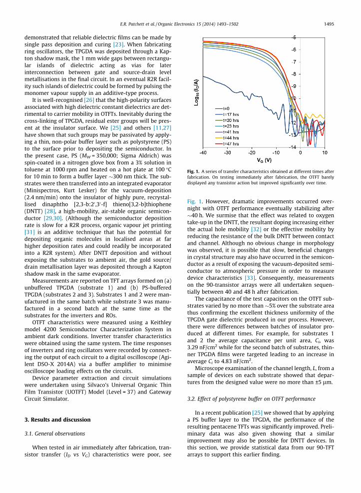
Fig. 1. A series of transfer characteristics obtained at different times afterfabrication. On testing immediately after fabrication, the OTFT barelydisplayed any transistor action but improved significantly over time.
E.R. Patchett et al. / Organic Electronics 15 (2014) 1493–1502 1495
demonstrated that reliable dielectric films can be made bysingle pass deposition and curing [23]. When fabricatingring oscillators, the TPGDA was deposited through a Kap-ton shadow mask, the 1 mm wide gaps between rectangu-lar islands of dielectric acting as vias for laterinterconnection between gate and source-drain levelmetallisations in the final circuit. In an eventual R2R facil-ity such islands of dielectric could be formed by pulsing themonomer vapour supply in an additive-type process.
It is well-recognised [26] that the high-polarity surfacesassociated with high dielectric constant dielectrics are det-rimental to carrier mobility in OTFTs. Inevitably during thecross-linking of TPGDA, residual ester groups will be pres-ent at the insulator surface. We [25] and others [11,27]have shown that such groups may be passivated by apply-ing a thin, non-polar buffer layer such as polystyrene (PS)to the surface prior to depositing the semiconductor. Inthe present case, PS (MW = 350,000; Sigma Aldrich) wasspin-coated in a nitrogen glove box from a 3% solution intoluene at 1000 rpm and heated on a hot plate at 100 �Cfor 10 min to form a buffer layer �300 nm thick. The sub-strates were then transferred into an integrated evaporator(Minispectros, Kurt Lesker) for the vacuum-deposition(2.4 nm/min) onto the insulator of highly pure, recrystal-lised dinaphtho [2,3-b:20,30-f] thieno[3,2-b]thiophene(DNTT) [28], a high-mobility, air-stable organic semicon-ductor [29,30]. (Although the semiconductor depositionrate is slow for a R2R process, organic vapour jet printing[31] is an additive technique that has the potential fordepositing organic molecules in localised areas at farhigher deposition rates and could readily be incorporatedinto a R2R system). After DNTT deposition and withoutexposing the substrates to ambient air, the gold source/drain metallisation layer was deposited through a Kaptonshadow mask in the same evaporator.
Measurements are reported on TFT arrays formed on (a)unbuffered TPGDA (substrate 1) and (b) PS-bufferedTPGDA (substrates 2 and 3). Substrates 1 and 2 were man-ufactured in the same batch while substrate 3 was manu-factured in a second batch at the same time as thesubstrates for the inverters and ROs.
OTFT characteristics were measured using a Keithleymodel 4200 Semiconductor Characterization System inambient dark conditions. Inverter transfer characteristicswere obtained using the same system. The time responsesof inverters and ring oscillators were recorded by connect-ing the output of each circuit to a digital oscilloscope (Agi-lent DSO-X 2014A) via a buffer amplifier to minimiseoscilloscope loading effects on the circuits.
Device parameter extraction and circuit simulationswere undertaken using Silvaco’s Universal Organic ThinFilm Transistor (UOTFT) Model (Level = 37) and GatewayCircuit Simulator.
3. Results and discussion
3.1. General observations
When tested in air immediately after fabrication, tran-sistor transfer (ID vs VG) characteristics were poor, see
Fig. 1. However, dramatic improvements occurred over-night with OTFT performance eventually stabilizing after�40 h. We surmise that the effect was related to oxygentake-up in the DNTT, the resultant doping increasing eitherthe actual hole mobility [32] or the effective mobility byreducing the resistance of the bulk DNTT between contactand channel. Although no obvious change in morphologywas observed, it is possible that slow, beneficial changesin crystal structure may also have occurred in the semicon-ductor as a result of exposing the vacuum-deposited semi-conductor to atmospheric pressure in order to measuredevice characteristics [33]. Consequently, measurementson the 90-transistor arrays were all undertaken sequen-tially between 40 and 48 h after fabrication.
The capacitance of the test capacitors on the OTFT sub-strates varied by no more than �5% over the substrate areathus confirming the excellent thickness uniformity of theTPGDA gate dielectric produced in our process. However,there were differences between batches of insulator pro-duced at different times. For example, for substrates 1and 2 the average capacitance per unit area, Ci, was3.29 nF/cm2 while for the second batch of substrates, thin-ner TPGDA films were targeted leading to an increase inaverage Ci to 4.83 nF/cm2.
Microscope examination of the channel length, L, from asample of devices on each substrate showed that depar-tures from the designed value were no more than ±5 lm.
3.2. Effect of polystyrene buffer on OTFT performance
In a recent publication [25] we showed that by applyinga PS buffer layer to the TPGDA, the performance of theresulting pentacene TFTs was significantly improved. Preli-minary data was also given showing that a similarimprovement may also be possible for DNTT devices. Inthis section, we provide statistical data from our 90-TFTarrays to support this earlier finding.

Fig. 3. Transfer characteristics in the linear and saturation regimes forone of the devices from Fig. 2(b) formed on PS-TPGDA. Also shown are thegate leakage current, IG, (dotted curves) and the gate voltage dependenceof mobility in both regimes (inset).
1496 E.R. Patchett et al. / Organic Electronics 15 (2014) 1493–1502
In Fig. 2 are the linear and saturation transfer character-istics of blocks of 9 adjacent transistors with common gate(see inset of Fig. 2(a)) formed on (a) TPGDA (1 devicefailed) and (b) on PS-buffered TPGDA. Without buffering,strong hysteresis is observed when sweeping VG from10 V to �60 V and back again. This, and the lack of overlapbetween linear and saturation characteristics in the lowercurrent regimes, are symptomatic of an unstable thresholdvoltage. Nevertheless, turn-on voltages are in the range±10 V and even though off-currents are relatively high,especially in saturation, on–off ratios are �105.
In contrast, the off-currents of the PS-TPGDA devices inthe linear regime are below the noise floor of our measure-ment system (�1 pA) and increase to only �10 pA in satu-ration, leading to on–off ratios in excess of 106. Some ofthese devices displayed a shallower subthreshold slope atlow currents, probably arising from a higher interface trapdensity [34]. However, no hysteresis was observedbetween the forward and reverse voltage sweeps, as evi-denced by the transfer characteristics in Fig. 3 of one ofthe devices from Fig. 2(b). In almost all PS-buffered devicesthe gate leakage current, IG, was independent of source–drain voltage, VD, but greater than the off-current, suggest-ing that gate–source leakage dominated gate current.
Device current, ID, in the linear regime is given by
ID ¼WL
llinCi VG � VTð ÞVD ð1Þ
and in saturation by
ID ¼W2L
lsatCi VG � VTð Þ2 ð2Þ
where VT is the threshold voltage. The mobilities in the lin-ear (llin) and saturation (lsat) regimes were extracted fromthe local slopes of the transfer plots using, respectively, theequations [35]
llin ¼@ID
@VG� LWCiVD
ð3Þ
Fig. 2. Transfer characteristics in the linear and saturation regimes for blocks ofgate insulators. The inset in (a) shows a schematic plan view of one of the 10illustrates the current flow lines between source and drain near the tip of one e
and
lsat ¼@ffiffiffiffiffiIDp
@VG
� �2
� 2LWCi
ð4Þ
It should be noted, though, that these equations areonly valid when the mobility is weakly dependent on gatevoltage and can lead to an over-estimate when mobilityincreases strongly with VG while under-estimating whenmobility decreases with VG [36].
With this caveat, extracted mobilities from the transfercharacteristics in Fig. 3 are plotted as a function of VG inthe figure inset. Both llin and lsat begin to increase rapidlyat about �7 V following similar paths. As VG becomes morenegative, llin rises more rapidly, eventually reaching a max-imum of 1.29 cm2/V s before decreasing to 1.24 cm2/V s
9 � DNTT TFTs fabricated on (a) TPGDA (1 device failed) and (b) PS-TPGDAblocks of 9 TFTs with common gate on each substrate while that in (b)lectrode.
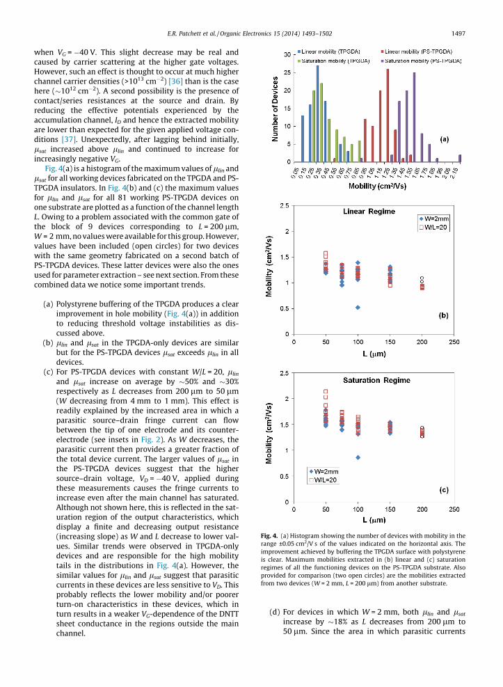
Fig. 4. (a) Histogram showing the number of devices with mobility in therange ±0.05 cm2/V s of the values indicated on the horizontal axis. Theimprovement achieved by buffering the TPGDA surface with polystyreneis clear. Maximum mobilities extracted in (b) linear and (c) saturationregimes of all the functioning devices on the PS-TPGDA substrate. Alsoprovided for comparison (two open circles) are the mobilities extractedfrom two devices (W = 2 mm, L = 200 lm) from another substrate.
E.R. Patchett et al. / Organic Electronics 15 (2014) 1493–1502 1497
when VG = �40 V. This slight decrease may be real andcaused by carrier scattering at the higher gate voltages.However, such an effect is thought to occur at much higherchannel carrier densities (>1013 cm�2) [36] than is the casehere (�1012 cm�2). A second possibility is the presence ofcontact/series resistances at the source and drain. Byreducing the effective potentials experienced by theaccumulation channel, ID and hence the extracted mobilityare lower than expected for the given applied voltage con-ditions [37]. Unexpectedly, after lagging behind initially,lsat increased above llin and continued to increase forincreasingly negative VG.
Fig. 4(a) is a histogram of the maximum values of llin andlsat for all working devices fabricated on the TPGDA and PS-TPGDA insulators. In Fig. 4(b) and (c) the maximum valuesfor llin and lsat for all 81 working PS-TPGDA devices onone substrate are plotted as a function of the channel lengthL. Owing to a problem associated with the common gate ofthe block of 9 devices corresponding to L = 200 lm,W = 2 mm, no values were available for this group. However,values have been included (open circles) for two deviceswith the same geometry fabricated on a second batch ofPS-TPGDA devices. These latter devices were also the onesused for parameter extraction – see next section. From thesecombined data we notice some important trends.
(a) Polystyrene buffering of the TPGDA produces a clearimprovement in hole mobility (Fig. 4(a)) in additionto reducing threshold voltage instabilities as dis-cussed above.
(b) llin and lsat in the TPGDA-only devices are similarbut for the PS-TPGDA devices lsat exceeds llin in alldevices.
(c) For PS-TPGDA devices with constant W/L = 20, llin
and lsat increase on average by �50% and �30%respectively as L decreases from 200 lm to 50 lm(W decreasing from 4 mm to 1 mm). This effect isreadily explained by the increased area in which aparasitic source–drain fringe current can flowbetween the tip of one electrode and its counter-electrode (see insets in Fig. 2). As W decreases, theparasitic current then provides a greater fraction ofthe total device current. The larger values of lsat inthe PS-TPGDA devices suggest that the highersource–drain voltage, VD = �40 V, applied duringthese measurements causes the fringe currents toincrease even after the main channel has saturated.Although not shown here, this is reflected in the sat-uration region of the output characteristics, whichdisplay a finite and decreasing output resistance(increasing slope) as W and L decrease to lower val-ues. Similar trends were observed in TPGDA-onlydevices and are responsible for the high mobilitytails in the distributions in Fig. 4(a). However, thesimilar values for llin and lsat suggest that parasiticcurrents in these devices are less sensitive to VD. Thisprobably reflects the lower mobility and/or poorerturn-on characteristics in these devices, which inturn results in a weaker VG-dependence of the DNTTsheet conductance in the regions outside the mainchannel.
(d) For devices in which W = 2 mm, both llin and lsat
increase by �18% as L decreases from 200 lm to50 lm. Since the area in which parasitic currents
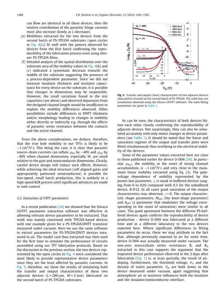
Fig. 5. Transfer and output (inset) characteristics of two adjacent devices(data points) formed on the second batch of PS-TPGDA. The solid lines aresimulations obtained using the Silvaco UOTFT software. The main fittingparameters are given in Table 1.
1498 E.R. Patchett et al. / Organic Electronics 15 (2014) 1493–1502
can flow are identical in all these devices, then therelative contribution of the parasitic fringe currentsmust also increase slowly as L decreases.
(e) Mobilities extracted for the two devices from thesecond batch of PS-TPGDA substrates (open circlesin Fig. 4(c)) fit well with the pattern observed fordevices from the first batch confirming the repro-ducibility of the fabrication process even using thin-ner PS-TPGDA films.
(f) Detailed analysis of the spatial distribution over thesubstrate area of the mobility values in Fig. 4(b) and(c) indicated a systematic decrease towards themiddle of the substrate suggesting the presence ofa process-dependent parameter. Since we did notmeasure insulator thickness and insulator capaci-tance for every device on the substrate, it is possiblethat changes in dimensions may be responsible.However, the small variations found in the testcapacitors (see above) and observed departures fromthe designed channel length would be insufficient toexplain the mobility differences observed. Otherpossibilities include differences in DNTT thicknessand/or morphology leading to changes in mobilityeither directly or indirectly e.g. through the effectsof parasitic series resistance between the contactsand the active channel.
From the above considerations, we deduce, therefore,that the true hole mobility in our TFTs is likely to be�1 cm2/V s. This being the case, it is clear that parasiticsource–drain currents can inflate llin by �40% and lsat by�80% when channel dimensions, especially W, are smallrelative to the gate and semiconductor dimensions. Clearly,careful device design will reduce such effects. However,while achieving the ideal structure (self aligned gates andappropriately patterned semiconductor) is possible forlow-speed, small batch production, this is unlikely in ahigh speed R2R process until significant advances are madein web control.
3.3. Extraction of OTFT parameters
In a recent publication [24] we showed that the SilvacoUOTFT parameter extraction software was effective inallowing relevant device parameters to be extracted. Thatwork was mainly concerned with TPGDA-based deviceswith one example given for a PS-TPGDA/DNTT transistormeasured under vacuum. Here we use the same softwareto extract parameters for PS-TPGDA/DNTT devices mea-sured in air. The model card thus extracted was then usedfor the first time to simulate the performance of circuitsassembled using our TFT fabrication protocols. Based onthe discussion in the previous section, the two devices rep-resented by the open circles in Fig. 4 were considered themost likely to provide representative device parameterssince they are the least affected by parasitic currents. InFig. 5, therefore, we show the results of simulating boththe transfer and output characteristics of these twoadjacent devices (L = 200 lm, W = 2 mm) fabricated onthe second batch of PS-TPGDA substrates.
As can be seen, the characteristics of both devices fol-low each other closely confirming the reproducibility ofadjacent devices. Not surprisingly, they can also be simu-lated accurately with only minor changes in device param-eters (see Table 1). It should be noted that the linear andsaturation regimes of the output and transfer plots werefitted simultaneously thus testifying to the electrical stabil-ity of the devices.
Some of the parameter values extracted here are closeto those published earlier for device O-D04 [24]. In partic-ular lACC, the mobility at the onset of strong channelaccumulation, is �1 cm2/V s and very close to the maxi-mum linear mobility extracted using Eq. (3). The gate-voltage dependence of mobility represented by thepower-law parameter, c, is weak in buffered devices rang-ing from 0 to 0.03 compared with 0.3 for the unbuffereddevice, B-D12. In all cases good saturation of the outputcharacteristics was observed, k = 0. The output character-istic shape parameters, MSAT (the knee-shape parameter)and ASAT (a parameter that modulates the voltage corre-sponding to the onset of saturation) were similar in allcases. This good agreement between the different PS-buf-fered devices again confirms the reproducibility of deviceproduction – device O-D04 was fabricated at a differenttime and in a different laboratory to the two devicesreported here. Where significant differences in fittingparameters do occur, these we may attribute to the factthat, although previously exposed to air for some time,device O-D04 was actually measured under vacuum. Thenon-zero source/drain series resistances RS and RD
extracted in this case supports the argument that theimproved device performance observed in the 2 days afterfabrication (Fig. 1) is, at least partially, the result of air-doping. Furthermore, the threshold voltage, VT, and thedensity of states parameter, V0, are both lower in thedevice measured under vacuum, again suggesting thatatmospheric air or moisture influences both the insulatorand the insulator/semiconductor interface.

Table 1Fitting parameters for DNTT devices with different gate dielectrics. The parameters are described in the text except for r0 the minimum bulk conductance. Itwas assumed in all the simulations that, the characteristic voltage of the effective mobility, VACC = 1 and the leakage saturation current, IOL = 3 fA. Theparameters for devices B-D12 and O-D04 were reported previously [24].
Parameter B-D12 O-D04 This work
Device 1 (3E03) Device 2 (3E04)
Insulator TPGDA TPGDA/polystyrene TPGDA/polystyrene TPGDA/polystyreneAmbient Air Vacuum Air AirW (lm) 3000 2400 2000 2000L (lm) 150 200 200 200Ci (F/cm2) 5.84 � 10�9 1.28 � 10�8 4.83 � 10�9 4.83 � 10�9
VT (V) �4.78 �1.31 �17.86 �18.4VO (V) 3.12 0.307 0.948 0.893VACC 1 1 1 1lACC (cm2/V s) 0.0391 1.05 1.07 1.08c 0.362 0 0.031 0k 0 0 0 0MSAT 3.41 2.58 3.90 3.57ASAT 1.421 1.41 1.19 1.16r0 (S) 1 � 10-20 1 � 10�13 8.66 � 10�15 2.44 � 10�14
RS (X) 0 7.39 � 104 0 0RD (X) 0 8.66 � 104 0 0
E.R. Patchett et al. / Organic Electronics 15 (2014) 1493–1502 1499
3.4. PS-TPGDA/DNTT inverter
Using PS-buffered TPGDA as the gate insulator and asimilar transistor design to that in Fig. 2, batches of 27 uni-polar, saturated-load inverters (inset Fig. 6) were fabri-cated on each of 10 substrates (2nd batch of PS-TPGDA)with a 100% yield being achieved. The W/L ratios for thedriver and load transistors were (2500 lm)/(50 lm) and(625 lm)/(100 lm) respectively. The inset in Fig. 6 demon-strates the inverter response to a slowly varying squarewave and confirms stable device operation. The main fig-ure shows the experimentally obtained voltage transfercharacteristics for the device (points) for different supplyvoltages (VDD). For comparison we also give the simulatedresponse (lines) based on the model card in Table 1 for
Fig. 6. Experimentally-measured inverter voltage transfer characteristics(points) for different supply voltages, VDD. Also shown (lines) aresimulations based on the model card for transistor 3E03 (see Table 1).The insets show the saturated load inverter circuit and the inverterresponse to a square wave input signal with VDD = �40 V.
Device 1 but with the appropriate values for W and Lsubstituted for the driver and load transistors.
The simulated plots obtained using Silvaco’s GatewaySPICE-modeller, provide a reasonable match to the experi-mental results over much of the operational range. How-ever, they clearly underestimate the ‘pull-up’ ability ofthe load transistor. This is not surprising given the effectof device geometry on the saturation mobility in Fig. 4(c).While the relative magnitude of the parasitic source–draincurrent effect will be small in the driver transistor(W = 2.5 mm) compared to Device 1 (W = 2 mm), it willbe much greater in the saturated load transistor(W = 0.625 mm). To achieve improved simulations, there-fore, it would be necessary to include in the TFT model adescription of the additional VD-dependent parasiticsource–drain current depicted in Fig. 2(b). Alternatively,the simulation could be validated in additional experi-ments in which the semiconductor is appropriately pat-terned as discussed earlier.
3.5. PS-TPGDA/DNTT ring oscillators
Using the same high-yield fabrication protocols estab-lished for the TFTs and inverters, both 5- and 7-stage ringoscillators (ROs) were fabricated, again on the 2nd batchof PS-TPGDA substrates. As shown in the inset of Fig. 8,the ROs were based on inverters composed of a driver tran-sistor, W/L = (4000 lm)/(50 lm), and a saturated transistorload, W/L = (400 lm)/(50 lm). Measurements on the 7-stage device were commenced some 21 h after the finalfabrication step i.e. during the period when transistor per-formance was close to, but not in, the stable range follow-ing the initial increase (Fig. 1). The 5-stage device was keptin a sealed, translucent plastic box under laboratory condi-tions for 1 month prior to measurements. For both cases,the devices began to generate an output signal >100 Hzeven with VDD as low as �15 V (Fig. 7). On increasingVDD, device frequencies increased non-linearly. WithVDD = �90 V the 5-stage RO achieved an output frequency
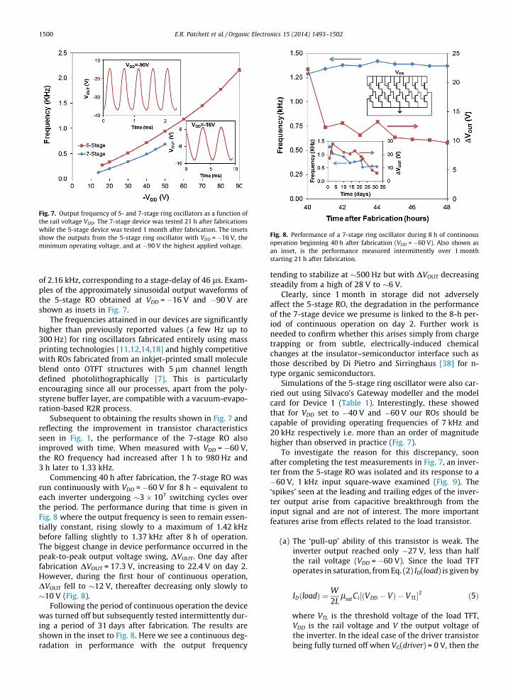
Fig. 7. Output frequency of 5- and 7-stage ring oscillators as a function ofthe rail voltage VDD. The 7-stage device was tested 21 h after fabricationswhile the 5-stage device was tested 1 month after fabrication. The insetsshow the outputs from the 5-stage ring oscillator with VDD = �16 V, theminimum operating voltage, and at �90 V the highest applied voltage.
Fig. 8. Performance of a 7-stage ring oscillator during 8 h of continuousoperation beginning 40 h after fabrication (VDD = �60 V). Also shown asan inset, is the performance measured intermittently over 1 monthstarting 21 h after fabrication.
1500 E.R. Patchett et al. / Organic Electronics 15 (2014) 1493–1502
of 2.16 kHz, corresponding to a stage-delay of 46 ls. Exam-ples of the approximately sinusoidal output waveforms ofthe 5-stage RO obtained at VDD = �16 V and �90 V areshown as insets in Fig. 7.
The frequencies attained in our devices are significantlyhigher than previously reported values (a few Hz up to300 Hz) for ring oscillators fabricated entirely using massprinting technologies [11,12,14,18] and highly competitivewith ROs fabricated from an inkjet-printed small moleculeblend onto OTFT structures with 5 lm channel lengthdefined photolithographically [7]. This is particularlyencouraging since all our processes, apart from the poly-styrene buffer layer, are compatible with a vacuum-evapo-ration-based R2R process.
Subsequent to obtaining the results shown in Fig. 7 andreflecting the improvement in transistor characteristicsseen in Fig. 1, the performance of the 7-stage RO alsoimproved with time. When measured with VDD = �60 V,the RO frequency had increased after 1 h to 980 Hz and3 h later to 1.33 kHz.
Commencing 40 h after fabrication, the 7-stage RO wasrun continuously with VDD = �60 V for 8 h – equivalent toeach inverter undergoing �3 � 107 switching cycles overthe period. The performance during that time is given inFig. 8 where the output frequency is seen to remain essen-tially constant, rising slowly to a maximum of 1.42 kHzbefore falling slightly to 1.37 kHz after 8 h of operation.The biggest change in device performance occurred in thepeak-to-peak output voltage swing, DVOUT. One day afterfabrication DVOUT = 17.3 V, increasing to 22.4 V on day 2.However, during the first hour of continuous operation,DVOUT fell to �12 V, thereafter decreasing only slowly to�10 V (Fig. 8).
Following the period of continuous operation the devicewas turned off but subsequently tested intermittently dur-ing a period of 31 days after fabrication. The results areshown in the inset to Fig. 8. Here we see a continuous deg-radation in performance with the output frequency
tending to stabilize at �500 Hz but with DVOUT decreasingsteadily from a high of 28 V to �6 V.
Clearly, since 1 month in storage did not adverselyaffect the 5-stage RO, the degradation in the performanceof the 7-stage device we presume is linked to the 8-h per-iod of continuous operation on day 2. Further work isneeded to confirm whether this arises simply from chargetrapping or from subtle, electrically-induced chemicalchanges at the insulator–semiconductor interface such asthose described by Di Pietro and Sirringhaus [38] for n-type organic semiconductors.
Simulations of the 5-stage ring oscillator were also car-ried out using Silvaco’s Gateway modeller and the modelcard for Device 1 (Table 1). Interestingly, these showedthat for VDD set to �40 V and �60 V our ROs should becapable of providing operating frequencies of 7 kHz and20 kHz respectively i.e. more than an order of magnitudehigher than observed in practice (Fig. 7).
To investigate the reason for this discrepancy, soonafter completing the test measurements in Fig. 7, an inver-ter from the 5-stage RO was isolated and its response to a�60 V, 1 kHz input square-wave examined (Fig. 9). The‘spikes’ seen at the leading and trailing edges of the inver-ter output arise from capacitive breakthrough from theinput signal and are not of interest. The more importantfeatures arise from effects related to the load transistor.
(a) The ‘pull-up’ ability of this transistor is weak. Theinverter output reached only �27 V, less than halfthe rail voltage (VDD = �60 V). Since the load TFToperates in saturation, from Eq. (2) ID(load) is given by
ID loadð Þ ¼W2L
lsatCi VDD � Vð Þ � VTL½ �2 ð5Þ
where VTL is the threshold voltage of the load TFT,
VDD is the rail voltage and V the output voltage ofthe inverter. In the ideal case of the driver transistorbeing fully turned off when VG(driver) = 0 V, then the
Fig. 9. Response of an inverter stage from the 5-stage ring oscillator(VDD = �60 V). Fig. 10. Effect of parasitic capacitances on the 5-stage ring oscillator
frequency deduced from simulations with VDD = �60 V. The inset showsthe ring oscillator circuit including parasitic gate–source, Cgs, and gate–drain, Cgd, capacitances added to the driver (D) and load (L) OTFTs. In thesimulation it was assumed that CgdD = CgsD = 5CgsL.
E.R. Patchett et al. / Organic Electronics 15 (2014) 1493–1502 1501
inverter output of �27 V would correspond to thecondition (VDD � V � VTL) = 0, suggesting a shift inVTL to �33 V as a result of bias stress while acquiringthe results in Fig. 7. This is likely to be an over-esti-mate, however, owing to the non-zero off-current ofthe driver TFT.
(b) When measuring the inverter response in Fig. 9, thebuffer amplifier and coaxial cable presented a loadcapacitance of �48 pF at the inverter output. Owingto the lower on-conductance of the load transistor,the time to charge this capacitance via the loadTFT, �0.3 ms, is longer than for discharging throughthe driver TFT,�0.1 ms. In the case of the RO, the rel-evant capacitance is the channel capacitance, WLCi �10 pF, of the driver TFT of the following stage, sug-gesting that the RO should be capable of operatingwell above 10 kHz. However, such considerationsneglect the effect of parasitic capacitances, espe-cially gate–source, Cgs, and gate–drain, Cgd, overlapcapacitances.
In Fig. 10 we show the results of simulations in whichthe effect of these capacitances on the 5-stage RO fre-quency was investigated. In the simulations it wasassumed that VDD = �60 V and that, based on the transistordesigns, the gate overlap in the driver transistors was sym-metrical so that CgsD = CgdD and that for the load TFTCgsL = 0.2CgdD.
It is obvious that overlap capacitances seriously impairRO operation, with the simulated output frequencydecreasing from 20 kHz with no parasitic capacitance toless than 1 kHz when CgdD > 22 pF. When measureddirectly, CgdD = 35 pF and CgsD = 50 pF owing to slight regis-tration errors during fabrication. According to Fig. 4(c), theaspect ratio of the load transistors in the ring oscillator, W/L = (400 lm)/(50 lm), is such that parasitic currents wouldmake an even greater contribution to the overestimate ofsaturation mobility than was observed for the devices inwhich W/L = (1000 lm)/(50 lm). The true conductance ofthe load TFTs would have been much greater, therefore,than expected from the designed width, W. In a firstapproximation to account for this effect, the conductance
of the load transistors was doubled by increasing the effec-tive W to 800 lm. With these more realistic valuesincluded in the model, the simulated RO oscillated at1 kHz and close to the measured frequency of 1.12 kHz.Interestingly, had the misalignment error led to a reversalin the values of CgdD and CgsD, the simulated RO frequencywould have decreased below 500 Hz i.e. gate–drain overlapcapacitance of the driver TFT, CgdD, has a greater degradingeffect than the gate-source capacitance, CgsD. Not unex-pectedly, therefore, registration and gate overlap capaci-tances will be important issues to manage in a high-speed R2R process.
4. Conclusions
We have demonstrated that bottom-gate DNTT transis-tors with mobility �1 cm2/V s can be fabricated routinelyand reproducibly with yields P90%. Apart from the poly-styrene buffer layer applied to the TPGDA all fabricationsteps were based on vacuum-evaporation and compatiblewith a R2R process. Interestingly, optimum device perfor-mance was achieved some 40 h after removing the devicesfrom the evaporator following the final metallisation step.By characterising 90-transistor arrays on each substrate wehave obtained statistical information on the likely spreadin mobility values as well as on the effect of parasiticsource–drain currents which, in smaller devices W 6 1 mmresults in the mobility in saturation being overestimatedby more than 50%. By choosing TFTs in which parasitic cur-rents were considered negligible, a model card of relevantparameters was derived by simultaneously fitting transferand output characteristics using Silvaco’s UOTFT model.The model card was then applied successfully to simulateinverter operation using Silvaco’s Gateway simulator.
Unipolar inverters based on a saturated-transistor loadand coupled to a buffer amplifier presenting a load capac-itance of 48 pF and with VDD = �60 V, were shown to becapable of undergoing a full switching cycle in �0.4 ms
1502 E.R. Patchett et al. / Organic Electronics 15 (2014) 1493–1502
corresponding to a switching frequency of 2.5 kHz. Whencoupled in series with other inverters to form 5- and 7-stage ring oscillators, significantly shorter switching timescorresponding to operational frequencies >10 kHz wereanticipated owing to the lower load capacitance, �10 pF,presented by the accumulation channel of the driver tran-sistor of the following stage. In the event, the output fre-quencies of a 5-stage RO ranged from 270 Hz atVDD = �16 V to 2.16 kHz when VDD = �90 V. Simulationsshowed that the degradation in performance was causedby gate–source and gate–drain overlap capacitances, withthe latter having the greater effect because of the smallersize of the load transistor. When these are taken intoaccount, together with an allowance for the parasitic-cur-rent-enhanced performance of the load TFTs, a reasonablematch between experimental and simulated frequencieswas obtained.
We have also shown that a ring oscillator based onDNTT/PS-buffered TPGDA TFTs can operate continuouslyfor 8 h at VDD = �60 V with relatively little change in out-put frequency albeit that a reduction in amplitude occurs.When tested intermittently over the following month, theRO continued to operate but displayed reductions in boththe frequency and amplitude of the output signal. A non-encapsulated RO stored without bias under atmosphericconditions for a month performs as well as a pristinedevice. We conclude from these observations that continu-ous operation for long periods initially, can lead toenhanced atmospheric degradation during later storage.
In conclusion, we have demonstrated that functional,environmentally stable organic electronic circuits can befabricated reproducibly with high yield using low-cost,vacuum-evaporation-based processes that are common inthe packaging industry. However, improving circuit perfor-mance by minimising gate overlap capacitances must be akey target for future R2R processes.
Acknowledgements
This work was supported by funding from theEngineering and Physical Sciences Research Council (UK)via a Flagship Grant (FS/01/01/10) from the Innovativeelectronic-Manufacturing Research Centre, Loughborough.The authors are grateful to Dr. A. Nejim of Silvaco UK Ltd.for access to and support for the UOTFT and Gatewaysimulation software.
References
[1] S.K. Park, J.E. Anthony, T.N. Jackson, IEEE Electron. Dev. Lett. 28(2007) 877.
[2] J. Li, Y. Zhao, H.S. Tan, Y. Guo, C.-A. Di, G. Yu, Y. Liu, M. Lin, S.H. Lim, Y.Zhou, H. Su, B.S. Ong, Sci. Rep. 2 (2012) 754.
[3] M.-B. Madoc, D. Crouch, G.R. Llorente, T.J. Whittle, M. Geoghegan,S.G. Yeates, J. Mater. Chem. 18 (2008) 3230.
[4] J. Smith, W. Zhang, R. Sougrat, K. Zhao, R. Li, D. Cha, A. Amassian, M.Heeney, I. McCulloch, T.D. Anthopoulos, Adv. Mater. 24 (2012) 2441.
[5] H. Sirringhaus, T. Kawase, R.H. Friend, T. Shimoda, M. Inbasekaran,W. Wu, E.P. Woo, Science 290 (2000) 2123.
[6] T. Kawase, H. Sirringhaus, R.H. Friend, T. Shimoda, Adv. Mater. 13(2001) 1601.
[7] B.K.C. Kjellander, W.T.T. Smaal, K. Myny, J. Genoe, W. Dehaene, P.Heremans, G.H. Gelinck, Org. Electron. 14 (2013) 768.
[8] A. de la, F. Vornbrock, D. Sung, H. Kang, R. Kitsombooloha, V.Subramanian, Org. Electron. 11 (2010) 2037.
[9] D. Tobjörk, N.J. Kaihovirta, T. Mälelä, F.S. Pettersson, R. Österbacka,Org. Electron. 9 (2008) 931.
[10] S. Chung, S.O. Kim, S.-K. Kwon, C. Lee, Y. Hong, IEEE Electron. Dev.Lett. 32 (2011) 1134.
[11] A.C. Huebler, F. Doetz, H. Kempa, H.E. Katz, M. Bartzsch, N. Brandt, I.Hennig, U. Fuegmann, S. Vaidyanathan, J. Granstrom, S. Liu, A.Sydorenko, T. Zillger, G. Schmidt, K. Preissler, E. Reichmanis, P.Eckerle, F. Richter, T. Fischer, U. Hahn, Org. Electron. 8 (2007) 480.
[12] M. Hambsch, K. Reuter, M. Stanel, G. Schmidt, H. Kempa, U.Flügmann, U. Hahn, A.C. Hübler, Mater. Sci. Eng. B170 (2010) 93.
[13] M.M. Voigt, A. Guite, D.-Y. Chung, R.W.A. Kahn, A.J. Campbell, D.D.C.Bradley, F. Meng, J.H.G. Steinke, S. Tierney, I. McCulloch, H. Penxteen,L. Lutsen, O. Douheret, J. Manca, U. Brokmann, K. Sönnischen, D.Hülsenberg, W. Bock, C. Barron, N.B. Blankaert, S. Springer, J. Grupp,A. Mosley, Adv. Funct. Mater. 20 (2010) 239.
[14] J.-M. Verilac, M. Benwadih, A.-L. Seiler, S. Jacob, C. Bory, J. Bablet, M.Heitzman, J. Tallal, L. Barbut, P. Frère, G. Sicard, R. Gwoziecki, I.Chartier, R. Coppard, C. Serbutoviez, Org. Electron. 11 (2010) 456.
[15] J. Noh, M. Jung, K. Jung, J. Lee, J. Kim, S. Lim, D. Kim, Y. Choi, Y. Kim, V.Subramanian, G. Cho, IEE Electron. Dev. Lett. 32 (2011) 638.
[16] J. Noh, S. Kim, K. Jung, J. Kim, S. Cho, G. Cho, IEEE Electron. Dev. Lett.32 (2011) 1555.
[17] J. Noh, K. Jung, J. Kim, S. Cho, G. Cho, IEEE Electron. Dev. Lett. 33(2012) 1574.
[18] A.C. Huebler, G. Schmidt, H. Kempa, K. Reuter, M. Hambsch, M.Bellmann, Org. Electron. 12 (2011) 419.
[19] N. Copeland, A. Jack, L. Harland, Proceedings of the 52nd Society ofVacuum Coaters Conference (SVC), Santa Clara, CA, (unpublished),9–14 May 2009, p. 30.
[20] C.A. Bishop, Vacuum Deposition onto Webs, Films and Foils, WilliamAndrew Publishing, Norwich, NY, 2006.
[21] J. Affinito, Thin Sol. Films 420–421 (2002) 1.[22] G. Abbas, H. Assender, M. Ibrahim, D.M. Taylor, J. Vac. Sci. Technol.
B29 (2011) 052401.[23] G. Abbas, Z. Ding, K. Mallik, H. Assender, D.M. Taylor, Electron. Dev.
Lett. 34 (2013) 268.[24] D.M. Taylor, A. Williams, E.R. Patchett, G.A. Abbas, Z. Ding, H.E.
Assender, J.J. Morrison, S.G. Yeates, IEEE J. Display Technol. 9 (2013)877.
[25] Z. Ding, G.A.W. Abbas, H.E. Assender, J.J. Morrison, V. Sanchez-Romaguera, S.G. Yeates, D.M. Taylor, Appl. Phys. Lett. 103 (2013)233301.
[26] J. Veres, S. Ogier, G. Lloyd, D. de Leeuw, Chem. Mater. 16 (2004)4543.
[27] A. Yu, Q. Qi, P. Jiang, C. Jiang, Synth. Met. 159 (2009) 1467.[28] T. Yamamoto, K. Takimiya, JACS 129 (2007) 2244.[29] U. Zschieschang, F. Ante, T. Yamamoto, K. Takimiya, H. Kuwabara, M.
Ikeda, T. Sekitani, T. Someya, K. Kern, H. Klauk, Adv. Mater. 29 (2010)982.
[30] U. Zschieschang, F. Ante, D. Kälblein, T. Yamamoto, K. Takimiya, H.Kuwabara, M. Ikeda, T. Sekitani, T. Someya, J. Blochwitz-Nimoth, H.Klauk, Org. Electron. 12 (2011) 1370.
[31] M. Shtein, P. Peumans, J.B. Benziger, S.R. Forrest, J. Appl. Phys. 96(2004) 4500.
[32] A.R. Brown, D.M. de Leeuw, E.E. Havinga, A. Pomp, Synth. Met. 68(1994) 65.
[33] K. Sakai, Phys. Rev. Lett. 110 (2013) 096603.[34] W.L. Kalb, B. Batlogg, Phys. Rev. B 81 (2010) 035327.[35] D.J. Gundlach, L. Zhou, J.A. Nichols, T.N. Jackson, J. Appl. Phys. 100
(2006) 024509.[36] M. Mottaghi, G. Horowitz, Org. Electron. 7 (2006) 528.[37] M.M. Ibrahim, A.C. Maciel, C.P. Watson, M.-B. Madec, S.G. Yeates,
D.M. Taylor, Org. Electron. 11 (2010) 1234.[38] R. Di Pietro, H. Sirringhaus, Adv. Mater. 24 (2012) 3367.