Embed Size (px)
Citation preview

A Wet Clean Solution to Reduce Unwanted eSiGe Growth Defect in FinFET Jian Li, Vincent Sih and Talapady Bhat
GLOBALFOUNDRIES, Malta, New York 12020, USA
SPCC, March 29, 2017
Junction process flow in 3D FinFET
Wet clean solution for unwanted growth defect in PFET
(p-Channel Field-effect transistor)
Defect reduction and line yield improvement on FinFET
product wafers
Conclusion
GLOBALFOUNDRIES 2
Outline
SPCC, March 29, 2017
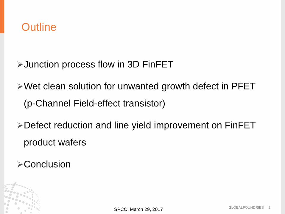
PFET Junction process flow
GLOBALFOUNDRIES 3
PFET Spacer Etch
PFET Pre eSiGe Clean
Post eSiGe Clean
PFET Defect Inspection
PFET Photo Resist Ashing
PFET eSiGe Growth
SPCC, March 29, 2017
14LPP, 14nm FinFET Technology https://www.globalfoundries.com/technology-solutions/cmos/performance/14lpp
Challenges for PFET Pre eSiGe clean
The epitaxial growth of eSiGe is very sensitive to surface condition of
substrate layer.
Any small silicon particle (even less than 10nm) could serve as synthesis
seed for eSiGe nucleation and later become a large unwanted growth
defect.
The silicon particle defect causing unwanted growth defect prior to eSiGe
growth is too tiny to be caught by the state-of-the-art SP5 CFM scanning
in current advanced manufacturing fab.
The large unwanted eSiGe defect can cause degradation of device
performance and raise the reliability concern.
GLOBALFOUNDRIES 4 SPCC, March 29, 2017
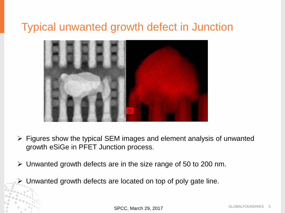
Typical unwanted growth defect in Junction
GLOBALFOUNDRIES 5
Figures show the typical SEM images and element analysis of unwanted growth eSiGe in PFET Junction process.
Unwanted growth defects are in the size range of 50 to 200 nm.
Unwanted growth defects are located on top of poly gate line.
SPCC, March 29, 2017

Wet clean solution for unwanted growth defect
6
GLOBALFOUNDRIES Confidential 7 SPCC, March 29, 2017
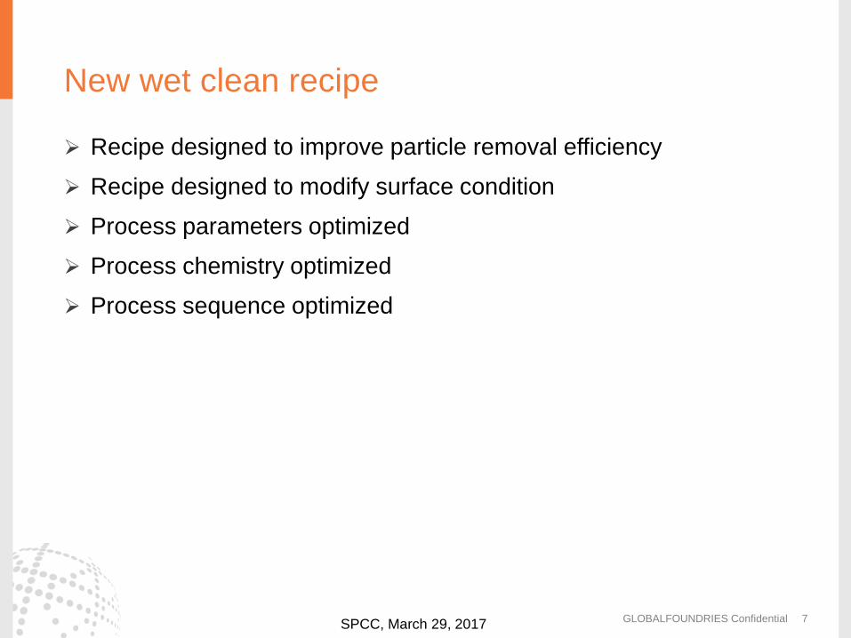
New wet clean recipe
Recipe designed to improve particle removal efficiency
Recipe designed to modify surface condition
Process parameters optimized
Process chemistry optimized
Process sequence optimized
GLOBALFOUNDRIES Confidential 8
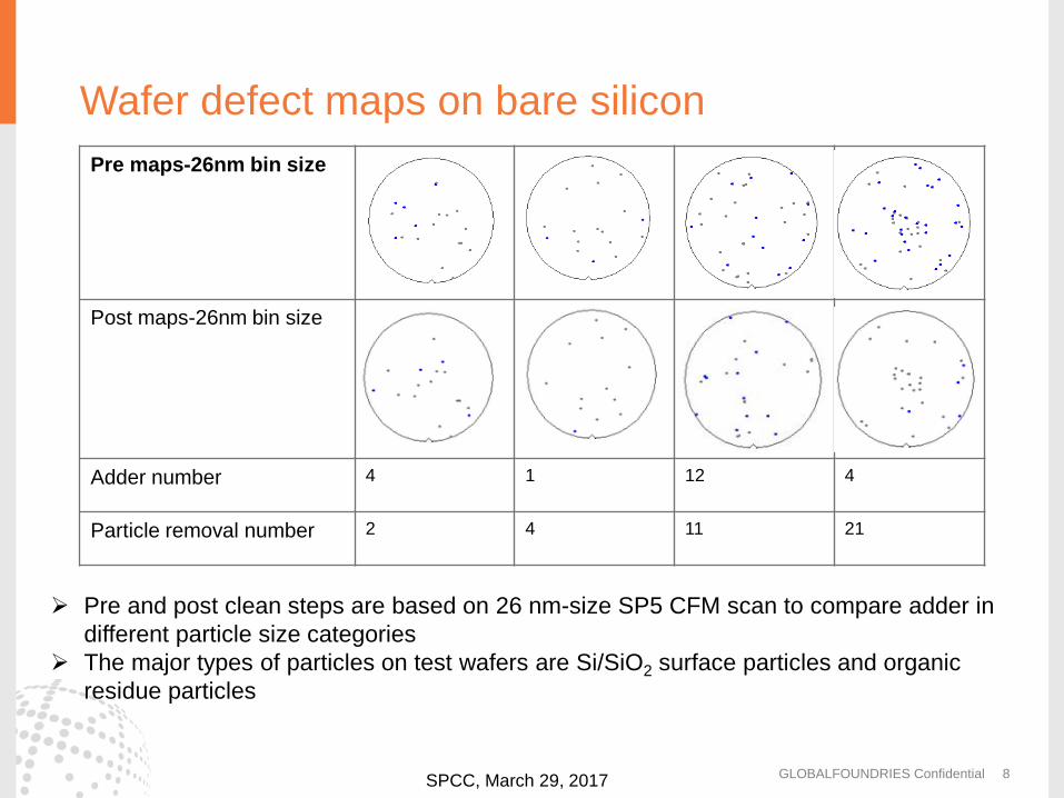
Pre maps-26nm bin size
Post maps-26nm bin size
Adder number 4 1 12 4
Particle removal number 2 4 11 21
SPCC, March 29, 2017
Wafer defect maps on bare silicon
Pre and post clean steps are based on 26 nm-size SP5 CFM scan to compare adder in different particle size categories
The major types of particles on test wafers are Si/SiO2 surface particles and organic residue particles
Defect reduction on FinFET product wafers
9
GLOBALFOUNDRIES Confidential 10
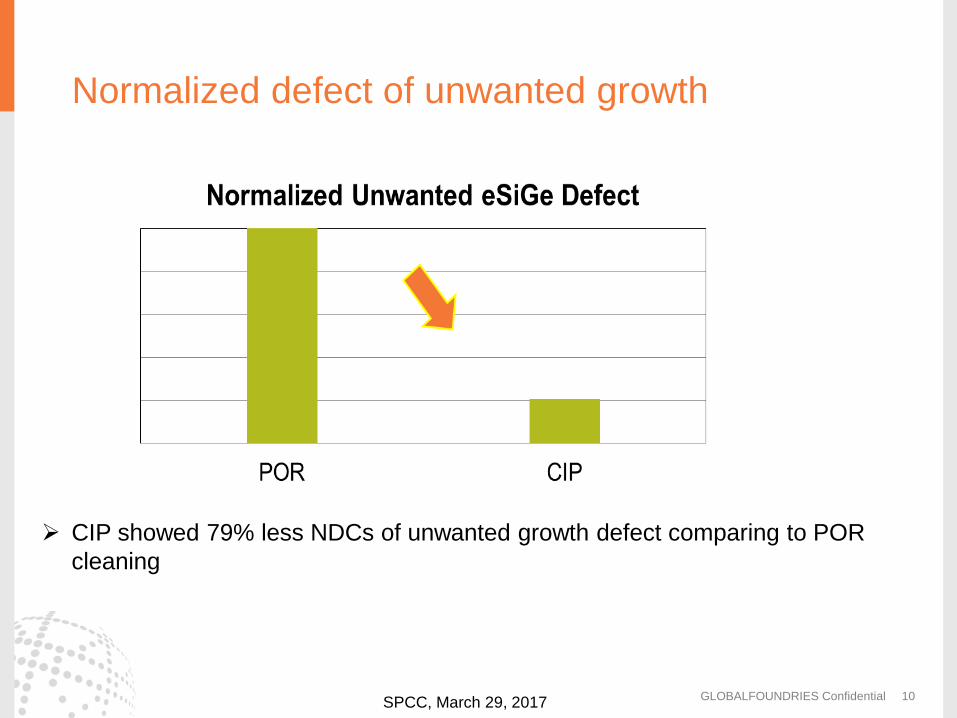
Normalized defect of unwanted growth
SPCC, March 29, 2017
CIP showed 79% less NDCs of unwanted growth defect comparing to POR cleaning
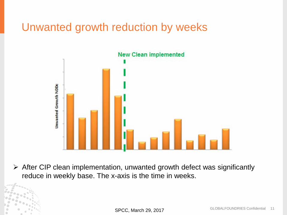
Unwanted growth reduction by weeks
GLOBALFOUNDRIES Confidential 11 SPCC, March 29, 2017
After CIP clean implementation, unwanted growth defect was significantly reduce in weekly base. The x-axis is the time in weeks.
GLOBALFOUNDRIES Confidential 12
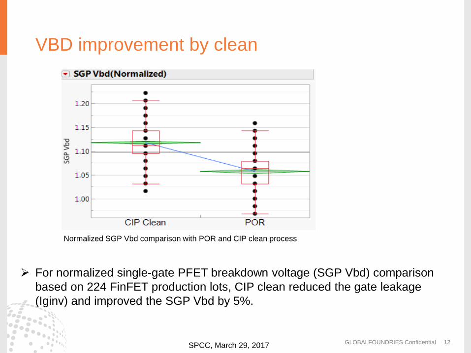
Normalized SGP Vbd comparison with POR and CIP clean process
VBD improvement by clean
SPCC, March 29, 2017
For normalized single-gate PFET breakdown voltage (SGP Vbd) comparison based on 224 FinFET production lots, CIP clean reduced the gate leakage (Iginv) and improved the SGP Vbd by 5%.
GLOBALFOUNDRIES Confidential 13
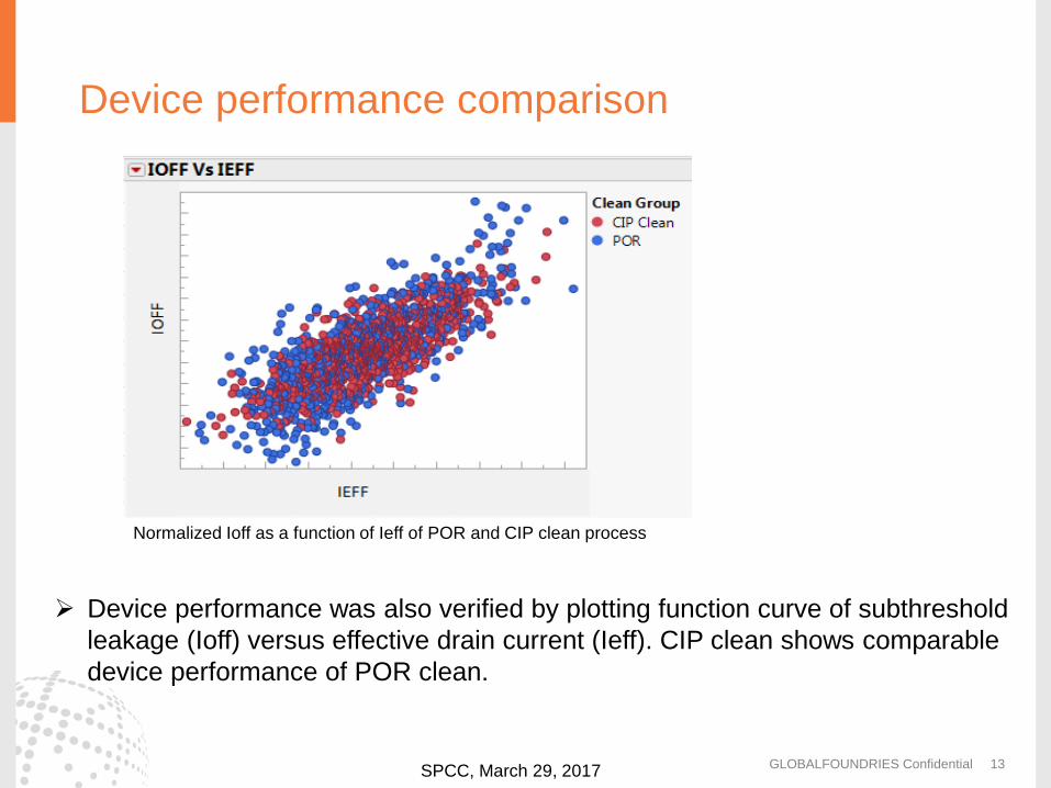
Normalized Ioff as a function of Ieff of POR and CIP clean process
Device performance comparison
SPCC, March 29, 2017
Device performance was also verified by plotting function curve of subthreshold leakage (Ioff) versus effective drain current (Ieff). CIP clean shows comparable device performance of POR clean.
Conclusion
The new cleaning can remove tiny silicon particles more efficiently and provide friendly hydrophilic surface condition for the following eSiGe growth.
Demonstrated in FinFET manufacturing for reducing ~79% unwanted eSiGe growth defect in PFET.
Observed 5% line yield improvement based on Vbd data.
The integrated wet clean solution is very promising for unwanted growth defect elimination and makes great contribution for critical rapid yield ramps in the advanced FinFET technology.
GLOBALFOUNDRIES 14 SPCC, March 29, 2017

Trademark Attribution GLOBALFOUNDRIES®, the GLOBALFOUNDRIES logo and combinations thereof, and GLOBALFOUNDRIES’ other trademarks and service marks are owned by GLOBALFOUNDRIES Inc. in the United States and/or other jurisdictions. All other brand names, product names, or trademarks belong to their respective owners and are used herein solely to identify the products and/or services offered by those trademark owners. © 2014 GLOBALFOUNDRIES Inc. All rights reserved.
Thank you Jian Li, Advance Module Engineering, GLOBALFOUNDRIES, Malta, New York 12020