Embed Size (px)
Citation preview

8122019 Alejandro Sklar Project Portfolio
httpslidepdfcomreaderfullalejandro-sklar-project-portfolio 122
$amp( $amp()($ +-($) 01)(
)+( 2(34 56(7$736 8()9($ 149 (3lt
-$amp( 8()9 34 =164 3 7ltgt6(( AB )CD D9$4 amplt( 7lt=9 amp(
77(gt )gt37( 3) 3 -36 $()1$7( amp 9$(( (9(($9 gt$7gt6()E amp( (6(7$736
))(lt )amp164 lt3F( amp( amplt( 6-3=6( $ A 3416) (3$D$14 Gamp739 amp17(79 amp( (6(7$736 9$4E
8122019 Alejandro Sklar Project Portfolio
httpslidepdfcomreaderfullalejandro-sklar-project-portfolio 222
8122019 Alejandro Sklar Project Portfolio
httpslidepdfcomreaderfullalejandro-sklar-project-portfolio 322
H($)366 $(4 amp( amplt(I) ($( (6(7$736 ))(lt
8122019 Alejandro Sklar Project Portfolio
httpslidepdfcomreaderfullalejandro-sklar-project-portfolio 422
J63$ gt3(6 K)3663
L3)9 amp( $) 366
8122019 Alejandro Sklar Project Portfolio
httpslidepdfcomreaderfullalejandro-sklar-project-portfolio 522
M Gamp739I) N1)(1lt J7(7( 34 K41)$ ONJKP
8122019 Alejandro Sklar Project Portfolio
httpslidepdfcomreaderfullalejandro-sklar-project-portfolio 622
8122019 Alejandro Sklar Project Portfolio
httpslidepdfcomreaderfullalejandro-sklar-project-portfolio 722
Circuit Noise Analysis
8122019 Alejandro Sklar Project Portfolio
httpslidepdfcomreaderfullalejandro-sklar-project-portfolio 822
$amp( Tgt-N(7amp3736 $7( N3gtgt9 8((gt J1=3-(6(9amp H63)lt7 N4() 3
$amp()($ +-($)I) S K)gt$(4 Tgt(6(7$7) 23=$3$
)+( L()(3$7amp($
Objective Investigate novel methods utilizing plasmonic nano antennae to push the
capabilities and sensitivity of atomic force microscopy utilizing current intstrumentationfor measurements of optical force of around laser modulated nano-antennae
8122019 Alejandro Sklar Project Portfolio
httpslidepdfcomreaderfullalejandro-sklar-project-portfolio 922
rXXXX American Chemical Society A dxdoiorg101021nl201780y | Nano Lett XXXX XXX 000ndash
000
LETTER
pubsacsorgNanoLett
Opto-Mechanical Force Mapping of Deep Subwavelength PlasmonicModes
John Kohoutek Dibyendu Dey Alireza Bonakdar Ryan Gelfand Alejandro Sklar Omer Gokalp Memis andHooman Mohseni
Bio-Inspired Sensors and Optoelectronics Laboratory (BISOL) EECS Northwestern University 2145 Sheridan Road EvanstonIllinois 60208 United States
bS Supporting Information
Photons have a momentum (h λ) and transfer of this mo-mentum to other objects due to elastic scattering is the
physical origin of radiation pressure and optical force This has been known to exist since deduced by Maxwell in 1871 and has
been explored in many applications1
such as solar sails for spacepropulsion2 and more recently radiation cooling34 Howevertheforce caused by unfocused light is very smallsuchthat foranapplication such as a solar sail a huge area is needed2 Previous work has shown that if the light is focused by traditional lensoptics a force large enough to measure with a probe particle ispossible and called optical trapping5 This phenomenon has been well developed by the far-1047297eld optics community68
Developmental work has been done with a probe particle held by an optical trap in 2006 to map the force induced by surfaceplasmon radiation9 Recently there has been a lot of interest toexploit the near-1047297eld region to generate an optical force tosimilarly trap particles1012 Near-1047297eld trapping was demon-strated by Righini et al in 200713 and has more recently beenused to trap even smaller particles14 Here one uses a nano-antenna to focus the light instead of a lens and the light can befocused past the diff raction limit using an integrated sourceOnce the light is focused to this point a local force in thepiconewton range may be expected as shown by simulation sofar101215 Furthermore one can then use the local trappingforces toward building a biosensor utilizing surface plasmonresonance1617 Similar structures have been used for sensing18
In fact in a micro1047298uidic setup the optical force could be used toenhance the attraction of small particles and therefore mol-ecules to the hotspot beyond the diff usion rate13141617 Alsounlike the usual trapping methods plasmonic nanostructures
are ideal for ldquochip-scalerdquo optical trapping Most importantlythis allows trapping in volumes that are many orders of magni-tude smaller than what could be achieved with far-1047297eld opticaltrapping1820 So far experimental work done to map optical
forces in the near andfar-1047297elds have used large probe particles atthe expense of high spatial resolution59 There has been littleexperimental work in measuring the optical force in the near-1047297eld with a high spatial resolution Following our recent work on measurement of Casimir force with nanometer resolution21
here we present an experimental method to accurately mapthe near-1047297eld optical force
A plasmonic nanoantenna can be used to focus light down toa spot orders of magnitude smaller than the incoming incident wavelength192022 These antennas work based on the principleof surface plasmon resonance a collective oscillation of elec-trons at the interface between metal and dielectric Because theoptical force originates from the divergence of the electromag-netic energy density23 the fact that plasmonics can be used toconcentrate the electric 1047297eld to a very small spot can leadto a very large force density On the basis of our simulationand experimental analysis1920 we have chosen a metaldielectricmetal (MDM) bowtie antenna design due to itscapability to generate higher near-1047297eld enhancement Suchstrong optical con1047297nement results in a signi1047297cant enhancementin electromagnetic 1047297eld strength and its gradient within thisregion Thus near this ldquohot spotrdquo region an optical force up to
Received May 25 2011Revised July 14 2011
ABSTRACT We present spatial mapping of optical force generated near thehot spot of a metaldielectricmetal bowtie nanoantenna at a wavelength of 1550 nm Maxwellrsquos stress tensor method has been used to simulate the opticalforce and it agrees well with the experimental data This method couldpotentially produce 1047297eld intensity and optical force mapping simultaneously
with a high spatial resolution Detailed mapping of the optical force is crucial forunderstanding and designing plasmonic-based optical trapping for emergingapplications such as chip-scale biosensing and optomechanical switching
KEYWORDS Optical force NSOM surface plasmon resonance AFMatomic force microscope biosensing
8122019 Alejandro Sklar Project Portfolio
httpslidepdfcomreaderfullalejandro-sklar-project-portfolio 1022
B dxdoiorg101021nl201780y |Nano Lett XXXX XXX 000ndash000
Nano Letters LETTER
piconewton levels per milliwatt input power can be achieved which is comparable to or higher than the forces achieved usinga far-1047297eld optical tweezer without the bulky optics necessary forthat setup5 Such compactness is crucial for building chip-scale biosensors
Our primary goal is toobserve the eff ect of the optical force onthe modulation of the amplitude of the AFM tip when it is brought in this region of optical con1047297nement Previously wehave shown that amplitude and phase require some time (sim1ms) to respond to an external force21 Thus we modulated thelaser in 50 duty cycle at low frequency (1 kHz) The operatingfrequencyof thelaser was then used as thereference signal for the
lock-in (see Figure 1 and Supporting Information FigureS2 fordetails) We then fed the output of the lock-in back to thecomputer to map to the current position of the AFM givingthe optical force intensity (see Figure 4c)
The minimum force sensitivity of our AFM system limit-ed by thermal 1047298uctuations2425 can be calculated from F min =[(4k BTkB)(ω0Q )]12 where k B is the Boltzmann constant T isroom temperature k is the spring constantof thecantilever (3 Nm) B is the bandwidth of measurement (set by lock-in ampli1047297er)used in the force measurement (78 Hz) ω0 is the resonantfrequency of the AFM tip (sim101kHz) andQ is the quality factorof the cantilever (sim160) This leads to a force sensitivity on theorder of sim40 fN in our setup Thus measuring optical force onthe order of a fraction of a piconewton is not limited by the
thermal sensitivity of our systemOur bowtie antenna is based on MDM instead of single metal
design as it has shown a considerable improvement in terms of peak intensity enhancement1920 To analyze the performanceof our MDM bowtie antenna we simulated the structure usingthree-dimensional 1047297nite-diff erence time-domain (FDTD)method The nanoantenna consists of two bowtie structuresseparated by a gap of sim50 nm The antenna was placed on thefacet of a cleaved optical 1047297 ber A plane wave with polarizationdirection along the long axis of the bowtie with wavelength of 1550 nm was used as the source for all performed FDTDsimulations During simulation a plane wave was launchedfrom the inside of the 1047297 ber core material at normal incidence to
the surface All material data used in the simulation is from ref 26 A detailed optimization of the bowtie was performedsimilar to our previously published nanoantenna designs1920
Here we used thicknesses for the two Au and SiO2 layers of 40and 30 nm respectively To 1047297nd the resonant length of each armof the bowtie we found the average intensity enhancement atthe antenna gap on the same level as the top metal surface as afunction of the varying length of each arm of the bowtie(Figure 2) To achieve better accuracy we used very 1047297ne meshsize near the antenna region PML boundary conditions wereemployed across the simulation boundary and to avoid scatter-ing eff ect on the results accuracy (primarily from the PML boundary layers) we put the boundary layers signi1047297cantly away from the antenna region (10 times the antenna length) On the basis of our simulation the optimum resonance length of 350 nm for one arm was chosen for the rest of the simulationand fabrication
We then used Maxwellrsquos stress tensor method to calculate theoptical force intensity on the AFM tip Our simulation structure
consists of a MDM box (similar to fabrication) on top of a SiO2
layer(represents the1047297 ber material) In the box the MDM bowtieantenna was positioned at the center with the correct sidewallangle generated during fabrication We modeled the AFM tipas asphere with diameter identical to the actual AFMtip (sim100 nm)The position of the AFM tip was varied and the electric 1047297eldcomponents at each position were recorded We used a single wavelength (1550 nm) plane-wave source to model the incoming beam that comes from the optical 1047297 ber The polarization of theplane wave was kept along the antenna axis We placed six planemonitors surrounding the sphere to get the electric and magnetic1047297eld components at the diff erent points of that monitor The1047297eld components are related with Maxwellrsquos stress tensor12 by
Figure 1 Experimental setup for measuring optical force The antennais fabricated on thecleaved tipof an optical1047297 ber which the AFM scans innoncontact mode The signal from the quad detector is fed to the signalin of the lock-in and the trigger out of the laser is fed to the reference inof the lock-in The laser is operated at 1 kHz at 50 duty cycle
Figure 2 Simulated average intensity enhancement versus varying armlength ( L) of the MDM bowtie antenna The free space wavelength of the incident plane wave normal to theplane is considered to be 1550 nmfor FDTD simulations Diff erent layer thicknesses of MDM were kept to
be 403040 nm (AuSiO2Au) for all performed simulations Electric1047297eld enhancement has been calculated in the middle of the gap at thelevel the of the antenna top surface using a volume monitor and
normalized with the amplitude of the incident 1047297eld The gap of theantenna was1047297 xed to be 50 nm Simulations showed maximum resonancepeak intensity at an antenna arm length of 350 nm (Inset) FDTDsimulation results showing the peak near-1047297eld intensity enhancementdistribution at a level 50 nm above the top surface of the antennas (near-1047297eld region) Simulations were performed at the resonance length of theeach arm ( L) = 350 nm
8122019 Alejandro Sklar Project Portfolio
httpslidepdfcomreaderfullalejandro-sklar-project-portfolio 1122
C dxdoiorg101021nl201780y |Nano Lett XXXX XXX 000ndash000
Nano Letters LETTER
the following formula
T ij frac14 ε0εm Ei E j
thorn μ0 μmH iH j 1
2δijethε0εmj Ej2 thorn μ0 μmjH j2THORN eth1THORN
where Ei and H i correspond to the electric and magnetic 1047297eld εmrepresents the electric permittivity and μm represents themagnetic permeability for the object on which optical force isapplied (AFM tip in our case) The electromagnetic force actingon the AFM tip has been calculated by the following formula
F ih i frac14 12
ReethZ
ST ijn jdSTHORN eth2THORN
where n j is the outward normal to the surface of the six planesmentioned before
Simulations show that the z-component of the calculatedoptical force is sim10 times larger than the in-plane (x- and y-)components and this component would also have the largesteff ect on the amplitude of the AFM tip Thus for simulated forcemapping (Figure 4d)we only considered the vertical component(z-) of the optical force exerted on the AFM tip While keepingthe vertical distance constant at 50 nm (near the average positionof the AFM tip from the antenna top surface21) we simulated thez-component of the optical force at diff erent lateral positions (x-
and y-) It is important to note that the actual force is attractivecreating a trap that can be used forbiosensingbut we have shownthe amplitude of the force The 1047297nal simulated optical forcemapping result is shown in Figure 4d
After optimizing our design we fabricated our devices on theend of a cleaved 125 μm Corning SMF-28E+ optical 1047297 ber Firstthe 1047297 ber end was coated with AuSiO2Au (403040 nm) by electron-beam evaporation The bowtie antenna was then fabri-cated on the surface of the coated 1047297 ber optic using focused ion beam (FIB) milling (Hellios FEI) Using the gallium ion beam athigh voltage (30 keV) and a very low current (92 pA) a highprecision milling was achieved The fabricated antenna on theface of the 1047297 ber optic is shown in Figure 3 Figure 3c shows an
oblique angle magni1047297ed scanning electron microscope image of the bowtie antenna
We then experimentally measured the electric 1047297eld enhance-ment using apertureless near-1047297eld scanning optical microscopy (a-NSOM see Supporting Information FigureS1 for details)1047297rst developed by Hillenbrand27 and the optical force intensity using noncontact atomic force microscopy Our custom-made
a-NSOM setup has been previously used to characterize near-1047297eld plasmonics1920 In essence it uses a lock-in ampli1047297er withthe vibrating tip frequency as the reference and the light re1047298ectedoff of the AFM tip as the signal The output of the lock-in is thenmapped to the position of the tip simultaneously giving the usera map of the topography and near-1047297eld intensity The AFM near-1047297eld map is shown in Figure 4e In this way the optical mode has been squeezed within a nanometric length scale sim150 nm that issim10 times smaller than the operating wavelength During itsoperation the sample was illuminated at sim1 mW and thepolarization of the incident beam was aligned along the longaxis of the bowtie The exact amount of coupled power to thenanoantenna was certainly lower than the laser power due todiff erent coupling losses Thus it is difficult to quantify the exact
amount of power con1047297ned in the ldquo
hot spotrdquo as done in aperture-NSOM28
Figure 4cd shows both the experiment and simulation of theoptical force map respectively Both show a central spot on theorder of 05 pN (see Supporting Information for details) andlobes at the ends of thebowtie arms where theforceis diminishedcompared to the central spot showing good agreement Thecentral spot of the experimental image is likely larger comparedto the simulation because in the simulation we considered the AFM tip as a sphere instead of using its actual pyramidalstructure The optical force was only observed in the bowtie whose long axis was aligned with the incident electric 1047297eld(Figure 4c) In the lower bowtie where the polarization wasperpendicular to thelong axis no optical force was observed The
spatial resolution of this technique is limited by two factors 1047297rstthe radius of curvature of the AFM tip used for the scan andsecond the bandwidth of the lock-in ampli1047297er used in theexperimental setup For the radius of curvature of the AFM tipthere is a trade-off the smaller the radius the greater resolution but also smaller interaction with the optical force generated by the nanoantenna which is why we prefer a tip with a radius of about 100 nm There is also a trade-off with bandwidth of thelock-in the greater the bandwidth of the lock-in the smaller thespotsizeof the scan will be but alsothe noise will be higher Notethat the long-term mechanical stability of the sample determinesa lower bound on the scan speed which determines a minimum bandwidth one can choose
In conclusion we have presented a method for mapping
the optical force intensity created by a plasmonic nanoantennain noncontact mode with an atomic force microscope Wehave used 3D FDTD simulations to optimize the design of theMDM bowtie antenna resonant at an operating wavelength of 1550 nm Optical force was calculated using Maxwellrsquos stresstensor method After the design process the antenna wasfabricated on the face of the MDM-coated optical 1047297 ber usingfocused ion beam milling We used a homemade aperturelessnear-1047297eld scanning optical microscope to simultaneously mea-sure the topography and near-1047297eld intensity of the antennaFinally we presented a method to map the optical force gene-rated on an AFM tip due to the optical con1047297nement We believethat this work has many applications in areas ranging from
Figure3 (a) Scanning electron microscope (SEM)image showing top-down view of the 1047297 ber before FIB milling Schematic thick circle showsthe core of the 1047297 ber (b) Top-down view of the bowtie antennafabricated on the core of the 1047297 ber using FIB The darker area is themilled region where the laser core material (SiO2) has beenexposed (c)
Sideways view of the bowtie antennas showing the gap between twoarms sim50 nm
8122019 Alejandro Sklar Project Portfolio
httpslidepdfcomreaderfullalejandro-sklar-project-portfolio 1222
D dxdoiorg101021nl201780y |Nano Lett XXXX XXX 000ndash000
Nano Letters LETTER
optical trapping in biosensing161729 to optical switching intelecommunication 30
rsquoASSOCIATED CONTENT
bS Supporting Information Additonal information and 1047297g-ures This material is available free of charge via the Internet athttppubsacsorg
rsquoAUTHOR INFORMATION
Corresponding AuthorE-mail hmohseniecenorthwesternedu
rsquoREFERENCES
(1) Kippenberg T J Vahala K J Science 2008 321 (5893)1172ndash1176
(2) Tsu T C Ars J 1959 29 (6) 422ndash427(3) Metzger C H Karrai K Nature 2004 432 (7020) 1002ndash1005(4) ArcizetO Cohadon P FBriant T Pinard M Heidmann A
Nature 2006 444 (7115) 71ndash74(5) Knoner G Ratnapala A Nieminen T A Vale C J
Heckenberg N R Rubinsztein-Dunlop H Lab Chip 2006 6 (12)1545ndash1547
(6) Ashkin A Dziedzic J MYamane T Nature 1987 330 (6150)769ndash771
(7) Gahagan K T Swartzlander G A Opt Lett 1996 21 (11)827ndash829
(8) Neuman K C Block S M Rev Sci Instrum 2004 75 (9)2787ndash2809
(9) Volpe G Quidant R Badenes G Petrov D Phys Rev Lett2006 96 23
(10) Xu H K euroall M Phys Rev Lett 2002 89 (24) 246802(11) Cetin A E Yanik A A Yilmaz C Somu S Busnaina A
Altug H Appl Phys Lett 2011 98 11(12) Ploschner M Mazilu M Krauss T F Dholakia K J Nano-
photonics 2010 4(13) Righini M Zelenina A S Girard C Quidant R Nat Phys2007 3 (7) 477ndash480
(14) Juan M L Gordon R Pang Y J Eftekhari F Quidant R Nat Phys 2009 5 (12) 915ndash919
(15) Yang X Liu Y Oulton R F Yin X Zhang X Nano Lett2011 11 (2) 321ndash328
(16) Huang L Maerkl S J Martin O J F Opt Express 2009 17 (8) 6018ndash6024
(17) RighiniM GhenuchePCherukulappurathS Myroshnychenko V de Abajo F J G Quidant R Nano Lett 2009 9 (10) 3387ndash3391
(18) Gelfand R M Bruderer L Mohseni H Opt Lett 2009 34(7) 1087ndash1089
(19) Dey D Kohoutek J Gelfand R M Bonakdar A MohseniH Opt Lett 2010 35 (16) 2783ndash2785
(20) Dey D Kohoutek J Gelfand R M Bonakdar A MohseniH IEEE Photonics Technol Lett 2010 22 (21) 1580ndash1582
(21) Kohoutek J Wan I Y L Mohseni H Appl Phys Lett 2010 96 (6) 063106
(22) Yu N F Cubukcu E Diehl L Bour D Corzine S Zhu J T Ho1047298er G Crozier K B Capasso F Opt Express 2007 15 (20)13272ndash13281
(23) Griffiths D J Introduction to Electrodynamics 3rd ed Prentice-Hall Upper Saddle River NJ 1999
(24) Kohoutek J Wan I Y L Memis O G Mohseni H Opt Express 2009 17 (17) 14458ndash14465
(25) Li M Tang H X Roukes M L Nat Nanotechnol 2007 2 (2) 114ndash120
(26) Palik D Handbook of Optical Constants of Solids AcademicNew York 1985 Vol 1
Figure 4 (a) Topographical image showing two bowtie antennas where the E-1047297eld was aligned along the long axis for the top antenna Due to FIBmilling a boxwas created aroundeach antenna (b) A 3D view of thetopographical image of thetop antenna shown in (a)Thickness from thetop of theantenna to the core material is sim160 nm which is a higher than the designed MDM thickness (110 nm) value because of overmilling of the 1047297 ber corematerial (c) Measured optical force map of the bowtie antenna Resonant top antenna shows a force map with a central spot near the antenna gap andtwo side lobes at the end of the fanlike segment This matches well with the simulated optical force intensity map shown in (d) The simulations have
been performed on identical antenna structure with the box Green dashed lines in (ce) demarcate theantenna structurewhile thewhitedashed line in(c) and (d) demarcates the box (e) Apertureless near-1047297eld scanning optical microscope (a-NSOM) image of MDM bowtie antenna The antenna wasdesigned to be resonant at a wavelength of 1550 nm and incident electric 1047297eld was aligned along the long axis of the antenna
8122019 Alejandro Sklar Project Portfolio
httpslidepdfcomreaderfullalejandro-sklar-project-portfolio 1322
E dxdoiorg101021nl201780y |Nano Lett XXXX XXX 000ndash000
Nano Letters LETTER
(27) Hillenbrand R Knoll B Keilmann F J Microsc (OxfordUK) 2001 202 77ndash83
(28) Hecht B Sick B Wild U P Deckert V Zenobi R MartinO J F Pohl D W J Chem Phys 2000 112 (18) 7761ndash7774
(29) Gelfand R M DeyD Kohoutek J Bonakdar A HurS CCarlo D D Mohseni H Opt Photonics News 2011 22 (32) 32ndash37
(30) Wang Z F Cao W Shan X C Xu J F Lim S P Noell W de Rooij N F Sens Actuators A 2004 114 (1) 80ndash87
8122019 Alejandro Sklar Project Portfolio
httpslidepdfcomreaderfullalejandro-sklar-project-portfolio 1422
$amp( Jlt3$J()$V M1lt3(4 5($9 N339(lt( J)(lt amp K(9$3(4
0($7amp736 8)$=1(4 G$6 3 G3$(9( N(66 +-($)
)+( H$W(7 N339($ 34 J3$(X56(7$7) 2(34
-$amp( 8()9 34 ltgt6(lt( 3 1)($ gt$9$3ltlt3=6( )lt3$ )()$ ))(lt $
lt$9 34 7$669 (($9 1)39( 3 GN+E amp( ))(lt 3) 7$669amp9 34 0YMG 4-4136 763))$lt) 34 7() =3)(4 1)($ )(gt) 3)
(66 3) $(36- lt( 433 $lt 16 7ltgt3() 34 )()$ $(349)E
Z(($36 J)(lt J7amp(lt37
03$43$( G(7- 839$3lt
8122019 Alejandro Sklar Project Portfolio
httpslidepdfcomreaderfullalejandro-sklar-project-portfolio 1522
J()$ S3$4 231)
K)366(4 J()$ S3$4
8122019 Alejandro Sklar Project Portfolio
httpslidepdfcomreaderfullalejandro-sklar-project-portfolio 1622
H(1lt37 Y36-( K)3663
8122019 Alejandro Sklar Project Portfolio
httpslidepdfcomreaderfullalejandro-sklar-project-portfolio 1722
833=3)( 5 L(63)ampgt 839$3lt
J7$(()amp [(= Mgtgt673
8122019 Alejandro Sklar Project Portfolio
httpslidepdfcomreaderfullalejandro-sklar-project-portfolio 1822
J($-($ Mgtgt673 67amp3$
8122019 Alejandro Sklar Project Portfolio
httpslidepdfcomreaderfullalejandro-sklar-project-portfolio 1922
$amp( QJ6)$(3ltR 9$4D7(7(4 gtamp-637) 34 gt3$F9 6 258 69amp9 $
G9(7amp 0649) 22G
)+( 56(7$736 59(($9 K($
-$amp( 8()9 34 =164 3 gt$gt( $ 3 lt4163$ 9$4- 7(7(4 )63$
3$$3 amp3 ) =- 4$(736 31$( 34 7164 )lt163(1)6 amp3$-() )63$(($9 gt($ 3 63$9( 258 3$$3 34 )(66 (($9 amp( (6(7$736 9$4E J)(lt 3)
4()9(4 =( 1)(4 7$gt$3( 73$gt$)E
L(4($9 HY gt3(6 631
8122019 Alejandro Sklar Project Portfolio
httpslidepdfcomreaderfullalejandro-sklar-project-portfolio 2022
$amp() ++-
() 01$2) 34)5)amp(15 $amp()
67) 89
0)lt=)2 gt6009
$A( BC
D)(7$52E
amp(15
FG H$I
0J 67)2
25)$K C0-
LMJ B)5$
0K$N
FOPOMJ
HN)
)$N
8122019 Alejandro Sklar Project Portfolio
httpslidepdfcomreaderfullalejandro-sklar-project-portfolio 2122
$amp
(
(
()
(
+)
)-
-(
(
(
012 4amp567879amp
$amp() (++ - (amp 012)(+ -2+()+3
456789 0lt=6gt5 lt9 gtA766gt5 4895 )5A59
6amp5lt =1gt5981 669
ABlt5C DEFAG
AB7amp1 DHI 56ltG
=J891gt D5 amp $G
=J891gt DKLKMMG
ABampNlt59amp
Hamp9
Hamp9 ( D586 AB$7G
Hamp9
OLK 55189amp
O6C19amp
A958ltC =1gt5981
079 4amp567879amp
H5amp578981 0CP A8C
0512QltJ A8C
0512QltJ A8C (
AHRS 69ampltltamp
A958ltC =1gt5981 HE T18Uamp
456789 B 4CD6gt18E6
6amp5lt =1gt5981
8122019 Alejandro Sklar Project Portfolio
httpslidepdfcomreaderfullalejandro-sklar-project-portfolio 2222
258 G$66($ J7amp(lt37

8122019 Alejandro Sklar Project Portfolio
httpslidepdfcomreaderfullalejandro-sklar-project-portfolio 922
rXXXX American Chemical Society A dxdoiorg101021nl201780y | Nano Lett XXXX XXX 000ndash
000
LETTER
pubsacsorgNanoLett
Opto-Mechanical Force Mapping of Deep Subwavelength PlasmonicModes
John Kohoutek Dibyendu Dey Alireza Bonakdar Ryan Gelfand Alejandro Sklar Omer Gokalp Memis andHooman Mohseni
Bio-Inspired Sensors and Optoelectronics Laboratory (BISOL) EECS Northwestern University 2145 Sheridan Road EvanstonIllinois 60208 United States
bS Supporting Information
Photons have a momentum (h λ) and transfer of this mo-mentum to other objects due to elastic scattering is the
physical origin of radiation pressure and optical force This has been known to exist since deduced by Maxwell in 1871 and has
been explored in many applications1
such as solar sails for spacepropulsion2 and more recently radiation cooling34 Howevertheforce caused by unfocused light is very smallsuchthat foranapplication such as a solar sail a huge area is needed2 Previous work has shown that if the light is focused by traditional lensoptics a force large enough to measure with a probe particle ispossible and called optical trapping5 This phenomenon has been well developed by the far-1047297eld optics community68
Developmental work has been done with a probe particle held by an optical trap in 2006 to map the force induced by surfaceplasmon radiation9 Recently there has been a lot of interest toexploit the near-1047297eld region to generate an optical force tosimilarly trap particles1012 Near-1047297eld trapping was demon-strated by Righini et al in 200713 and has more recently beenused to trap even smaller particles14 Here one uses a nano-antenna to focus the light instead of a lens and the light can befocused past the diff raction limit using an integrated sourceOnce the light is focused to this point a local force in thepiconewton range may be expected as shown by simulation sofar101215 Furthermore one can then use the local trappingforces toward building a biosensor utilizing surface plasmonresonance1617 Similar structures have been used for sensing18
In fact in a micro1047298uidic setup the optical force could be used toenhance the attraction of small particles and therefore mol-ecules to the hotspot beyond the diff usion rate13141617 Alsounlike the usual trapping methods plasmonic nanostructures
are ideal for ldquochip-scalerdquo optical trapping Most importantlythis allows trapping in volumes that are many orders of magni-tude smaller than what could be achieved with far-1047297eld opticaltrapping1820 So far experimental work done to map optical
forces in the near andfar-1047297elds have used large probe particles atthe expense of high spatial resolution59 There has been littleexperimental work in measuring the optical force in the near-1047297eld with a high spatial resolution Following our recent work on measurement of Casimir force with nanometer resolution21
here we present an experimental method to accurately mapthe near-1047297eld optical force
A plasmonic nanoantenna can be used to focus light down toa spot orders of magnitude smaller than the incoming incident wavelength192022 These antennas work based on the principleof surface plasmon resonance a collective oscillation of elec-trons at the interface between metal and dielectric Because theoptical force originates from the divergence of the electromag-netic energy density23 the fact that plasmonics can be used toconcentrate the electric 1047297eld to a very small spot can leadto a very large force density On the basis of our simulationand experimental analysis1920 we have chosen a metaldielectricmetal (MDM) bowtie antenna design due to itscapability to generate higher near-1047297eld enhancement Suchstrong optical con1047297nement results in a signi1047297cant enhancementin electromagnetic 1047297eld strength and its gradient within thisregion Thus near this ldquohot spotrdquo region an optical force up to
Received May 25 2011Revised July 14 2011
ABSTRACT We present spatial mapping of optical force generated near thehot spot of a metaldielectricmetal bowtie nanoantenna at a wavelength of 1550 nm Maxwellrsquos stress tensor method has been used to simulate the opticalforce and it agrees well with the experimental data This method couldpotentially produce 1047297eld intensity and optical force mapping simultaneously
with a high spatial resolution Detailed mapping of the optical force is crucial forunderstanding and designing plasmonic-based optical trapping for emergingapplications such as chip-scale biosensing and optomechanical switching
KEYWORDS Optical force NSOM surface plasmon resonance AFMatomic force microscope biosensing
8122019 Alejandro Sklar Project Portfolio
httpslidepdfcomreaderfullalejandro-sklar-project-portfolio 1022
B dxdoiorg101021nl201780y |Nano Lett XXXX XXX 000ndash000
Nano Letters LETTER
piconewton levels per milliwatt input power can be achieved which is comparable to or higher than the forces achieved usinga far-1047297eld optical tweezer without the bulky optics necessary forthat setup5 Such compactness is crucial for building chip-scale biosensors
Our primary goal is toobserve the eff ect of the optical force onthe modulation of the amplitude of the AFM tip when it is brought in this region of optical con1047297nement Previously wehave shown that amplitude and phase require some time (sim1ms) to respond to an external force21 Thus we modulated thelaser in 50 duty cycle at low frequency (1 kHz) The operatingfrequencyof thelaser was then used as thereference signal for the
lock-in (see Figure 1 and Supporting Information FigureS2 fordetails) We then fed the output of the lock-in back to thecomputer to map to the current position of the AFM givingthe optical force intensity (see Figure 4c)
The minimum force sensitivity of our AFM system limit-ed by thermal 1047298uctuations2425 can be calculated from F min =[(4k BTkB)(ω0Q )]12 where k B is the Boltzmann constant T isroom temperature k is the spring constantof thecantilever (3 Nm) B is the bandwidth of measurement (set by lock-in ampli1047297er)used in the force measurement (78 Hz) ω0 is the resonantfrequency of the AFM tip (sim101kHz) andQ is the quality factorof the cantilever (sim160) This leads to a force sensitivity on theorder of sim40 fN in our setup Thus measuring optical force onthe order of a fraction of a piconewton is not limited by the
thermal sensitivity of our systemOur bowtie antenna is based on MDM instead of single metal
design as it has shown a considerable improvement in terms of peak intensity enhancement1920 To analyze the performanceof our MDM bowtie antenna we simulated the structure usingthree-dimensional 1047297nite-diff erence time-domain (FDTD)method The nanoantenna consists of two bowtie structuresseparated by a gap of sim50 nm The antenna was placed on thefacet of a cleaved optical 1047297 ber A plane wave with polarizationdirection along the long axis of the bowtie with wavelength of 1550 nm was used as the source for all performed FDTDsimulations During simulation a plane wave was launchedfrom the inside of the 1047297 ber core material at normal incidence to
the surface All material data used in the simulation is from ref 26 A detailed optimization of the bowtie was performedsimilar to our previously published nanoantenna designs1920
Here we used thicknesses for the two Au and SiO2 layers of 40and 30 nm respectively To 1047297nd the resonant length of each armof the bowtie we found the average intensity enhancement atthe antenna gap on the same level as the top metal surface as afunction of the varying length of each arm of the bowtie(Figure 2) To achieve better accuracy we used very 1047297ne meshsize near the antenna region PML boundary conditions wereemployed across the simulation boundary and to avoid scatter-ing eff ect on the results accuracy (primarily from the PML boundary layers) we put the boundary layers signi1047297cantly away from the antenna region (10 times the antenna length) On the basis of our simulation the optimum resonance length of 350 nm for one arm was chosen for the rest of the simulationand fabrication
We then used Maxwellrsquos stress tensor method to calculate theoptical force intensity on the AFM tip Our simulation structure
consists of a MDM box (similar to fabrication) on top of a SiO2
layer(represents the1047297 ber material) In the box the MDM bowtieantenna was positioned at the center with the correct sidewallangle generated during fabrication We modeled the AFM tipas asphere with diameter identical to the actual AFMtip (sim100 nm)The position of the AFM tip was varied and the electric 1047297eldcomponents at each position were recorded We used a single wavelength (1550 nm) plane-wave source to model the incoming beam that comes from the optical 1047297 ber The polarization of theplane wave was kept along the antenna axis We placed six planemonitors surrounding the sphere to get the electric and magnetic1047297eld components at the diff erent points of that monitor The1047297eld components are related with Maxwellrsquos stress tensor12 by
Figure 1 Experimental setup for measuring optical force The antennais fabricated on thecleaved tipof an optical1047297 ber which the AFM scans innoncontact mode The signal from the quad detector is fed to the signalin of the lock-in and the trigger out of the laser is fed to the reference inof the lock-in The laser is operated at 1 kHz at 50 duty cycle
Figure 2 Simulated average intensity enhancement versus varying armlength ( L) of the MDM bowtie antenna The free space wavelength of the incident plane wave normal to theplane is considered to be 1550 nmfor FDTD simulations Diff erent layer thicknesses of MDM were kept to
be 403040 nm (AuSiO2Au) for all performed simulations Electric1047297eld enhancement has been calculated in the middle of the gap at thelevel the of the antenna top surface using a volume monitor and
normalized with the amplitude of the incident 1047297eld The gap of theantenna was1047297 xed to be 50 nm Simulations showed maximum resonancepeak intensity at an antenna arm length of 350 nm (Inset) FDTDsimulation results showing the peak near-1047297eld intensity enhancementdistribution at a level 50 nm above the top surface of the antennas (near-1047297eld region) Simulations were performed at the resonance length of theeach arm ( L) = 350 nm
8122019 Alejandro Sklar Project Portfolio
httpslidepdfcomreaderfullalejandro-sklar-project-portfolio 1122
C dxdoiorg101021nl201780y |Nano Lett XXXX XXX 000ndash000
Nano Letters LETTER
the following formula
T ij frac14 ε0εm Ei E j
thorn μ0 μmH iH j 1
2δijethε0εmj Ej2 thorn μ0 μmjH j2THORN eth1THORN
where Ei and H i correspond to the electric and magnetic 1047297eld εmrepresents the electric permittivity and μm represents themagnetic permeability for the object on which optical force isapplied (AFM tip in our case) The electromagnetic force actingon the AFM tip has been calculated by the following formula
F ih i frac14 12
ReethZ
ST ijn jdSTHORN eth2THORN
where n j is the outward normal to the surface of the six planesmentioned before
Simulations show that the z-component of the calculatedoptical force is sim10 times larger than the in-plane (x- and y-)components and this component would also have the largesteff ect on the amplitude of the AFM tip Thus for simulated forcemapping (Figure 4d)we only considered the vertical component(z-) of the optical force exerted on the AFM tip While keepingthe vertical distance constant at 50 nm (near the average positionof the AFM tip from the antenna top surface21) we simulated thez-component of the optical force at diff erent lateral positions (x-
and y-) It is important to note that the actual force is attractivecreating a trap that can be used forbiosensingbut we have shownthe amplitude of the force The 1047297nal simulated optical forcemapping result is shown in Figure 4d
After optimizing our design we fabricated our devices on theend of a cleaved 125 μm Corning SMF-28E+ optical 1047297 ber Firstthe 1047297 ber end was coated with AuSiO2Au (403040 nm) by electron-beam evaporation The bowtie antenna was then fabri-cated on the surface of the coated 1047297 ber optic using focused ion beam (FIB) milling (Hellios FEI) Using the gallium ion beam athigh voltage (30 keV) and a very low current (92 pA) a highprecision milling was achieved The fabricated antenna on theface of the 1047297 ber optic is shown in Figure 3 Figure 3c shows an
oblique angle magni1047297ed scanning electron microscope image of the bowtie antenna
We then experimentally measured the electric 1047297eld enhance-ment using apertureless near-1047297eld scanning optical microscopy (a-NSOM see Supporting Information FigureS1 for details)1047297rst developed by Hillenbrand27 and the optical force intensity using noncontact atomic force microscopy Our custom-made
a-NSOM setup has been previously used to characterize near-1047297eld plasmonics1920 In essence it uses a lock-in ampli1047297er withthe vibrating tip frequency as the reference and the light re1047298ectedoff of the AFM tip as the signal The output of the lock-in is thenmapped to the position of the tip simultaneously giving the usera map of the topography and near-1047297eld intensity The AFM near-1047297eld map is shown in Figure 4e In this way the optical mode has been squeezed within a nanometric length scale sim150 nm that issim10 times smaller than the operating wavelength During itsoperation the sample was illuminated at sim1 mW and thepolarization of the incident beam was aligned along the longaxis of the bowtie The exact amount of coupled power to thenanoantenna was certainly lower than the laser power due todiff erent coupling losses Thus it is difficult to quantify the exact
amount of power con1047297ned in the ldquo
hot spotrdquo as done in aperture-NSOM28
Figure 4cd shows both the experiment and simulation of theoptical force map respectively Both show a central spot on theorder of 05 pN (see Supporting Information for details) andlobes at the ends of thebowtie arms where theforceis diminishedcompared to the central spot showing good agreement Thecentral spot of the experimental image is likely larger comparedto the simulation because in the simulation we considered the AFM tip as a sphere instead of using its actual pyramidalstructure The optical force was only observed in the bowtie whose long axis was aligned with the incident electric 1047297eld(Figure 4c) In the lower bowtie where the polarization wasperpendicular to thelong axis no optical force was observed The
spatial resolution of this technique is limited by two factors 1047297rstthe radius of curvature of the AFM tip used for the scan andsecond the bandwidth of the lock-in ampli1047297er used in theexperimental setup For the radius of curvature of the AFM tipthere is a trade-off the smaller the radius the greater resolution but also smaller interaction with the optical force generated by the nanoantenna which is why we prefer a tip with a radius of about 100 nm There is also a trade-off with bandwidth of thelock-in the greater the bandwidth of the lock-in the smaller thespotsizeof the scan will be but alsothe noise will be higher Notethat the long-term mechanical stability of the sample determinesa lower bound on the scan speed which determines a minimum bandwidth one can choose
In conclusion we have presented a method for mapping
the optical force intensity created by a plasmonic nanoantennain noncontact mode with an atomic force microscope Wehave used 3D FDTD simulations to optimize the design of theMDM bowtie antenna resonant at an operating wavelength of 1550 nm Optical force was calculated using Maxwellrsquos stresstensor method After the design process the antenna wasfabricated on the face of the MDM-coated optical 1047297 ber usingfocused ion beam milling We used a homemade aperturelessnear-1047297eld scanning optical microscope to simultaneously mea-sure the topography and near-1047297eld intensity of the antennaFinally we presented a method to map the optical force gene-rated on an AFM tip due to the optical con1047297nement We believethat this work has many applications in areas ranging from
Figure3 (a) Scanning electron microscope (SEM)image showing top-down view of the 1047297 ber before FIB milling Schematic thick circle showsthe core of the 1047297 ber (b) Top-down view of the bowtie antennafabricated on the core of the 1047297 ber using FIB The darker area is themilled region where the laser core material (SiO2) has beenexposed (c)
Sideways view of the bowtie antennas showing the gap between twoarms sim50 nm
8122019 Alejandro Sklar Project Portfolio
httpslidepdfcomreaderfullalejandro-sklar-project-portfolio 1222
D dxdoiorg101021nl201780y |Nano Lett XXXX XXX 000ndash000
Nano Letters LETTER
optical trapping in biosensing161729 to optical switching intelecommunication 30
rsquoASSOCIATED CONTENT
bS Supporting Information Additonal information and 1047297g-ures This material is available free of charge via the Internet athttppubsacsorg
rsquoAUTHOR INFORMATION
Corresponding AuthorE-mail hmohseniecenorthwesternedu
rsquoREFERENCES
(1) Kippenberg T J Vahala K J Science 2008 321 (5893)1172ndash1176
(2) Tsu T C Ars J 1959 29 (6) 422ndash427(3) Metzger C H Karrai K Nature 2004 432 (7020) 1002ndash1005(4) ArcizetO Cohadon P FBriant T Pinard M Heidmann A
Nature 2006 444 (7115) 71ndash74(5) Knoner G Ratnapala A Nieminen T A Vale C J
Heckenberg N R Rubinsztein-Dunlop H Lab Chip 2006 6 (12)1545ndash1547
(6) Ashkin A Dziedzic J MYamane T Nature 1987 330 (6150)769ndash771
(7) Gahagan K T Swartzlander G A Opt Lett 1996 21 (11)827ndash829
(8) Neuman K C Block S M Rev Sci Instrum 2004 75 (9)2787ndash2809
(9) Volpe G Quidant R Badenes G Petrov D Phys Rev Lett2006 96 23
(10) Xu H K euroall M Phys Rev Lett 2002 89 (24) 246802(11) Cetin A E Yanik A A Yilmaz C Somu S Busnaina A
Altug H Appl Phys Lett 2011 98 11(12) Ploschner M Mazilu M Krauss T F Dholakia K J Nano-
photonics 2010 4(13) Righini M Zelenina A S Girard C Quidant R Nat Phys2007 3 (7) 477ndash480
(14) Juan M L Gordon R Pang Y J Eftekhari F Quidant R Nat Phys 2009 5 (12) 915ndash919
(15) Yang X Liu Y Oulton R F Yin X Zhang X Nano Lett2011 11 (2) 321ndash328
(16) Huang L Maerkl S J Martin O J F Opt Express 2009 17 (8) 6018ndash6024
(17) RighiniM GhenuchePCherukulappurathS Myroshnychenko V de Abajo F J G Quidant R Nano Lett 2009 9 (10) 3387ndash3391
(18) Gelfand R M Bruderer L Mohseni H Opt Lett 2009 34(7) 1087ndash1089
(19) Dey D Kohoutek J Gelfand R M Bonakdar A MohseniH Opt Lett 2010 35 (16) 2783ndash2785
(20) Dey D Kohoutek J Gelfand R M Bonakdar A MohseniH IEEE Photonics Technol Lett 2010 22 (21) 1580ndash1582
(21) Kohoutek J Wan I Y L Mohseni H Appl Phys Lett 2010 96 (6) 063106
(22) Yu N F Cubukcu E Diehl L Bour D Corzine S Zhu J T Ho1047298er G Crozier K B Capasso F Opt Express 2007 15 (20)13272ndash13281
(23) Griffiths D J Introduction to Electrodynamics 3rd ed Prentice-Hall Upper Saddle River NJ 1999
(24) Kohoutek J Wan I Y L Memis O G Mohseni H Opt Express 2009 17 (17) 14458ndash14465
(25) Li M Tang H X Roukes M L Nat Nanotechnol 2007 2 (2) 114ndash120
(26) Palik D Handbook of Optical Constants of Solids AcademicNew York 1985 Vol 1
Figure 4 (a) Topographical image showing two bowtie antennas where the E-1047297eld was aligned along the long axis for the top antenna Due to FIBmilling a boxwas created aroundeach antenna (b) A 3D view of thetopographical image of thetop antenna shown in (a)Thickness from thetop of theantenna to the core material is sim160 nm which is a higher than the designed MDM thickness (110 nm) value because of overmilling of the 1047297 ber corematerial (c) Measured optical force map of the bowtie antenna Resonant top antenna shows a force map with a central spot near the antenna gap andtwo side lobes at the end of the fanlike segment This matches well with the simulated optical force intensity map shown in (d) The simulations have
been performed on identical antenna structure with the box Green dashed lines in (ce) demarcate theantenna structurewhile thewhitedashed line in(c) and (d) demarcates the box (e) Apertureless near-1047297eld scanning optical microscope (a-NSOM) image of MDM bowtie antenna The antenna wasdesigned to be resonant at a wavelength of 1550 nm and incident electric 1047297eld was aligned along the long axis of the antenna
8122019 Alejandro Sklar Project Portfolio
httpslidepdfcomreaderfullalejandro-sklar-project-portfolio 1322
E dxdoiorg101021nl201780y |Nano Lett XXXX XXX 000ndash000
Nano Letters LETTER
(27) Hillenbrand R Knoll B Keilmann F J Microsc (OxfordUK) 2001 202 77ndash83
(28) Hecht B Sick B Wild U P Deckert V Zenobi R MartinO J F Pohl D W J Chem Phys 2000 112 (18) 7761ndash7774
(29) Gelfand R M DeyD Kohoutek J Bonakdar A HurS CCarlo D D Mohseni H Opt Photonics News 2011 22 (32) 32ndash37
(30) Wang Z F Cao W Shan X C Xu J F Lim S P Noell W de Rooij N F Sens Actuators A 2004 114 (1) 80ndash87
8122019 Alejandro Sklar Project Portfolio
httpslidepdfcomreaderfullalejandro-sklar-project-portfolio 1422
$amp( Jlt3$J()$V M1lt3(4 5($9 N339(lt( J)(lt amp K(9$3(4
0($7amp736 8)$=1(4 G$6 3 G3$(9( N(66 +-($)
)+( H$W(7 N339($ 34 J3$(X56(7$7) 2(34
-$amp( 8()9 34 ltgt6(lt( 3 1)($ gt$9$3ltlt3=6( )lt3$ )()$ ))(lt $
lt$9 34 7$669 (($9 1)39( 3 GN+E amp( ))(lt 3) 7$669amp9 34 0YMG 4-4136 763))$lt) 34 7() =3)(4 1)($ )(gt) 3)
(66 3) $(36- lt( 433 $lt 16 7ltgt3() 34 )()$ $(349)E
Z(($36 J)(lt J7amp(lt37
03$43$( G(7- 839$3lt
8122019 Alejandro Sklar Project Portfolio
httpslidepdfcomreaderfullalejandro-sklar-project-portfolio 1522
J()$ S3$4 231)
K)366(4 J()$ S3$4
8122019 Alejandro Sklar Project Portfolio
httpslidepdfcomreaderfullalejandro-sklar-project-portfolio 1622
H(1lt37 Y36-( K)3663
8122019 Alejandro Sklar Project Portfolio
httpslidepdfcomreaderfullalejandro-sklar-project-portfolio 1722
833=3)( 5 L(63)ampgt 839$3lt
J7$(()amp [(= Mgtgt673
8122019 Alejandro Sklar Project Portfolio
httpslidepdfcomreaderfullalejandro-sklar-project-portfolio 1822
J($-($ Mgtgt673 67amp3$
8122019 Alejandro Sklar Project Portfolio
httpslidepdfcomreaderfullalejandro-sklar-project-portfolio 1922
$amp( QJ6)$(3ltR 9$4D7(7(4 gtamp-637) 34 gt3$F9 6 258 69amp9 $
G9(7amp 0649) 22G
)+( 56(7$736 59(($9 K($
-$amp( 8()9 34 =164 3 gt$gt( $ 3 lt4163$ 9$4- 7(7(4 )63$
3$$3 amp3 ) =- 4$(736 31$( 34 7164 )lt163(1)6 amp3$-() )63$(($9 gt($ 3 63$9( 258 3$$3 34 )(66 (($9 amp( (6(7$736 9$4E J)(lt 3)
4()9(4 =( 1)(4 7$gt$3( 73$gt$)E
L(4($9 HY gt3(6 631
8122019 Alejandro Sklar Project Portfolio
httpslidepdfcomreaderfullalejandro-sklar-project-portfolio 2022
$amp() ++-
() 01$2) 34)5)amp(15 $amp()
67) 89
0)lt=)2 gt6009
$A( BC
D)(7$52E
amp(15
FG H$I
0J 67)2
25)$K C0-
LMJ B)5$
0K$N
FOPOMJ
HN)
)$N
8122019 Alejandro Sklar Project Portfolio
httpslidepdfcomreaderfullalejandro-sklar-project-portfolio 2122
$amp
(
(
()
(
+)
)-
-(
(
(
012 4amp567879amp
$amp() (++ - (amp 012)(+ -2+()+3
456789 0lt=6gt5 lt9 gtA766gt5 4895 )5A59
6amp5lt =1gt5981 669
ABlt5C DEFAG
AB7amp1 DHI 56ltG
=J891gt D5 amp $G
=J891gt DKLKMMG
ABampNlt59amp
Hamp9
Hamp9 ( D586 AB$7G
Hamp9
OLK 55189amp
O6C19amp
A958ltC =1gt5981
079 4amp567879amp
H5amp578981 0CP A8C
0512QltJ A8C
0512QltJ A8C (
AHRS 69ampltltamp
A958ltC =1gt5981 HE T18Uamp
456789 B 4CD6gt18E6
6amp5lt =1gt5981
8122019 Alejandro Sklar Project Portfolio
httpslidepdfcomreaderfullalejandro-sklar-project-portfolio 2222
258 G$66($ J7amp(lt37
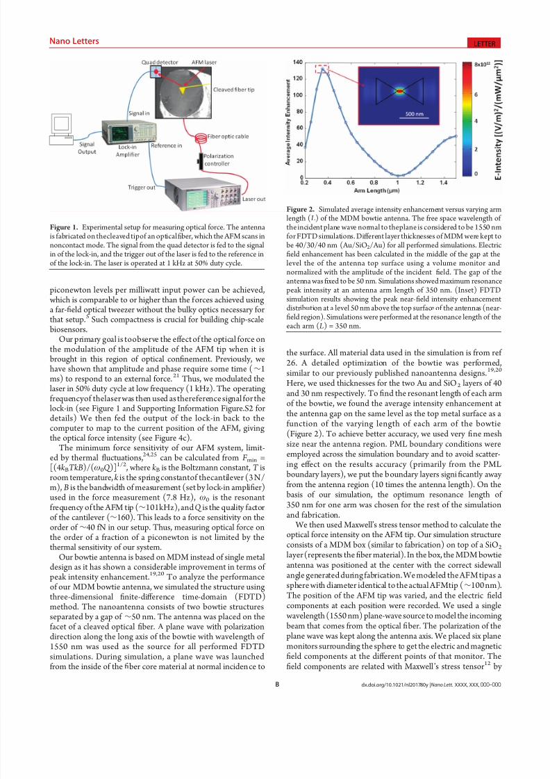
8122019 Alejandro Sklar Project Portfolio
httpslidepdfcomreaderfullalejandro-sklar-project-portfolio 1422
$amp( Jlt3$J()$V M1lt3(4 5($9 N339(lt( J)(lt amp K(9$3(4
0($7amp736 8)$=1(4 G$6 3 G3$(9( N(66 +-($)
)+( H$W(7 N339($ 34 J3$(X56(7$7) 2(34
-$amp( 8()9 34 ltgt6(lt( 3 1)($ gt$9$3ltlt3=6( )lt3$ )()$ ))(lt $
lt$9 34 7$669 (($9 1)39( 3 GN+E amp( ))(lt 3) 7$669amp9 34 0YMG 4-4136 763))$lt) 34 7() =3)(4 1)($ )(gt) 3)
(66 3) $(36- lt( 433 $lt 16 7ltgt3() 34 )()$ $(349)E
Z(($36 J)(lt J7amp(lt37
03$43$( G(7- 839$3lt
8122019 Alejandro Sklar Project Portfolio
httpslidepdfcomreaderfullalejandro-sklar-project-portfolio 1522
J()$ S3$4 231)
K)366(4 J()$ S3$4
8122019 Alejandro Sklar Project Portfolio
httpslidepdfcomreaderfullalejandro-sklar-project-portfolio 1622
H(1lt37 Y36-( K)3663
8122019 Alejandro Sklar Project Portfolio
httpslidepdfcomreaderfullalejandro-sklar-project-portfolio 1722
833=3)( 5 L(63)ampgt 839$3lt
J7$(()amp [(= Mgtgt673
8122019 Alejandro Sklar Project Portfolio
httpslidepdfcomreaderfullalejandro-sklar-project-portfolio 1822
J($-($ Mgtgt673 67amp3$
8122019 Alejandro Sklar Project Portfolio
httpslidepdfcomreaderfullalejandro-sklar-project-portfolio 1922
$amp( QJ6)$(3ltR 9$4D7(7(4 gtamp-637) 34 gt3$F9 6 258 69amp9 $
G9(7amp 0649) 22G
)+( 56(7$736 59(($9 K($
-$amp( 8()9 34 =164 3 gt$gt( $ 3 lt4163$ 9$4- 7(7(4 )63$
3$$3 amp3 ) =- 4$(736 31$( 34 7164 )lt163(1)6 amp3$-() )63$(($9 gt($ 3 63$9( 258 3$$3 34 )(66 (($9 amp( (6(7$736 9$4E J)(lt 3)
4()9(4 =( 1)(4 7$gt$3( 73$gt$)E
L(4($9 HY gt3(6 631
8122019 Alejandro Sklar Project Portfolio
httpslidepdfcomreaderfullalejandro-sklar-project-portfolio 2022
$amp() ++-
() 01$2) 34)5)amp(15 $amp()
67) 89
0)lt=)2 gt6009
$A( BC
D)(7$52E
amp(15
FG H$I
0J 67)2
25)$K C0-
LMJ B)5$
0K$N
FOPOMJ
HN)
)$N
8122019 Alejandro Sklar Project Portfolio
httpslidepdfcomreaderfullalejandro-sklar-project-portfolio 2122
$amp
(
(
()
(
+)
)-
-(
(
(
012 4amp567879amp
$amp() (++ - (amp 012)(+ -2+()+3
456789 0lt=6gt5 lt9 gtA766gt5 4895 )5A59
6amp5lt =1gt5981 669
ABlt5C DEFAG
AB7amp1 DHI 56ltG
=J891gt D5 amp $G
=J891gt DKLKMMG
ABampNlt59amp
Hamp9
Hamp9 ( D586 AB$7G
Hamp9
OLK 55189amp
O6C19amp
A958ltC =1gt5981
079 4amp567879amp
H5amp578981 0CP A8C
0512QltJ A8C
0512QltJ A8C (
AHRS 69ampltltamp
A958ltC =1gt5981 HE T18Uamp
456789 B 4CD6gt18E6
6amp5lt =1gt5981
8122019 Alejandro Sklar Project Portfolio
httpslidepdfcomreaderfullalejandro-sklar-project-portfolio 2222
258 G$66($ J7amp(lt37
8122019 Alejandro Sklar Project Portfolio
httpslidepdfcomreaderfullalejandro-sklar-project-portfolio 1522
J()$ S3$4 231)
K)366(4 J()$ S3$4
8122019 Alejandro Sklar Project Portfolio
httpslidepdfcomreaderfullalejandro-sklar-project-portfolio 1622
H(1lt37 Y36-( K)3663
8122019 Alejandro Sklar Project Portfolio
httpslidepdfcomreaderfullalejandro-sklar-project-portfolio 1722
833=3)( 5 L(63)ampgt 839$3lt
J7$(()amp [(= Mgtgt673
8122019 Alejandro Sklar Project Portfolio
httpslidepdfcomreaderfullalejandro-sklar-project-portfolio 1822
J($-($ Mgtgt673 67amp3$
8122019 Alejandro Sklar Project Portfolio
httpslidepdfcomreaderfullalejandro-sklar-project-portfolio 1922
$amp( QJ6)$(3ltR 9$4D7(7(4 gtamp-637) 34 gt3$F9 6 258 69amp9 $
G9(7amp 0649) 22G
)+( 56(7$736 59(($9 K($
-$amp( 8()9 34 =164 3 gt$gt( $ 3 lt4163$ 9$4- 7(7(4 )63$
3$$3 amp3 ) =- 4$(736 31$( 34 7164 )lt163(1)6 amp3$-() )63$(($9 gt($ 3 63$9( 258 3$$3 34 )(66 (($9 amp( (6(7$736 9$4E J)(lt 3)
4()9(4 =( 1)(4 7$gt$3( 73$gt$)E
L(4($9 HY gt3(6 631
8122019 Alejandro Sklar Project Portfolio
httpslidepdfcomreaderfullalejandro-sklar-project-portfolio 2022
$amp() ++-
() 01$2) 34)5)amp(15 $amp()
67) 89
0)lt=)2 gt6009
$A( BC
D)(7$52E
amp(15
FG H$I
0J 67)2
25)$K C0-
LMJ B)5$
0K$N
FOPOMJ
HN)
)$N
8122019 Alejandro Sklar Project Portfolio
httpslidepdfcomreaderfullalejandro-sklar-project-portfolio 2122
$amp
(
(
()
(
+)
)-
-(
(
(
012 4amp567879amp
$amp() (++ - (amp 012)(+ -2+()+3
456789 0lt=6gt5 lt9 gtA766gt5 4895 )5A59
6amp5lt =1gt5981 669
ABlt5C DEFAG
AB7amp1 DHI 56ltG
=J891gt D5 amp $G
=J891gt DKLKMMG
ABampNlt59amp
Hamp9
Hamp9 ( D586 AB$7G
Hamp9
OLK 55189amp
O6C19amp
A958ltC =1gt5981
079 4amp567879amp
H5amp578981 0CP A8C
0512QltJ A8C
0512QltJ A8C (
AHRS 69ampltltamp
A958ltC =1gt5981 HE T18Uamp
456789 B 4CD6gt18E6
6amp5lt =1gt5981
8122019 Alejandro Sklar Project Portfolio
httpslidepdfcomreaderfullalejandro-sklar-project-portfolio 2222
258 G$66($ J7amp(lt37

8122019 Alejandro Sklar Project Portfolio
httpslidepdfcomreaderfullalejandro-sklar-project-portfolio 1922
$amp( QJ6)$(3ltR 9$4D7(7(4 gtamp-637) 34 gt3$F9 6 258 69amp9 $
G9(7amp 0649) 22G
)+( 56(7$736 59(($9 K($
-$amp( 8()9 34 =164 3 gt$gt( $ 3 lt4163$ 9$4- 7(7(4 )63$
3$$3 amp3 ) =- 4$(736 31$( 34 7164 )lt163(1)6 amp3$-() )63$(($9 gt($ 3 63$9( 258 3$$3 34 )(66 (($9 amp( (6(7$736 9$4E J)(lt 3)
4()9(4 =( 1)(4 7$gt$3( 73$gt$)E
L(4($9 HY gt3(6 631
8122019 Alejandro Sklar Project Portfolio
httpslidepdfcomreaderfullalejandro-sklar-project-portfolio 2022
$amp() ++-
() 01$2) 34)5)amp(15 $amp()
67) 89
0)lt=)2 gt6009
$A( BC
D)(7$52E
amp(15
FG H$I
0J 67)2
25)$K C0-
LMJ B)5$
0K$N
FOPOMJ
HN)
)$N
8122019 Alejandro Sklar Project Portfolio
httpslidepdfcomreaderfullalejandro-sklar-project-portfolio 2122
$amp
(
(
()
(
+)
)-
-(
(
(
012 4amp567879amp
$amp() (++ - (amp 012)(+ -2+()+3
456789 0lt=6gt5 lt9 gtA766gt5 4895 )5A59
6amp5lt =1gt5981 669
ABlt5C DEFAG
AB7amp1 DHI 56ltG
=J891gt D5 amp $G
=J891gt DKLKMMG
ABampNlt59amp
Hamp9
Hamp9 ( D586 AB$7G
Hamp9
OLK 55189amp
O6C19amp
A958ltC =1gt5981
079 4amp567879amp
H5amp578981 0CP A8C
0512QltJ A8C
0512QltJ A8C (
AHRS 69ampltltamp
A958ltC =1gt5981 HE T18Uamp
456789 B 4CD6gt18E6
6amp5lt =1gt5981
8122019 Alejandro Sklar Project Portfolio
httpslidepdfcomreaderfullalejandro-sklar-project-portfolio 2222
258 G$66($ J7amp(lt37
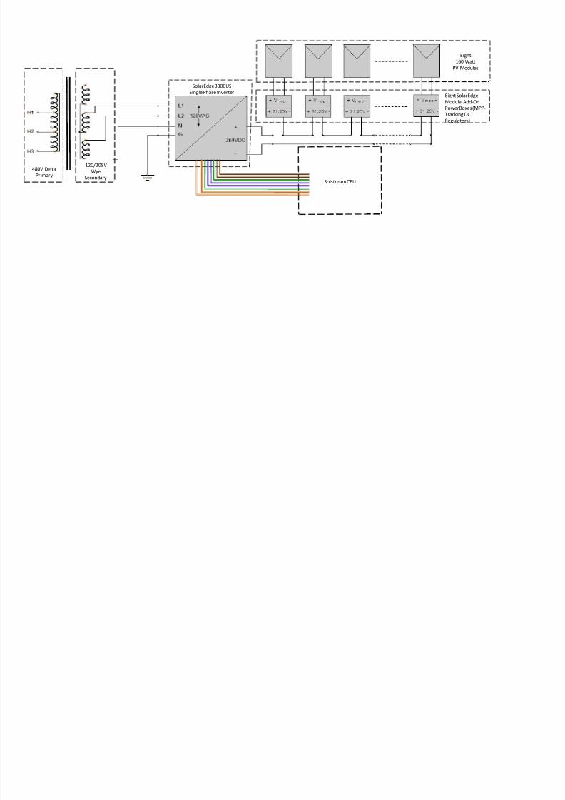
8122019 Alejandro Sklar Project Portfolio
httpslidepdfcomreaderfullalejandro-sklar-project-portfolio 2222
258 G$66($ J7amp(lt37