Embed Size (px)
Citation preview

To learn more about ON Semiconductor, please visit our website at www.onsemi.com
Is Now Part of
ON Semiconductor and the ON Semiconductor logo are trademarks of Semiconductor Components Industries, LLC dba ON Semiconductor or its subsidiaries in the United States and/or other countries. ON Semiconductor owns the rights to a number of patents, trademarks, copyrights, trade secrets, and other intellectual property. A listing of ON Semiconductor’s product/patent coverage may be accessed at www.onsemi.com/site/pdf/Patent-Marking.pdf. ON Semiconductor reserves the right to make changes without further notice to any products herein. ON Semiconductor makes no warranty, representation or guarantee regarding the suitability of its products for any particular purpose, nor does ON Semiconductor assume any liability arising out of the application or use of any product or circuit, and specifically disclaims any and all liability, including without limitation special, consequential or incidental damages. Buyer is responsible for its products and applications using ON Semiconductor products, including compliance with all laws, regulations and safety requirements or standards, regardless of any support or applications information provided by ON Semiconductor. “Typical” parameters which may be provided in ON Semiconductor data sheets and/or specifications can and do vary in different applications and actual performance may vary over time. All operating parameters, including “Typicals” must be validated for each customer application by customer’s technical experts. ON Semiconductor does not convey any license under its patent rights nor the rights of others. ON Semiconductor products are not designed, intended, or authorized for use as a critical component in life support systems or any FDA Class 3 medical devices or medical devices with a same or similar classification in a foreign jurisdiction or any devices intended for implantation in the human body. Should Buyer purchase or use ON Semiconductor products for any such unintended or unauthorized application, Buyer shall indemnify and hold ON Semiconductor and its officers, employees, subsidiaries, affiliates, and distributors harmless against all claims, costs, damages, and expenses, and reasonable attorney fees arising out of, directly or indirectly, any claim of personal injury or death associated with such unintended or unauthorized use, even if such claim alleges that ON Semiconductor was negligent regarding the design or manufacture of the part. ON Semiconductor is an Equal Opportunity/Affirmative Action Employer. This literature is subject to all applicable copyright laws and is not for resale in any manner.

www.fairchildsemi.com
© 2009 飞兆半导体公司 www.fairchildsemi.com
Rev. 1.0.2 • 10/13/13
AN-6300 FAN6300 / FAN6300A / FAN6300H
高度集成的准谐振PWM控制器
摘要
本应用指南介绍使用准谐振PWM控制器的功率转换设计
详细方法,相比传统采用固定开关频率的硬开关转换器
,该设计具有更高的效率、更佳的EMI性能。本应用指
南中根据设计指南设计的具有详细参数的案例,可以演
示控制器性能。
引言
高度集成的FAN6300/A/H PWM控制器的一些特色可以增
强反激式转换器性能。FAN6300/A应用于最大工作频率
低于100kHz的准谐振反激式转换器,而FAN6300H适合
190kHz左右的高频操作。内置的高压(HV)启动电路可提
供更大的启动电流,以减少控制器的启动时间。当VDD
电压超过工作阈值电压,HV启动功能就会立即断开以降
低功耗。内部谷底电压检测器可确保功率系统在宽范围
线路电压下能够以准谐振状态运行,减少开关损耗以最
大限度降低功率MOSFET漏极上的开关电压。
为最大限度地降低待机功耗和提高轻载效率,该器件采
用了专有的绿色模式功能,提供关断时间调制以减小开
关频率,并扩大谷底电压切换范围,以最大限度地降低
开关电压。
FAN6300/A/H控制器提供多种保护功能。逐脉冲电流限
制功能可确保系统具有固定的峰值电流限度,即使发生
短路亦然。一旦反馈环路中出现开路故障,内部保护电
路便会立即终止PWM输出。此外,只要VDD降低到关断阈
值电压以下,该控制器也会禁用PWM输出。栅极输出被
钳制在18V以保护功率MOSFET在栅极-源极出现高压时不
被损坏。而最小tOFF时间限制能防止系统频率过高。如
果DET引脚达到OVP条件,或者内部OTP被触发,功率系
统将进入锁死模式,直到交流电源断开为止。

AN-6300 应用指南
© 2009 飞兆半导体公司 www.fairchildsemi.com
Rev. 1.0.2 • 10/13/13 2
6
4
8
7
2
1
5
3
HV
FB
DET
GATE
CSGND
VDD
NC
VAC
+
-
Vo
图 1. 基本准谐振转换器
CS
8 6
2
3
1
4 7
5
0.3V
DRV
GND
VDD
Two Steps
UVLO
16V/10V/8V
Internal
Bias
Latched
18V
GATE
DET
FB
NC
HV
Latched
4.2V
2R
R
Soft-Start
5ms
PWM
Current Limit
IDET
Internal
OTPLatched
S/H
Blanking
Circuit
tOFF-MIN
(8µs/38µs)
IDET
5V
DET OVP
2.5V
tOFF
Blanking
(4µs)
Q
QSET
CLR
S
R
FB OLPTimer
55ms
Over-Power
Compensation
VDET
Starter
30µs
Latched
Valley
Detector
0.3V
27V
OVP
VDET
IHV
1st
Valley
tOFF-MIN
+9µs
2ms
(3µs/13µs)
for H version
tOFF-MIN +5µs
for H version
(1.5µs) for H version
图 2. 功能框图

AN-6300 应用指南
© 2009 飞兆半导体公司 www.fairchildsemi.com
Rev. 1.0.2 • 10/13/13 3
变压器初级端电感设计步骤
在本节中,使用作为参考的图 1的原理图对设计步
骤进行介绍。
[a] 定义系统规格
线路电压范围(Vin,min和Vin,max)
最大输出功率(Po)。
输出电压(Vo)和最大输出电流(Io)
估算效率(η)
必须先估算功率转换效率,才能计算最大输入功率。
在NB适配器应用中,典型效率为85%~90%。
得到效率估算值后,最大输入功率可由下式给出:
o
in
PP =
η (1)
[b] 估算反映输出电压
图 3显示的是准谐振反激式转换器的漏极电压典型
波形。MOSFET关断时,直流链路电压(Vo)、输出电压
(Vo)和肖特基二极管正向压降(Vd)反映到初级端,并
施加在MOSFET上。MOSFET上的最大标称电压(Vds)为:
ds,max in,max o dV V + n V +V= ( ) (2)
其中,变压器初级端到次级端的匝数比定义为n和Vds,由等式2指定。
通过增加n的值,可减少MOSFET的容性开关损耗和导
通损耗。但是,这样做会增加MOSFET上的电压应力,
如图 3所示。因此,确定n时,需在MOSFET电压裕量
和效率之间作出权衡取舍。通常认为Vds的关断电压尖
峰为100V,因此Vds,max设计为490~550V左右(MOSFET额
定电压的75~85%)。
[c] 确定变压器初级端电感(LP)
图 4显示的是QR转换器中MOSFET漏电流(Ids)、次级
端二极管电流(Id)和MOSFET漏电压(Vds)的典型波形。
在tOFF持续期间,电流流过次级端整流二极管。当Id下
降到零时,Vds开始随MOSFET有效输出电容和初级端电
感(LP)之间的谐振频率下降。为实现最少的开关损
耗,FAN6300/A/H设计为当Vds 到达其最小电压Vin-n(Vo+Vd)时使MOSFET导通。
Vin
+
-
Vo
+
-
Coss Vds
+
-
+
-
Vds
Vin,max
n(Vo+Vd)
Vds
0V
n(Vo+Vd)
n(Vo+Vd)
n(Vo+Vd)
+ -Vd
n(Vo+Vd)
n:1
图 3. QR工作时MOSFET漏电压的典型波形
Ids
Id
Vds
Vin
Vin+n(Vo+Vd)
tON tOFF tF
TS
n(Vo+Vd)
Vin-n(Vo+Vd)
n(Vo+Vd)
IinIds
pk
DTs
图 4. QR工作时的典型波形

AN-6300 应用指南
© 2009 飞兆半导体公司 www.fairchildsemi.com
Rev. 1.0.2 • 10/13/13 4
确定初级端电感(LP)之前应先确定下列变量:
最小开关频率(fs,min): 最小输入电压和满载条
件下可实现最大平均输入电流。同时,在QR工作
期间,开关频率具有最小值。
MOSFET漏电压的下降时间(tf): 如图 4所示,
MOSFET漏电压下降时间为MOSFET有效输出电容和
初级端电感谐振周期的一半。若增加的谐振电容
与Coss并联连接,可增加 tf ,同时减少EMI。然
而,这会迫使开关损耗增加。NB适配器应用的tf
典型值约为0.5~1μs。
确定fs,min和tf之后, 最大占空比可由下式计算得出:
o d
max s,min f
o d in
n V +VD (1 - f t )
n V +V +V
( )=
( ) (3)
其中,Vin,min在低压线路和满载条件下指定。根据等式
1,最大平均输入电流Iin,max可由下式确定:
o o
in,max
in,min
V II
V η= (4)
根据图 3,Iin,max可由下式获得:
pk
in,max max ds,max
1I D I
2 (5)
Ids,maxpk可由下式确定:
pk in,min max
ds,max
m s,min
V DI
L f (6)
在等式5中,以等式6替换Ids,maxpk,然后结合等式4和等
式5获得LP:
2
in,min max
P
in s,min
(V DL
2P f
)= (7)
其中,Pin和Dmax分别在等式1和等式3中指定,fs,min是最
小开关频率。
一旦确定LP,标称工作条件下的MOSFET RMS电流值可
由下式获得:
rms peakmax
ds,max ds,max
DI I
3= (8)
[d] 确定合适的磁芯和初级端最小匝数
设计变压器时,应考虑正常工作条件下的最大通量密
度摆幅(Bmax)。正常工作时的最大磁通密度摆幅与磁芯
的磁滞损耗有关,瞬态时的最大磁通密度摆幅与磁芯
饱和有关。
根据法拉第定理,变压器初级端最小匝数可由下式给
出:
pk
6P ds,max
P,min
max e
L IN 10
B A= (9)
其 中 ,
LP 由 等 式 7 指 定 ;
Ids,maxpk 是 由 等 式 6 指 定 的 峰 值 漏 电 流 ;
Ae 是 磁 芯 横 截 面 积 ( 单 位 : mm2 ) ;
Bmax是最大通量密度摆幅(单位:特斯拉)。
通常Bmax可以选用0.25~0.30 T。
确定辅助绕组的匝数
辅助绕组匝数(Na)可由下式获得:
DD D1
a
o d
V +VN =
V +V (10)
其中:
VDD 是 VDD 引 脚 的 工 作 电 压 ;
VD1 是 D1 正 向 压 降 ( 见图 5 ) ;
Vo 和Vd可由等式2确定。
AN-6300 应用指南
© 2009 飞兆半导体公司 www.fairchildsemi.com
Rev. 1.0.2 • 10/13/13 5
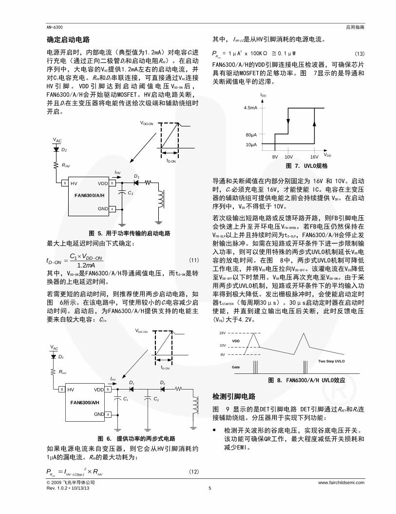
确定启动电路
电源开启时,内部电流(典型值为1.2mA)对电容C1进
行充电(通过正向二极管D2和启动电阻RHV)。在启动
序列中,大电容的VAC提供1.2mA左右的启动电流,并
对C1电容充电。RHV和D2串联连接,可直接通过VAC连接
HV引脚。 VDD引脚达到启动阈值电压 VDD-ON 后,
FAN6300/A/H会开始驱动MOSFET。HV启动电路关断,
并且D1在主变压器将电能传送给次级端和辅助绕组时
开启。
8 6
4
HV VDD
GND
FAN6300/A/H
VAC
D2
RHV
IHVD1
C1
tD-ON
VDD-ON
图 5. 用于功率传输的启动电路
最大上电延迟时间由下式确定:
mA
VCt ONDD
OND2.1
1
(11)
其中,VDD-ON是FAN6300/A/H导通阈值电压,而tD-ON是转
换器的上电延迟时间。
若需更短的启动时间,则推荐使用两步启动电路,如
图 6所示。在该电路中,可使用较小的C1电容减少启
动时间。启动后,为FAN6300/A/H提供支持的电能主
要来自较大电容:C2。
8 6
4
HV VDD
GND
FAN6300/A/H
VAC
D2
RHV
IHV
D1
C1
tD-ON
VDD-ON
C2
D2
图 6. 提供功率的两步式电路
如果电源电流来自变压器,则它会从HV引脚消耗约
1µA的漏电流。RHV的最大功耗为:
HV
2
R HV -LC(typ.) HVP I R (12)
其中,IHV-LC是从HV引脚消耗的电源电流。
HVR
P = 1μA2 x 100KΩ 0.1μW (13)
FAN6300/A/H的VDD引脚连接电压检波器,可确保芯片
具有驱动MOSFET的足够功率。图 7显示的是导通和
关断阈值电平的迟滞。
IDD
4.5mA
VDD8V 10V 16V
80μA
10μA
图 7. UVLO规格
导通和关断阈值在内部分别固定为 16V 和 10V。启动
时,C1必须充电至 16V,才能使能 IC。电容在主变压
器的辅助绕组可提供电能之前会持续提供 VDD。在启动
序列中,VDD不得低于 10V。
若次级输出短路电路或反馈环路开路,则FB引脚电压
会快速上升至开环电压VFB-OPEN。若FB电压仍然保持在
VFB-OLP以上并且持续时间为tD-OLP,FAN6300/A/H会停止发
射输出脉冲。如需在短路或开环条件下进一步限制输
入功率,则可以使用特殊的两步式UVLO机制延长VDD电
容的放电时间。在图 8中,两步式UVLO机制可降低
工作电流,并将VDD电压拉向VDD-OFF。该灌电流在VDD降低
至VDD-OFF以下时禁用。VDD电压再次充电至VDD-ON。由于采
用两步式UVLO机制,短路或开环条件下的平均输入功
率得到极大降低。发出栅极脉冲时,会使能启动定时
器tSTARTER(每周期30μs)。30μs启动定时器在启动时
使能,并直到建立输出电压后关断,此时反馈电压
(VFB)大于4.2V。
Two Step UVLO
Gate
VDD
16V
10V
8V
图 8. FAN6300/A/H UVLO效应
检测引脚电路
图 9 显示的是DET引脚电路 DET引脚通过RDET和RA连
接辅助绕组。分压器用于实现下列功能:
检测开关波形的谷底电压,实现谷底电压开关。
该功能可确保QR工作,最大程度减低开关损耗和
减少EMI。

AN-6300 应用指南
© 2009 飞兆半导体公司 www.fairchildsemi.com
Rev. 1.0.2 • 10/13/13 6
产生失调,补偿峰值限流的阈值电压,提供恒定
的功率限值。当PWM信号使能时,产生的失调与
输入电压相一致。
电压比较器和2.5V基准电压提供输出OVP保护。
分压比可确定在哪个输出电压电平处停止栅极信
号。
6
1DETVDD
RDET
RA
VAUX
+
-
图 9. 检测引脚选择
首先,确定分压电阻的分压比。分压比可确定在哪个
输出电压电平处停止栅极信号。在图 10中,采样电
压VS为:
A A
S O
S DET A
N RV V
N R + R<2.5V (14)
其中,NA是辅助绕组的匝数,NS是次级绕组的匝数。
图 11显示的是使用辅助绕组检测 Vo 时的输出电压
OVP 检测模块。正常条件下,VS 设计为低于 2.5V。VS
标称电压设计为基准电压(2.5V)的 80%左右,因此 VS
的建议值为 1.9V~2.1V。在关断序列之后,输出过压
保护根据采样电压的大小而工作。4μs 屏蔽时间可忽
略漏电感振铃。如果 DET 引脚触发 OVP 条件,或者内
部 OTP 被触发,功率系统将进入锁存模式,直到交流
电源断开为止。
VDET
0V
tOFF Blanking time
Sampling Here
VS
图 10. 关断序列之后4µs(H版本为1.5µs)消隐时间
结束后的电压采样。
1
DET
S/H
DET OVP
tOFF
Blanking
(4µs)
VDET
Latched
0.3V
2.5V
5V
+
-
Vo
RA
RDET
To VDD
(1.5µs) for H version
图 11. 输出电压OVP检测模块
一旦次级端开关电流放电至零电平,便在DET引脚上
生成一个谷底信号。通过检测切换波形的波谷电压,
实现谷底电压开起 若辅助绕组VAUX上的电压为负,(
如图 9中的定义),则DET引脚电压箝位至0.3V。建
议RDET的范围为150k至220k,以便实现谷底电压开关。
确定平台电压VS(图 10)之后,可通过等式14计算
RA 。
图 12显示的是FAN6300/A/H的内部谷底检测模块。
内部定时器(最小tOFF时间)可防止系统频率过高。首
次谷底开关在最小tOFF时间8μs(H版本为3µs)计时后
激活。图 13显示的是具有首次谷底开关的典型漏电
压波形。
1
DET
tOFF-MIN
(8µs/38µs)
5V
Valley Detector
VDET1 st
Valley
tOFF- MIN
+9µs
VFB
To SR F/F
0.3V
0.3V
RA
RDET
To VDD
VAUX
+
-
Vin
(3µs/13µs)
for H version
tOFF-MIN +5µs
for H version
图 12. 谷底检测模块

AN-6300 应用指南
© 2009 飞兆半导体公司 www.fairchildsemi.com
Rev. 1.0.2 • 10/13/13 7
图 13. 第一谷底开关
专有绿色模式功能提供可在轻负载条件下线性降低开
关频率的关断时间调制。选用电压反馈环路的VFB信号
作为参考电压。在图 14中,一旦VFB低于2.1V,tOFF-MIN
时间便会随VFB的降低而线性增加。只有当tOFF-MIN时间结
束时,谷底电压检测信号才会开始。因此,谷底检测
电路在tOFF-MIN时间结束前一直处于激活状态,这样可降
低开关频率,同时扩展谷底电压开关。在极轻负载条
件下,tOFF-MIN结束后,可能无法检测谷底电压。此时,
内部tTIME-OUT信号会在9μs(H版本为5µs)延迟后启动
一个新周期。图 15和图 16显示的是两种不同的情
况。
tOFF-MIN
VFB1.2V 2.1V
2ms
38/13μs
8/3μs
图 14. VFB与 tOFF-MIN的关系曲线
图 15. 扩展波谷电压检测模式下QR工作波形
图 16. 内部tTIME_OUT在未能检测谷底电压后会启动新周
期(FAN6300H为5μs延迟)
图 17显示的是VFB与 PWM频率的关系曲线,其中fs,min是最
小输入电压和满载条件下的最小开关频率,fs,max是首
次谷底开关期间的最大开关频率,fs,g是9μs(H版本
为5µs)定时器使能时的最小频率。输出负载逐渐小
于最大负载时,VFB会变得更低。当VFB低于2.1V时,绿色模
式功能激活;从而tOFF时间得到线性扩展。反激式转换器被
迫进入非连续导通模式(DCM);因此,开关频率fs可在
MOSFET漏电压于进一步扩展的谷底电压(第2个谷底
、第3个谷底、第4个谷底、第5个谷底,以此类推)
处开关时降低。 fs,g高于20kHz,以防音频噪声。 一
旦转换器进入深度DCM模式,VFB便低于1.2V。同时,
2ms定时器tSTARTER使能,fs约为500Hz,以便节能。
Switching frequency (Hz)
VFB
1.2V 2.1V
fs,min
fs,max
20k
fs,g
VFB,max
2k
图 17. VFB与 开关频率的关系曲线
RDET可确定扩展谷底开关能力。RDET典型值为150k-
220kΩ。较小的RDET值可增强扩展谷底开关能力,并进
而能开关扩展谷底电压。在不同应用中,MOSFET漏电
压下降时间(tf,见图 4)可能会使谷底开关电压不
精确。调节RDET值,或在DET引脚和GND引脚之间连接一
个CA电容,这样可能会对谷底开关电压很有用。CA的
建议值低于22pF。
RDET还会影响高压/低压线路恒定功率限制。为了补偿
交流输入宽范围的波动变化,DET引脚产生失调电压
来补偿峰值限流的阀值电压,以此提供恒定的功率限
度。当PWM信号使能时,产生的失调与输入电压相一
致。这导致在高电源电压输入时比低电压输入时的电

AN-6300 应用指南
© 2009 飞兆半导体公司 www.fairchildsemi.com
Rev. 1.0.2 • 10/13/13 8
流限度更低。在固定负载条件下,RDET的值越高,CS限
值也越高。
设计反馈控制
FAN6300/A/H设计用于峰值电流模式控制。通过电流
感测电阻RS可在外部实现电流-电压转换。正常工作
下,FB电平可控制峰值电感电流IPK:
S
FBPK
R
VI
3
2.1 (15)
其中,VFB是FB引脚电压。
当VFB低于1.2V时,会使能启动定时器tSTARTER(每周期为
500μs)。
图 18是一种典型的反馈电路,主要由分流稳压器和
光电耦合器组成。R1和R2构成用于输出电压调节的分
压器。R3和C1针对控制环路补偿进行了调节。将小数
值RC滤波器(如RFB =10Ω、CFB = 10nF)放置在FB引
脚和GND之间,可进一步提高稳定性。FB引脚的最大
拉电流为1.2 mA。该光耦必须能够灌入该电流,才能
在空载时拉低FB 电平。偏置电阻Rb的电阻值可由下式
确定:
O D Z
b
V -V -VK
R≥ 1.2mA (16)
其中,
VD是光耦的压降,约为 1.2V;
VZ是最小工作电压,对于分流调节器为
2.5V;
K 是光电耦合器的电流传输比(CTR)。
对于输出电压 VO = 5V 且 CTR=100%,Rb最大值为
860Ω。
FB
Vo
R1
R2
Rb
R3C1
RFB
CFB
图 18. 反馈电路
屏蔽时间(LEB) 电流感测电阻RS上存在与MOSFET电流成比例的电压信
号。每次开启MODFET,二极管反向恢复特性、MOSFET
输出电容和二极管都会感应一个尖峰,该效应会无可
避免地出现在感测信号中。引入约300ns的前沿消隐
时间是为了避免尖峰提前关断MOSFET。在SENSE引脚
和 RS之间只需使用小数值 RC滤波器(如100Ω +
470pF) 建议针对RS采用非感性电阻。
GATE
CSBlanking
Circuit
FAN6300/A/H
RS
图 19. 导通尖峰

AN-6300 应用指南
© 2009 飞兆半导体公司 www.fairchildsemi.com
Rev. 1.0.2 • 10/13/13 9
输出驱动器/软驱动
输出级采用快速图腾柱驱动器,可直接驱动 MOSFET
栅极。它还采用了电压钳位齐纳二极管,保护 MOSFET
不受非预期过驱电压的损坏。输出电压箝位在 18V。
内部下拉电阻用于避免启动前的栅极浮空状态。通过
集成电路控制开关开启时上升时间的压摆率,可能无
需外部电阻 RG就可降低开关噪声,提高电磁干扰(EMI)
性能。
ON/OFF
Driver
FAN6300/A/H
RG
VDD
GATE
18V
图 20. 栅极驱动
变压器结构
漏电感影响
图 21显示的是MOSFET漏极端子的实际波形。关断
MOSFET时,会因变压器漏电感而在漏极端子上产生电
压尖峰(Vspike)。漏电感计算起来并非那么容易,但通
过三明治绕法使其最小 同时,辅助绕组上的电压波
形与MOSFET漏极端子上的波形相似。这些尖峰电压会
对VDD电容产生额外的电能,从而破坏VDD电压和输出电
压之间的关系。
Vds
0V
Vspike
Vin
图 21. MOSFET漏电压波形
通常采用的有以下两种变压器结构:
A类结构:
A类结构是一种交错多层绕组方法。电源常用的结构
是把次级绕组夹在初级端两半边之间,尤其当输出功
率很大时。辅助绕组通过初级绕组之间厚度的增加而
位于顶层。该操作可降低漏电感,同时增加初级绕组
和次级绕组之间的耦合。它还可以提高转换效率,减
少因变压器漏电感而引起的MOSEFT上的电压尖峰。但
是,它能轻松反映辅助绕组上的电压尖峰,使轻负载
和重负载条件下的VDD电压出现较大偏差。
B类结构:
另一种传感器结构采用堆栈式绕组方法,通常用于输
出功率较小的开关电源。相比A类结构,该方法在初
级绕组和次级绕组之间的耦合效果较差,因此,
MOSFET上的电压尖峰更高,转换效率更低。
图 22显示的是针对交错多层绕组修改的A类结构。
辅助绕组和次级绕组位于初级绕组两半边之间。采用
这种方法,可在轻负载和重负载条件下实现更小的VDD
电压偏差。同时,输出电压OVP电平也更精确。因
此,建议用于适配器的变压器结构如图 22所示。
Winding
Primary
Winding
Secondary
Winding
(Insulated)
Primary
Winding
Auxiliary
图 22. 交错多层绕组结构

AN-6300 应用指南
© 2009 飞兆半导体公司 www.fairchildsemi.com
Rev. 1.0.2 • 10/13/13 10
实验室说明
更改或焊接/去焊接电源之前,可通过外部泄放电阻
对初级电容放电。否则,在此过程中PWM IC可能会被
外部高电压所破坏。
该器件对静电放电(ESD)敏感。为了提高产量,应依
据 ANSI ESD S1.1、ESD S1.4、ESD S7.1、ESD STM
12.1 以及 EOS/ESD S6.1 标准,对生产线采取 ESD
防护。
印刷电路板布局
电流、电压和开关频率使印刷电路板布局和设计成
为非常重要的问题。良好的PCB布局可最大限度地
减少过多的电磁干扰(EMI),并可防止电源在浪涌
/ESD测试期间中断。
布局指南:
要实现更好的EMI性能并减少线路频率纹波,桥
式整流器的输出应当首先连接到电容Cbulk,然后
连接到开关电路。
初级端高频电流环路为 Cbulk – 变压器 –
MOSFET – RS – Cbulk。该电流环路包围的面积
应尽可能的小。保持走线(特别是4→1)尽量
短、直、宽。与MOSFET漏极和RCD缓冲器有关的
高压走线应远离控制电路,以防止不必要的干
扰。如果针对MOSFET使用了散热片,则建议将
该散热片接地。
如3所示,应首先连接控制电路的地线,然后再
连接其他电路。
如2所示,由变压器辅助绕组(D1和C1)封闭的
区域也应小一些。将C1靠近FAN6300/A/H放置,
以实现良好去耦。
针对接地连接有两种各有利弊的建议:
GND3→2→4→1: 避免感测信号和常见阻抗干扰的可
行方法。
GND3→2→1→4: ESD测试时,若电源无法接地,则该
路径更好。ESD放电电荷自次级端通过变压器杂散电
容首先到达GND2。然后,电荷从GND2 到达GND1,再
返回市电电源处。控制电路不可放置在放电路径上。
针对共模扼流圈进行尖端放电可降低高频阻抗,增加
ESD抗扰度。
如果需要一个Y电容连接初级端和次级端,可将此Y电
容连接至Cbulk的正极(VDC)。如果该Y电容连接初级端
GND,则应将其直接连接Cbulk (GND1)的负极。该Y电
容的尖端放电同样有助于抑制ESD。然而,根据安全
要求,两端点之间的爬电距离应当至少为5mm。
Cbulk
VDD
DET
CS
GATE
HV
FB
GND
FAN6300/A/H
Vdc
Vac
Common mode
choke
RDET
RA
C1
RHV
RG
RSRfCf
RFB
CFB
Y-cap
1
2
34 5
图 23. 布局思路

AN-6300 应用指南
© 2009 飞兆半导体公司 www.fairchildsemi.com
Rev. 1.0.2 • 10/13/13 11
设计范例
本节介绍使用QR PWM控制器FAN6300/A/H和临界导通模
式PFC控制器FAN6961的90W (19V/4.74A)适配器设计示
例。PFC输出电压在低交流输入电压时为260V,在高交
流输入电压时为400V。根据技术规格,所有的关键元件
都经过了处理,并且给出了最终的测量结果。
表 1. 系统指标
输入
输入电压范围 90~264VAC
线路频率范围 47~63Hz
输出
输出电压(Vo) 19V
输出功率(Po) 90W
最小开关频率(fs,min) 50kHz
根据设计准则,关键参数的计算与总结如表 2所示。
表 2. 关键系统参数
Dmax 0.327 n 6.8
Ids,maxpk 2.429A LP 700µH
Vin,min 260V Vin,max 400V
Vds,max 533.28V Vd 0.6V
tf 0.6μs η 0.87
NP 34T NS 5T
NAUX 4T
6
4
8
7
2
1
5
3
HV
FB
DET
GATE
CSGND
VDD
NC
PFC STAGE
C1
+
-
Vo
EMI
FilterAC
Input
L
N
R1
C6
C5
C4
C3
C12
C2
C11
C7 C9
R2
R3
R4
R5
R6
R7
R8
R11
R12
R14
R13
R10
L1
D6
D2
D5
D3D4
D1
Q1
C13
IC1
FAN6300/A/H
IC2
IC3
BD1
C8 R9C10
图 24. 完整电路图

AN-6300 应用指南
© 2009 飞兆半导体公司 www.fairchildsemi.com
Rev. 1.0.2 • 10/13/13 12
表 3. 材料单
部件 数值 备注 部件 数值 备注
电阻 MOSFET
R1 100k 1/4W Q1 FDP15N65 15A/650V
R2 68k 2W 电感
R3 0 1/4W L1 3µH
R4 180k 1/4W IC
R5 27k 1/4W IC1 FAN6300/A/H
R6 10 1/4W IC2 PC817
R7 100 1/4W IC3 TL431
R8 0.2 2W 二极管
R9 47k 1/4W D1 0.5A/600V
R10 33 1/2W D2 BYV95C
R11 220 1/4W D3 FR103
R12 68k 1/4W D4 1N4148
R13 10k 1/4W D5 20A/100V 肖特基二极管
R14 1.6k 1/4W D6 20A/100V 肖特基二极管
BD1 4A/600V 桥式二极管
电容
C1 68µF 450V C12 22nF
C2 3.3nF 630V C13 222P/250V Y电容
C3 47µF 50V
C4 10µF 50V
C5 470pF
C6 47nF
C7 1000µF 25V
C8 470µF 25V
C9 470µF 25V
C10 470µF 25V
C11 1nF 1kV

AN-6300 应用指南
© 2009 飞兆半导体公司 www.fairchildsemi.com
Rev. 1.0.2 • 10/13/13 13
相关数据表
FAN6300 — 高度集成的准谐振电流PWM控制器
DISCLAIMER FAIRCHILD SEMICONDUCTOR RESERVES THE RIGHT TO MAKE CHANGES WITHOUT FURTHER NOTICE TO ANY PRODUCTS HEREIN TO IMPROVE RELIABILITY, FUNCTION, OR DESIGN. FAIRCHILD DOES NOT ASSUME ANY LIABILITY ARISING OUT OF THE APPLICATION OR USE OF ANY PRODUCT OR CIRCUIT DESCRIBED HEREIN; NEITHER DOES IT CONVEY ANY LICENSE UNDER ITS PATENT RIGHTS, NOR THE RIGHTS OF OTHERS. LIFE SUPPORT POLICY FAIRCHILD’S PRODUCTS ARE NOT AUTHORIZED FOR USE AS CRITICAL COMPONENTS IN LIFE SUPPORT DEVICES OR SYSTEMS WITHOUT THE EXPRESS WRITTEN APPROVAL OF THE PRESIDENT OF FAIRCHILD SEMICONDUCTOR CORPORATION. As used herein: 1. Life support devices or systems are devices or systems
which, (a) are intended for surgical implant into the body, or (b) support or sustain life, or (c) whose failure to perform when properly used in accordance with instructions for use provided in the labeling, can be reasonably expected to result in significant injury to the user.
2. A critical component is any component of a life support device or system whose failure to perform can be reasonably expected to cause the failure of the life support device or system, or to affect its safety or effectiveness.
www.onsemi.com1
ON Semiconductor and are trademarks of Semiconductor Components Industries, LLC dba ON Semiconductor or its subsidiaries in the United States and/or other countries.ON Semiconductor owns the rights to a number of patents, trademarks, copyrights, trade secrets, and other intellectual property. A listing of ON Semiconductor’s product/patentcoverage may be accessed at www.onsemi.com/site/pdf/Patent−Marking.pdf. ON Semiconductor reserves the right to make changes without further notice to any products herein.ON Semiconductor makes no warranty, representation or guarantee regarding the suitability of its products for any particular purpose, nor does ON Semiconductor assume any liabilityarising out of the application or use of any product or circuit, and specifically disclaims any and all liability, including without limitation special, consequential or incidental damages.Buyer is responsible for its products and applications using ON Semiconductor products, including compliance with all laws, regulations and safety requirements or standards,regardless of any support or applications information provided by ON Semiconductor. “Typical” parameters which may be provided in ON Semiconductor data sheets and/orspecifications can and do vary in different applications and actual performance may vary over time. All operating parameters, including “Typicals” must be validated for each customerapplication by customer’s technical experts. ON Semiconductor does not convey any license under its patent rights nor the rights of others. ON Semiconductor products are notdesigned, intended, or authorized for use as a critical component in life support systems or any FDA Class 3 medical devices or medical devices with a same or similar classificationin a foreign jurisdiction or any devices intended for implantation in the human body. Should Buyer purchase or use ON Semiconductor products for any such unintended or unauthorizedapplication, Buyer shall indemnify and hold ON Semiconductor and its officers, employees, subsidiaries, affiliates, and distributors harmless against all claims, costs, damages, andexpenses, and reasonable attorney fees arising out of, directly or indirectly, any claim of personal injury or death associated with such unintended or unauthorized use, even if suchclaim alleges that ON Semiconductor was negligent regarding the design or manufacture of the part. ON Semiconductor is an Equal Opportunity/Affirmative Action Employer. Thisliterature is subject to all applicable copyright laws and is not for resale in any manner.
PUBLICATION ORDERING INFORMATIONN. American Technical Support: 800−282−9855 Toll FreeUSA/Canada
Europe, Middle East and Africa Technical Support:Phone: 421 33 790 2910
Japan Customer Focus CenterPhone: 81−3−5817−1050
www.onsemi.com
LITERATURE FULFILLMENT:Literature Distribution Center for ON Semiconductor19521 E. 32nd Pkwy, Aurora, Colorado 80011 USAPhone: 303−675−2175 or 800−344−3860 Toll Free USA/CanadaFax: 303−675−2176 or 800−344−3867 Toll Free USA/CanadaEmail: [email protected]
ON Semiconductor Website: www.onsemi.com
Order Literature: http://www.onsemi.com/orderlit
For additional information, please contact your localSales Representative
© Semiconductor Components Industries, LLC