Embed Size (px)
Citation preview
Samsung Electronics
LH351B (3535)
Application Note rev1.0
(New : 4. July. 2014)
2
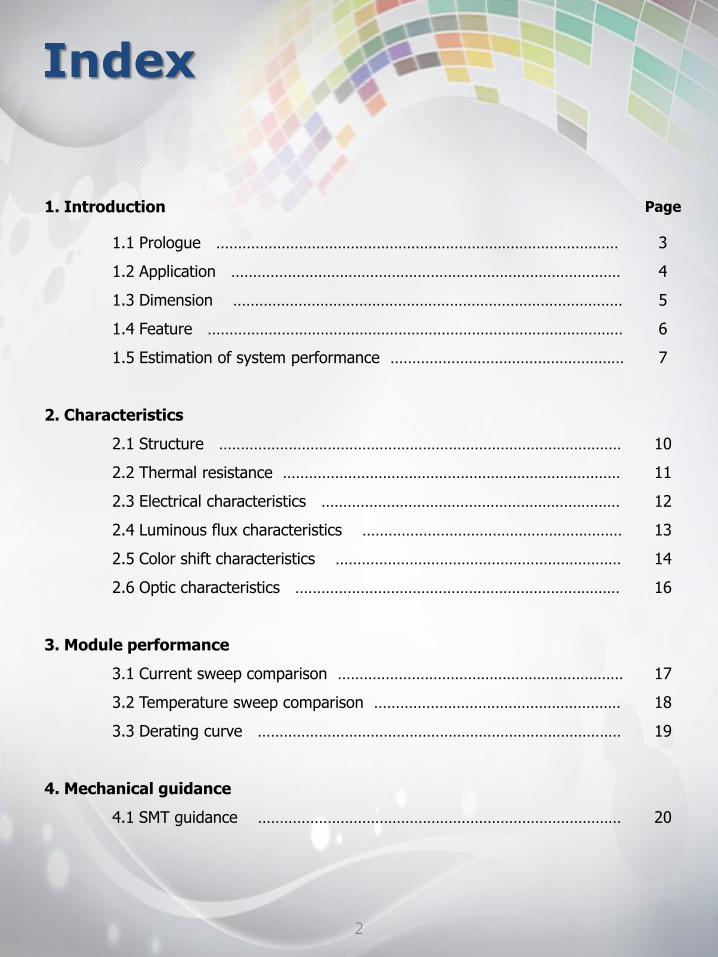
1. Introduction Page
1.1 Prologue ………………………………………………………………………………… 3
1.2 Application ……………………………………………………………………………… 4
1.3 Dimension ……………………………………………………………………………… 5
1.4 Feature …………………………………………………………………………………… 6
1.5 Estimation of system performance ……………………………………………… 7
2. Characteristics
2.1 Structure ………………………………………………………………………………… 10
2.2 Thermal resistance …………………………………………………………………… 11
2.3 Electrical characteristics …………………………………………………………… 12
2.4 Luminous flux characteristics …………………………………………………… 13
2.5 Color shift characteristics ………………………………………………………… 14
2.6 Optic characteristics ………………………………………………………………… 16
3. Module performance
3.1 Current sweep comparison ………………………………………………………… 17
3.2 Temperature sweep comparison ………………………………………………… 18
3.3 Derating curve ………………………………………………………………………… 19
4. Mechanical guidance
4.1 SMT guidance ………………………………………………………………………… 20
Index
1.1 Prologue
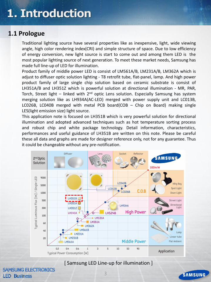
Traditional lighting source have several properties like as inexpensive, light, wide viewing angle, high color rendering index(CRI) and simple structure of space. Due to low efficiency of energy conversion, new light source is start to come out and among them LED is the most popular lighting source of next generation. To meet these market needs, Samsung has made full line-up of LED for illumination. Product family of middle power LED is consist of LM561A/B, LM231A/B, LM362A which is adjust to diffuser optic solution lighting - T8 retrofit tube, flat-panel, lamp. And high power product family of large single chip solution based on ceramic substrate is consist of LH351A/B and LH351Z which is powerful solution at directional illumination - MR, PAR, Torch, Street light – linked with 2nd optic Lens solution. Especially Samsung has system merging solution like as LH934A(AC-LED) merged with power supply unit and LC013B, LC026B, LC040B merged with metal PCB board(COB – Chip on Board) making single LES(light emission size) light source. This application note is focused on LH351B which is very powerful solution for directional illumination and adopted advanced techniques such as hot temperature sorting process and robust chip and white package technology. Detail information, characteristics, performances and useful guidance of LH351B are written on this note. Please be careful these all data and graphs are made for designer reference only, not for any guarantee. Thus it could be changeable without any pre-notification.
3
[ Samsung LED Line-up for illumination ]
1.2 Application
4
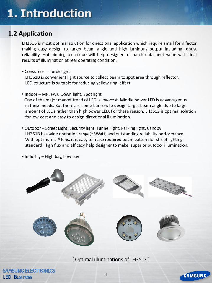
LH351B is most optimal solution for directional application which require small form factor making easy design to target beam angle and high luminous output including robust reliability. Hot binning technique will help designer to match datasheet value with final results of illumination at real operating condition. • Consumer – Torch light LH351B is convenient light source to collect beam to spot area through reflector. LED structure is suitable for reducing yellow ring effect. • Indoor – MR, PAR, Down light, Spot light One of the major market trend of LED is low-cost. Middle power LED is advantageous in these needs. But there are some barriers to design target beam angle due to large amount of LEDs rather than high power LED. For these reason, LH351Z is optimal solution for low-cost and easy to design directional illumination. • Outdoor – Street Light, Security light, Tunnel light, Parking light, Canopy LH351B has wide operation range(~5Watt) and outstanding reliability performance. With optimum 2nd lens, it is easy to make required beam pattern for street lighting standard. High flux and efficacy help designer to make superior outdoor illumination. • Industry – High bay, Low bay
[ Optimal illuminations of LH351Z ]
1.3 Dimension
5
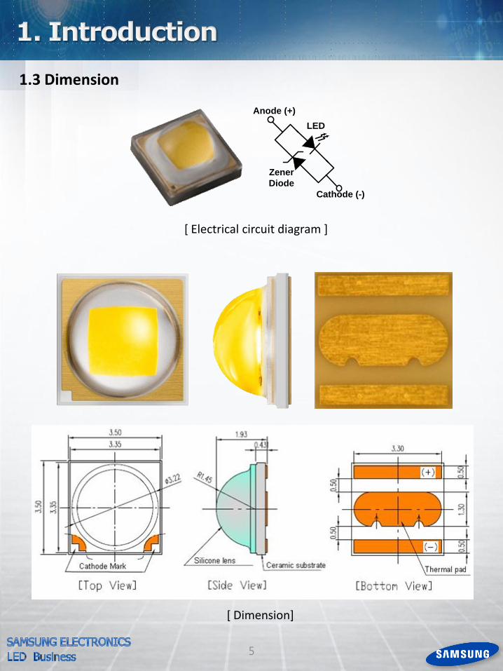
Anode (+)
Cathode (-)
LED
Zener
Diode
[ Electrical circuit diagram ]
[ Dimension]
1.4 Feature
6
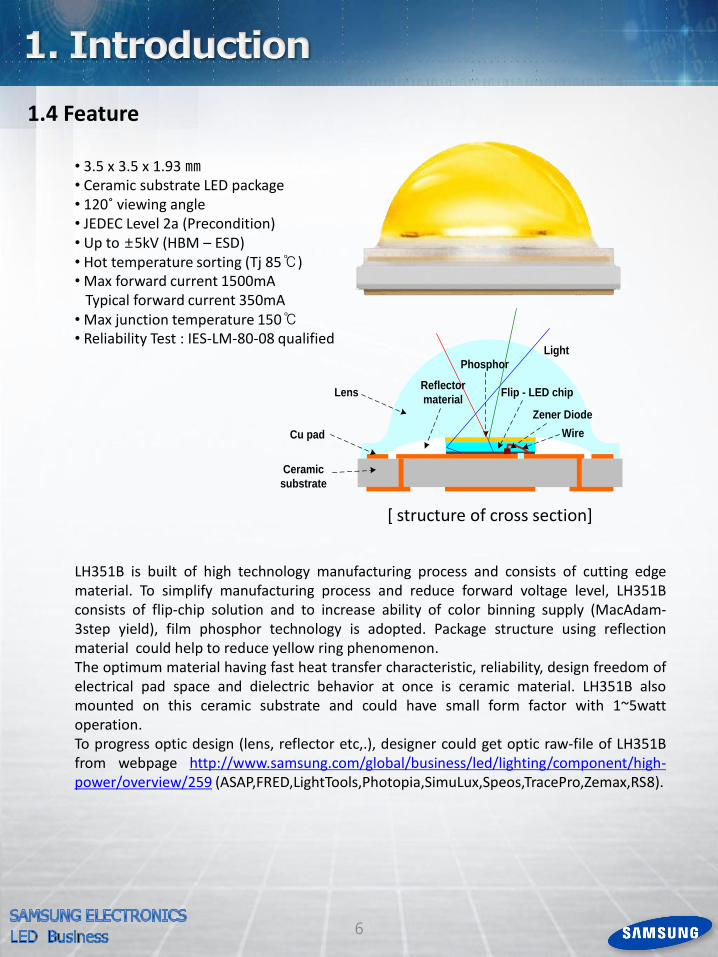
Ceramic
substrate
Cu pad
LensReflector
material
Phosphor
Flip - LED chip
Zener Diode
Wire
Light
• 3.5 x 3.5 x 1.93 ㎜ • Ceramic substrate LED package • 120˚ viewing angle • JEDEC Level 2a (Precondition) • Up to ±5kV (HBM – ESD) • Hot temperature sorting (Tj 85℃) • Max forward current 1500mA Typical forward current 350mA • Max junction temperature 150℃ • Reliability Test : IES-LM-80-08 qualified
LH351B is built of high technology manufacturing process and consists of cutting edge material. To simplify manufacturing process and reduce forward voltage level, LH351B consists of flip-chip solution and to increase ability of color binning supply (MacAdam-3step yield), film phosphor technology is adopted. Package structure using reflection material could help to reduce yellow ring phenomenon. The optimum material having fast heat transfer characteristic, reliability, design freedom of electrical pad space and dielectric behavior at once is ceramic material. LH351B also mounted on this ceramic substrate and could have small form factor with 1~5watt operation. To progress optic design (lens, reflector etc,.), designer could get optic raw-file of LH351B from webpage http://www.samsung.com/global/business/led/lighting/component/high-power/overview/259 (ASAP,FRED,LightTools,Photopia,SimuLux,Speos,TracePro,Zemax,RS8).
[ structure of cross section]
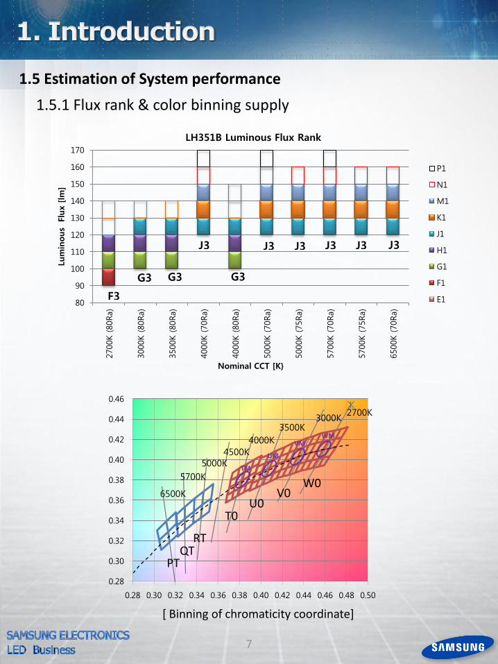
1.5 Estimation of System performance
7
1.5.1 Flux rank & color binning supply
2700K 3000K
3500K
4000K
4500K 5000K
5700K
6500K
0.28
0.30
0.32
0.34
0.36
0.38
0.40
0.42
0.44
0.46
0.28 0.30 0.32 0.34 0.36 0.38 0.40 0.42 0.44 0.46 0.48 0.50
[ Binning of chromaticity coordinate]
W0 V0
U0 T0
RT QT
PT
WM VM
UM
TM
80
90
100
110
120
130
140
150
160
170
2700K (80Ra)
3000K (80Ra)
3500K (80Ra)
4000K (70Ra)
4000K (80Ra)
5000K (70Ra)
5000K (75Ra)
5700K (70Ra)
5700K (75Ra)
6500K (70Ra)
Lum
inous
Flu
x [
lm]
Nominal CCT [K}
LH351B Luminous Flux Rank
P1
N1
M1
K1
J1
H1
G1
F1
E1 F3
G3 G3
J3 J3
G3
J3 J3 J3 J3
8
351Z PSU
efficiency Optic
efficiency current
[A] # of LEDs
Range Flux rank
Vf rank
lm W lm/W
Case1-1 Worst H1 max 917 16.7 54.8
(80%/80%) 80% 80% 0.6 7 Typical J1 typ 1000 16.2 61.8
Best K1 min 1083 15.1 71.8
Case1-2 Worst H1 max 974 15.8 61.8
(85%/85%) 85% 85% 0.6 7 Typical J1 typ 1063 15.2 69.8
Best K1 min 1151 14.2 81.1
Case1-3 Worst H1 max 1031 14.9 69.3
(90%/90%) 90% 90% 0.6 7 Typical J1 typ 1125 14.4 78.2
Best K1 min 1219 13.4 90.9
351Z PSU
efficiency Optic
efficiency Current
[A] # of LEDs
Range Flux rank
Vf rank
lm W lm/W
Case2-1 Worst H1 max 883 17 51.9
(80%/80%) 80% 80% 0.7 6 Typical J1 typ 964 16.5 58.6
Best K1 min 1044 15.3 73.5
Case2-2 Worst H1 max 939 16 58.6
(85%/85%) 85% 85% 0.7 6 Typical J1 typ 1024 15.5 66.1
Best K1 min 1109 144 76.8
Case2-3 Worst H1 max 994 15.1 65.7
(90%/90%) 90% 90% 0.7 6 Typical J1 typ 1084 14.6 74.1
Best K1 min 1174 13.6 86.2
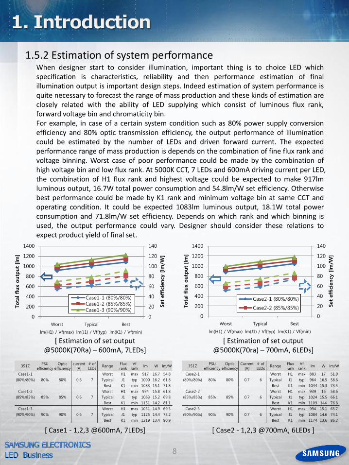
1.5.2 Estimation of system performance When designer start to consider illumination, important thing is to choice LED which specification is characteristics, reliability and then performance estimation of final illumination output is important design steps. Indeed estimation of system performance is quite necessary to forecast the range of mass production and these kinds of estimation are closely related with the ability of LED supplying which consist of luminous flux rank, forward voltage bin and chromaticity bin. For example, in case of a certain system condition such as 80% power supply conversion efficiency and 80% optic transmission efficiency, the output performance of illumination could be estimated by the number of LEDs and driven forward current. The expected performance range of mass production is depends on the combination of fine flux rank and voltage binning. Worst case of poor performance could be made by the combination of high voltage bin and low flux rank. At 5000K CCT, 7 LEDs and 600mA driving current per LED, the combination of H1 flux rank and highest voltage could be expected to make 917lm luminous output, 16.7W total power consumption and 54.8lm/W set efficiency. Otherwise best performance could be made by K1 rank and minimum voltage bin at same CCT and operating condition. It could be expected 1083lm luminous output, 18.1W total power consumption and 71.8lm/W set efficiency. Depends on which rank and which binning is used, the output performance could vary. Designer should consider these relations to expect product yield of final set.
0
20
40
60
80
100
120
140
0
200
400
600
800
1000
1200
1400
Worst
lm(H1) / Vf(max)
Typical
lm(J1) / Vf(typ)
Best
lm(K1) / Vf(min)
Set eff
icie
ncy
[lm
/W]
Tota
l flux o
utp
ut [lm
]
Case1-1 (80%/80%) Case1-2 (85%/85%) Case1-3 (90%/90%)
0
20
40
60
80
100
120
140
0
200
400
600
800
1000
1200
1400
Worst
lm(H1) / Vf(max)
Typical
lm(J1) / Vf(typ)
Best
lm(K1) / Vf(min) Set eff
icie
ncy
[lm
/W]
Tota
l flux o
utp
ut [lm
]
Case2-1 (80%/80%)
Case2-2 (85%/85%)
[ Case1 - 1,2,3 @600mA, 7LEDs] [ Case2 - 1,2,3 @700mA, 6LEDs ]
[ Estimation of set output @5000K(70Ra) – 600mA, 7LEDs]
[ Estimation of set output @5000K(70ra) – 700mA, 6LEDs]
9
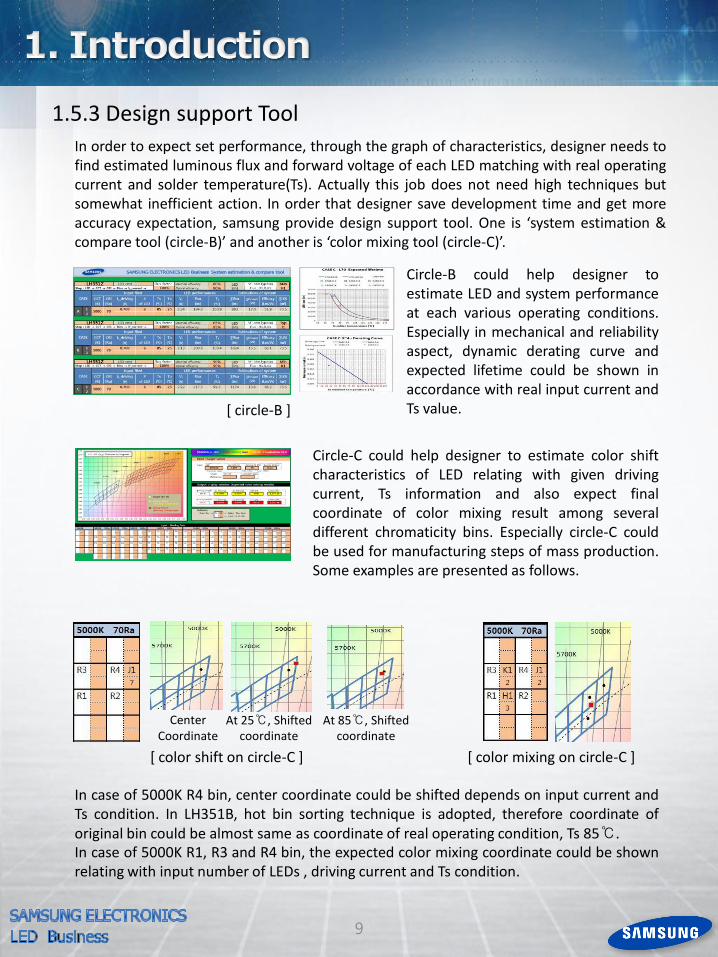
1.5.3 Design support Tool
In order to expect set performance, through the graph of characteristics, designer needs to find estimated luminous flux and forward voltage of each LED matching with real operating current and solder temperature(Ts). Actually this job does not need high techniques but somewhat inefficient action. In order that designer save development time and get more accuracy expectation, samsung provide design support tool. One is ‘system estimation & compare tool (circle-B)’ and another is ‘color mixing tool (circle-C)’.
Circle-B could help designer to estimate LED and system performance at each various operating conditions. Especially in mechanical and reliability aspect, dynamic derating curve and expected lifetime could be shown in accordance with real input current and Ts value. [ circle-B ]
Circle-C could help designer to estimate color shift characteristics of LED relating with given driving current, Ts information and also expect final coordinate of color mixing result among several different chromaticity bins. Especially circle-C could be used for manufacturing steps of mass production. Some examples are presented as follows.
In case of 5000K R4 bin, center coordinate could be shifted depends on input current and Ts condition. In LH351B, hot bin sorting technique is adopted, therefore coordinate of original bin could be almost same as coordinate of real operating condition, Ts 85℃. In case of 5000K R1, R3 and R4 bin, the expected color mixing coordinate could be shown relating with input number of LEDs , driving current and Ts condition.
[ color shift on circle-C ] [ color mixing on circle-C ]
Center Coordinate
At 25℃, Shifted coordinate
At 85℃, Shifted coordinate
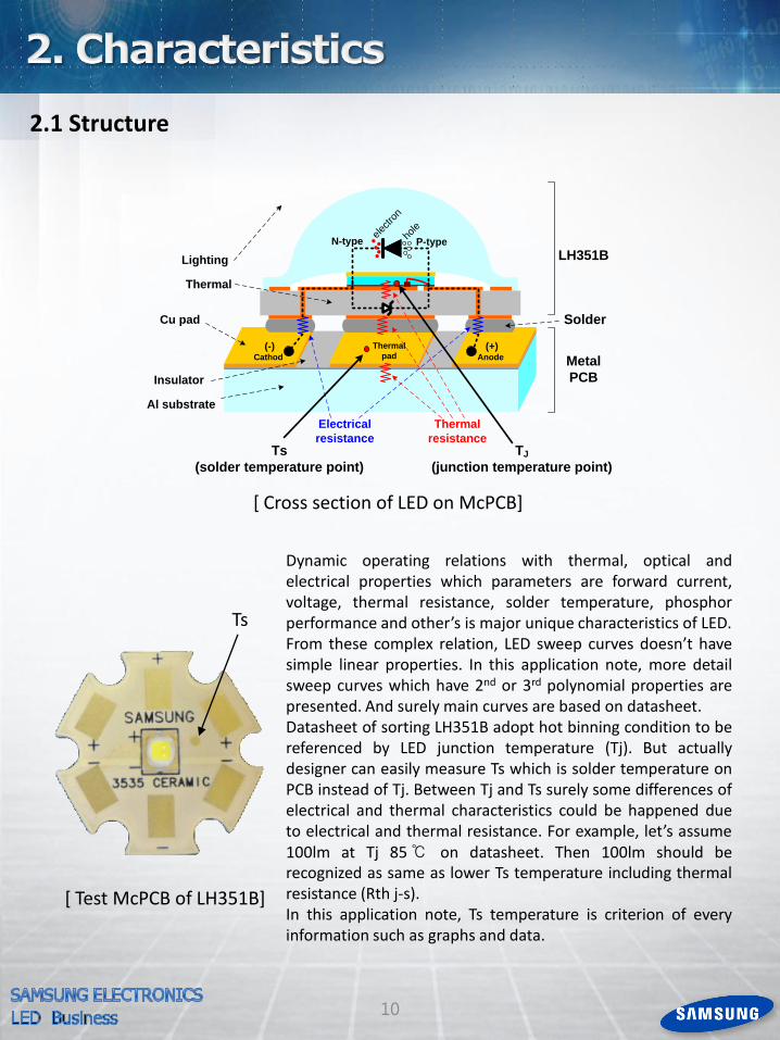
2.1 Structure
10
(-)Cathod
(+)Anode
P-typeN-type
Thermal
pad
Lighting
Thermal
Al substrate
Cu pad
Insulator
Metal
PCB
LH351B
Solder
Electrical
resistance
Thermal
resistanceTs
(solder temperature point)
TJ
(junction temperature point)
elec
tron
hole
[ Cross section of LED on McPCB]
Dynamic operating relations with thermal, optical and electrical properties which parameters are forward current, voltage, thermal resistance, solder temperature, phosphor performance and other’s is major unique characteristics of LED. From these complex relation, LED sweep curves doesn’t have simple linear properties. In this application note, more detail sweep curves which have 2nd or 3rd polynomial properties are presented. And surely main curves are based on datasheet. Datasheet of sorting LH351B adopt hot binning condition to be referenced by LED junction temperature (Tj). But actually designer can easily measure Ts which is solder temperature on PCB instead of Tj. Between Tj and Ts surely some differences of electrical and thermal characteristics could be happened due to electrical and thermal resistance. For example, let’s assume 100lm at Tj 85℃ on datasheet. Then 100lm should be recognized as same as lower Ts temperature including thermal resistance (Rth j-s). In this application note, Ts temperature is criterion of every information such as graphs and data.
[ Test McPCB of LH351B]
Ts
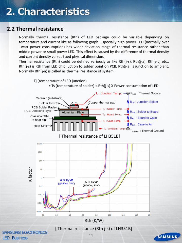
2.2 Thermal resistance
11
4.0 K/W (@350㎃, 25℃) 6.0 K/W
(@700㎃, 85℃)
Normally thermal resistance (Rth) of LED package could be variable depending on temperature and current like as following graph. Especially high power LED (normally over 1watt power consumption) has wider deviation range of thermal resistance rather than middle power or small power LED. This effect is caused by the difference of thermal density and current density versus fixed physical dimension. Thermal resistance (Rth) could be defined variously as like Rth(j-s), Rth(j-a), Rth(s-c) etc,. Rth(j-s) is Rth from LED chip juction to solder point on PCB, Rth(j-a) is junction to ambient. Normally Rth(j-a) is called as thermal resistance of system. Tj (temperature of LED junction) = Ts (temperature of solder) + Rth(j-s) X Power consumption of LED
[ Thermal resistance (Rth j-s) of LH351B]
Copper thermal pad RJS : Junction-Solder
RBC : Board to Case
RSB : Solder to Board
RCA : Case to Air
PLED : Thermal Source
TS : Solder Temp.
TJ : Junction Temp.
TB : Board Temp.
TC : Case Temp.
TA : Ambient Temp.
Aluminium Plate
Classical TIM
to heat-sink
Heat Sink
PCB Dielectric layerPCB Solder Pads
Ceramic (substrate)
Solder to PCB
Tambient : Thermal Ground
[ Thermal resistance of LH351B]
Rth (K/W)
K fa
cto
r
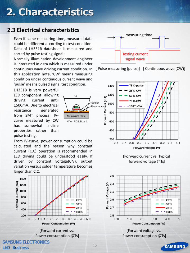
2.3 Electrical characteristics
12
Even if same measuring time, measured data could be different according to test condition. Data of LH351B datasheet is measured and sorted by pulse testing signal. Normally illumination development engineer is interested in data which is measured under continuous wave driving current condition. In this application note, ‘CW’ means measuring condition under continuous current wave and ‘pulse’ means pulsed signal test condition.
[ Pulse measuring (pulse)] [ Continuous wave (CW)]
measuring time
Testing current signal wave
Aluminium Plate
Solder
Vf
Resistance
Vf on PCB Board
LH351B is very powerful LED component allowing driving current until 1500mA. Due to electrical resistance generated from SMT process, IV-curve measured by CW has somewhat incline properties rather than pulse testing.
From IV-curve, power consumption could be calculated and the reason why constant current (C.C) operation is recommended in LED driving could be understood easily. If driven by constant voltage(C.V), output variation versus solder temperature becomes larger than C.C.
[Forward current vs. Typical forward voltage @Ts]
[Forward current vs. Power consumption @Ts]
[Forward voltage vs. Power consumption @Ts]
200
400
600
800
1000
1200
1400
2.6 2.7 2.8 2.9 3.0 3.1 3.2 3.3 3.4
Fo
rward
Cu
rren
t (m
A)
Forward Voltage (V)
78℃-pulse
25℃-CW
50℃-CW
78℃-CW
100℃-CW
200
400
600
800
1000
1200
1400
0.0 0.5 1.0 1.5 2.0 2.5 3.0 3.5 4.0 4.5 5.0
Fo
rward
Cu
rren
t (m
A)
Power Consumption (W)
25℃
50℃
78℃
100℃
2.5
2.7
2.9
3.1
3.3
3.5
0.0 1.0 2.0 3.0 4.0 5.0
Fo
rward
Vo
ltag
e (
V)
Power Consumption (W)
25℃
50℃
78℃
100℃
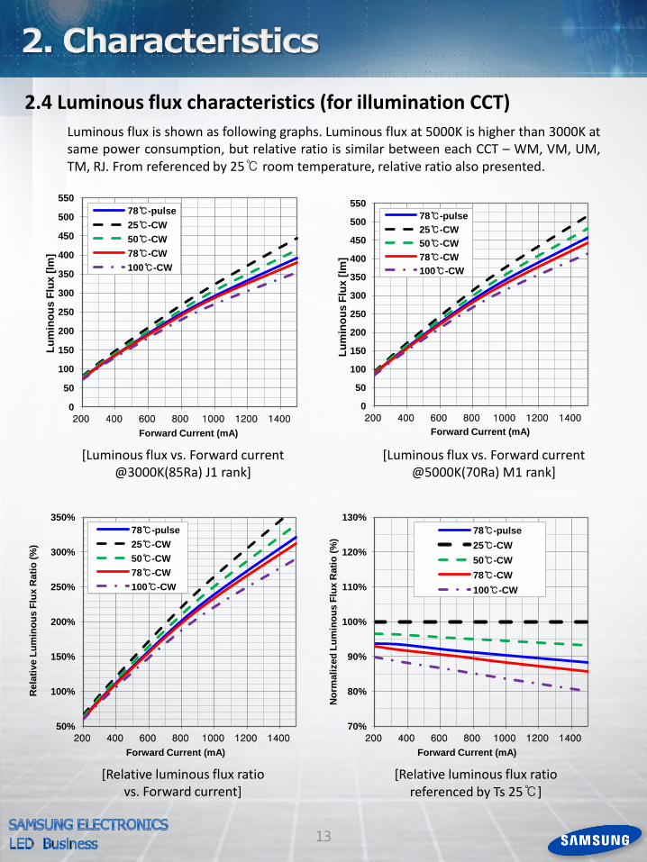
2.4 Luminous flux characteristics (for illumination CCT)
13
Luminous flux is shown as following graphs. Luminous flux at 5000K is higher than 3000K at same power consumption, but relative ratio is similar between each CCT – WM, VM, UM, TM, RJ. From referenced by 25℃ room temperature, relative ratio also presented.
[Luminous flux vs. Forward current @3000K(85Ra) J1 rank]
[Luminous flux vs. Forward current @5000K(70Ra) M1 rank]
[Relative luminous flux ratio vs. Forward current]
[Relative luminous flux ratio referenced by Ts 25℃]
0
50
100
150
200
250
300
350
400
450
500
550
200 400 600 800 1000 1200 1400
Lu
min
ou
s F
lux
[lm
]
Forward Current (mA)
78℃-pulse
25℃-CW
50℃-CW
78℃-CW
100℃-CW
0
50
100
150
200
250
300
350
400
450
500
550
200 400 600 800 1000 1200 1400
Lu
min
ou
s F
lux
[lm
]
Forward Current (mA)
78℃-pulse
25℃-CW
50℃-CW
78℃-CW
100℃-CW
50%
100%
150%
200%
250%
300%
350%
200 400 600 800 1000 1200 1400
Rela
tive L
um
ino
us
Flu
x R
ati
o (
%)
Forward Current (mA)
78℃-pulse
25℃-CW
50℃-CW
78℃-CW
100℃-CW
70%
80%
90%
100%
110%
120%
130%
200 400 600 800 1000 1200 1400
No
rmali
zed
Lu
min
ou
s F
lux
Rati
o (
%)
Forward Current (mA)
78℃-pulse
25℃-CW
50℃-CW
78℃-CW
100℃-CW
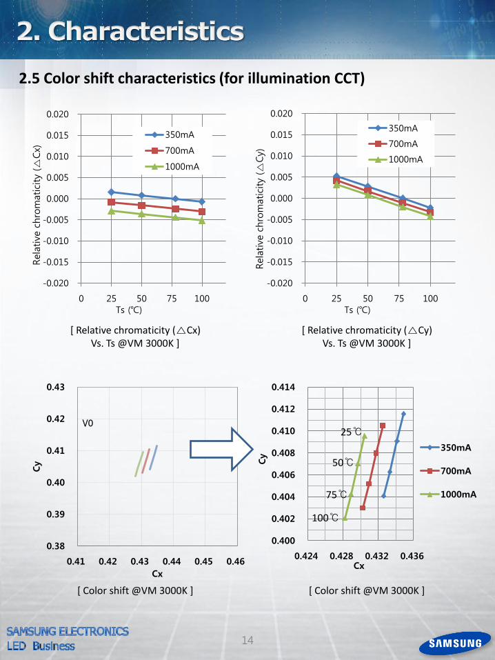
2.5 Color shift characteristics (for illumination CCT)
14
0.400
0.402
0.404
0.406
0.408
0.410
0.412
0.414
0.424 0.428 0.432 0.436
Cy
Cx
350mA
700mA
1000mA
0.38
0.39
0.40
0.41
0.42
0.43
0.41 0.42 0.43 0.44 0.45 0.46
Cy
Cx
V0
-0.020
-0.015
-0.010
-0.005
0.000
0.005
0.010
0.015
0.020
0 25 50 75 100
Rela
tive
chro
matici
ty (△
Cx)
Ts (℃)
350mA
700mA
1000mA
-0.020
-0.015
-0.010
-0.005
0.000
0.005
0.010
0.015
0.020
0 25 50 75 100
Rela
tive
chro
matici
ty (△
Cy)
Ts (℃)
350mA
700mA
1000mA
[ Relative chromaticity (△Cy) Vs. Ts @VM 3000K ]
[ Relative chromaticity (△Cx) Vs. Ts @VM 3000K ]
[ Color shift @VM 3000K ] [ Color shift @VM 3000K ]
25℃
50℃
75℃
100℃
2.5 Color shift characteristics (for illumination CCT)
15
-0.020
-0.015
-0.010
-0.005
0.000
0.005
0.010
0.015
0.020
0 25 50 75 100
Rela
tive
chro
matici
ty (△
Cx)
Ts (℃)
350mA
700mA
1000mA
-0.020
-0.015
-0.010
-0.005
0.000
0.005
0.010
0.015
0.020
0 25 50 75 100
Rela
tive
chro
matici
ty (△
Cy)
Ts (℃)
350mA
700mA
1000mA
0.350
0.352
0.354
0.356
0.358
0.360
0.362
0.340 0.344 0.348 0.352
Cy
Cx
350mA
700mA
1000mA
0.33
0.34
0.35
0.36
0.37
0.38
0.33 0.34 0.35 0.36
Cy
Cx
RJ
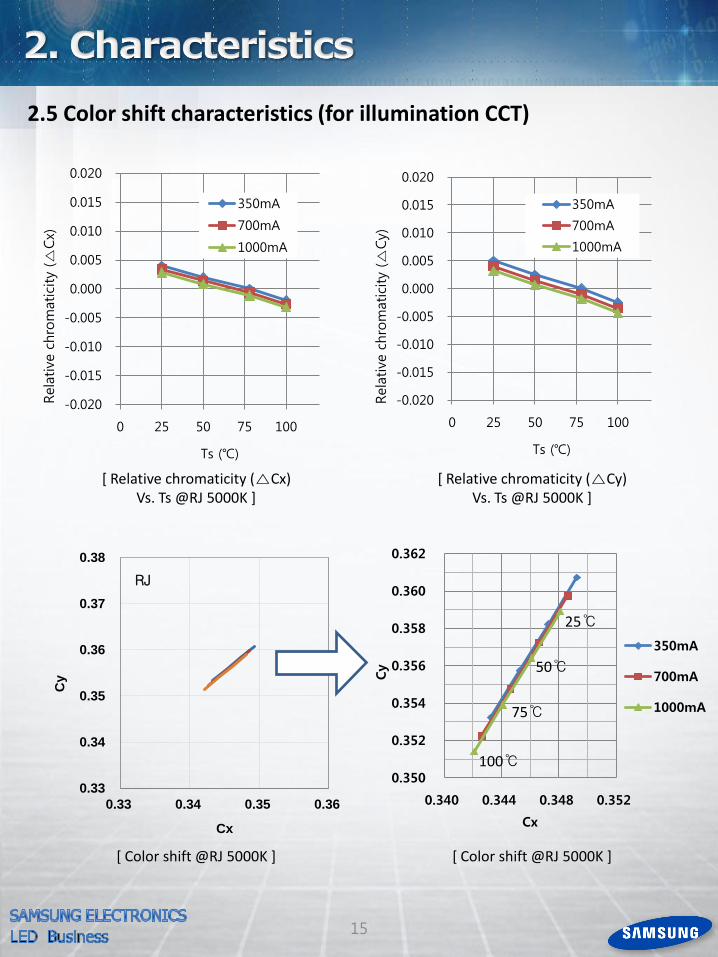
[ Relative chromaticity (△Cy) Vs. Ts @RJ 5000K ]
[ Relative chromaticity (△Cx) Vs. Ts @RJ 5000K ]
[ Color shift @RJ 5000K ] [ Color shift @RJ 5000K ]
25℃
50℃
75℃
100℃
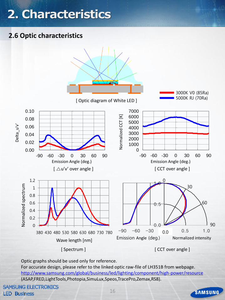
2.6 Optic characteristics
16
-90 -60 -30 0 0.0
0.5
1.0
0.0 0.5 1.0
60
30
0
0.0
90
0.00
0.02
0.04
0.06
0.08
0.10
-90 -60 -30 0 30 60 90
Del
ta_
u'v
'
Emission Angle (deg.)
0
1000
2000
3000
4000
5000
6000
7000
-90 -60 -30 0 30 60 90
No
rmal
ized
CC
T [K
]
Emission Angle (deg.)
3000K V0 (85Ra) 5000K RJ (70Ra)
Emission Angle (deg.) Normalized intensity
0
0.2
0.4
0.6
0.8
1
1.2
380 430 480 530 580 630 680 730 780
No
rmal
ized
sp
ectr
um
Wave length [nm]
[ Optic diagram of White LED ]
Optic graphs should be used only for reference. For accurate design, please refer to the linked optic raw-file of LH351B from webpage. http://www.samsung.com/global/business/led/lighting/component/high-power/resource (ASAP,FRED,LightTools,Photopia,SimuLux,Speos,TracePro,Zemax,RS8).
[ △u’v’ over angle ] [ CCT over angle ]
[ Spectrum ] [ CCT over angle ]
400
800
1200
1600
2000
2400
0 0.2 0.4 0.6 0.8 1 1.2
Lum
inous
flux
outp
ut [lm
]
Forward current [A]
measurement
simulation
3.1 Current sweep comparison
17
80%
120%
160%
200%
240%
0 0.2 0.4 0.6 0.8 1 1.2
Rel
ativ
e lu
min
ou
s fl
ux
rati
o [
%]
Forward current [A]
ratio_measurement
ratio_simulation
For verification of Tool (circle-B) and for testing LH351B, simple experiment is done. Without 2nd optic and power supply unit(PSU), the current sweep performance of assembled module mounting LH351B - 6 LEDs, McPCB and heat-sink are measured and then compared with data from Tool at 25℃ Ts condition.
[ Real module test without 2nd optic and PSU ]
[ Current sweep simulation ]
[ Luminous flux compare @25℃ measurement vs simulation ]
[ Relative luminous flux ratio compare @25℃ measurement vs simulation ]
From the graph of measurement and simulation, two points come to be noticeable. One is that their absolute real data does not equal with each case, another is their deviation ratio is almost same. In case of simulation, deviation parameter is linked with initial starting value which is same value of datasheet. Otherwise, measurement value might need some calibration due to wrong center allocation of DUT(device under test) with integrating sphere and also need to check calibration file of software. Through this simple test, deviation used in Tool might be considered as a quite reliable. And in order to get more exact measuring data, considerable calibration of measuring instrument would be necessary when real measurement.
958lm
868lm
LH351B LED cost Flux factor Electrical efficiency 100~40
% 100% LED Vf : Min.Typ.Max Typ
Sorting IF_driving =
0.350 A Tj_max. = 150 ℃
Step : LED → CCT → CRI → Bins → IF_current → 100% Optical efficiency 100~40
% 100% Bins Flux : J1,K1,M1,N1 M1
Sorting Temperature
= 85 ℃ IF_max. = 1.500 A
CASE
Input filed LED performances @min/flux_rank Estimations of system Derating performance
CCT [K]
CRI [Ra]
IF_driving [A]
# of LED
Ts [℃]
Ta [℃]
VF
[V] Flux [㏐]
$ /100lm
TJ
[℃] ∑Flux [㏐]
∑Power [W]
Efficacy
[Lm/W]
∑LES [㎟]
∑cost [$]
Rth(J-a) (℃/W)
IF_max. (A)
IF_margin (A)
Location
A
1
5000 70
0.350 6 25 25 2.86 159.7 29.0 958 6.0 159.4 74 4.0 1.500 1.150 Safe zone
2 0.500 6 25 25 2.92 217.5 30.8 1305 8.8 148.7 74 4.0 1.500 1.000 Safe zone
3 0.700 6 25 25 2.99 289.4 33.4 1736 12.6 138.1 74 4.0 1.500 0.800 Safe zone
4 1.000 6 25 25 3.07 386.2 37.3 2317 18.4 125.9 74 4.0 1.500 0.500 Safe zone
5
6
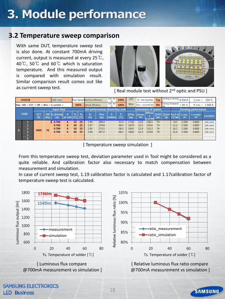
3.2 Temperature sweep comparison
18
600
800
1000
1200
1400
1600
1800
0 20 40 60 80
Lum
ino
us
flu
x o
utp
ut
[lm
]
Ts. Temperature of solder [℃]
measurement
simulation
80%
85%
90%
95%
100%
105%
0 20 40 60 80
Rel
ativ
e lu
min
ou
s fl
ux
rati
o [
%]
Ts. Temperature of solder [℃]
ratio_measurement
ratio_simulation
With same DUT, temperature sweep test is also done. At constant 700mA driving current, output is measured at every 25℃, 40℃, 50℃ and 60℃ which is saturation temperature. And this measured output is compared with simulation result. Similar comparison result comes out like as current sweep test.
[ Real module test without 2nd optic and PSU ]
[ Temperature sweep simulation ]
[ Luminous flux compare @700mA measurement vs simulation ]
[ Relative luminous flux ratio compare @700mA measurement vs simulation ]
From this temperature sweep test, deviation parameter used in Tool might be considered as a quite reliable. And calibration factor also necessary to match compensation between measurement and simulation. In case of current sweep test, 1.19 calibration factor is calculated and 1.17calibration factor of temperature sweep test is calculated.
1736lm
1549lm
LH351B LED cost Flux factor Electrical efficiency 100~40
% 100% LED Vf : Min.Typ.Max Typ
Sorting IF_driving =
0.350 A Tj_max. = 150 ℃
Step : LED → CCT → CRI → Bins → IF_current → 100% Optical efficiency 100~40
% 100% Bins Flux : J1,K1,M1,N1 M1
Sorting Temperature
= 85 ℃ IF_max. = 1.500 A
CASE
Input filed LED performances @min/flux_rank Estimations of system Derating performance
CCT [K]
CRI [Ra]
IF_driving [A]
# of LED
Ts [℃]
Ta [℃]
VF
[V] Flux [㏐]
$ /100lm
TJ
[℃] ∑Flux [㏐]
∑Power [W]
Efficacy
[Lm/W]
∑LES [㎟]
∑cost [$]
Rth(J-a) (℃/W)
IF_max. (A)
IF_margin (A)
Location
A
1
5000 70
0.700 6 25 25 2.99 289.4 33.4 1736 12.6 138.1 74 4.0 1.500 0.800 Safe zone
2 0.700 6 40 25 2.97 279.8 48.3 1679 12.5 134.6 74 11.2 1.500 0.800 Safe zone
3 0.700 6 50 25 2.95 273.5 58.3 1641 12.4 132.2 74 16.1 1.500 0.800 Safe zone
4 0.700 6 60 25 2.94 267.2 68.2 1603 12.3 129.8 74 21.0 1.500 0.800 Safe zone
5
6
3.3 Derating curve
19
0.000
0.200
0.400
0.600
0.800
1.000
1.200
0 20 40 60 80 100 120 140 M
axim
um
cu
rren
t [A
]
Ta Ambient temperature [℃]
CASE-C.1
CASE-C.1
0.000
0.200
0.400
0.600
0.800
1.000
1.200
0 20 40 60 80 100 120 140
Max
imu
m c
urr
ent
[A]
Ta Ambient temperature [℃]
CASE-C.1 CASE-C.2
CASE-C.1 CASE-C.2
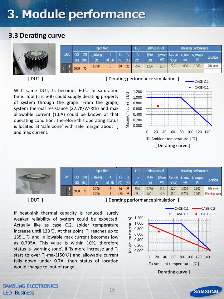
With same DUT, Ts becomes 60℃ in saturation time. Tool (circle-B) could supply derating property of system through the graph. From the graph, system thermal resistance (22.7K/W-Rth) and max allowable current (1.0A) could be known at that operating condition. Therefore this operating status is located at ‘safe zone’ with safe margin about Tj and max current.
[ Derating performance simulation ]
[ Derating performance simulation ]
[ Derating curve ]
[ Derating curve ]
[ DUT ]
[ DUT ]
If heat-sink thermal capacity is reduced, surely weaker reliability of system could be expected. Actually like as case C.2, solder temperature increase until 120℃. At that point, Tj reaches up to 135.1℃ and allowable max current becomes low as 0.795A. This value is within 10%, therefore status is ‘warning zone’. If Ts more increase and Tj start to over Tj-max(150℃) and allowable current falls down under 0.7A, then status of location would change to ‘out of range’.
Solder Mask
O X (miss- align)
X (solder-lack)
X (solder-incline)
X (thick-solder)
Pick &
Place
O X (fault-cathode)
X (fault-cathode)
X (miss-place)
After reflow
O X (solder-
lack) X (solder-
ball)
4.1 SMT guide
20
[ The nozzle of pick-up & place tool ]
Unit : mm
Vac. Hole Ø 1
1.2
3
1.0
9
120˚
Ø 3.1
Ø 4.0
[ Recommended foot-print for SMT ]
Ø 3.1
Ø 4.0
[ Recommended example ]
Date Revision History Writer
Drawn Approved
2014.7.4 -. New Version Y. J. Lee I.H. Choi
21