Embed Size (px)
Citation preview

1
www.fairchildsemi.com
1
Board Level Evaluation of Power Quad
Flat No-Lead (PQFN) Packages
Marlon Bartolo and Erwin Almagro
2
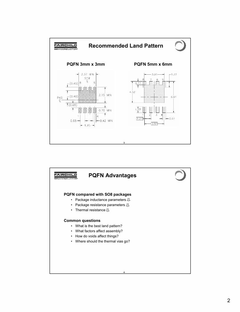
PQFN 3mm x 3mm
PQFN 5mm x 6mm
PQFN Packages
2
3
PQFN 3mm x 3mm PQFN 5mm x 6mm
Recommended Land Pattern
4
PQFN Advantages
PQFN compared with SO8 packages
• Package inductance parameters
• Package resistance parameters
• Thermal resistance
Common questions
• What is the best land pattern?
• What factors affect assembly?
• How do voids affect things?
• Where should the thermal vias go?
3
5
Presentation Outline
• Introduction
• PQFN 5x6 and PQFN 3x3 Package Assembly and Structure
• Experimentation and Discussion
• Solder Paste Printing and Stencil Design
• Different Paste Evaluations
• Component Placement
• Reflow Process
• Board Level Stress Tests
• Thermal Resistance Measurement and Board Design
• Effect of Thermal Via-in-Pad
• Summary
6
Introduction
• Typical board assembly processes are crucial to
achieving a good board assembly
• For PQFN packages, stencil aperture design is critical
• Solder paste from different manufacturers are studied
and evaluated for which aperture designs the paste suits
• Placement of the component on the board with printed
solder pastes can be critical
• Discussions about thermal resistance performance
4
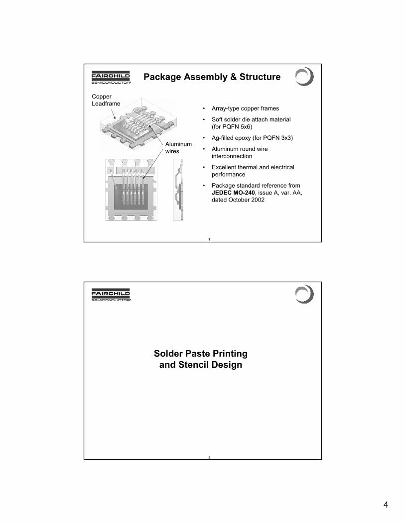
7
Package Assembly & Structure
• Array-type copper frames
• Soft solder die attach material
(for PQFN 5x6)
• Ag-filled epoxy (for PQFN 3x3)
• Aluminum round wire
interconnection
• Excellent thermal and electrical
performance
• Package standard reference from
JEDEC MO-240, issue A, var. AA,
dated October 2002
Copper
Leadframe
Aluminum
wires
8
Solder Paste Printing
and Stencil Design
5
9
Defects in Board Assembly
• Generally attributed to printing process and stencil design
• Common defects in PQFN
• Solder beading
• Bridging
• Open lead connection (package tilting)
• Inconsistent paste volume
• These are due to excessive solder on board pad for the
exposed die pad (drain connection)
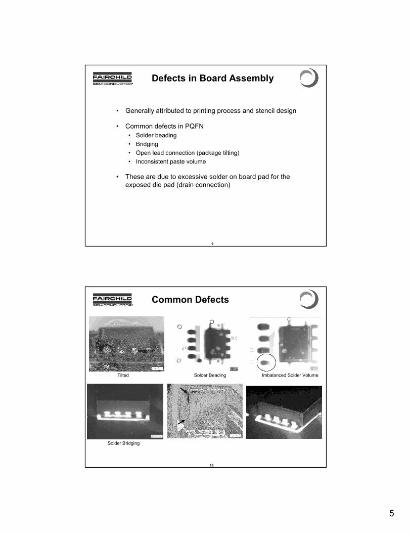
10
Common Defects
Tilted
Solder Bridging
Solder Beading Imbalanced Solder Volume
6
11
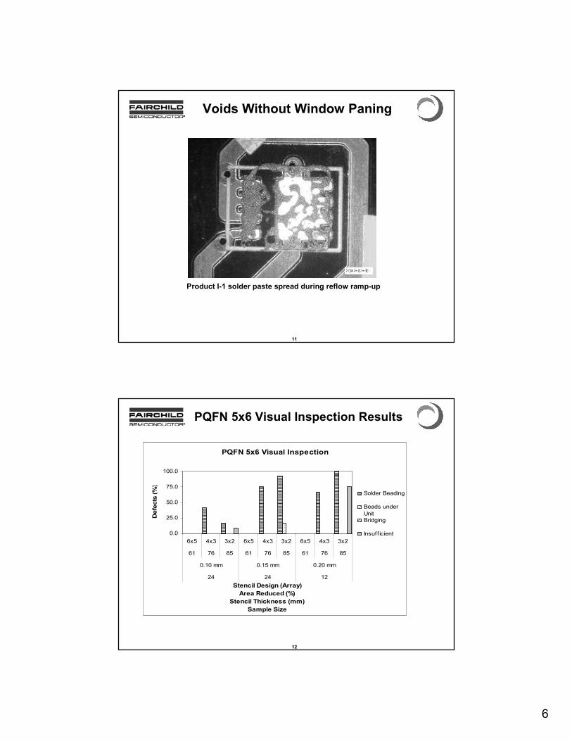
Product I-1 solder paste spread during reflow ramp-up
Voids Without Window Paning
12
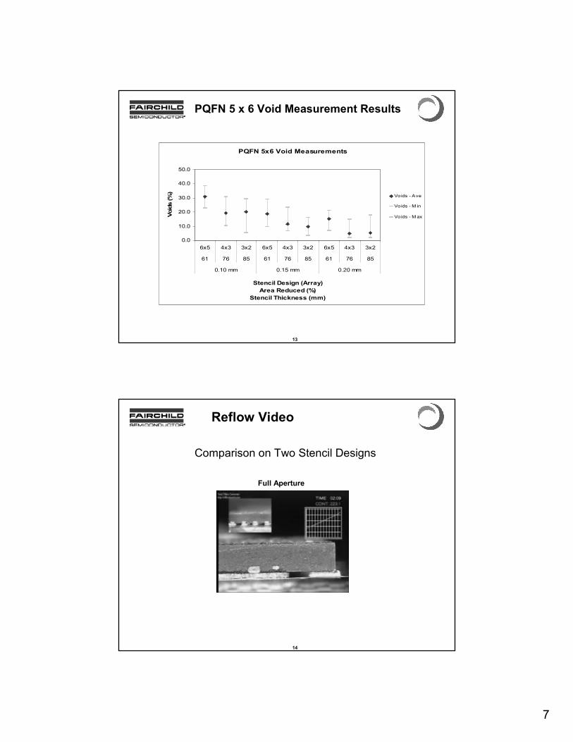
PQFN 5x6 Visual Inspection Results
PQFN 5x6 Visual Inspection
0.0
25.0
50.0
75.0
100.0
6x5 4x3 3x2 6x5 4x3 3x2 6x5 4x3 3x2
61 76 85 61 76 85 61 76 85
0.10 mm 0.15 mm 0.20 mm
24 24 12
Stencil Design (Array)
Area Reduced (%)
Stencil Thickness (mm)
Sample Size
Defects (%)
Solder Beading
Beads under
Unit
Bridging
Insuff icient
7
13
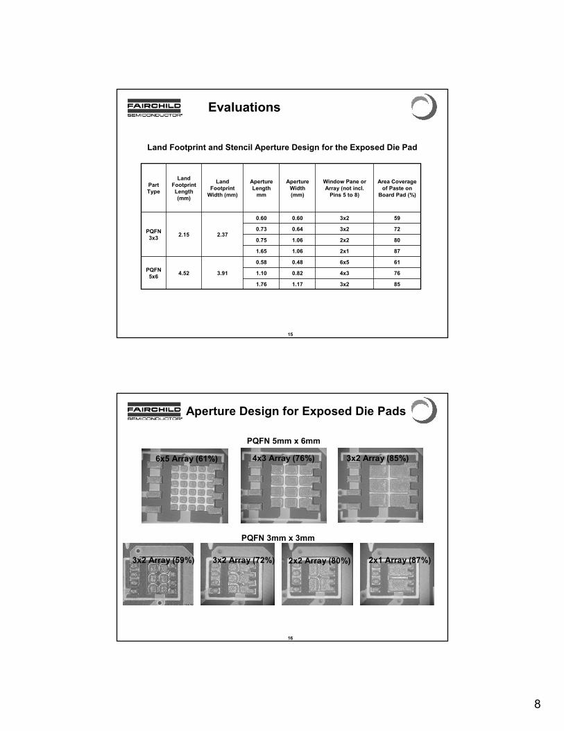
PQFN 5 x 6 Void Measurement Results
PQFN 5x6 Void Measurements
0.0
10.0
20.0
30.0
40.0
50.0
6x5 4x3 3x2 6x5 4x3 3x2 6x5 4x3 3x2
61 76 85 61 76 85 61 76 85
0.10 mm 0.15 mm 0.20 mm
Stencil Design (Array)
Area Reduced (%)
Stencil Thickness (mm)
Voids (%)
Voids - Ave
Voids - M in
Voids - Max
14
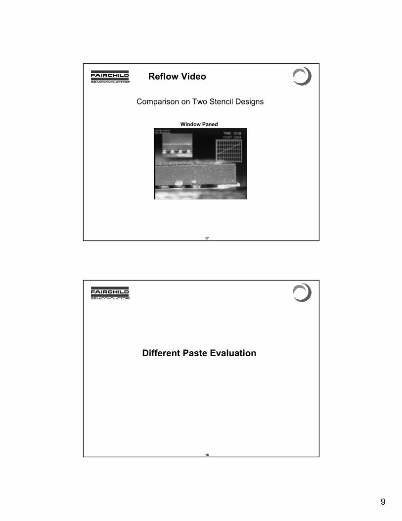
Reflow Video
Full Aperture
Comparison on Two Stencil Designs
8
15
Evaluations
Land Footprint and Stencil Aperture Design for the Exposed Die Pad
853x21.171.76
764x30.821.10
616x50.480.58
3.914.52PQFN
5x6
872x11.061.65
802x21.060.75
723x20.640.73
593x20.600.60
2.372.15PQFN
3x3
Area Coverage
of Paste on
Board Pad (%)
Window Pane or
Array (not incl.
Pins 5 to 8)
Aperture
Width
(mm)
Aperture
Length
mm
Land
Footprint
Width (mm)
Land
Footprint
Length
(mm)
Part
Type
16
Aperture Design for Exposed Die Pads
6x5 Array (61%) 4x3 Array (76%) 3x2 Array (85%)
3x2 Array (59%) 3x2 Array (72%) 2x2 Array (80%) 2x1 Array (87%)
PQFN 5mm x 6mm
PQFN 3mm x 3mm
9
17
Reflow Video
Window Paned
Comparison on Two Stencil Designs
18
Different Paste Evaluation

10
19
Matrix of Solder Paste Evaluation
SAC387 alloy, Type 3, ROL0Product E-1
SAC387 alloy, Type 3, ROL0Product H1
SAC387 alloy, Type 3, ROL0Product K-1
Sn63Pb37 alloy, Type 3, ROL0Product I-3
SAC387 alloy, Type 3, ROL0Product I-2
SAC387 alloy, Type 3, ROL0Product I-1
Paste DescriptionProduct Code
Different solder pastes evaluated in PQFN 5x6
20
Solder Paste Evaluation
• The three aperture designs and the stencil thickness of
0.15mm and 0.2mm were used in this evaluation
• Result showed better performance than the I-1
• Solder beading observed on H-1 using the 4x3 array stencil
aperture design (BUT, lower than the I-1)
• No defects are observed on the K-1 and E-1 solder pastes
• No defects on I-2 and I-3 solder pastes
• Void level is highest for the I-2 paste
• Other pastes are comparable with I-1 in terms of void
performance

11
21
Component Placement
22
Component Placement
Not compressed Offset PQFN 5x6 before
Compressed Offset PQFN 5x6 after reflow
12
23
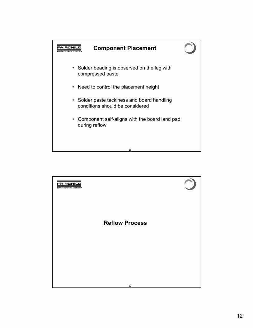
Component Placement
• Solder beading is observed on the leg with
compressed paste
• Need to control the placement height
• Solder paste tackiness and board handling
conditions should be considered
• Component self-aligns with the board land pad
during reflow
24
Reflow Process
13
25
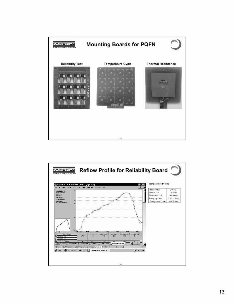
Mounting Boards for PQFN
Reliability Test Temperature Cycle Thermal Resistance
26
Reflow Profile for Reliability Board
Temperature Profile
Peak Temp 245 °C
Time >217 81 sec
Time 190-210 51.5 sec
Ramp up rate 0.50 °C/sec
Ramp down rate < 6 °C/sec
14
27
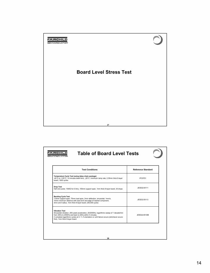
Board Level Stress Test
28
Table of Board Level Tests
JESD22-B103B
Vibration Test
Sinusoidal vibration, 20G peak acceleration, 20/2000Hz, logarithmic sweep of 1 decade/min
from 20Hz to 2000Hz and back to 20Hz within 4 minutes,
4 complete logarithmic cycles at X, Y, Z orientation or until failure occurs (whichever occurs
first), 1mm thick 8-layer board
JESD22-B113
Bending Cycle Test
110mm support span, 75mm load span, 2mm deflection, sinusoidal, 1mm/s,
10mm minimum distance with load anvil and edge of nearest component,
3mm anvil radius, 1mm thick 8-layer board, 200,000 cycles
JESD22-B111Drop Test
Half sine pulse; 1500G for 0.5ms, 105mm support span, 1mm thick 8-layer board, 30 drops
IPC9701
Temperature Cycle Test (using daisy chain package)
-40°C to +125°C, 10 minutes dwell time, ≤20°C / minimum ramp rate, 2.35mm thick 8-layer
board, 1000 cycles
Reference StandardTest Conditions

15
29
Cross-Sections of PQFN 3x3
Temperature cycle test
(-40 / 125°C test condition)
Bending cycle test
Drop test
Gate Lead (Pin#4) After Stress Test
30
Thermal Resistance Measurement
and Board Design
16
31
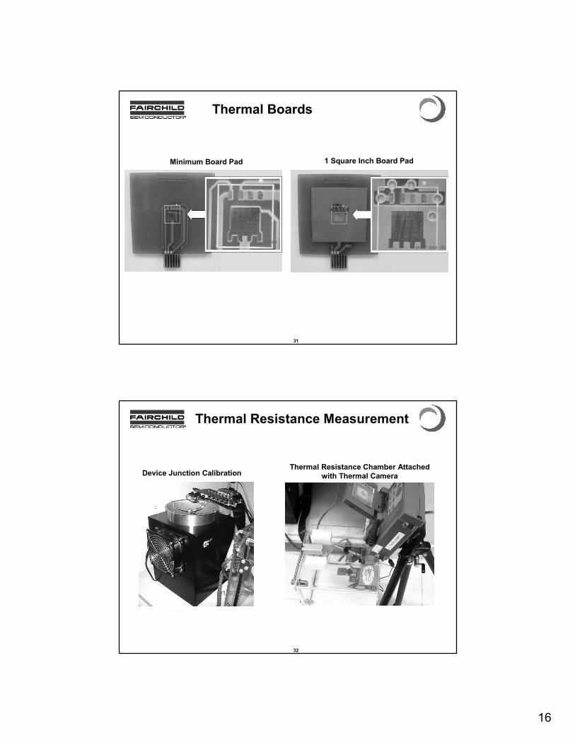
Thermal Boards
1 Square Inch Board PadMinimum Board Pad
32
Thermal Resistance Measurement
Thermal Resistance Chamber Attached
with Thermal CameraDevice Junction Calibration
17
33
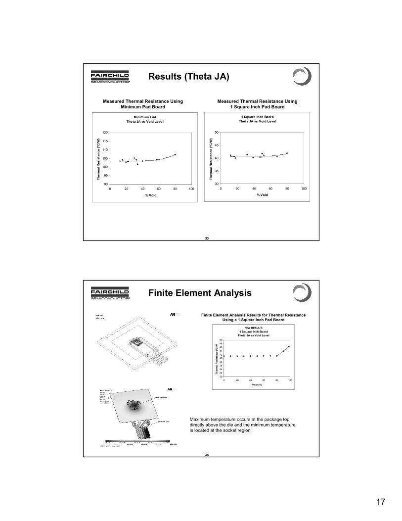
Results (Theta JA)
1 Square Inch Board
Theta JA vs Void Level
30
35
40
45
50
0 20 40 60 80 100
% Void
Therm
al Resistance (°C/W
)
Measured Thermal Resistance Using
Minimum Pad Board
Minimum Pad
Theta JA vs Void Level
90
95
100
105
110
115
120
0 20 40 60 80 100
% Void
Therm
al Resistance (°C/W
)Measured Thermal Resistance Using
1 Square Inch Pad Board
34
Finite Element Analysis
Maximum temperature occurs at the package top
directly above the die and the minimum temperature
is located at the socket region.
FEA RESULT:
1 Square Inch Board
Theta JA vs Void Level
30
32
34
36
38
40
42
44
46
48
50
0 20 40 60 80 100
Void (%)
Therm
al Resistance (ºC/W
)
Finite Element Analysis Results for Thermal Resistance
Using a 1 Square Inch Pad Board
18
35
Effect of Thermal Vias-in-Pad in the
Thermal Resistance Performance
of the PQFN Package
36
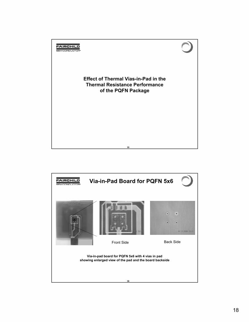
Via-in-pad board for PQFN 5x6 with 4 vias in pad
showing enlarged view of the pad and the board backside
Front Side Back Side
Via-in-Pad Board for PQFN 5x6
19
37
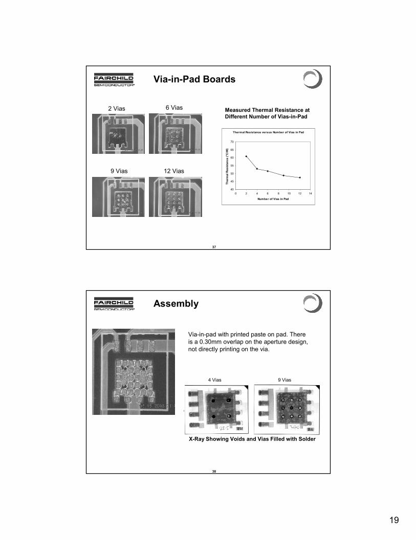
Via-in-Pad Boards
Thermal Resistance versus Number of Vias in Pad
40
45
50
55
60
65
70
0 2 4 6 8 10 12 14
Number of Vias in Pad
Therm
al Resistance (°C/W
)
Measured Thermal Resistance at
Different Number of Vias-in-Pad
2 Vias 6 Vias
9 Vias 12 Vias
38
Assembly
Via-in-pad with printed paste on pad. There
is a 0.30mm overlap on the aperture design,
not directly printing on the via.
X-Ray Showing Voids and Vias Filled with Solder
4 Vias 9 Vias
20
39
Summary
1. Stencil aperture design
• Reduction in stencil aperture size for the exposed
die pad is recommended
• Window paning the aperture for the exposed die
pad is recommended
2. Component placement
• Controlling the placement height is necessary
• X and Y placement should be limited to
0.20mm for the PQFN 5 mm x 6mm and
0.16mm for the PQFN 3mm x 3mm
40
Summary
3. Reflow conditions
• It is critical to control the temperature to which
the PQFN packages are exposed
• Different boards respond differently to same
reflow parameters
4. Board level stress test
• PQFN has passed the standards set by Fairchild
and the industry
• Wetting on the side wall of the sawn terminations
is not necessary

21
41
Summary
5. Effect of solder voids on the exposed die pad of
the package to thermal resistance
• Void does not significantly impact the thermal
resistance of the package (steady-state)
• Solder joint reliability should not be a concern on
the exposed die pad of the component
6. Thermal vias-in-pad
• Recommended to have thermal vias in pad
• In the use of through-hole vias, voiding should not
be a concern