Embed Size (px)
Citation preview

May 2017 Rev 0.3 1 / 72
Boya Microelectronics
Memory Series NOR Flash Memory
NOR Flash Memory NOR Flash Memory
BY25Q32BS 32M BIT SPI NOR FLASH
Features
● Serial Peripheral Interface (SPI)
- Standard SPI: SCLK, /CS, SI, SO, /WP, /HOLD - Dual SPI: SCLK, /CS, IO0, IO1, /WP, /HOLD - Quad SPI: SCLK, /CS, IO0, IO1, IO2, IO3
● Read
- Normal Read (Serial): 55MHz clock rate - Fast Read (Serial): 120MHz clock rate with 30PF load - Dual I/O data transfer up to 240Mbits/S
- Quad I/O data transfer up to 480Mbits/S
-Continuous Read with 8/16/32/64-byte Wrap
● Program SOP 150-mil
- Serial-input Page Program up to 256bytes - Program Suspend and Resume
● Erase
- Block erase (64/32 KB) - Sector erase (4 KB) - Chip erase - Erase Suspend and Resume
● Program/Erase Speed
- Page Program time: 0.6ms typical SOP 208-mil - Sector Erase time: 50ms typical - Block Erase time: 0.15/0.25s typical - Chip Erase time: 15s typical
● Flexible Architecture
- Sector of 4K-byte - Block of 32/64K-byte
● Low Power Consumption
- 20mA maximum active current - 5uA maximum power down current
● Software/Hardware Write Protection
- 3x256-Byte Security Registers with OTP Locks - Discoverable Parameters (SFDP) register - Enable/Disable protection with WP Pin - Write protect all/portion of memory via software - Top or Bottom, Sector or Block selection
● Single Supply Voltage
- Full voltage range: 2.7~3.6V ● Temperature Range
- Commercial (0℃ to +70℃)
- Industrial (-40℃ to +85℃)
● Cycling Endurance/Data Retention
- Typical 100k Program-Erase cycles on any sector
- Typical 20-year data retention at +55℃

May 2017 Rev 0.3 2 / 72
Contents
NOR Flash Memory
NOR Flash Memory NOR Flash Memory
BY25Q32BS
Contents
1. Description ................................................................................. 4
2. Signal Description ...................................................................... 6
2.1 Input/Output Summary ................................................................................. 6
2.2 Chip Select (/CS) .......................................................................................... 6
2.3 Serial Clock (SCLK) ..................................................................................... 6
2.4 Serial Input (SI)/IO0 ..................................................................................... 7
2.5 Serial Data Output (SO)/IO1......................................................................... 7
2.6 Write Protect (/WP)/IO2 ............................................................................... 7
2.7 HOLD (/HOLD)/IO3 .................................................................................... 7
2.8 VCC Power Supply ....................................................................................... 8
2.9 VSS Ground .................................................................................................. 8
3. Block/Sector Addresses ............................................................. 9
4. SPI Operation .......................................................................... 10
4.1 Standard SPI Instructions ............................................................................ 10
4.2 Dual SPI Instructions .................................................................................. 10
4.3 Quad SPI Instructions ................................................................................. 10
5. Operation Features ................................................................... 11
5.1 Supply Voltage ............................................................................................. 11
Operating Supply Voltage .........................................................11
Power-up Conditions ............................................................... 12
Device Reset ........................................................................... 12
Power-down ............................................................................ 12
5.2 Active Power and Standby Power Modes ................................................... 12
5.3 Hold Condition ............................................................................................ 12
5.4 Status Register............................................................................................. 13
Status Register Table .............................................................. 13
The Status and Control Bits..................................................... 14
Status Register Protect Table .................................................. 15
Write Protect Features............................................................. 17
Status Register Memory Protection ......................................... 18
6. Device Identification ................................................................. 20
7. Instructions Description ............................................................ 21
7.1 Configuration and Status Instructions ......................................................... 25
Write Enable (06H) .................................................................. 25
Write Disable (04H) ................................................................. 25
Read Status Register (05H or 35H or 15H) ............................. 26
Write Status Register (01H or 31H or 11H) ............................. 26
Write Enable for Volatile Status Register (50H) ....................... 27
7.2 Read Instructions......................................................................................... 28
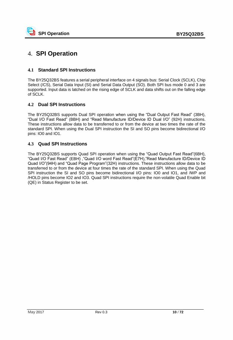
Read Data (03H) ..................................................................... 28
Fast Read (0BH) ..................................................................... 29
Dual Output Fast Read (3BH) ................................................. 30
Quad Output Fast Read (6BH) ................................................ 31

May 2017 Rev 0.3 3 / 72
Contents
NOR Flash Memory
NOR Flash Memory NOR Flash Memory
BY25Q32BS
Dual I/O Fast Read (BBH) ....................................................... 32
Quad I/O Fast Read (EBH)...................................................... 34
Quad I/O Word Fast Read (E7H) ............................................ 36
Set Burst with Wrap (77H) ....................................................... 38
7.3 ID and Security Instructions ....................................................................... 39
Read Manufacture ID/ Device ID (90H) ................................... 39
Dual I/O Read Manufacture ID/ Device ID (92H) ..................... 40
Quad I/O Read Manufacture ID/ Device ID (94H) ................... 41
Read JEDEC ID (9FH) ............................................................ 42
Read Unique ID Number (4Bh) ............................................... 43
Deep Power-Down (B9H) ........................................................ 44
Release from Deep Power-Down/Read Device ID (ABH) ....... 45
Read Security Registers (48H) ................................................ 46
Erase Security Registers (44H) ............................................... 47
Program Security Registers (42H) ........................................... 48
Enable Reset (66H) and Reset Device (99H) .......................... 49
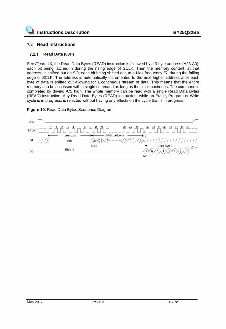
Read Serial Flash Discoverable Parameter (5AH) .................. 50
7.4 Program and Erase Instructions .................................................................. 51
Page Program (02H) ............................................................... 51
Quad Page Program (32H)...................................................... 52
Fast Page Program (F2H) ....................................................... 53
Sector Erase (20H) .................................................................. 54
32KB Block Erase (52H) ......................................................... 55
64KB Block Erase (D8H) ......................................................... 56
Chip Erase (60/C7H) ............................................................... 57
Erase / Program Suspend (75H) ............................................. 58
Erase / Program Resume (7AH) .............................................. 59
High Performance Mode (A3H) ............................................... 59
8. Electrical Characteristics .......................................................... 60
8.1 Absolute Maximum Ratings ....................................................................... 60
8.2 Operating Ranges ........................................................................................ 60
8.3 Data Retention and Endurance .................................................................... 60
8.4 Latch Up Characteristics ............................................................................. 61
8.5 Power-up Timing ......................................................................................... 61
8.6 DC Electrical Characteristics ...................................................................... 62
8.7 AC Measurement Conditions ...................................................................... 63
8.8 AC Electrical Characteristics ...................................................................... 63
9. Package Information ................................................................ 67
9.1 Package 8-Pin SOP 150-mil ........................................................................ 67
9.2 Package 8-Pin SOP 208-mil ........................................................................ 68
9.3 Package 8-Pin DIP8L .................................................................................. 69
9.4 Package 8-Pad WSON (6x5mm) ................................................................ 70
10. Order Information ..................................................................... 71
11. Document Change History ....................................................... 72

May 2017 Rev 0.3 4 / 72
Description
NOR Flash Memory
NOR Flash Memory NOR Flash Memory
BY25Q32BS
1. Description
The BY25Q32BS is 32M-bit Serial Peripheral Interface(SPI) Flash memory, and supports the Dual/Quad SPI: Serial Clock, Chip Select, Serial Data I/O0 (SI), I/O1 (SO), I/O2 (/WP), and I/O3 (/HOLD). The Dual I/O data is transferred with speed of 240Mbits/s and the Quad I/O & Quad output data is transferred with speed of 480Mbits/s. The device uses a single low voltage power supply, ranging from 2.7 Volt to 3.6 Volt.
Additionally, the device supports JEDEC standard manufacturer and device ID and three 256-bytes Security Registers.
In order to meet environmental requirements, Boya Microelectronics offers 8-pin SOP 208mil, 8-pad WSON 6x5-mm, and other special order packages, please contacts Boya Microelectronics for ordering information.
Figure 1. Logic diagram
BY25QXX
VCC
/HOLD
SCLK
SI
VSS
SO
/CS
/WP
Figure 2. Pin Configuration SOP 208 mil
1
2
3
4
8
7
6
5
Top View
SOP8 208mil
/CS
SO
/WP
VSS
VCC
/HOLD
SCLK
SI

May 2017 Rev 0.3 5 / 72
Description
NOR Flash Memory
NOR Flash Memory NOR Flash Memory
BY25Q32BS
Figure 3. Pin Configuration WSON 6x5-mm
1
2
3
4
8
7
6
5
Top View
/CS
SO
/WP
VSS
VCC
/HOLD
SCLK
SI

May 2017 Rev 0.3 6 / 72
Signal Description
NOR Flash Memory
NOR Flash Memory NOR Flash Memory
BY25Q32BS
2. Signal Description
During all operations, VCC must be held stable and within the specified valid range: VCC (min) to VCC (max).
All of the input and output signals must be held High or Low (according to voltages of VIH, VOH, VIL or VOL, see Section 8.6, DC Electrical Characteristics on page 59). These signals are described next.
2.1 Input/Output Summary
Table 1. Signal Names
2.2 Chip Select (/CS)
The chip select signal indicates when a instruction for the device is in process and the other signals are relevant for the memory device. When the /CS signal is at the logic high state, the device is not selected and all input signals are ignored and all output signals are high impedance. Unless an internal Program, Erase or Write Status Registers embedded operation is in progress, the device will be in the Standby Power mode. Driving the /CS input to logic low state enables the device, placing it in the Active Power mode. After Power Up, a falling edge on /CS is required prior to the start of any instruction.
2.3 Serial Clock (SCLK)
This input signal provides the synchronization reference for the SPI interface. Instructions, addresses, or data input are latched on the rising edge of the SCLK signal. Data output changes after the falling edge of SCLK.
Pin Name I/O Description
/CS I Chip Select
SO (IO1) I/O Serial Output for single bit data Instructions. IO1 for Dual or Quad Instructions.
/WP (IO2) I/O Write Protect in single bit or Dual data Instructions. IO2 in Quad mode. The signal has an internal pull-up resistor and may be left unconnected in the host system if not used for Quad Instructions.
VSS Ground
SI (IO0) I/O Serial Input for single bit data Instructions. IO0 for Dual or Quad Instructions.
SCLK I Serial Clock
/HOLD (IO3) I/O Hold (pause) serial transfer in single bit or Dual data Instructions. IO3 in Quad-I/O mode. The signal has an internal pull-up resistor and may be left unconnected in the host system if not used for Quad Instructions.
VCC Core and I/O Power Supply
NOR Flash Memory

May 2017 Rev 0.3 7 / 72
Signal Description
NOR Flash Memory
NOR Flash Memory NOR Flash Memory
BY25Q32BS
2.4 Serial Input (SI)/IO0
This input signal is used to transfer data serially into the device. It receives instructions, addresses, and data to be programmed. Values are latched on the rising edge of serial SCK clock signal.
SI becomes IO0 an input and output during Dual and Quad Instructions for receiving instructions, addresses, and data to be programmed (values latched on rising edge of serial SCK clock signal) as well as shifting out data (on the falling edge of SCK).
2.5 Serial Data Output (SO)/IO1
This output signal is used to transfer data serially out of the device. Data is shifted out on the falling edge of the serial SCK clock signal.
SO becomes IO1 an input and output during Dual and Quad Instructions for receiving instructions, addresses, and data to be programmed (values latched on rising edge of serial SCK clock signal) as well as shifting out data (on the falling edge of SCK).
2.6 Write Protect (/WP)/IO2
When /WP is driven Low (VIL), while the Status Register Protect bits (SRP1 and SRP0) of the Status Registers (SR2[0] and SR1[7]) are set to 0 and 1 respectively, it is not possible to write to the Status Registers. This prevents any alteration of the Status Registers. As a consequence, all the data bytes in the memory area that are protected by the Block Protect, TB, SEC, and CMP bits in the status registers, are also hardware protected against data modification while /WP remains Low. The /WP function is not available when the Quad mode is enabled (QE) in Status Register 2 (SR2[1]=1).
The /WP function is replaced by IO2 for input and output during Quad mode for receiving addresses, and data to be programmed (values are latched on rising edge of the SCK signal) as well as shifting out data (on the falling edge of SCK). /WP has an internal pull-up resistance; when unconnected; /WP is at VIH and may be left unconnected in the host system if not used for Quad mode.
2.7 HOLD (/HOLD)/IO3
The /HOLD function is only available when QE=0, If QE=1, The /HOLD function is disabled, the pin acts as dedicated data I/O pin
The /HOLD signal goes low to stop any serial communications with the device, but doesn’t stop the operation of write status register, programming, or erasing in progress.
The operation of HOLD, need /CS keep low, and starts on falling edge of the /HOLD signal, with SCLK signal being low (if SCLK is not being low, HOLD operation will not start until SCLK being low). The HOLD condition ends on rising edge of /HOLD signal with SCLK being low (If SCLK is not being low, HOLD operation will not end until SCLK being low).
The Hold condition starts on the falling edge of the Hold (/HOLD) signal, provided that this coincides with SCK being at the logic low state. If the falling edge does not coincide with the SCK signal being at the logic low state, the Hold condition starts whenever the SCK signal reaches the logic low state. Taking the /HOLD signal to the logic low state does not terminate any Write, Program or Erase operation that is currently in progress.

May 2017 Rev 0.3 8 / 72
Signal Description
NOR Flash Memory
NOR Flash Memory NOR Flash Memory
BY25Q32BS
HOLD HOLD
/CS
SCLK
/HOLD
2.8 VCC Power Supply
VCC is the supply voltage. It is the single voltage used for all device functions including read, program, and erase.
2.9 VSS Ground
VSS is the reference for the VCC supply voltage.

May 2017 Rev 0.3 9 / 72
Block/Sector Addresses
NOR Flash Memory
NOR Flash Memory NOR Flash Memory
BY25Q32BS
3. Block/Sector Addresses
Table 2. Block/Sector Addresses of BY25Q32BS
Memory Density
Block(64k byte)
Block(32k byte)
Sector No. Sector
Size(KB) Address range
32Mbit
Block 0
Half block 0
Sector 0 4 000000h-000FFFh
: : :
Sector 7 4 007000h-007FFFh
Half block 1
Sector 8 4 008000h-008FFFh
: 4 :
Sector 15 4 00F000h-00FFFFh
Block 1
Half block 2
Sector 16 4 010000h-010FFFh
: : :
Sector 23 4 017000h-017FFFh
Half block 3
Sector 24 4 018000h-018FFFh
: : :
Sector 31 4 01F000h-01FFFFh
: : : : :
Block 62
Half block 124
Sector 992 4 3E0000h-3E0FFFh
: : :
Sector 999 4 3E7000h-3E7FFFh
Half block 125
Sector 1000 4 3E8000h-3E8FFFh
: : :
Sector 1007 4 3EF000h-3EFFFFh
Block 63
Half block 126
Sector 1008 4 3F0000h-3F0FFFh
: : :
Sector 1015 4 3F7000h-3F7FFFh
Half block 127
Sector 1016 4 3F8000h-3F8FFFh
: : :
Sector 1023 4 3FF000h-3FFFFFh
Notes: 1. Block = Uniform Block, and the size is 64K bytes. 2. Half block = Half Uniform Block, and the size is 32k bytes. 3. Sector = Uniform Sector, and the size is 4K bytes.
May 2017 Rev 0.3 10 / 72
SPI Operation
NOR Flash Memory
NOR Flash Memory NOR Flash Memory
BY25Q32BS
4. SPI Operation
4.1 Standard SPI Instructions
The BY25Q32BS features a serial peripheral interface on 4 signals bus: Serial Clock (SCLK), Chip Select (/CS), Serial Data Input (SI) and Serial Data Output (SO). Both SPI bus mode 0 and 3 are supported. Input data is latched on the rising edge of SCLK and data shifts out on the falling edge of SCLK.
4.2 Dual SPI Instructions
The BY25Q32BS supports Dual SPI operation when using the “Dual Output Fast Read” (3BH), “Dual I/O Fast Read” (BBH) and “Read Manufacture ID/Device ID Dual I/O” (92H) instructions. These instructions allow data to be transferred to or from the device at two times the rate of the standard SPI. When using the Dual SPI instruction the SI and SO pins become bidirectional I/O pins: IO0 and IO1.
4.3 Quad SPI Instructions
The BY25Q32BS supports Quad SPI operation when using the “Quad Output Fast Read”(6BH), “Quad I/O Fast Read” (EBH) ,”Quad I/O word Fast Read”(E7H),”Read Manufacture ID/Device ID Quad I/O”(94H) and “Quad Page Program”(32H) instructions. These instructions allow data to be transferred to or from the device at four times the rate of the standard SPI. When using the Quad SPI instruction the SI and SO pins become bidirectional I/O pins: IO0 and IO1, and /WP and /HOLD pins become IO2 and IO3. Quad SPI instructions require the non-volatile Quad Enable bit (QE) in Status Register to be set.

May 2017 Rev 0.3 11 / 72
Operation Features
NOR Flash Memory
NOR Flash Memory NOR Flash Memory
BY25Q32BS
5. Operation Features
5.1 Supply Voltage
Operating Supply Voltage
Prior to selecting the memory and issuing instructions to it, a valid and stable VCC voltage within the specified [VCC(min), VCC(max)] range must be applied (see operating ranges of page 57). In order to secure a stable DC supply voltage, it is recommended to decouple the VCC line with a suitable capacitor (usually of the order of 10nF to 100nF) close to the VCC/VSS package pins. This voltage must remain stable and valid until the end of the transmission of the instruction and, for a Write instruction, until the completion of the internal write cycle (tW).

May 2017 Rev 0.3 12 / 72
Operation Features
NOR Flash Memory
NOR Flash Memory NOR Flash Memory
BY25Q32BS
Power-up Conditions
When the power supply is turned on, VCC rises continuously from VSS to VCC. During this time, the Chip Select (/CS) line is not allowed to float but should follow the VCC voltage, it is therefore recommended to connect the /CS line to VCC via a suitable pull-up resistor.
In addition, the Chip Select (/CS) input offers a built-in safety feature, as the /CS input is edge sensitive as well as level sensitive: after power-up, the device does not become selected until a falling edge has first been detected on Chip Select (/CS). This ensures that Chip Select (/CS) must have been High, prior to going Low to start the first operation.
Device Reset
In order to prevent inadvertent Write operations during power-up (continuous rise of VCC), a power on reset (POR) circuit is included. At Power-up, the device does not respond to any instruction until VCC has reached the power on reset threshold voltage (this threshold is lower than the minimum VCC operating voltage defined in operating ranges of page 57).
When VCC has passed the POR threshold, the device is reset.
Power-down
At Power-down (continuous decrease in VCC), as soon as VCC drops from the normal operating voltage to below the power on reset threshold voltage, the device stops responding to any instruction sent to it. During Power-down, the device must be deselected (Chip Select (/CS) should be allowed to follow the voltage applied on VCC) and in Standby Power mode (that is there should be no internal Write cycle in progress).
5.2 Active Power and Standby Power Modes
When Chip Select (/CS) is Low, the device is selected, and in the Active Power mode. The device consumes ICC.
When Chip Select (/CS) is High, the device is deselected. If a Write cycle is not currently in progress, the device then goes in to the Standby Power mode, and the device consumption drops to ICC1.
5.3 Hold Condition
The Hold (/HOLD) signal is used to pause any serial communications with the device without resetting the clocking sequence. During the Hold condition, the Serial Data Output (SO) is high impedance, and Serial Data Input (SI) and Serial Clock (SCLK) are Don’t Care. To enter the Hold condition, the device must be selected, with Chip Select (/CS) Low. Normally, the device is kept selected, for the whole duration of the Hold condition. Deselecting the device while it is in the Hold condition, has the effect of resetting the state of the device, and this mechanism can be used if it is required to reset any processes that had been in progress.
The Hold condition starts when the Hold (/HOLD) signal is driven Low at the same time as Serial Clock (SCLK) already being Low (as shown in Figure 4).

May 2017 Rev 0.3 13 / 72
Operation Features
NOR Flash Memory
NOR Flash Memory NOR Flash Memory
BY25Q32BS
The Hold condition ends when the Hold (HOLD) signal is driven High at the same time as Serial Clock (C) already being Low. Figure 4 also shows what happens if the rising and falling edges are not timed to coincide with Serial Clock (SCLK) being Low.
Figure 4. Hold condition activation
HOLD HOLD
/CS
SCLK
/HOLD
5.4 Status Register
Status Register Table
See Table 3 for detail description of the Status Register bits.
Table 3. Status Register
S23 S22 S21 S20 S19 S18 S17 S16
Reserved DRV1 DRV0 HPF Reserved Reserved Reserved Reserved
S15 S14 S13 S12 S11 S10 S9 S8
SUS1 CMP LB3 LB2 LB1 SUS2 QE SRP1
S7 S6 S5 S4 S3 S2 S1 S0
SRP0 BP4 BP3 BP2 BP1 BP0 WEL WIP

May 2017 Rev 0.3 14 / 72
Operation Features
NOR Flash Memory
NOR Flash Memory NOR Flash Memory
BY25Q32BS
The Status and Control Bits
5.4.2.1 WIP bit
The Write in Progress (WIP) bit indicates whether the memory is busy in program/erase/write status register progress. When WIP bit sets to 1, means the device is busy in program/erase/write status register progress, when WIP bit sets 0, means the device is not in program/erase/write status register progress.
5.4.2.2 WEL bit
The Write Enable Latch bit indicates the status of the internal Write Enable Latch. When set to 1 the internal Write Enable Latch is set, when set to 0 the internal Write Enable Latch is reset and no Write Status Register, Program or Erase instruction is accepted.
5.4.2.3 BP4, BP3, BP2, BP1, BP0 bits
The Block Protect (BP4, BP3, BP2, BP1, BP0) bits are non-volatile. They define the size of the area to be software protected against Program and Erase instructions. These bits are written with the Write Status Register instruction. When the Block Protect (BP4, BP3, BP2, BP1, BP0) bits are set to 1, the relevant memory area (as defined in Table 6 and Table 7).becomes protected against Page Program, Sector Erase and Block Erase instructions. The Block Protect (BP4, BP3, BP2, BP1, BP0) bits can be written provided that the Hardware Protected mode has not been set.The Chip Erase(CE) instruction is executed,if the Block Protect(BP2,BP1,BP0)bits are 0 and CMP=0 or The Block Protect (BP2, BP1, BP0) bits are1 and CMP=1.
5.4.2.4 SRP1, SRP0 bits
The Status Register Protect (SRP1 and SRP0) bits are non-volatile Read/Write bits in the status register. The SRP bits control the method of write protection: software protection, hardware protection, power supply lock-down or one time programmable protection.
5.4.2.5 QE bit
The Quad Enable (QE) bit is a non-volatile Read/Write bit in the Status Register that allows Quad operation. When the QE bit is set to 0 (Default) the /WP pin and /HOLD pin are enable. When the QE pin is set to 1, the Quad IO2 and IO3 pins are enabled. (The QE bit should never be set to 1 during standard SPI or Dual SPI operation if the /WP or /HOLD pins directly to the power supply or ground).
5.4.2.6 LB3/LB2/LB1 bit
The LB bit is a non-volatile One Time Program (OTP) bit in Status Register (S13–S11) that provide the write protect control and status to the Security Registers. The default state of LB is 0, the security registers are unlocked. LB can be set to 1 individually using the Write Register instruction. LB is One Time Programmable, once they are set to 1, the Security Registers will become read-only permanently.

May 2017 Rev 0.3 15 / 72
Operation Features
NOR Flash Memory
NOR Flash Memory NOR Flash Memory
BY25Q32BS
5.4.2.7 CMP bit
The CMP bit is a non-volatile Read/Write bit in the Status Register (S14). It is used in conjunction the SEC-BP0 bits to provide more flexibility for the array protection. Please see the Status registers Memory Protection table for details. The default setting is CMP=0.
5.4.2.8 SUS1/SUS2 bit
The SUS1 and SUS2 bits are read only bits in the status register2 (S15 and S10) that are set to 1 after executing an Erase/Program Suspend (75H) instruction (The Erase Suspend will set SUS1 to 1, and the Program Suspend will set the SUS2 to 1). The SUS1 and SUS2 bits are cleared to 0 by Erase/Program Resume (7AH) instruction as well as a power-down, power-up cycle.
5.4.2.9 HPF bit
The High Performance Flag bit indicates the status of High Performance Mode.When HPF bit sets to 1,it means the device is in High Performance Mode,when HPF bit sets to 0(Default),it means the device is not in High Performance Mode.
5.4.2.10 DRV1/DRV0
The DRV1&DRV0 bits are used to determine the output driver strength for the Read instruction.
Status Register Protect Table
The Status Register Protect (SRP1 and SRP0) bita are non-volatile Read/Write bits in the Status Register.The SRP bits control the morhod of write protection: software protection, hardware protection, power supply lock-down or one time programmable protection.
Table 4. Status Register protect table
SRP1 SRP0 /WP Status Register Description
0 0 X Software Protected
The Status Register can be written to after a Write Enable instruction, WEL=1.(Factory Default)
0 1 0 Hardware Protected
/WP=0, the Status Register locked and cannot be written.
0 1 1 Hardware
Unprotected /WP=1, the Status Register is unlocked and can be written to after a Write Enable instruction, WEL=1.
1 0 X Power Supply Lock-Down(1)
Status Register is protected and cannot be written to again until the next Power-Down, Power-Up cycle.
1 1 X One Time Program(2)
Status Register is permanently protected and cannot be written to.
DRV1,DRV0 Driver Strength
00 100%
01 75%(default)
10 50%
11 25%

May 2017 Rev 0.3 16 / 72
Operation Features
NOR Flash Memory
NOR Flash Memory NOR Flash Memory
BY25Q32BS
Notes:
1. When SRP1, SRP0= (1, 0), a Power-Down, Power-Up cycle will change SRP1, SRP0 to
(0, 0) state.
2. The One time Program feature is available upon special order. Please contact Boya
Microelectronics for details.

May 2017 Rev 0.3 17 / 72
Operation Features
NOR Flash Memory
NOR Flash Memory NOR Flash Memory
BY25Q32BS
Write Protect Features
1. Software Protection: The Block Protect (BP4, BP3, BP2, BP1, BP0) bits define the section of
the memory array that can be read but not change.
2. Hardware Protection: /WP going low to protected the writable bits of Status Register.
3. Deep Power-Down: In Deep Power-Down Mode, all instructions are ignored except the
Release from deep Power-Down Mode instruction.
4. Write Enable: The Write Enable instruction is set the Write Enable Latch bit.The WEL bit will
return to reset by following situation:
-Power –up
-Write Disable
-Write Status Register
-Page Program
-Sector Erase/Block Erase/Chip Erase
-Sofeware Reset

May 2017 Rev 0.3 18 / 72
Operation Features
NOR Flash Memory
NOR Flash Memory NOR Flash Memory
BY25Q32BS
Status Register Memory Protection
5.4.5.1 Protect Table
Table 5. BY25Q32BS Status Register Memory Protection (CMP=0)
Status Register Content Memory Content
BP4 BP3 BP2 BP1 BP0 Blocks Addresses Density Portion
X X 0 0 0 NONE NONE NONE NONE
0 0 0 0 1 63 3F0000H-3FFFFFH 64KB Upper 1/64
0 0 0 1 0 62 to 63 3E0000H-3FFFFFH 128KB Upper 1/32
0 0 0 1 1 60 to 63 3C0000H-3FFFFFH 256KB Upper 1/16
0 0 1 0 0 56 to 63 380000H-3FFFFFH 512KB Upper 1/8
0 0 1 0 1 48 to 63 300000H-3FFFFFH 1MB Upper 1/4
0 0 1 1 0 32 to 63 200000H-3FFFFFH 2MB Upper 1/2
0 1 0 0 1 0 000000H-00FFFFH 64KB Lower 1/64 0 1 0 1 0 0 to 1 000000H-01FFFFH 128KB Lower 1/32 0 1 0 1 1 0 to 3 000000H-03FFFFH 256KB Lower 1/16
0 1 1 0 0 0 to 7 000000H-07FFFFH 512KB Lower 1/8
0 1 1 0 1 0 to 15 000000H-0FFFFFH 1MB Lower 1/4
0 1 1 1 0 0 to 31 000000H-1FFFFFH 2MB Lower 1/2
X X 1 1 1 0 to 63 000000H-3FFFFFH 4MB ALL
1 0 0 0 1 63 3FF000H-3FFFFFH 4KB Top Block
1 0 0 1 0 63 3FE000H-3FFFFFH 8KB Top Block
1 0 0 1 1 63 3FC000H-3FFFFFH 16KB Top Block
1 0 1 0 X 63 3F8000H-3FFFFFH 32KB Top Block
1 0 1 1 0 63 3F8000H-3FFFFFH 32KB Top Block
1 1 0 0 1 0 000000H-000FFFH 4KB Bottom Block
1 1 0 1 0 0 000000H-001FFFH 8KB Bottom Block
1 1 0 1 1 0 000000H-003FFFH 16KB Bottom Block
1 1 1 0 X 0 000000H-007FFFH 32KB Bottom Block
1 1 1 1 0 0 000000H-007FFFH 32KB Bottom Block

May 2017 Rev 0.3 19 / 72
Operation Features
NOR Flash Memory
NOR Flash Memory NOR Flash Memory
BY25Q32BS
Table 6 BY25Q32BS Status Register Memory Protection (CMP=1)
Status Register Content Memory Content
BP4 BP3 BP2 BP1 BP0 Blocks Addresses Density Portion
X X 0 0 0 ALL 000000H-3FFFFFH 4MB ALL
0 0 0 0 1 0 to 62 000000H-3EFFFFH 4032KB Lower 63/64
0 0 0 1 0 0 to 61 000000H-3DFFFFH 3968KB Lower 31/32
0 0 0 1 1 0 to 59 000000H-3BFFFFH 3840KB Lower 15/16
0 0 1 0 0 0 to 55 000000H-37FFFFH 3584KB Lower r 7/8
0 0 1 0 1 0 to 47 000000H-2FFFFFH 3MB Lower 3/4
0 0 1 1 0 0 to 31 000000H-1FFFFFH 2MB Lower 1/2
0 1 0 0 1 1 to 63 010000H-3FFFFFH 4032KB Upper 63/64
0 1 0 1 0 2 to 63 020000H-3FFFFFH 3968KB Upper 31/32
0 1 0 1 1 4 to 63 040000H-3FFFFFH 3840KB Upper 15/16
0 1 1 0 0 8 to 63 080000H-3FFFFFH 3584KB Upper 7/8
0 1 1 0 1 16 to 63 100000H-3FFFFFH 3MB Upper 3/4
0 1 1 1 0 32 to 63 200000H-3FFFFFH 2MB Upper 1/2
X X 1 1 1 NONE NONE NONE NONE
1 0 0 0 1 0 to 63 000000H-3FEFFFH 4092KB L-1023/1024
1 0 0 1 0 0 to 63 000000H-3FDFFFH 4088KB L-511/512
1 0 0 1 1 0 to 63 000000H-3FBFFFH 4080KB L-255/256
1 0 1 0 X 0 to 63 000000H-3F7FFFH 4064KB L-127/128
1 0 1 1 0 0 to 63 000000H-3F7FFFH 4064KB L-127/128
1 1 0 0 1 0 to 63 001000H-3FFFFFH 4092KB U-1023/1024
1 1 0 1 0 0 to 63 002000H-3FFFFFH 4088KB U-511/512
1 1 0 1 1 0 to 63 004000H-3FFFFFH 4080KB U-255/256
1 1 1 0 X 0 to 63 008000H-3FFFFFH 4064KB U-127/128
1 1 1 1 0 0 to 63 008000H-3FFFFFH 4064KB U-127/128

May 2017 Rev 0.3 20 / 72
Device Identification
NOR Flash Memory
NOR Flash Memory NOR Flash Memory
BY25Q32BS
6. Device Identification
Three legacy Instructions are supported to access device identification that can indicate the manufacturer, device type, and capacity (density). The returned data bytes provide the information as shown in the below table.
Table 7. BY25Q32BS ID Definition table
Operation Code M7-M0 ID15-ID8 ID7-ID0
9FH 68 40 16
90H/92H/94H 68 15
ABH 15

May 2017 Rev 0.3 21 / 72
Instructions Description
NOR Flash Memory
NOR Flash Memory NOR Flash Memory
BY25Q32BS
7. Instructions Description
All instructions, addresses and data are shifted in and out of the device, beginning with the most significant bit on the first rising edge of SCLK after /CS is driven low. Then, the one byte instruction code must be shifted in to the device, most significant bit first on SI, each bit being latched on the rising edges of SCLK.
See Table 8, every instruction sequence starts with a one-byte instruction code. Depending on the instruction, this might be followed by address bytes, or by data bytes, or by both or none. /CS must be driven high after the last bit of the instruction sequence has been shifted in. For the instruction of Read, Fast Read, Read Status Register or Release from Deep Power Down, and Read Device ID, the shifted-in instruction sequence is followed by a data out sequence. /CS can be driven high after any bit of the data-out sequence is being shifted out.
For the instruction of Page Program, Sector Erase, Block Erase, Chip Erase, Write Status Register, Write Enable, Write Disable or Deep Power-Down instruction, /CS must be driven high exactly at a byte boundary, otherwise the instruction is rejected, and is not executed. That is /CS must driven high when the number of clock pulses after /CS being driven low is an exact multiple of eight. For Page Program, if at any time the input byte is not a full byte, nothing will happen and WEL will not be reset.

May 2017 Rev 0.3 22 / 72
Instructions Description
NOR Flash Memory
NOR Flash Memory NOR Flash Memory
BY25Q32BS
Table 8. Instruction Set Table
Instruction Name Byte 1 Byte 2 Byte 3 Byte 4 Byte 5 Byte 6 N-Bytes Write Enable 06H Write Disable 04H Read Status Register-1
05H (S7-S0) continuous
Read Status Register-2
35H (S15-S8) continuous
Read Status Register-3
15H (S23-S16) continuous
Write Enable for Volatile Status Register
50H
Write Status Register -1
01H (S7-S0)
Write Status Register-2
31H (S15-S8)
Write Status Register-3
11H (S23-S16)
Read Data 03H A23-A16 A15-A8 A7-A0 (D7-D0) Next byte
continuous
Fast Read 0BH A23-A16 A15-A8 A7-A0 dummy (D7-D0) continuous Dual Output Fast Read
3BH A23-A16 A15-A8 A7-A0 dummy (D7-D0)(1)
continuous
Dual I/O Fast Read BBH A23-A8(2) A7-A0
M7-M0(2) (D7-D0)(1) Next byte
Next byte
continuous
Quad Output Fast Read
6BH A23-A16 A15-A8 A7-A0 dummy (D7-D0)(3)
continuous
Quad I/O Fast Read EBH A23-A0
M7-M0(4) dummy(5) (D7-D0)(3) Next byte
Next byte
continuous
Quad I/O Word Fast Read(7)
E7H A23-A0
dM7-M0 (4) dummy(6) (D7-D0)(3) Next byte
Next byte
continuous
Page Program 02H A23-A16 A15-A8 A7-A0 (D7-D0) Next byte
continuous
Quad Page Program
32H A23-A16 A15-A8 A7-A0 (D7-D0)(3) Next byte
continuous
Fast Page Program F2H A23-A16 A15-A8 A7-A0 (D7-D0) Next byte
continuous
Sector Erase 20H A23-A16 A15-A8 A7-A0 Block Erase(32K) 52H A23-A16 A15-A8 A7-A0 Block Erase(64K) D8H A23-A16 A15-A8 A7-A0 Chip Erase C7/60H Enable Reset 66H Reset 99H Set Burst with Wrap 77H dummy(6)
W7-W0
Program/Erase Suspend
75H
Program/Erase Resume
7AH

May 2017 Rev 0.3 23 / 72
Instructions Description
NOR Flash Memory
NOR Flash Memory NOR Flash Memory
BY25Q32BS
Deep Power-Down B9H Release From Deep Power-Down, And Read Device ID
ABH dummy dummy dummy (ID7-ID0) continuous
Release From Deep Power-Down
ABH
Manufacturer/ Device ID
90H dummy dummy 00H (MID7-MID0) (ID7-ID0) continuous
Manufacturer/ Device ID by Dual I/O
92H A23-A8 A7-A0, dummy
(MID7-MID0),(DID7-DID0)
continuous
Manufacturer/ Device ID by Quad I/O
94H A23-A0, dummy
dummy(10)
(MID7-MID0)
(DID7-DID0)
continuous
JEDEC ID 9FH MID7-MID0
ID15-ID8 ID7-ID0 continuous
High Performance Mode
A3H dummy dummy dummy
Read Serial Flash Discoverable Parameter
5AH A23-A16 A15-A8 A7-A0 Dummy D7-D0
continuous
Erase Security Registers(8)
44H A23-A16 A15-A8 A7-A0
Program Security Registers(8)
42H A23-A16 A15-A8 A7-A0 (D7-D0) (D7-D0) continuous
Read Security Registers(8)
48H A23-A16 A15-A8 A7-A0 dummy (D7-D0) continuous
Notes:
1. Dual Output data IO0 = (D6, D4, D2, D0) IO1 = (D7, D5, D3, D1)
2. Dual Input Address IO0 = A22, A20, A18, A16, A14, A12, A10, A8, A6, A4, A2, A0, M6, M4, M2, M0 IO1 = A23, A21, A19, A17, A15, A13, A11, A9, A7, A5, A3, A1, M7, M5, M3,M1
3. Quad Output Data IO0 = (D4, D0,…..) IO1 = (D5, D1,…..) IO2 = (D6, D2,…..) IO3 = (D7, D3,…..)
4. Quad Input Address IO0 = A20, A16, A12, A8, A4, A0, M4, M0 IO1 = A21, A17, A13, A9, A5, A1, M5, M1 IO2 = A22, A18, A14, A10, A6, A2, M6, M2 IO3 = A23, A19, A15, A11, A7, A3, M7, M3
5. Fast Read Quad I/O Data IO0 = (x, x, x, x, D4, D0,…) IO1 = (x, x, x, x, D5, D1,…) IO2 = (x, x, x, x, D6, D2,…) IO3 = (x, x, x, x, D7, D3,…)
6. Fast Word Read Quad I/O Data

May 2017 Rev 0.3 24 / 72
Instructions Description
NOR Flash Memory
NOR Flash Memory NOR Flash Memory
BY25Q32BS
IO0 = (x, x, D4, D0,…) IO1 = (x, x , D5, D1,…) IO2 = (x, x, D6, D2,…) IO3 = (x, x, D7, D3,…)
7. Fast Word Read Quad I/O Data:the lowest address bit must be 0. 8. Security Registers Address:
Security Register1: A23-A16=00H, A15-A8=00010000b, A7-A0= Byte Address; Security Register2: A23-A16=00H, A15-A8=00100000b, A7-A0= Byte Address; Security Register3: A23-A16=00H, A15-A8=00110000b, A7-A0= Byte Address;
9. Dummy bits and Wraps Bits
IO0 = (x, x, x, x, x, x, w4, x) IO1 = (x, x, x, x, x, x, w5, x) IO2 = (x, x, x, x, x, x, w6, x) IO3 = (x, x, x, x, x, x, x,x)
10. Address, continuous Read Mode bits, Dummy bits, Manufacture ID and Device ID IO0 = (A20, A16, A12, A8, A4, A0, M4, M0, x, x, x, x, MID4, MID0, DID4, DID0) IO1 = (A21, A17, A13, A9, A5, A1, M5, M1, x, x, x, x, MID5, MID1, DID5, DID1) IO2 = (A22, A18, A14, A10, A6, A2, M6, M2, x, x, x, x, MID6, MID2, DID6, DID2) IO3 = (A23, A19, A15, A11, A7, A3, M7, M3, x, x, x, x, MID7, MID3, DID7, DID3)
Security Register 0 can be used to store the Flash Discoverable Parameters, The feature is upon special order, please contact Boya Microelectronics for details.

May 2017 Rev 0.3 25 / 72
Instructions Description
NOR Flash Memory
NOR Flash Memory NOR Flash Memory
BY25Q32BS
7.1 Configuration and Status Instructions
Write Enable (06H)
See Figure 5, the Write Enable instruction is for setting the Write Enable Latch bit. The Write Enable Latch bit must be set prior to every Page Program, Sector Erase, Block Erase, Chip Erase, Write Status Register instruction and Erase/Program Security Registers instruction. The Write Enable instruction sequence: /CS goes low sending the Write Enable instruction /CS goes high.
Figure 5. Write Enable Sequence Diagram
/CS
SCLK
SI
SOHigh_Z
06H
Instruction
0 1 2 3 4 5 6 7
Write Disable (04H)
See Figure 6, the Write Disable instruction is for resetting the Write Enable Latch bit. The Write Disable instruction sequence: /CS goes low -> sending the Write Disable instruction -> /CS goes high. The WEL bit is reset by following condition: Power-up and upon completion of the Write Status Register, Page Program, Sector Erase, Block Erase and Chip Erase, Erase/Program Security Registers and Reset instructions.
Figure 6. Write Disable Sequence Diagram
/CS
SCLK
SI
SOHigh_Z
04H
Instruction
0 1 2 3 4 5 6 7

May 2017 Rev 0.3 26 / 72
Instructions Description
NOR Flash Memory
NOR Flash Memory NOR Flash Memory
BY25Q32BS
Read Status Register (05H or 35H or 15H)
See Figure 7 the Read Status Register (RDSR) instruction is for reading the Status Register. The Status Register may be read at any time, even while a Program, Erase or Write Status Register cycle is in progress. When one of these cycles is in progress, it is recommended to check the Write in Progress (WIP) bit before sending a new instruction to the device. It is also possible to read the Status Register continuously. For instruction code “05H”, the SO will output Status Register bits S7~S0. The instruction code “35H”, the SO will output Status Register bits S15~S8, The instruction code “15H”, the SO will output Status Register bits S23~16.
Figure 7. Read Status Register Sequence Diagram
Instruction
05H or 35H or 15H
High_ZRegister 0/1/2 Register 0/1/2
7 6 5 4 3 2 1 0 7 6 5 4 3 2 1 0
MSB MSB
/CS
SCLK
SI
SO
0 1 2 3 4 5 6 7 8 9 10 11 12 13 14 15
Write Status Register (01H or 31H or 11H)
See Figure 8, the Write Status Register instruction allows new values to be written to the Status Register. Before it can be accepted, a Write Enable instruction must previously have been executed. After the Write Enable instruction has been decoded and executed, the device sets the Write Enable Latch (WEL).
The Write Status Register instruction has no effect on S23, S20, S19, S18, S17, S16, S15, S1 and S0 of the Status Register. /CS must be driven high after the eighth or sixteen bit of the data byte has been latched in. If not, the Write Status Register instruction is not executed. If /CS is driven high after eighth bit of the data byte, the CMP and QE and SRP1 bits will be cleared to 0. As soon as /CS is driven high, the self-timed Write Status Register cycle (whose duration is tW) is initiated. While the Write Status Register cycle is in progress, the Status Register may still be read to check the value of the Write in Progress (WIP) bit. The Write in Progress (WIP) bit is 1 during the self-timed Write Status Register cycle, and is 0 when it is completed. When the cycle is completed, the Write Enable Latch is reset.
The Write Status Register instruction allows the user to change the values of the Block Protect (BP4, BP3, BP2, BP1, BP0) bits, to define the size of the area that is to be treated as read-only, as defined in Table 3. The Write Status Register instruction also allows the user to set or reset the Status Register Protect (SRP1 and SRP0) bits in accordance with the Write Protect (/WP) signal. The Status Register Protect (SRP1 and SRP0) bits and Write Protect (/WP) signal allow the device to be put in the Hardware Protected Mode. The Write Status Register instruction is not executed once the Hardware Protected Mode is entered.

May 2017 Rev 0.3 27 / 72
Instructions Description
NOR Flash Memory
NOR Flash Memory NOR Flash Memory
BY25Q32BS
Figure 8. Write Status Register Sequence Diagram
Write Enable for Volatile Status Register (50H)
See Figure 9, the non-volatile Status Register bits can also be written to as volatile bits.. This gives more flexibility to change the system configuration and memory protection schemes quickly without waiting for the typical non-volatile bit write cycles or affecting the endurance of the Status Register non-volatile bits. Write Enable for Volatile Status Register instruction will not set the Write Enable Latch bit, it is only valid for the Write Status Registers instruction to change the volatile Status Register bit values.
Figure 9. Write Enable for Volatile Status Register
/CS
SCLK
SI
SOHigh_Z
50H
Instruction
0 1 2 3 4 5 6 7
0 1 2 3 4 5 6 7 8 9 10 11 12 13 14 15
Instruction
01H or 31H or 11H
Status Register in
7 6 5 4 3 2 1 0
High_Z
MSB
/CS
SCLK
SI
SO
May 2017 Rev 0.3 28 / 72
Instructions Description
NOR Flash Memory
NOR Flash Memory NOR Flash Memory
BY25Q32BS
7.2 Read Instructions
Read Data (03H)
See Figure 10, the Read Data Bytes (READ) instruction is followed by a 3-byte address (A23-A0), each bit being latched-in during the rising edge of SCLK. Then the memory content, at that address, is shifted out on SO, each bit being shifted out, at a Max frequency fR, during the falling edge of SCLK. The address is automatically incremented to the next higher address after each byte of data is shifted out allowing for a continuous stream of data. This means that the entire memory can be accessed with a single command as long as the clock continues. The command is completed by driving /CS high. The whole memory can be read with a single Read Data Bytes (READ) instruction. Any Read Data Bytes (READ) instruction, while an Erase, Program or Write cycle is in progress, is rejected without having any effects on the cycle that is in progress.
Figure 10. Read Data Bytes Sequence Diagram
0 1 2 3 4 5 6 7 8 9 10
Instruction
03H
24-Bit Address
2 1 0
MSB
High_Z
28 29 30 31 32 33 34 35 36 37 38 39
23 22 21 3
7 6 5 4 3 2 1 0
MSB
Data Byte1
/CS
SCLK
SI
SO
High_Z

May 2017 Rev 0.3 29 / 72
Instructions Description
NOR Flash Memory
NOR Flash Memory NOR Flash Memory
BY25Q32BS
Fast Read (0BH)
See Figure 11, the Read Data Bytes at Higher Speed (Fast Read) instruction is for quickly reading data out. It is followed by a 3-byte address (A23-A0) and a dummy byte, each bit being latched-in during the rising edge of SCLK. Then the memory content, at that address, is shifted out on SO, each bit being shifted out, at a Max frequency fc, during the falling edge of SCLK. The first byte addressed can be at any location. The address is automatically incremented to the next higher address after each byte of data is shifted out.
Figure 11. Fast Read Sequence Diagram
0 1 2 3 4 5 6 7 8 9 10
Instruction
0BH
24-Bit Address
2 1 0
High_Z
28 29 30 31
23 22 21 3
/CS
SCLK
32 33 34 35 36 37 38 39 40 41 42 43 44 45 46 47
Dummy Clocks
7 6 5 4 3 2 1 0
Data byte 1
/CS
SCLK
SOHigh_Z High_Z
SI
SI
SO
High_Z

May 2017 Rev 0.3 30 / 72
Instructions Description
NOR Flash Memory
NOR Flash Memory NOR Flash Memory
BY25Q32BS
Dual Output Fast Read (3BH)
See Figure 12, the Dual Output Fast Read instruction is followed by 3-byte address (A23-A0) and a dummy byte, each bit being latched in during the rising edge of SCLK, then the memory contents are shifted out 2-bit per clock cycle from SI and SO. The first byte addressed can be at any location. The address is automatically incremented to the next higher address after each byte of data is shifted out.
Figure 12. Dual Output Fast Read Sequence Diagram
0 1 2 3 4 5 6 7 8 9 10
Instruction
3BH
24-Bit Address
2 1 0
High_Z
28 29 30 31
23 22 21 3
32 33 34 35 36 37 38 39 40 41 42 43 44 45 46 47
Dummy Clocks
7 5 3 1 7 5
Data Byte 1
/CS
SCLK
SO
06 4 2 6 4 2 0
3 1
Data Byte 2
SI
SO
High_Z
/CS
SCLK
SI
High_Z
High_Z

May 2017 Rev 0.3 31 / 72
Instructions Description
NOR Flash Memory
NOR Flash Memory NOR Flash Memory
BY25Q32BS
Quad Output Fast Read (6BH)
See Figure 13, the Quad Output Fast Read instruction is followed by 3-byte address (A23-A0) and a dummy byte, each bit being latched in during the rising edge of SCLK, then the memory contents are shifted out 4-bit per clock cycle from IO3, IO2, IO1 and IO0. The first byte addressed can be at any location. The address is automatically incremented to the next higher address after each byte of data is shifted out.
Figure 13. Quad Output Fast Read Sequence Diagram
0 1 2 3 4 5 6 7 8 9 10
Instruction
6BH
24-Bit Address
2 1 0
High_Z
28 29 30 31
23 22 21 3
High_Z
High_Z
32 33 34 35 36 37 38 39 40 41 42 43 44 45 46 47
Dummy Clocks
4 0 4 0 4 0 4 0
5 1 5 1 5 1 5 1
6 2 6 2 6 2 6 2
7 3 7 3 7 3 7 3
Byte1 Byte2 Byte3 Byte4
/CS
SCLK
SI
(IO0)
SO(IO1)
/WP(IO2)
/HOLD(IO3)
/CS
SCLK
SI(IO0)
SO(IO1)
/WP(IO2)
/HOLD(IO3)
High_Z
High_Z
High_Z
High_Z
High_Z
High_Z
High_Z

May 2017 Rev 0.3 32 / 72
Instructions Description
NOR Flash Memory
NOR Flash Memory NOR Flash Memory
BY25Q32BS
Dual I/O Fast Read (BBH)
See Figure 14, the Dual I/O Fast Read instruction is similar to the Dual Output Fast Read instruction but with the capability to input the 3-byte address (A23-0) and a “Continuous Read Mode” byte 2-bit per clock by SI and SO, each bit being latched in during the rising edge of SCLK, then the memory contents are shifted out 2-bit per clock cycle from SI and SO. The first byte addressed can be at any location. The address is automatically incremented to the next higher address after each byte of data is shifted out.
Dual I/O Fast Read with“continuous Read Mode”
The Dual I/O Fast Read instruction can further reduce instruction overhead through setting the “continuous Read Mode”bits (M7-4) after the inputs 3-byte address A23-A0).If the “continuous Read Mode”bits(M5-4)=(1,0),then the next Dual I/O fast Read instruction (after CS/ is raised and thenlowered) does not require the BBH instruction code.The instruction sequence is shown in the
following Figure15.If the “continuous Read Mode”bits (M5-4) does not equal (1,0),the next
instruction requires the first BBH instruction code,thus returning to normal operation.A “continuous Read Mode” Reset instruction can be used to reset (M5-4) before issuing normal instruction.
Figure 14. Dual I/O Fast Read Sequence Diagram (Initial command or previous (M5-4)≠(1,0)))
0 1 2 3 4 5 6 7 8 9 10 11 12 13 14 15 16 17 18 19 20 21 22 23
Instruction
BBH 6 4 2 0 6 4 2 0 6 4 2 0 6 4 2 0
7 5 3 1 7 5 3 1 7 5 3 1 7 5 3 1
A23-16 A15-8 A7-0 M7-0
23 24 25 26 27 28 29 30 31 32 33 34 35 36 37 38 39
6 4 2 0 6 4 2 0 6 4 2 0 6 4 2 0
7 5 3 1 7 5 3 1 1 17 75 53 3
/CS
SCLK
SI(IO0)
SO(IO1)
/CS
SCLK
SI(IO0)
SO(IO1)
Byte 1 Byte 2 Byte 3 Byte 4
High_Z
High_Z
High_Z

May 2017 Rev 0.3 33 / 72
Instructions Description
NOR Flash Memory
NOR Flash Memory NOR Flash Memory
BY25Q32BS
Figure 15. Dual I/O Fast Read Sequence Diagram (Previous command set (M5-4) =(1,0))
0 1 2 3 4 5 6 7 8 9 10 11 12 13 14 15
6 6 6 64 4 4 4 2222 0 0 0 0
7 75 5 5 5 3333 1 1 17 71
A23-16 A15-8 A7-0 M7-0
15 16 17 18 19 20 21 22 23 24 25 26 27 28 29 30 31
6 6 6 64 4 4 4 2222 0 0 0 0
7 75 5 5 5 3333 1 1 17 71Byte1 Byte2 Byte3 Byte4
/CS
SCLK
/CS
SCLK
SI
(IO0)
SO(IO1)
SI(IO0)
SO(IO1)

May 2017 Rev 0.3 34 / 72
Instructions Description
NOR Flash Memory
NOR Flash Memory NOR Flash Memory
BY25Q32BS
Quad I/O Fast Read (EBH)
See Figure 16, the Quad I/O Fast Read instruction is similar to the Dual I/O Fast Read instruction but with the capability to input the 3-byte address (A23-0) and a “Continuous Read Mode” byte and 4-dummy clock 4-bit per clock by IO0, IO1, IO3, IO4, each bit being latched in during the rising edge of SCLK, then the memory contents are shifted out 4-bit per clock cycle from IO0, IO1, IO2, IO3. The first byte addressed can be at any location. The address is automatically incremented to the next higher address after each byte of data is shifted out. The Quad Enable bit (QE) of Status Register must be set to enable for the Quad I/O Fast read instruction. Quad I/O Fast Read with “Continuous Read Mode” The Quad I/O Fast Read instruction can further reduce instruction overhead through setting the “Continuous Read Mode” bits (M7-0) after the input Address bits (A23-0), as shown in Figure 16, If the “Continuous Read Mode” bits (M5-4 )= (1,0), then the next Fast Read Quad I/O instruction(after /CS is raised and then lowered) does not require the EBH instruction code, The instruction sequence is shown in the followed Figure 17. If the “Continuous Read Mode” bits M5-4 do not equal to (1,0), the next instruction requires the first EBH instruction code, thus returning to normal operation. A “Continuous Read Mode” Reset command can also be used to reset (M5-4) before issuing normal command.
Figure 16. Quad I/O Fast Read Sequence Diagram (Initial command or previous (M5-4≠(1,0)))
SCLK
SO(IO1)
/HOLD(IO3)
0 1 2 3 4 5 6 7 8 9 10 11
12 13 14 15 16 17 18 19 20 21 22 23
Instruction
EBH 4 0 4 4 4 4 4
5 1 5 1 5 5 5 51 1 1 1
6 6 66 6 62 2 2 2 2 2
7 3 7 7 7 7 7 33333
A23-16 A15-8 A7-0 Dummy Byte1 Byte2
0 0 0 0 0
/CS
/WP(IO2)
SI
(IO0)
High_Z
High_Z
High_Z

May 2017 Rev 0.3 35 / 72
Instructions Description
NOR Flash Memory
NOR Flash Memory NOR Flash Memory
BY25Q32BS
Figure 17. Quad I/O Fast Read Sequence Diagram (Previous command set (M5-4)=(1,0)))
0 1 2 3 4 5 6 7 8 9 10 11 12 13 14
4 0 4 4 4 4 4
1 5 1 5 5 5 51 1 1 1
6 6 66 6 62 2 2 2 2 2
7 3 7 7 7 7 7 33333
A15-8 A7-0 Dummy Byte1 Byte2
0 0 0 0 0
15
5
A23-16 M7-0
/CS
SCLK
SI
(IO0)
/WP(IO2)
/HOLD(IO3)
SO(IO1)
Quad I/O Fast Read with “8/16/32/64-Byte Wrap Around”
The Quad I/O Fast Read instruction can also be used to access a specific portion within a page by issuing a “Set Burst with Wrap” (77H) instruction prior to EBH. The “Set Burst with Wrap” (77H) instruction can either enable or disable the “Wrap Around” feature for the following EBH instructions. When “Wrap Around” is enabled, the data being accessed can be limited to either an 8, 16, 32 or 64-byte section of a 256-byte page. The output data starts at the initial address specified in the instruction, once it reaches the ending boundary of the 8/16/32/64-byte section, the output will wrap around to the beginning boundary automatically until /CS is pulled high to terminate the instruction.
The Burst with Wrap feature allows applications that use cache to quickly fetch a critical address and then fill the cache afterwards within a fixed length (8/16/32/64-byte) of data without issuing multiple read instructions.
The “Set Burst with Wrap” instruction allows three “Wrap Bits”, W6-4 to be set. The W4 bit is used to enable or disable the “Wrap Around” operation while W6-5 are used to specify the length of the wrap around section within a page.

May 2017 Rev 0.3 36 / 72
Instructions Description
NOR Flash Memory
NOR Flash Memory NOR Flash Memory
BY25Q32BS
Quad I/O Word Fast Read (E7H)
The Quad I/O Word Fast Read instruction is similar to the Quad Fast Read instruction except that the lowese address bit (A0) must equal 0 and 2-dummy clock. The instructionsequence is shown
in the followed Figure 18, the first byte addressed can bi at any location. The address is
automatically incremented to the next higher address after each byte of data is shifted out. The Quad Enable bit (QE) of Status Register (S9) must be set to enable for the Quad I/O Word Fast Read instruction. Quad I/O Word Fast Read with “Continuous Read Mode” The Quad I/O Word Fast Read instruction can further reduce instruction overhead through setting the “Continuous Read Mode” bits (M7-0) after the input 3-byte Address bits (A23-0). If the “Continuous Read Mode” bits (M5-4) = (1, 0), then the next Quad I/O Fast Read instruction (after /CS is raised and then lowered) does not require the E7H instruction code, the instruction
sequence is shown in the followed Figure 19. If the “Continuous Read Mode” bits M5-4 do not
equal to (1,0), the next instruction requires the first E7H instruction code, thus returning to normal operation. A “Continuous Read Mode” Reset command can also be used to reset (M5-4) before issuing normal command.
Figure 18. Quad I/O Word Fast Read Sequence Diagram (Initial command or previous (M5-4)≠
(1,0))
SCLK
SO(IO1)
/HOLD(IO3)
0 1 2 3 4 5 6 7 8 9 10 11
12 13 14 15 16 17 18 19 20 21 22 23
Instruction
E7H 4 0 4 4 4 4 4
5 1 5 1 5 5 5 51 1 1 1
6 6 66 6 62 2 2 2 2 2
7 3 7 7 7 7 7 33333
A23-16 A15-8 A7-0Dummy Byte2 Byte3
0 0 0 0 0
/CS
/WP(IO2)
SI(IO0)
High_Z
High_Z
High_Z
4
6
5
7 3
2
0
1
Byte1M7-M0

May 2017 Rev 0.3 37 / 72
Instructions Description
NOR Flash Memory
NOR Flash Memory NOR Flash Memory
BY25Q32BS
Figure 19. Quad I/O word Fast Read Sequence Diagram (Previous command set (M5-4) =(1,0))
Quad I/O Word Fast Read with “8/16/32/64-Byte Wrap Around” in standard SPI mode
The Quad I/O Fast Read instruction can also be used to access a specific portion within a page by issuing a “Set Burst with Wrap” (77H) instruction prior to E7H. The “Set Burst with Wrap” (77H) instruction can either enable or disable the “Wrap Around” feature for the following E7H instructions. When “Wrap Around” is enabled, the data being accessed can be limited to either an 8, 16, 32 or 64-byte section of a 256-byte page. The output data starts at the initial address specified in the instruction, once it reaches the ending boundary of the 8/16/32/64-byte section, the output will wrap around to the beginning boundary automatically until /CS is pulled high to terminate the instruction.
The Burst with Wrap feature allows applications that use cache to quickly fetch a critical address and then fill the cache afterwards within a fixed length (8/16/32/64-byte) of data without issuing multiple read instructions.
The “Set Burst with Wrap” instruction allows three “Wrap Bits”, W6-4 to be set. The W4 bit is used to enable or disable the “Wrap Around” operation while W6-5 are used to specify the length of the wrap around section within a page.
0 1 2 3 4 5 6 7 8 9 10 11 12 13 14
4 0 4 4 4 4 4
1 5 1 5 5 5 51 1 1 1
6 6 66 6 62 2 2 2 2 2
7 3 7 7 7 7 7 33333
A15-8 A7-0Dummy Byte1 Byte3
0 0 0 0 0
15
5
A23-16 M7-0
/CS
SCLK
SI
(IO0)
/WP(IO2)
/HOLD(IO3)
SO(IO1)
4 0
5 1
6 2
7 3
Byte2

May 2017 Rev 0.3 38 / 72
Instructions Description
NOR Flash Memory
NOR Flash Memory NOR Flash Memory
BY25Q32BS
Set Burst with Wrap (77H)
See Figure 20, The Set Burst with Wrap instruction is used in conjunction with”Quad I/O Fast Read” and “Quad I/O Word Fast Read” instruction to access a fixed length of 8/16/32/64-byte section within a 256-byte page,in standard SPI mode.
The Set Burst with Wrap instruction sequence:/CS goes low ->Send Set Burst with Wrap instruction ->Send24 Dummy bits ->Send 8 bits”Wrap bits”->/CS goes high.
If W6-4 is set by a Set Burst with Wrap instruction, all the following “Fast Read Quad I/O” and “Word Read Quad I/O” instructions will use the W6-4 setting to access the 8/16/32/64-byte section within any page. To exit the “Wrap Around” function and return to normal read operation, another Set Burst with Wrap instruction should be issued to set W4=1. The default value of W4 upon power on is 1.
W6 , W5
W4 = 0 W4 =1 (DEFAULT)
Wrap Around Wrap Length Wrap Around Wrap Length
0 0 Yes 8-byte No N/A
0 1 Yes 16-byte No N/A
1 0 Yes 32-byte No N/A
1 1 Yes 64-byte No N/A
Figure 20. Set Burst with Wrap Sequence Diagram
0 1 2 3 4 5 6 7 8 9 10 11 12 13 14 15
W4
W5
W6
Byte1 Byte2 Byte3 Byte4
/CS
SCLK
SI
(IO0)
SO(IO1)
/WP(IO2)
/HOLD(IO3)
High_Z
High_Z
High_Z
High_Z
High_Z
High_Z
High_Z
Instruction
77H x
x
x
x
x
x
x
x
x
x
x
x
x
x
x
x
x
x
x
x
x
x
x
x
x
x
x
xx

May 2017 Rev 0.3 39 / 72
Instructions Description
NOR Flash Memory
NOR Flash Memory NOR Flash Memory
BY25Q32BS
7.3 ID and Security Instructions
Read Manufacture ID/ Device ID (90H)
See Figure 21, The Read Manufacturer/Device ID instruction is an alternative to the Release from Power-Down/Device ID instruction that provides both the JEDEC assigned Manufacturer ID and the specific Device ID.
The instruction is initiated by driving the /CS pin low and shifting the instruction code “90H” followed by a 24-bit address (A23-A0) of 000000H. If the 24-bit address is initially set to 000001H, the Device ID will be read first.
Figure 21. Read Manufacture ID/ Device ID Sequence Diagram
0 1 2 3 4 5 6 7 8 9 10 28 29 30 31
Instruction
90H
High_Z
23 22 21 3 2 1 0
24-Bit Address
32 33 34 35 36 37 38 39 40 41 42 43 44 45 46 47
Device IDManufacturer ID
7 76 6 55 4 43 3 22 1 1 00
/CS
SCLK
SI
SO
SI
SCLK
SO
/CS

May 2017 Rev 0.3 40 / 72
Instructions Description
NOR Flash Memory
NOR Flash Memory NOR Flash Memory
BY25Q32BS
Dual I/O Read Manufacture ID/ Device ID (92H)
See Figure 22, the Dual I/O Read Manufacturer/Device ID instruction is an alternative to the Release from Power-Down/Device ID instruction that provides both the JEDEC assigned Manufacturer ID and the specific Device ID by Dual I/O.
The instruction is initiated by driving the /CS pin low and shifting the instruction code “92H” followed by a 24-bit address (A23-A0) of 000000H. If the 24-bit address is initially set to 000001H, the Device ID will be read first.
Figure 22. Dual I/O Read Manufacture ID/ Device ID Sequence Diagram
0 1 2 3 4 5 6 7 8 9 10 11 12 13 14 15 16 17 18 19 20 21 22 23
Instruction
92H 6 4 2 0 6 4 2 0 6 4 2 0 6 4 2 0
7 5 3 1 7 5 3 1 7 5 3 1 7 5 3 1
A23-16 A15-8 A7-0 Dummy
23 24 25 26 27 28 29 30 31 40 41 42 43 44 45 46 47
6 4 2 0 6 4 2 0 6 4 2 0 6 4 2 0
7 5 3 1 7 5 3 1 1 17 75 53 3
/CS
SCLK
SI(IO0)
SO(IO1)
/CS
SCLK
SI(IO0)
SO(IO1)
MFR ID Device ID
MFR and Device ID
(repeat) MFR ID(repeat)
High_Z
High_Z
High_Z
Device ID(repeat)
32 39

May 2017 Rev 0.3 41 / 72
Instructions Description
NOR Flash Memory
NOR Flash Memory NOR Flash Memory
BY25Q32BS
Quad I/O Read Manufacture ID/ Device ID (94H)
See Figure 23, the Quad I/O Read Manufacturer/Device ID instruction is an alternative to the Release from Power-Down/Device ID instruction that provides both the JEDEC assigned Manufacturer ID and the specific Device ID by quad I/O.
The instruction is initiated by driving the /CS pin low and shifting the instruction code “94H” followed by a 24-bit address (A23-A0) of 000000H and4 dummy clocks. If the 24-bit address is initially set to 000001H, the Device ID will be read first.
Figure 23. Quad I/O Read Manufacture ID/ Device ID Sequence Diagram
0 1 2 3 4 5 6 7 8 9 10 11 12 13 14 15 16 17 18 19 20 21 22 23
Instruction
94H 4 0 4 0 4 0 4 0
5 1 5 1 5 1 5 1
A23-16 A15-8 A7-0 dummy
23 24 25 26 27 28 29 30 31
/CS
SCLK
SI(IO0)
SO(IO1)
/CS
SCLK
SI(IO0)
SO(IO1)
High_Z
6 2 6 2 6 2 6 2WP
(IO2)
High_Z
7 3 7 3 7 3 7 3HOLD(IO3)
High_Z
MFR ID
(repeat)
WP(IO2)
HOLD(IO3)
4 0 4 0
5 1 5 1
6 2 6 2
7 3 7 3
dummy MFR ID Device ID
4 0 4 0 4 0 4 0
5 1 5 1 5 1 5 1
6 2 6 2 6 2 6 2
7 3 7 3 7 3 7 3
DID ID
(repeat)
MFR ID
(repeat)
DID ID
(repeat)

May 2017 Rev 0.3 42 / 72
Instructions Description
NOR Flash Memory
NOR Flash Memory NOR Flash Memory
BY25Q32BS
Read JEDEC ID (9FH)
The JEDEC ID instruction allows the 8-bit manufacturer identification to be read, followed by two bytes of device identification. The device identification indicates the memory type in the first byte, and the memory capacity of the device in the second byte. JEDEC ID instruction while an Erase or Program cycle is in progress, is not decoded, and has no effect on the cycle that is in progress. The JEDEC ID instruction should not be issued while the device is in Deep Power-Down Mode.
See Figure 24, The device is first selected by driving /CS to low. Then, the 8-bit instruction code for the instruction is shifted in. This is followed by the 24-bit device identification, stored in the memory, being shifted out on Serial Data Output, each bit being shifted out during the falling edge of Serial Clock. The JEDEC ID instruction is terminated by driving /CS to high at any time during data output. When /CS is driven high, the device is put in the Standby Mode. Once in the Standby Mode, the device waits to be selected, so that it can receive, decode and execute instructions.
Figure 24. JEDEC ID Sequence Diagram
0 1 2 3 4 5 6 7 8 9 10 11 12 13 14 15
16 17 18 19 20 21 22 23 24 25 26
27 28 29 30 31
7 6 5 4 3 2 1 0
Manufacturer ID
9FH
MSB
Memory Type ID15-ID8
MSB MSB
Capacity ID7-ID0
7 6 5 4 3 2 1 0 7 6 5 4 3 2 1 0
/CS
SCLK
SI
SO
/CS
SCLK
SI
SO
Instruction

May 2017 Rev 0.3 43 / 72
Instructions Description
NOR Flash Memory
NOR Flash Memory NOR Flash Memory
BY25Q32BS
Read Unique ID Number (4Bh)
The Read Unique ID Number instruction accesses a factory-set read-only 64-bit number that is unique to each BY25Q32 device. The ID number can be used in conjunction with user software methods to help prevent copying or cloning of a system. The Read Unique ID instruction is initiated by driving the /CS pin low and shifting the instruction code “4Bh” followed by a four bytes of dummy clocks. After which, the 64-bit ID is shifted out on the falling edge of SCLK as shown in Figure 25.
Figure 25. JEDEC ID Sequence Diagram
0 1 2 3 4 5 6 7
Mode 0
Mode 3
Instruction
/CS
SCLK
SI
SO
4BH
High_Z
8 9 10 11 12 13 14 15 16 17 18 19 20 21 22 23
Dummy Byte 1 Dummy Byte 2
Mode 0
Mode 325 26 27 28 2923
/CS
SCLK
SI
24 30
SO 6263
32 33 34 35 3631 37 39 40 41 100 10138 102
Dummy Byte 3 Dummy Byte 4
012High_Z
64-bit Unique Serial Number
MSB
103

May 2017 Rev 0.3 44 / 72
Instructions Description
NOR Flash Memory
NOR Flash Memory NOR Flash Memory
BY25Q32BS
Deep Power-Down (B9H)
Although the standby current during normal operation is relatively low, standby current can be further reduced with the Deep Power-down instruction. The lower power consumption makes the Deep Power-down (DPD) instruction especially useful for battery powered applications (see ICC1 and ICC2). The instruction is initiated by driving the /CS pin low and shifting the instruction code “B9h” as shown in Figure 26.
The /CS pin must be driven high after the eighth bit has been latched. If this is not done the Deep Power down instruction will not be executed. After /CS is driven high, the power-down state will entered within the time duration of tDP. While in the power-down state only the Release from Deep Power-down / Device ID instruction, which restores the device to normal operation, will be recognized. All other Instructions are ignored. This includes the Read Status Register instruction, which is always available during normal operation. Ignoring all but one instruction also makes the Power Down state a useful condition for securing maximum write protection. The device always powers-up in the normal operation with the standby current of ICC1.
Figure 26. Deep Power-Down Sequence Diagram
/CS
SCLK
SI
0 1 2 3 4 5 6 7
Instruction
B9H
tDP
Power-down modeStand-by mode

May 2017 Rev 0.3 45 / 72
Instructions Description
NOR Flash Memory
NOR Flash Memory NOR Flash Memory
BY25Q32BS
Release from Deep Power-Down/Read Device ID (ABH)
The Release from Power-Down or Device ID instruction is a multi-purpose instruction. It can be used to release the device from the Power-Down state or obtain the devices electronic identification (ID) number.
See Figure 27, to release the device from the Power-Down state, the instruction is issued by driving the /CS pin low, shifting the instruction code “ABH” and driving /CS high Release from Power-Down will take the time duration of tRES1 (See AC Characteristics) before the device will resume normal operation and other instruction are accepted. The /CS pin must remain high during the tRES1 time duration.
When used only to obtain the Device ID while not in the Power-Down state, the instruction is initiated by driving the /CS pin low and shifting the instruction code “ABH” followed by 3-dummy byte. The Device ID bits are then shifted out on the falling edge of SCLK with most significant bit (MSB) first as shown in Figure 28. The Device ID value for the BY25Q32BS is listed in Manufacturer and Device Identification table. The Device ID can be read continuously. The instruction is completed by driving /CS high.
When used to release the device from the Power-Down state and obtain the Device ID, the instruction is the same as previously described, and shown in Figure 28, except that after /CS is driven high it must remain high for a time duration of tRES2 (See AC Characteristics). After this time duration the device will resume normal operation and other instruction will be accepted. If the Release from Power-Down/Device ID instruction is issued while an Erase, Program or Write cycle is in process (when WIP equal 1) the instruction is ignored and will not have any effects on the current cycle.
Figure 27. Release Power-Down Sequence Diagram
/CS
SCLK
SI
0 1 2 3 4 5 6 7
Instruction
ABH
tRES1
Power-down mode Stand-by mode
Figure 28. Release Power-Down/Read Device ID Sequence Diagram
0 1 2 3 4 5 6 7 8 29 30 31 32 33 34 35 36 37 38
2
2
1
1
0
07 6 5 4 3
23 22
Instruction
ABH
3 Dummy Bytes
MSBHigh_Z
MSB
Device ID
tRES2
Deep Power-down mode Stand-by mode
/CS
SCLK
SI
SO
9 39

May 2017 Rev 0.3 46 / 72
Instructions Description
NOR Flash Memory
NOR Flash Memory NOR Flash Memory
BY25Q32BS
Read Security Registers (48H)
See Figure 29, the Read Security Registers instruction is similar to Fast Read instruction. The instruction is followed by a 3-byte address (A23-A0) and a dummy byte, each bit being latched-in during the rising edge of SCLK. Then the memory content, at that address, is shifted out on SO, each bit being shifted out, at a Max frequency fC, during the falling edge of SCLK. The first byte addressed can be at any location. The address is automatically incremented to the next higher address after each byte of data is shifted out. Once the A7-A0 address reaches the last byte of the register (Byte FFH), it will reset to 000H, the instruction is completed by driving /CS high.
Address A23-A16 A15-A12 A11-A8 A7-A0
Security Registers 1 00H 0001 0000 Byte Address
Security Registers 2 00H 0010 0000 Byte Address
Security Registers 3 00H 0011 0000 Byte Address
Figure 29. Read Security Registers instruction Sequence Diagram
/CS
SCLK
SI
0 1 2 3 4 5 6 7
Instruction
8 9 29 30 31
24-Bit Address
48H
28
SO High_Z
23 22 3 2 1 0
/CS
SCLK
SI
Dummy Byte
44 45 4643
SO
7 6 5 4 3 2 1 0
7 6 5 4 3 2 1 0
47
MSB
Data Byte 1
32 33 34 35 36 37 38 39 40 41 42

May 2017 Rev 0.3 47 / 72
Instructions Description
NOR Flash Memory
NOR Flash Memory NOR Flash Memory
BY25Q32BS
Erase Security Registers (44H)
The BY25Q32BS provides three 256-byte Security Registers which can be erased and programmed individually. These registers may be used by the system manufacturers to store security and other important information separately from the main memory array.
See Figure 30, the Erase Security Registers instruction is similar to Sector/Block Erase instruction. A Write Enable instruction must previously have been executed to set the Write Enable Latch bit.
The Erase Security Registers instruction sequence: /CS goes low sending Erase Security Registers instruction /CS goes high. /CS must be driven high after the eighth bit of the instruction code has been latched in otherwise the Erase Security Registers instruction is not executed. As soon as /CS is driven high, the self-timed Erase Security Registers cycle (whose duration is tSE) is initiated. While the Erase Security Registers cycle is in progress, the Status Register may be read to check the value of the Write In Progress (WIP) bit. The Write In Progress (WIP) bit is 1 during the self-timed Erase Security Registers cycle, and is 0 when it is completed. At some unspecified time before the cycle is completed, the Write Enable Latch bit is reset. The Security Registers Lock Bit (LB) in the Status Register can be used to OTP protect the security registers. Once the LB bit is set to 1, the Security Registers will be permanently locked; the Erase Security Registers instruction will be ignored.
Address A23-A16 A15-A12 A11-A8 A7-A0
Security Registers 1 00H 0001 0000 Byte Address
Security Registers 2 00H 0010 0000 Byte Address
Security Registers 3 00H 0011 0000 Byte Address
Figure 30. Erase Security Registers instruction Sequence Diagram
/CS
SCLK
SI 44H
Instruction
23 22 2 1 0
24-Bit Address
0 1 2 3 4 5 6 7 8 9 29 30 31

May 2017 Rev 0.3 48 / 72
Instructions Description
NOR Flash Memory
NOR Flash Memory NOR Flash Memory
BY25Q32BS
Program Security Registers (42H)
See Figure 31, the Program Security Registers instruction is similar to the Page Program instruction. It allows from 1 to 256 bytes Security Registers data to be programmed. A Write Enable instruction must previously have been executed to set the Write Enable Latch bit before sending the Program Security Registers instruction. The Program Security Registers instruction is entered by driving /CS Low, followed by the instruction code (42H), 3-byte address and at least one data byte on SI. As soon as /CS is driven high, the self-timed Program Security Registers cycle (whose duration is tPP) is initiated. While the Program Security Registers cycle is in progress, the Status Register may be read to check the value of the Write In Progress (WIP) bit. The Write In Progress (WIP) bit is 1 during the self-timed Program Security Registers cycle, and is 0 when it is completed. At some unspecified time before the cycle is completed, the Write Enable Latch bit is reset.
If the Security Registers Lock Bit (LB3/LB2/LB1) is set to 1, the Security Registers will be permanently locked. Program Security Registers instruction will be ignored.
Address A23-A16 A15-A12 A11-A8 A7-A0
Security Registers 1 00H 0001 0000 Byte Address
Security Registers 2 00H 0010 0000 Byte Address
Security Registers 3 00H 0011 0000 Byte Address
Figure 31. Program Security Registers instruction Sequence Diagram
0 1 2 3 4 5 6 7 8 9 10 28 29 30 31 32 33 34 35 36 37 38 39
Instruction
42H
MSB
23 2122 3 42 1 0 7 6 5 3 2 1 0
24-Bit Address Data Byte 1
MSB
40 41 42 43 44 45 46 47 48 49 50 51 52 53 54 55
Data Byte 256Data Byte 3Data Byte 2
7 7 7 666 5 5 54 4 4 333 2 2 21 1 1 000
MSB MSB MSB
/CS
SCLK
SI
/CS
SCLK
SI
2072
2073
2075
2076
2077
2078
2079
2074

May 2017 Rev 0.3 49 / 72
Instructions Description
NOR Flash Memory
NOR Flash Memory NOR Flash Memory
BY25Q32BS
Enable Reset (66H) and Reset Device (99H)
Because of the small package and the limitation on the number of pins, the BY25Q32BS provides
a software Reset instruction instead of a dedicated RESET pin. Once the software Reset
instruction is accepted, any on-going internal operations will be terminated and the device will
return to its default power-on state and lose all the current volatile settings, such as Volatile Status
Register bits, Write Enable Latch (WEL) status, Program/Erase Suspend status, Continuous Read
Mode bit setting (M7-M0) and Wrap Bit setting (W6-W4).
To avoid accidental reset, both “Enable Reset (66h)” and “Reset (99h)” instructions must be issued
in sequence. Any other commands other than “Reset (99h)” after the “Enable Reset (66h)”
command will disable the “Reset Enable” state. A new sequence of “Enable Reset (66h)” and
“Reset (99h)” is needed to reset the device. Once the Reset command is accepted by the device,
the device will take approximately 30us to reset. During this period, no command will be accepted.
The Enable Reset (66h) and Reset (99h) instruction sequence is shown in Figure 32.
Data corruption may happen if there is an on-going or suspended internal Erase or Program
operation when Reset command sequence is accepted by the device. It is recommended to check
the BUSY bit and the SUS bit in Status Register before issuing the Reset command sequence.
Figure 32. Enable Reset (66h) and Reset (99h) Command Sequence
/CS
SCLK
SI
0 1 2 3 4 5 6 7
66H
0 1 2 3 4 5 6 7
99h
Instruction Instruction
May 2017 Rev 0.3 50 / 72
Instructions Description
NOR Flash Memory
NOR Flash Memory NOR Flash Memory
BY25Q32BS
Read Serial Flash Discoverable Parameter (5AH)
See Figure 33,The Serial Flash Discoverable Parameter (SFDP) standard provides a consistent
method of describing the functional and feature capabilities of serial flash devices in a standard set
of internal parameter tables. These parameter tables can be interrogated by host system software
to enable adjustments needed to accommodate divergent features from multiple vendors. The
concept is similar to the one found in the Introduction of JEDEC Standard, JESD68 on CFI. SFDP
is a standard of JEDEC Standard No.216.
Figure 33. Read Serial Flash Discoverable Parameter command Sequence Diagram
/CS
SCLK
SI
0 1 2 3 4 5 6 7
Instruction
8 9 29 30 31
24-Bit Address
5AH
28
SO High_Z
23 22 3 2 1 0
/CS
SCLK
SI
Dummy Byte
44 45 4643
SO
7 6 5 4 3 2 1 0
7 6 5 4 3 2 1 0
47
MSB
Data Byte 1
32 33 34 35 36 37 38 39 40 41 42

May 2017 Rev 0.3 51 / 72
Instructions Description
NOR Flash Memory
NOR Flash Memory NOR Flash Memory
BY25Q32BS
7.4 Program and Erase Instructions
Page Program (02H)
The Page Program instruction is for programming the memory. A Write Enable instruction must previously have been executed to set the Write Enable Latch bit before sending the Page Program instruction.
See Figure 34, the Page Program instruction is entered by driving /CS Low, followed by the instruction code, 3-byte address and at least one data byte on SI. If the 8 least significant address bits (A7-A0) are not all zero, all transmitted data that goes beyond the end of the current page are programmed from the start address of the same page (from the address whose 8 least significant bits (A7-A0) are all zero). /CS must be driven low for the entire duration of the sequence. The Page Program instruction sequence: /CS goes low-> sending Page Program instruction ->3-byte address on SI ->at least 1 byte data on SI-> /CS goes high.
If more than 256 bytes are sent to the device, previously latched data are discarded and the last 256 data bytes are guaranteed to be programmed correctly within the same page. If less than 256 data bytes are sent to device, they are correctly programmed at the requested addresses without having any effects on the other bytes of the same page. /CS must be driven high after the eighth bit of the last data byte has been latched in; otherwise the Page Program instruction is not executed.
As soon as /CS is driven high, the self-timed Page Program cycle (whose duration is tPP) is initiated. While the Page Program cycle is in progress, the Status Register may be read to check the value of the Write in Progress (WIP) bit. The Write in Progress (WIP) bit is 1 during the self-timed Page Program cycle, and is 0 when it is completed. At some unspecified time before the cycle is completed, the Write Enable Latch bit is reset.
A Page Program instruction applied to a page which is protected by the Block Protect (BP4, BP3, BP2, BP1, BP0) bits (see Table 5&6) is not executed.
Figure 34. Page Program Sequence Diagram
0 1 2 3 4 5 6 7 8 9 10 28 29 30 31 32 33 34 35 36 37 38 39
Instruction
02H
MSB
23 2122 3 42 1 0 7 6 5 3 2 1 0
24-Bit Address Data Byte 1
MSB
40 41 42 43 44 45 46 47 48 49 50 51 52 53 54 55
Data Byte 256Data Byte 3Data Byte 2
7 7 7 666 5 5 54 4 4 333 2 2 21 1 1 000
MSB MSB MSB
/CS
SCLK
SI
/CS
SCLK
SI
2072
2073
2075
2076
2077
2078
2079
2074

May 2017 Rev 0.3 52 / 72
Instructions Description
NOR Flash Memory
NOR Flash Memory NOR Flash Memory
BY25Q32BS
Quad Page Program (32H)
The Quad Page Program instruction is for programming the memory using for pins: IO0, IO1, IO2 and IO3. To use Quad Page Program the Quad enable in status register Bit9 must be set (QE=1). A Write Enable instruction must previously have been executed to set the Write Enable Latch bit before sending the Page Program instruction. The Quad Page Program instruction is entered by driving /CS Low, followed by the command code (32H), three address bytes and at least one data byte on IO pins.
The instruction sequence is shown in Figure 35, .If more than 256 bytes are sent to the device, previously latched data are discarded and the last 256 data bytes are guaranteed to be programmed correctly within the same page. If less than 256 data bytes are sent to device, they are correctly programmed at the requested addresses without having any effects on the other bytes of the same page. /CS must be driven high after the eighth bit of the last data byte has been latched in; otherwise the Quad Page Program instruction is not executed.
As soon as /CS is driven high, the self-timed Quad Page Program cycle (whose duration is tPP) is initiated. While the Quad Page Program cycle is in progress, the Status Register may be read to check the value of the Write in Progress (WIP) bit. The Write In Progress (WIP) bit is 1 during the self-timed Quad Page Program cycle, and is 0 when it is completed. At some unspecified time before the cycle is completed, the Write Enable Latch bit is reset.A Quad Page Program instruction applied to a page which is protected by the Block Protect (BP4, BP3, BP2, BP1, BP0) bits (see Table 5&6) is not executed
Figure 35.Quad Page Program Sequence Diagrm
0 1 2 3 4 5 6 7 8 30 31 32 33 34 35 36 37 38 39
Instruction
32H 23 22 1 0 4 0 4 0 4 0 4 0
5 1 5 1 5 1 5 1
Byte1 Byte2
40 41 42 43 44 45 46 47 536 537 538 539 540 541 542 543
4 0 4 0 4 0 4 0 4 0 4 0 4 0 4 0
5 1 5 1 5 1 5 1 1 15 51 15 5
/CS
SCLK
SI(IO0)
SO(IO1)
/CS
SCLK
SI(IO0)
SO(IO1)
High_Z
High_Z
High_Z
48 535
6 2 6 2 6 2 6 2WP
(IO2)
High_Z
7 3 7 3 7 3 7 3HOLD(IO3)
High_Z
6 2 6 2 6 2 6 2 6 2 6 2 6 2 6 2
7 3 7 3 7 3 7 3 3 37 73 37 7
Byte 5 Byte 6 Byte 253
High_Z
High_Z
Byte 256
WP(IO2)
HOLD(IO3)
24-bits address

May 2017 Rev 0.3 53 / 72
Instructions Description
NOR Flash Memory
NOR Flash Memory NOR Flash Memory
BY25Q32BS
Fast Page Program (F2H)
The Fast Page Program instruction is used to program the memory. A Write Enable instruction must previously have been executed to set the Write Enable Latch bit before sending the Page Program instruction.
The Fast Page Program instruction is entered by driving /CS Low, followed by the instruction code, 3-byte address and at least one data byte on SI. If the 8 least significant address bits (A7-A0) are not all zero, all transmitted data that goes beyond the end of the current page are programmed from the start address of the same page (from the address whose 8 least significant bits (A7-A0) are all zero). /CS must be driven low for the entire duration of the sequence.
The Fast Page Program instruction sequence: /CS goes low ->sending Page Program instruction-> 3-byte address on SI-> at least 1 byte data on SI ->/CS goes high.
The command sequence is shown in Figure 36, If more than 256 bytes are sent to the device, previously latched data are discarded and the last 256 data bytes are guaranteed to be programmed correctly within the same page. If less than 256 data bytes are sent to device, they are correctly programmed at the requested addresses without having any effects on the other bytes of the same page. /CS must be driven high after the eighth bit of the last data byte has been latched in; otherwise the Fast Page Program instruction is not executed.
As soon as /CS is driven high, the self-timed Page Program cycle (whose duration is tPP) is initiated. While the Page Program cycle is in progress, the Status Register may be read to check the value of the Write in Progress (WIP) bit. The Write In Progress (WIP) bit is 1 during the self-timed Page Program cycle, and is 0 when it is completed. At some unspecified time before the cycle is completed, the Write Enable Latch bit is reset.
A Fast Page Program instruction applied to a page which is protected by the Block Protect (BP4, BP3, BP2, BP1, BP0) bits (see Table 5&6) is not executed.
Figure 36.Fast Page Program Sequence Diagram
0 1 2 3 4 5 6 7 8 9 10 28 29 30 31 32 33 34 35 36 37 38 39
Instruction
F2H
MSB
23 2122 3 42 1 0 7 6 5 3 2 1 0
24-Bit Address Data Byte 1
MSB
40 41 42 43 44 45 46 47 48 49 50 51 52 53 54 55
Data Byte 256Data Byte 3Data Byte 2
7 7 7 666 5 5 54 4 4 333 2 2 21 1 1 000
MSB MSB MSB
/CS
SCLK
SI
/CS
SCLK
SI
2072
2073
2075
2076
2077
2078
2079
2074

May 2017 Rev 0.3 54 / 72
Instructions Description
NOR Flash Memory
NOR Flash Memory NOR Flash Memory
BY25Q32BS
Sector Erase (20H)
The Sector Erase instruction is for erasing the all data of the chosen sector. A Write Enable instruction must previously have been executed to set the Write Enable Latch bit. The Sector Erase instruction is entered by driving /CS low, followed by the instruction code, and 3-address byte on SI. Any address inside the sector is a valid address for the Sector Erase instruction. /CS must be driven low for the entire duration of the sequence.
See Figure 37, The Sector Erase instruction sequence: /CS goes low-> sending Block Erase instruction-> 3-byte address on SI ->/CS goes high. /CS must be driven high after the eighth bit of the last address byte has been latched in; otherwise the Sector Erase instruction is not executed. As soon as /CS is driven high, the self-timed Sector Erase cycle (whose duration is tSE) is initiated. While the Sector Erase cycle is in progress, the Status Register may be read to check the value of the Write in Progress (WIP) bit. The Write in Progress (WIP) bit is 1 during the self-timed Sector Erase cycle, and is 0 when it is completed. At some unspecified time before the cycle is completed, the Write Enable Latch bit is reset. A Sector Erase instruction applied to a sector which is protected by the Block Protect (BP4, BP3, BP2, BP1, BP0) bits (see Table 5&6) is not executed.
Figure 37. Sector Erase Sequence Diagram
/CS
SCLK
SI 20H
Instruction
23 22 2 1 0
24-Bit Address
0 1 2 3 4 5 6 7 8 9 29 30 31

May 2017 Rev 0.3 55 / 72
Instructions Description
NOR Flash Memory
NOR Flash Memory NOR Flash Memory
BY25Q32BS
32KB Block Erase (52H)
The 32KB Block Erase instruction is for erasing the all data of the chosen block. A Write Enable instruction must previously have been executed to set the Write Enable Latch bit. The 32KB Block Erase instruction is entered by driving /CS low, followed by the instruction code, and 3-byte address on SI. Any address inside the block is a valid address for the 32KB Block Erase instruction. /CS must be driven low for the entire duration of the sequence.
See Figure 38, the 32KB Block Erase instruction sequence: /CS goes low ->sending 32KB Block Erase instruction ->3-byte address on SI ->/CS goes high. /CS must be driven high after the eighth bit of the last address byte has been latched in; otherwise the 32KB Block Erase instruction is not executed. As soon as /CS is driven high, the self-timed Block Erase cycle (whose duration is tBE) is initiated. While the Block Erase cycle is in progress, the Status Register may be read to check the value of the Write in Progress (WIP) bit. The Write In Progress (WIP) bit is 1 during the self-timed Block Erase cycle, and is 0 when it is completed. At some unspecified time before the cycle is completed, the Write Enable Latch bit is reset. A 32KB Block Erase instruction applied to a block which is protected by the Block Protect (BP4, BP3, BP2, BP1, BP0) bits (see Table 5&6) is not executed.
Figure 38. 32KB Block Erase Sequence Diagram
/CS
SCLK
SI 52H
Instruction
23 22 2 1 0
24-Bit Address
0 1 2 3 4 5 6 7 8 9 29 30 31

May 2017 Rev 0.3 56 / 72
Instructions Description
NOR Flash Memory
NOR Flash Memory NOR Flash Memory
BY25Q32BS
64KB Block Erase (D8H)
The 64KB Block Erase instruction is for erasing the all data of the chosen block. A Write Enable instruction must previously have been executed to set the Write Enable Latch bit. The 64KB Block Erase instruction is entered by driving /CS low, followed by the instruction code, and 3-byte address on SI. Any address inside the block is a valid address for the 64KB Block Erase instruction. /CS must be driven low for the entire duration of the sequence.
See Figure 39, the 64KB Block Erase instruction sequence: /CS goes low sending 64KB Block Erase instruction 3-byte address on SI /CS goes high. /CS must be driven high after the eighth bit of the last address byte has been latched in; otherwise the 64KB Block Erase instruction is not executed. As soon as /CS is driven high, the self-timed Block Erase cycle (whose duration is tBE) is initiated. While the Block Erase cycle is in progress, the Status Register may be read to check the value of the Write in Progress (WIP) bit. The Write in Progress (WIP) bit is 1 during the self-timed Block Erase cycle, and is 0 when it is completed. At some unspecified time before the cycle is completed, the Write Enable Latch bit is reset. A 64KB Block Erase instruction applied to a block which is protected by the Block Protect (BP4, BP3, BP2, BP1, BP0) bits (see Table 5&6) is not executed.
Figure 39 64KB Block Erase Sequence Diagram
/CS
SCLK
SI D8H
Instruction
23 22 2 1 0
24-Bit Address
0 1 2 3 4 5 6 7 8 9 29 30 31

May 2017 Rev 0.3 57 / 72
Instructions Description
NOR Flash Memory
NOR Flash Memory NOR Flash Memory
BY25Q32BS
Chip Erase (60/C7H)
The Chip Erase instruction sets all memory within the device to the erased state of all 1s (FFh). A Write Enable instruction must be executed before the device will accept the Chip Erase Instruction (Status Register bit WEL must equal 1). The instruction is initiated by driving the /CS pin low and shifting the instruction code “C7h” or “60h”. The Chip Erase instruction sequence is shown in Figure 40.
The /CS pin must be driven high after the eighth bit has been latched. If this is not done the Chip Erase instruction will not be executed. After /CS is driven high, the self-timed Chip Erase instruction will commence for a time duration of tCE. While the Chip Erase cycle is in progress, the Read Status Register instruction may still be accessed to check the status of the WIP bit.
The WIP bit is a 1 during the Chip Erase cycle and becomes a 0 when finished and the device is ready to accept other Instructions again. After the Chip Erase cycle has finished the Write Enable Latch (WEL) bit in the Status Register is cleared to 0. The Chip Erase instruction is executed only if all Block Protect (BP2, BP1, and BP0) bits are 0.The Chip Erase instruction is ignored if one or more sectors are protected.
Figure 40. Chip Erase Sequence Diagram
/CS
SCLK
SI
SOHigh_Z
60/C7H
Instruction
0 1 2 3 4 5 6 7

May 2017 Rev 0.3 58 / 72
Instructions Description
NOR Flash Memory
NOR Flash Memory NOR Flash Memory
BY25Q32BS
Erase / Program Suspend (75H)
The Erase/Program Suspend instruction allows the system to interrupt a Sector or Block Erase operation, then read from or program data to any other sector. The Erase/Program Suspend instruction also allows the system to interrupt a Page Program operation and then read from any other page or erase any other sector or block. The Erase/Program Suspend instruction sequence is shown in Figure 41
The Write Status Registers instruction (01h) and Erase instructions (20h, D8h, C7h, 60h, 44h) are not allowed during Erase Suspend. Erase Suspend is valid only during the Sector or Block erase operation. If written during the Chip Erase operation, the Erase Suspend instruction is ignored. The Write Status Registers instruction (01h), and Program instructions (02h, 42h) are not allowed during Program Suspend. Program Suspend is valid only during the Page Program operation.
Figure 41. Erase/Program Suspend Command Sequence
/CS
SCLK
SI
0 1 2 3 4 5 6 7
Instruction
75H
0 1 2 3 4 5 6 7
Instruction During Suspend
tSUS

May 2017 Rev 0.3 59 / 72
Instructions Description
NOR Flash Memory
NOR Flash Memory NOR Flash Memory
BY25Q32BS
Erase / Program Resume (7AH)
The Erase/Program Resume instruction “7Ah” must be written to resume the Sector or Block Erase operation or the Page Program operation after an Erase/Program Suspend. The Resume instruction “7AH” will be accepted by the device only if the SUS bit in the Status Register equals to 1 and the WIP bit equals to 0.
After the Resume instruction is issued the SUS bit will be cleared from 1 to 0 immediately, the WIP bit will be set from 0 to 1 within 200 ns and the Sector or Block will complete the erase operation or the page will complete the program operation. If the SUS bit equals to 0 or the WIP bit equals to 1, the Resume instruction “7Ah” will be ignored by the device. The Erase/Program Resume instruction sequence is shown in Figure 42.
Figure 42. Erase/Program Resume Command Sequence
/CS
SCLK
SI
SO High_Z
7AH
Instruction
0 1 2 3 4 5 6 7
High Performance Mode (A3H)
The High performance Mode instruction must be executed prior to Dual or Quad I/O instruction when operating at high frequencies(See fR and fc1 in AC Electrical Characteristics).This instruction allows pre-charing of internal charge pumps so the voltages required for accessing the flash memory array are readily available.The instruction sequence: /CS goes low ->Send A3H instruction ->Send 3 Dummy bytes -> /CS goes high.See Figure 43 .Agter the HPM command is executed,the device will maintain a slightly higher standby current(Icc9) than standard SPI instruction.The Release from Power-Down or HPM instruction (ABH) can be used to return to standard SPI standby current(Icc1).In addition,Power –Down instruction(B9H) will also release the device from HPM mode back to standard SPI standby state
Figure 43. High Performance Mode Sequence Diagram
0 1 2 3 4 5 6 7 8 9 10 28 29 30 31
Instruction
A3H
High_Z
23 22 21 3 2 1 0
3 dummy bytes
/CS
SCLK
SI
SO
tHPM
HPM

May 2017 Rev 0.3 60 / 72
Electrical Characteristics
NOR Flash Memory
NOR Flash Memory NOR Flash Memory
BY25Q32BS
8. Electrical Characteristics
8.1 Absolute Maximum Ratings
PARAMETERS SYMBOL CONDITIONS RANGE UNIT
Supply Voltage VCC –0.5 to 4 V
Voltage Applied to Any Pin VIO Relative to Ground –0.5 to 4 V
Transient Voltage on any Pin VIOT <20nS Transient
Relative to Ground –2.0V to VCC+2.0V V
Storage Temperature TSTG –65 to +150 °C
Electrostatic Discharge Voltage VESD Human Body Model(1) –2000 to +2000 V
Notes:
1. JEDEC Std JESD22-A114 (C1=100pF, R1=1500 ohms, R2=500 ohms)
8.2 Operating Ranges
PARAMETER SYMBOL CONDITIONS SPEC
UNIT MIN MAX
Supply Voltage VCC 2.7 3.6 V
Temperature Operating
TA Commercial
Industrial
0
–40
+70
+85 °C
8.3 Data Retention and Endurance
Parameter Test Condition Min Units
Minimum Pattern Data Retention Time 150°C 10 Years
125°C 20 Years
Erase/Program Endurance -40 to 85°C 100K Cycles

May 2017 Rev 0.3 61 / 72
Electrical Characteristics
NOR Flash Memory
NOR Flash Memory NOR Flash Memory
BY25Q32BS
8.4 Latch Up Characteristics
Parameter Min Max
Input Voltage Respect To VSS On I/O Pins -1.0V VCC+1.0V
VCC Current -100mA 100mA
8.5 Power-up Timing
Symbol Parameter Min Max Unit
tVSL VCC(min) To /CS Low 300 us
Figure 44. Power-up Timing and Voltage Levels
Time
Vcc(min)
Vcc(max)
Chip selection is not allowed
tVSLDevice is fully
accessible

May 2017 Rev 0.3 62 / 72
Electrical Characteristics
NOR Flash Memory
NOR Flash Memory NOR Flash Memory
BY25Q32BS
8.6 DC Electrical Characteristics
(T= -40℃~85℃, VCC=2.7~3.6V)
Symbol Parameter Test Condition Min. Typ Max. Unit.
ILI Input Leakage Current
±2 µA
ILO Output Leakage Current
±2 µA
ICC1 Standby Current /CS=VCC,
VIN=VCC or VSS 13 25 µA
ICC2 Deep Power-Down Current
/CS=VCC, VIN=VCC or VSS
2 5 µA
ICC3 Operating Current: (Read)
SCLK=0.1VCC/ 0.9VCC, at
120MHz,Q=Open(*1,*,2*4 I/O)
15 20 mA
SCLK=0.1VCC/ 0.9VCC, at
80MHz,Q=Open(*1,*,2*4 I/O)
13 18 mA
ICC4 Operating Current(Page Program)
/CS=VCC 15 mA
ICC5 Operating Current(WRSR)
/CS=VCC 5 mA
ICC6 Operating Current(Sector Erase)
/CS=VCC 20 mA
ICC7 Operating Current(Block Erase)
/CS=VCC 20 mA
ICC8 Operating Current (Chip Erase)
/CS=VCC 20 mA
ICC9 High performance current 400 800 uA
VIL Input Low Voltage -0.5 0.2VCC V
VIH Input High Voltage 0.8VCC VCC+0.4 V
VOL Output Low Voltage
IOL =100µA 0.4 V
VOH Output High Voltage
IOH =-100µA VCC-0.2 V

May 2017 Rev 0.3 63 / 72
Electrical Characteristics
NOR Flash Memory
NOR Flash Memory NOR Flash Memory
BY25Q32BS
8.7 AC Measurement Conditions
Symbol Parameter Min Tpy Max Unit Conditions
CL Load Capacitance 30 pF
TR, TF Input Rise And Fall time 5 ns
VIN Input Pause Voltage 0.2VCC to 0.8VCC V
IN Input Timing Reference Voltage 0.5VCC V
OUT Output Timing Reference Voltage 0.5VCC V
Figure 45. AC Measurement I/O Waveform
0.8VCC
0.2VCC
0.5VCC 0.5VCC
Input Levels
Output Timing
Reference Levels
Input Timing
Reference Levels
8.8 AC Electrical Characteristics
Symbol Parameter Min. Typ. Max. Unit.
Fc
Clock frequency for Dual I/O(BBH),Quad I/O(EBH),Quad output(6BH)(Dual I/O & Quad I/O without High Performance Mode) on 3.0v-3.6v power supply
DC. 104 MHz
Fc1
Clock frequency for Dual I/O(BBH),Quad I/O(EBH),Quad output(6BH)(Dual I/O & Quad I/O without High Performance Mode) on 2.7v-3.0v power supply
DC. 80 MHz
Fc2 Clock frequency for Dual I/O(BBH),Quad I/O(EBH),Quad output(6BH)(Dual I/O &Quad I/O with High Performance Mode) on 2.7v-3.6v power supply
DC. 120 MHz
fR Clock freq. for Read Data instruction (03H) and other non-read instructions.
DC. 55 MHz
tCLH Serial Clock High Time 4 ns
tCLL Serial Clock Low Time 4 ns
tCLCH Serial Clock Rise Time (Slew Rate) 0.1(1) V/ns
tCHCL Serial Clock Fall Time (Slew Rate) 0.1(1) V/ns
tSLCH /CS Active Setup Time 5 ns
tCHSH /CS Active Hold Time 5 ns
tSHCH /CS Not Active Setup Time 5 ns

May 2017 Rev 0.3 64 / 72
Electrical Characteristics
NOR Flash Memory
NOR Flash Memory NOR Flash Memory
BY25Q32BS
tCHSL /CS Not Active Hold Time 5 ns
Symbol Parameter Min. Typ. Max. Unit.
tSHSL /CS High Time(read/write) 20 ns
tSHQZ Output Disable Time 6 ns
tCLQX Output Hold Time 0 ns
tDVCH Data In Setup Time 2 ns
tCHDX Data In Hold Time 2 ns
tHLCH /Hold Low Setup Time (relative to Clock) 5 ns
tHHCH /Hold High Setup Time (relative to Clock) 5 ns
tCHHL /Hold High Hold Time (relative to Clock) 5 ns
tCHHH /Hold Low Hold Time (relative to Clock) 5 ns
tHLQZ /Hold Low To High-Z Output 6 ns
tHHQX /Hold Low To Low-Z Output 6 ns
tCLQV Clock Low To Output Valid 7 ns
tWHSL Write Protect Setup Time Before /CS Low 20 ns
tSHWL Write Protect Hold Time After /CS High 100 ns
tDP /CS High To Deep Power-Down Mode 20 µs
tRES1 /CS High To Standby Mode Without Electronic Signature Read 20 µs
tRES2 /CS High To Standby Mode With Electronic Signature Read 20 µs
tSUS /CS High To Next Instruction After Suspend 20 µs
tRST_R /CS High To Next Instruction After Reset(from read) 20
tRST_P /CS High To Next Instruction After Reset(from program) 20
tRST_E /CS High To Next Instruction After Reset(from erase) 12
tW Write Status Register Cycle Time 5 30(2) ms
tBP1 Byte Program Time (First Byte) (3) 30 50 µs
tBP2 Additional Byte Program Time (After First Byte) (3) 2.5 12 µs
tPP Page Programming Time 0.6 2.4 ms
tSE Sector Erase Time 50 300 ms
tBE Block Erase Time(32K Bytes/64K Bytes) 0.15/0.25 1.6/2 S
tCE Chip Erase Time 15 30 S
Note:
1. Tested with clock frequency lower than 50 MHz.

May 2017 Rev 0.3 65 / 72
Electrical Characteristics
NOR Flash Memory
NOR Flash Memory NOR Flash Memory
BY25Q32BS
2. For multiple bytes after first byte within a page, tBPn = tBP1 + tBP2 * N, where N is the number of bytes programmed.
Figure 46. Serial inputTiming
SCLK
SI
SO
LSB
/CS
tSHSL
tCHSL
tSLCH
tSHCH
tCHCLtCLCH
tCHSH
MSB
tDVCHtCHDX
High_Z
Figure 47. Output Timing
SCLK
SO
tCH
tQLQH
SI
LSB
tCLQV
tCLQX
tCLQV
tCLQX
/CS
tCL
tSHQZ
tQHQL
Figure 48. Hold Timing
tCHHL
SCLK
SO
/CS
tHLCH
tHLQZtCHHH
tHHCH
tHHQX
/HOLD

May 2017 Rev 0.3 66 / 72
Electrical Characteristics
NOR Flash Memory
NOR Flash Memory NOR Flash Memory
BY25Q32BS
Figure 49. /WP Timing

May 2017 Rev 0.3 67 / 72
PACKAGE INFORMATION
NOR Flash Memory
NOR Flash Memory NOR Flash Memory
BY25Q32BS
9. Package Information
9.1 Package 8-Pin SOP 150-mil
E
8 5
1 4
E1
θ
L1L
D
beS
A
A1
A2
C
Dimensions
Symbol A A1 A2 b C D E E1 e L L1 S θ
Unit
mm
Min 0.10 1.35 0.36 0.15 4.77 5.80 3.80 0.46 0.85 0.41 0
Nom 0.15 1.45 0.41 0.20 4.90 5.99 3.90 1.27 0.66 1.05 0.54 5
Max 1.75 0.20 1.55 0.51 0.25 5.03 6.20 4.00 0.86 1.25 0.67 8
Inch
Min 0.004 0.053 0.014 0.006 0.188 0.228 0.150 0.018 0.033 0.016 0
Nom 0.006 0.057 0.016 0.008 0.193 0.236 0.154 0.05 0.026 0.041 0.021 5
Max 0.069 0.008 0.061 0.020 0.010 0.198 0.244 0.158 0.034 0.049 0.026 8

May 2017 Rev 0.3 68 / 72
PACKAGE INFORMATION
NOR Flash Memory
NOR Flash Memory NOR Flash Memory
BY25Q32BS
9.2 Package 8-Pin SOP 208-mil
E
8 5
1 4
E1
θ
L1L
D
beS
A
A1
A2
C
Dimensions
Symbol A A1 A2 b C D E E1 e L L1 S è
Unit
mm
Min 0.05 1.70 0.36 0.19 5.13 7.70 5.18 0.50 1.21 0.62 0
Nom 0.15 1.80 0.41 0.20 5.23 7.90 5.28 1.27 0.65 1.31 0.74 5
Max 2.16 0.25 1.91 0.51 0.25 5.33 8.10 5.38 0.80 1.41 0.88 8
Inch
Min 0.002 0.067 0.014 0.007 0.202 0.303 0.204 0.020 0.048 0.024 0
Nom 0.006 0.071 0.016 0.008 0.206 0.311 0.208 0.050 0.026 0.052 0.029 5
Max 0.085 0.010 0.075 0.020 0.010 0.210 0.319 0.212 0.031 0.056 0.035 8
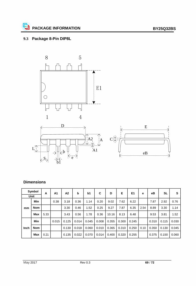
May 2017 Rev 0.3 69 / 72
PACKAGE INFORMATION
NOR Flash Memory
NOR Flash Memory NOR Flash Memory
BY25Q32BS
9.3 Package 8-Pin DIP8L
D
b
eS
A
A1
A2
L
b1
5
E1
8
1 4
E
C
eB
Dimensions
Symbol A A1 A2 b b1 C D E E1 e eB SL S
Unit
mm
Min 0.38 3.18 0.36 1.14 0.20 9.02 7.62 6.22 7.87 2.92 0.76
Nom 3.30 0.46 1.52 0.25 9.27 7.87 6.35 2.54 8.89 3.30 1.14
Max 5.33 3.43 0.56 1.78 0.36 10.16 8.13 6.48 9.53 3.81 1.52
Inch
Min 0.015 0.125 0.014 0.045 0.008 0.355 0.300 0.245 0.310 0.115 0.030
Nom 0.130 0.018 0.060 0.010 0.365 0.310 0.250 0.10 0.350 0.130 0.045
Max 0.21 0.135 0.022 0.070 0.014 0.400 0.320 0.255 0.375 0.150 0.060

May 2017 Rev 0.3 70 / 72
PACKAGE INFORMATION
NOR Flash Memory
NOR Flash Memory NOR Flash Memory
BY25Q32BS
9.4 Package 8-Pad WSON (6x5mm)
1
45
8
L
b
e
D1
E1
E
DA
A1y
A2
Dimensions
Symbol A A1 A2 b D D1 E E1 e y L
Unit
mm
Min 0.70 0.19 0.35 5.90 3.25 4.90 3.85 0.00 0.50
Nom 0.75 0.22 0.42 6.00 3.37 5.00 3.97 1.27 0.04 0.60
Max 0.80 0.05 0.25 0.48 6.10 3.50 5.10 4.10 0.08 0.75
Inch
Min 0.028 0.007 0.014 0.232 0.128 0.193 0.151 0.000 0.020
Nom 0.030 0.009 0.016 0.236 0.133 0.197 0.156 0. 05 0.001 0.024
Max 0.032 0.002 0.010 0.019 0.240 0.138 0.201 0.161 0.003 0.030

May 2017 Rev 0.3 71 / 72
Order Information
NOR Flash Memory
NOR Flash Memory NOR Flash Memory
BY25Q32BS
10. Order Information
BY 25Q 32 B S S I G
Green Code
P:Pb Free Only Green Package
G:Pb Free & Halogen Free Green Package
Temperature Range
C:Commercial(0°C to +70°C)
I:Industrial(-40°C to +85°C)
Package Type
S:SOP8 208mil
W:WSON 6x5-mm
Voltage
S:3V
L:1.8V
Generation
A:A Version
B:B Version
C:C Version
Density
80:8Mbit
16:16Mbit
32:32Mbit
Product Family
25Q:SPI Interface Flash

May 2017 Rev 0.3 72 / 72
Document Change History
NOR Flash Memory
NOR Flash Memory NOR Flash Memory
BY25Q32BS
11. Document Change History
Doc. Rev.
Tech Dev. Rev.
Effective Date
Change Description
0.0 2016-12-29 Initiate
0.1 2017-2-7 Update Power-up Timing
0.2 2017-4-13 Add Read Unique ID Number(4BH) Instruction
0.3 2017-5-2 Update AC Measurement Conditions,Serial Input&output Timing