Embed Size (px)
Citation preview

RGB ELEKTRONIKA AGACIAK CIACIEKSPÓŁKA JAWNA Jana Dlugosza 2-6 Street51-162 WrocławPoland
[email protected] +48 71 325 15 05
www.rgbautomatyka.pl
www.rgbelektronika.pl
DATASHEET
www.rgbautomatyka.plwww.rgbelektronika.pl
OTHER SYMBOLS:
LQ10D42
SHARP

YOUR PARTNER IN MAINTENANCE
At our premises in Wrocław, we have a fully equipped servicing facility. Here we perform all the repair works and test each later sold unit. Our trained employees, equipped with a wide variety of tools and having several testing stands at their disposal, are a guarantee of the highest quality service.
OUR SERVICES
ENCODERS
SERVO DRIVERS
LINEAR ENCODERS
SERVO AMPLIFIERS
CNC MACHINES
MOTORS
POWER SUPPLIERS
OPERATOR PANELS
CNC CONTROLS
INDUSTRIAL COMPUTERS
PLC SYSTEMS
Repair this product with RGB ELEKTRONIKA ORDER A DIAGNOSIS �
Buy this product at RGB AUTOMATYKA BUY �

TECHNICAL LITERATURE
FOR
TFT-LCD module
MODEL No. LQ1O’D42
TENTATIVE
I The technical literature is subject to change without notice.
E Sharp or its representative before designing
on this literature.
SHARP CORPORATIONTENRILCD
LIQUID CRYSTAL DISPLAY GROUPPRODUCTS DEVELOPMENT CENTER

,,.
RECORDS OF REVISION’M O D E L “ N o : LQ1OD42
S P E C No :LD–8258
DATE REVISED SUMMARY NOTE
No. PAGE
1996. 3.12 - - 1 st Issue
1996. 5. 7 A Cover Change :Department of issue-- - --- - -— -——-- ----—-—--——-—--- - - - - - - - - - - - - - - - - - —-- --—--------—
2 Addition:’’Haze value=28%-- ---——-— - - - - - ----—- - - - - - - - - - - - - - - - - - - - - - - - - - - - — — - - - - - - - - - - - - -
6 Change :Kick-off voltage- - - - - ---— - - - - - - - - - - - — - —-- - -- -- - - --- -- - - - - - - -- - ---- - - - - - - - - - - - -
l100+950Vrms(Ta=25”c)---—----— -——- ---— .---— - - - -- - - --- -------—---—-——- —--.————————1300+1400Vrms(Ta=O”c)
-------—— - - - - .--—-— --- - —-- - - ——- - -- -- - --------—---- - - - - - - - - - - - -
-------—- - - - - -----— - - - - — - - - - - - - - - - - - - - - - - - - - - - - - - - - - - - - - - - - _ _ _
- - - - - - —- - -—-- - - - - - - - — — - — - - - - - - — - - - - - - - - - - - — - - - - - - - - - - - - - -- - - --
-------—— -——- ——-— ----—--——---- - ---- - - -- - - --- - - -- - - - - - - - - - - - - -
-------— —---— - - - - - - ——-------- - - - - - - - - - - - - - - - - - - - - — - - - - - - - - -
- - - - - - - - —- —-- - - - - - - - - - - - - - - - - - - - - - - - - - - - - - - — — - - - - - - -— -----—
-------— —---- --—- -- ——-—------ _____ - — ----- —-—--— - - - - - - - - - - - -
- - - - - - - - —--—- .---— - - - - - — — — — - - - — - - - - - - - - - — - - --————- - — - — - - - - - - — -
- - - - - - - - --—-— _— - - - - - - - - - - - - - —— — - - - - - - - - - - - - - - - - - - - - - - - - - - - - -
- - - - - - - - -- —-- - - - — - - - - — — — - - - - - - - - - - - - - - - - - - - - - - - - - - - - - - - - - - - - - -
- - - - - - -— —- —-- - - - - - — - - - - - - - - - - - - - - - - - - - - - - - - - - - - - - - - - - - - - - - —---
- - - - - - - - - - - - - - - - - - — - - - - — - - - - - — - - - - - - - - - - - - - - - - - — - - - - - - - - - - - - - -
-- —----— —- —-- - - - —-------- ———-—-- —---------- —— —-— — - - - - - - - - - -—
--- —-— -— —---- - - - - - —--- ——— —--- —— -----— ------ ---— --- - - - - - - — - - - - -
- - - - - --— - - - - - ----— -- —-- — — ------ — ---------- ----— --- - - - - - - - - - - — -
- - - - - - - - —-——- - - - - - - - - - - —--- - -— - - - -— - - - - - - - - - - -— - - - - - - - - - - - - — - -
-------— —- —-- - - - - ----— ----—- - - - - - - - - - - - - - - - - - - - - - - — — - - - - - - - -
- - - - - -—— - - - - - - - - - — - - - - - - - - - - - - - - - - - - - - - - —-—- - - - - - - - — - - - - - - - -
- - - - - - -— —-—- —---- - — - - - - - - - - - - - - - - - - - - - - - - - - — - - — - - - - - - - - - - - - - - -
-----——— —.—— —. —--- —- ——---— —--- --- —-- --——-----—— -- - - — - - - — - - - - - -
- - - - - - -— —-—-- - - - - - - — - - - - - ---— -- —-- - - - - - - - --—— - - - - - - - - - - - - - - -
- - - - - --— —-——- - - - - — - — - --- —-— ____ ---- ---- ---- --— - - - - - — - - - - - - - -
- - - - - - -— - - - - - - - - - - - - - ------—- - - - - - - - - - - - - - - - - - - - - - — - - - - - - - - -
------— - - - - - - - - - - - - - - - - - - - - - - - - - - - - - - - - - - - - - — - - - - - - — - - - - - - - -
------— - —--— - - - - - - - - - - - - - - - - - - - - - - - - — - - - - - - - - - - - - - - - - - — - - - - - - -
,

LD8258-1
1. Application
~s specification applies to color TFT-LCD module, LQ1OD42.
These specification sheets are the proprietary’ product of SHARP CORPORATION (“SHARP) and
include materials protected under copyright of SHARP. Do not reproduce or cause any third party to
reproduce them in any form or by any means, electronic or mechanical, for any purpose in whole or
in part, without the express written permission of SHARP.
The device listed in these specification sheets was designed
electronic equipment.
and manufactured for use in general
In case of using the device for applications such as control and safety equipment for
transportation( aircraft, trains, automobiles, etc.), rescue and security equipment and various safety
related equipment which require higher reliability and safety, take into consideration that
appropriate measures such as fail-safe func:ions and redundant system design should be taken.
Do not use the device for equipment thct requires an extreme level of reliability, such as aerospace
applications, telecommunication equipment(trunk lines), nuclear power control equipment and
medical or other equipment for life support.
SHARP assumes no responsibility for any damage resulting from the use of the device which does
not comply with the instructions and the precautions specified in these specification sheets.
Contact and consult with a SHARP sales representative for any questions about this device.
2. Overview
This module is a color active matrix LCD module incorporating amorphous silicon TFT
(Thin Film Transistor). It is composed of a color TFT-LCD panel, driver ICS, control
circuit and power supply circuit and a backlight unit. Graphics and texts can be
displayed on a 640X3 X480 dots pane! with 262,144 colors by supplying 18 bit data signal
(6bit/color), four timing signals, +5V DC supply voltage for TFT-LCD panel driving and
supply voltage for backlight.
The TFT-LCD panel used for this modr~e is a low-reflection and higher-color-saturation
type. Therefore, this module is also suitable for the multimedia use.
This module is the type of wide viewing angle and high brightness(300cd/mz).
BackIi~ht-drivin~ DC/AC inverter is not built in this module.

3.1
LD8258-2
mechanical Specifications
Parameter
Display size
Active area
Pixel format
Pixel pitch
Specifications I Unit
26 (10.4”) Diagonal cm
211.2( H) X158,4(V) mm
640(H) X 480(V) pixel
(1 pixelcR+Gi-B dots)
0.330( H) X0.330(V) mm
Pixel configuration LG,B vertical stripe
Display mode Normally tvhite
Unit outline dimensions *1 265.O(W) X 195.O(H) X 11.O(D) mm
Mass TBD g
Anti-glare and hard-coating 2H -
I Haze value =28 V.
Surface treatment
* 1.Note: excluding backlight cables.
Outline dimensions is shot~m in Fig. 1

LD8258-3
4. Input Te~inals
4-1. ~-LCD panel drivingCN 1 Used conncctor:DF9BA-31 P- IV (Hirose Electric Co., Ltd.)
l! }111111 3 I ] Corresponding connector: DF9 -31 S-1 V ( // )2] 11111111111130 DF9A-3 lS-l V ( 11 )CN I pin arrangement from mdulc stlrfacc DF9B-31S-lV ( // )
(Transparent vic!v) DF9M-3 Is-Iv ( // )Pin No. Symbol Function Remark
1 GND — —
2 CK Clock signal for sampling each data signal3 Hs?mc Horizontal s?mchronous signal4 Vs>nc Vertical synchronous signal5 GND —
I[Notel 1d[Notcl ]
Io KU K E D data signal(LSB) —
7 R1 R E D data signal8 R2 R E D data signal —
.
l - l9 R3 R E D data signal10 R4 R E D data signal11 R5 R E D data sianal(MSR) — 1
I1 1
—-.—- .= .-. ,. ..--/1
12 IGNDI ‘- - - — I
l – l
, ,13 I GO I G R E E N data signal(LSB) —
,Y data signal —
N data signal —
Y data signal —
17 G4 G R E E N data signal —
18 G5 G R E E N data signal(MSB) —
19 GND —1
20 BO B L U E data signal(LSB) —
21 B1 B L U E data signal —
22 B2 B L U E data signal23 B3 B L U E data signal —
24 B4 B L U E data signal —
25 B5 B L U E data signal(MSB) —
26 GND
B27 ENAB28 Vcc29 Vcc30 m31 Um
,Signal to settle the horizontal display position [Note2]
1+ 5.OV po!~er supply —
+ 5.OV pot~er supplyHorizontal display mode select signal [Note3 ]Vertical display mode select signal [Note4]
~The shielding case is conncctcd ~~ith GND.
[Notcl 1 480 line, 400 Iinc or 350 Iinc mode Mode 480 lines 400 Iitlcs 350 Iincs
is selected by the polarih combination Hsjmc negative negali~e positive 1of the both s>mchronous signals. v~mc negative positive negative 1
[Note2] The horizontal display start timing is settled in accordance ,~ith a rising timing of ENAB
signal. In case ENAB is fixed “LoIv”, the !lorizontal start timing is dctemlincd as described
in 7-2. Don’ t keep ENAB “High” during operation.

LD8258-4
[Note 3] .
m“
displayR/L=High . U/D=LOW ~
[Note 4]
==
R/L=Low , L/D=Low
1.:
2HVEbdisplay reverse
R/L=High , U/D=Low ~ R/L=High . C/D=High
4-2: Backlight driving
Used connector: BHR-03VS-1(JST)
CNA,CNB Corresponding connector :SM02(8.0)B-BHS(JST)
Pin no. ~mbol function
1 vIIIGtI Po\versupply forlamp
(High voltage side)
2 NC This is electrically opened.
3 VLOW Po\ver supply for lamp
(Lo\v voltage side)
5. Absolute Maximum Ratings
Paramelcr S}mbol Condition Ratings Unit Remark
Inputvoltoge v, Ta=25°C –0.3 - vc~+o,3 v [ Notel ]
+5Vsupplyvoltagc Vcc Ta=25°C 0-+6 v –Sloragc temperature Tstg – –25 - +60 “c [Note21
Operating temperature (Ambient) Topa – 0- +50 “c[Notel 1 CK,RO-R5,G0-G5,BO+ Bj,~s>mc,Vsjnc,ENAB, W,U~
[Note2] Humidity : 95’%RH Max. at Ta ~40°C.
Maximum \vct-bulb temperature at 39°C or less at Ta>40°C.
Nocondensation.
LD8258-5
6. Electrical Characteristics
6-1. T~-LCD panel driving Ta=25°C
Parameter S~mbol Min. T}T. Max, Unit Remark
+5V Supplv voltage Vcc +4.5 +5.0 +5.5 v [Notel 1Current dissipation Icc - TBD TBD MA [Note2]
Permissive input ripple voltage v~~ – - 100 mVp-p Vcc=+5V
Input voltage (Lo\v) v~~ – – 0.3VCC vInput voltage (High) v,~ 0.7VCC – – v [Notc31
Input current (lo\v) [~~~ - – 1.0 PA V,=OV [NoIc4] .
r~~~ – – 60.0 PA v,=r)v [NdeS]
Input current (High) 1~~, - – 1.0 GA VI.Vm [Nde6]
1~~~ – – 60.0 PA VI=VCC [No!e7]
[Notel ]Vcc
4. 5VVcc-tum-on conditions
2. iv
tl~lOms
0<t2~10ms tl t2 t3
o<t3sls
Vcc
A
Vcc-dip conditions >In> ‘“P v
1) 2.?V~Vcc<4.5V - Nv v
td ~ 10ms td< >
2) VCC<2.7V
Vcc-dip conditions should also follo!v the Vcc-tum-on conditions
[Note2]
[Note31
[Note4]
[Note5]
[Note6]
[Note7]
Typical current situation: 16-gray-bar pattern, ace. ncem mm.
480 line mode
m
‘::,:,; j,:,:::.:::..:. ?. . . . . . . . . . . . . . . .
VCC=+5,0V . . . . . .:: Z::.:. V— ,:*.. . . . . ,,.,:,. .,,: :..,CK,RO-R5,G0-G5, B0-B5,H~mc,Vamc,ENAB, RfL,U/D ,:: :;::<
:, ~,
CK,RO-R5,G0-G5 ,BO-B5,Hs>nc,Vs}nc, ENAB... ..,..,.,:,::.:.:’:
R/L
CK,RO-R5,G0-G5 ,BO-B5,HSJ~C,VS~mC
ENAB,U/D

LD8258-6
6-2. Backlight driving
The backlight system is an edge-lighting l}Te ~vith double CCFT (Cold Cathode Fluorescent Tube).
The characteristics of single lamp are sho~vn in the fo[!o~ving table.
Ta=25°CParameter S>mbol Min. T!T. Max. Unit Remark
Lamp curreni IL 2.0 6,0 6,5 MArms [Notel 1Lamp polver consumption PL – 3.0 – w [Note21Lamp frequency FL 20 35 60 KHz [Note3]Kick-off voltage Vs – – 950 Vrms Ta=2j”C
— — 1400 Vrms Ta=O°C [Note4 ]
Lamp life time LL– (25000) – hour [Note5 I
[Note 11 Lamp current is measured ~vith current meter for high frequency as sho~vn belo~v.
1
1
hfodule Inverter
1,
A
* 3pin is V Low
[Note2] Atlhecondition of YL=(3~O)cMn12
[Note3] Lamp frequency tllayproduce interference \vithhorizontal syncluonous frequency, and
this may cause beat on the display. Therefore lamp frequency shall be detached as
much as possible from the horizontal synchronous frequency and from the harmonics
of horizontal s~-nchronous to avoid interference.
[Note4 ] The open output voltage of tllc inyefier shall be maintained for more than Isec; othenvise
[he lamp may not be turned on.
[Note51 l-amp life tinle is defined that it applied either @or@ ~der t~s condition
(Continuous turning on at Ta=25°C, IL=6.51*s)
@ Brightness becomes 50Y~ of the original value under standard condition.
@ Kick-off voltage at Ta=OOC exceeds maximum value,1400 Vm~s.
No[c) The performance of the backlight, for example life time or brightness, is much influenced
by the characteristics of the DC-AC inverter for the lamp, When you design or order the
invertcr, please make sure that a poor lighting caused by the mismatch of the backlight and
the inverter (miss-lighting, flicker, etc.) never occur. \vhen you confirm it, the module should
be operated in the same condition as it is installed in your instrument.
I
,,
,
II
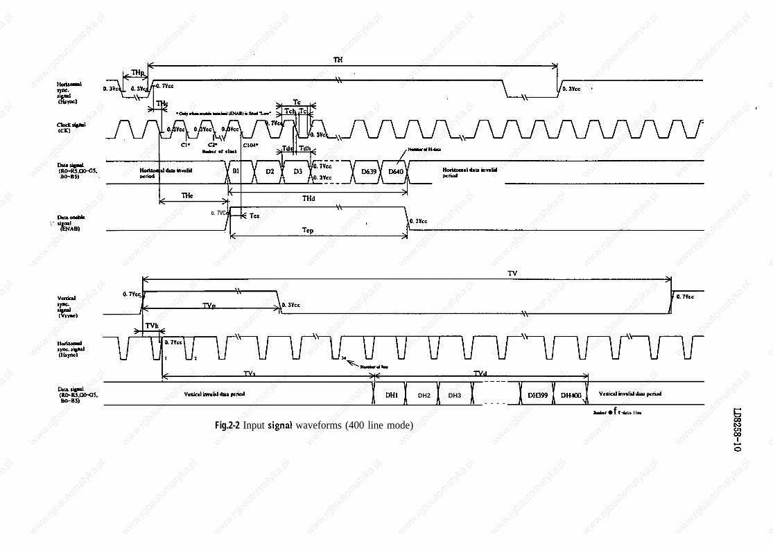
7. Tning Characteristics of input signals
Timing diagrams of input signal are sho~vn in Fig.2- 1-3.
.1. Timing characteristics
Paran
clock
Data
Horizontal
s?mc. signal
Vertical
s}nc. signal
eter
Hieh time
Lotv time
Setup time
Hold time
Cycle
Pulse \vidth
Cycle
Pulse ~vidth
Sjmbol Mode Min. T}T. Max. Unit
lfrc all – 25.18 28.33 MHz
Tch 11 5 — — ns
Tcl 11 10 – –ns
Tds 11 5 – – ns
Tdh 11 10 – – ns
TH 11 30.00 31.78 – ,ffS
// 750 8U0 900” clock
THp i] 2 96 200 clock
T v 480 515 525 560 line
400 446 449 480 line
350 447 449 510 line
Tvp all 1 – 34 line
Horizontal display period THd 11 640 640 640 clock
Hs?nc-Clock THc ~j 10 –Tc-10 ns
tIhase difference I l l I l lH~nc-Vqmc I Tvh //
Io– TH-THp clock
phase difference I
Remark—
—
.
—
—
—
Note) In case of Io\ver frequenq, the deterioration of display quali~, flicker etc.,may be occurred.
7-2. Horizontal display position
The horizontal display position is determined by ENAB signal and the input data corresponding
to the rising edge of ENAB signal is displayed at the lett end of the active area,
Parameter s~mbol Min. TIT. Max. Unit Remark
Enable signal Se(up time Tes 5 – Tc- 10 ns –
Pulse ~vidth Tcp 2 640 640 clock —
Hs:nc-Enable signal THe 44 – 164 clock —
phase difference
Note) When ENAB is fixed “LoJv”, the display starts from the data of C 104(clock) as shotvn
in Fig.2- 1-3. Be careful that the module does @ \vork ~vhen ENAB is fixed “High”.
7-3, Vertical display position
The vertical display position is automatically centered in the active area at each mode
of VGA,480-,400-, and 350-line mode. Each mode is selected depending on the polarity of
the s}mchronous signals described in 4-1 (Note 1 ).

LD8258-8
In each mode, the data of TVn is displayed at the top line of the active area. And the
display position \vill be centered on the screen like the follolving figure \vhen the period of
vertical synchronous signal,TV,is ~~ical value.
In 400-, and 350-line mode,thc data in the vertical data invalid period is also displayed.
So,inputting all data “O” is rec~mmended during vertical data invalid period.
ENAB siyal has no relation to the vertical display position.
mode v-data Startws) Vdab @odmd) V*IW sm~n) V+lw w“d Utit Remarii480 34 480 34 480 h –
400 34 400 443-TV 480 line –
350 61 350 445-TV 480 line –
h 181vd
~1 =1
-40em9 * Invtidx -ask
~ @~ 400 UIIUd- ~ed
3soon0
AI Im.dd peliod _40nln d- lnv~d p-iOd 85UCN
4001 ines mode (TV+49) ‘ 3501 ines mode (TV+49)
7-4. Input Data Signals and Display Position on the screen
Display position of input data (480 lines mode)
!
UP
\
D1, DH1 D2,DH1 D3,DH1 D640,DH 1
D1,DH2 D2,DH2
D1,DH3
m21, DH480
I
/
R/L=H
UID=L

\.-d V& IDM
Fig 2-1 Input signal waveforms (480 line mode)
.-
sF-Mgd(Vs?nc)
‘lHe k ATHd
o. 7VC
. . 1
I 1 1---- 1
mm e(:gptiGo-G5. Vmical inniill h pcti DH1 DH2 DH3
Ivenial hnlii &a pclilnl
- - - -*r ● f V*I. Ii”
Fig.2-2 Input signal waveforms (400 line mode)
,

TH
0. WCC
TvF 2
.1 m. \\ I
-’n” “’ ‘“- ‘;
Fig.2-3 Input signal waveforms (350 line mode)

LD8258-12
8. hl[
Colors &
;ray scale
Black
Blue
Green
cyanRed .
Magenta
Yellow
White
Black
a
Darker
u
Q
Brighter
oRed
Black
uDarker
o
QBrighter
o
Green
Black
oDarker
u
8
Brighter
“oBlue
ut Signals, Basic Display Colors and Gray Scale of Each Color
Data signal
Gray Scale RO R1 R2 R3 R4 R5 GO G1 G2 G3 G4 G5 BO B1 B2 B3 B4 B5
— 0 0 0 0 0 0 0 0 0 0 0 0 0 0 0 0 0 0— 000000 0 0 0 0 0 0 111111— 000000 111111 000000
000000 111111 111111— 111111 0 0 0 0 0 0 000000— 1 1 1 1 1 1 0 0 0 0 0 0 1 1 1 1 1 1— 1 1 1 1 1 1 1 1 1 1 1 1 000000— 1 1 1 1 1 1 1 1 1 1 1 1 111111
GSO 0 0 0 0 0 0 0 0 0 0 0 0 0 0 0 0 0 0
GS1 100000 000000 000000
GS2 0 1 0 0 0 0 0 0 0 0 0 0 0 0 0 0 0 0
+ + 4 +
+ + + +
GS61 101111 0 0 0 0 0 0 0 0 0 0 0 0
GS62 011111 0 0 0 0 0 0 000000
GS63 111111 0 0 0 0 0 0 000000
GSO 0 0 0 0 0 0 0 0 0 0 0 0 000000
GS1 0 0 0 0 .0 0 1 0 0 0 0 0 000000
GS2 0 0 0 0 0 0 0 1 0 0 0 0 000000
+ + + 4
4 + + +
GS61 0 0 0 0 0 0 1 0 1 1 1 1 000000
GS62 0 0 0 0 0 0 0 1 1 1 1 1 0 0 0 0 0 0
GS63 000000 1 1 1 1 1 1 000000
GSO 000000 0 0.0 0 0 0 000000
GS 1 000000 0 0 0 0 0 0 100000
GS2 000000 000000 010000
+ + + +
+ + + +
GS61 0 0 0 0 0 0 0 0 0 0 0 0 101111
CS62 0 0 0 0 0 0 0 0 0 0 0 0 011111
GS63 0 0 0 0 0 0 0 0 0 0 0 0 111111
O:Low level voltage, l. :High level voltage
Each basic color can redisplayed in64grayscdes fiom6bit data sign~s. According to t}lecombination oftotd 18 bit data
signals, the 262, 144-color display cm be achieved on the screen.

LD8258-13
9. Optical Characteristics
Ta=25°C. VCC=+5V.- —- —, --- -.
Parameter S}mbol Condition Min. T}p. Max. Unit Remark
Vie{ving Horizontal 021 (CR>5) (60) – –Deg. [Note] ,4]
angle e 22 (60) – – Deg.
range Vertical 011 (+(~9 - - Deg.
012 (m)~~ ) – – Deg.
Contrast ratio CR Best vietving 100 – – – [Note2,4 ]
angle
Response Rise rr 0 =0” – 30 –ms [Note3,4 ]
lime Decay rd — 50 – ms
;hromatici@ of x — 0.313 – – [Note4 ]
vhite Y — 0.329 – –
Luminance of \vhite YL TED (300) – cd/m2
White Uniformi~ 6 Iv — — 1.45 – [Notej ]
XThe measurement shall be executed 30 minutes after lighting at rating. (~~ical condition:lL=TBDmArms)
The optical characteristics shall be measured in a dark room or equivalent state \vith the method
sho~~m in Fig.3 belo~v.
Photodetector (BM-5A: TOPCON)
I
I,
1!1
/I
Field=2° c;>II1I
TFT– LCD moduleI
itI \I
\
4 0 0 m m
L C D panel
f,
1 —-— .—. — -—-— & —-—-—-—-— -—-—- JII*
I
Center of the screen
Fig. 3 Optical characteristics measurement method

LD8258-14
[Notel ] ~fmitions of viewing angle range:
Normal l i n e
022
012
--
/6 o’clock direction
[Note2] Definition of contrast ratio:
The contrast ratio is defined as the following.
Luminance (brightness) with all pixels whiteContrast Ratio (CR) =
‘ Luminance @rightness) with all pixels black
[Notes] Definition of response time:
- The response time is defined as the following figure and shall be measured by
switching the input signaI for “black” and “white”.
—>time
[Note4] This shall be measured at center of the screen.
[Note5] Definition of white uniformity:
White uniformity is defined as the
following with five measurements
(A-E).
120
240
360pixel
(5 w=Maximum Luminance of five points (brightness)
Minimum Luminance of five points (brightness)

10. Display Quantity
~D’
LD8258-15
11. Handling Precautions
a) Be sure to turn off the power supply when inserting or disconnecting the cable.
b) Be sure to design the cabinet so that the module can be installed without any extra stress such as
warp or twist.
. c) Since the front polarizer is easily damaged, pay attention not to scratch it.
d) Wipe off water drop immediately. Long contact with water may cause discoloration or spots.
e) When the panel surface is soiled, wipe it with absorbent cotton or other soft cloth.
0 Since the panel is made of glass, it may break or crack if dropped or bumped on Ilard surface.
Handle with care.
g) Since CMOS LS1 is used in this module, take care of static electricity and injure the human earth
when handling.
h) Observe all other precautionary requirements in handling components.
i) This module has its circuitry PCBS on the rear side and should be carefully handled in order not
to be stressed.
j) Laminated film is attached to the module surface to prevent it from being scratched . Peel the
film off sIowIy, just before the use. witi strict attention to electrostatic ch~ges. Ionized air sh~l
be blown over during the action. Blow off ‘dust’ on the polarizer by using an ionized nitrogen gun,
etc.
12. Packing form
a) Piling number of cartons : MAX. TBD
b) Package quantity in one carton: TBD
c) Carton size: TBD(W) X TBD(D) X TBD(H)rnm
d) Total mass of 1 carton filled with full modules : TBD g

I 4. L\wllaul&*by swab 1.-U.*
No. ‘ Test item Conditions
1 High temperature storage test Ta=60~ 2 4 0 h
2 Low temperature storage test Ta=-25~ 240h
3 High temperature Ta=40~ : 95%RH 240h
& high humidity operation test (No condensation)
4 High temperature operation test Ta=50”C 2 4 0 h
5 Low temperature operation test Ta=O~ 240h
6 Vibration test Frequency : 10~57Hflibration width (one side) :O.075mm
(non- operating) : 58-500H~Gravity:9 .8m/sZ
Sweep time :11 minutes
Test period :3 hours
(1 hour for each direction of X,Y,Z)
7 Shock test Max. gravity: 490m/sZ
(non- operating) Pulse width: 11 ms, half sine wave
Direction: AX,&Y,AZ
once for each direction.
[Result Evaluation Criteria]
Under the display quality test conditions with normal operation state, these shall be no change
which may affect practical display function.
14. Others
1) Lot No. Label:SMRP
+
Model No.LQ1OD42
52 3W4 Lot No.WE IN JMM
2) Adjusting volume have been set optimally before shipment, so do not change any adjusted value.
If adjusted value is changed, the specification may not be satisfied.
3) Disassembling the module can cause permanent damage and should be strictly avoided.
4) Please be careful since image retention may occur when a fixed pattern is displayed for a long
time.
5) If any problem occurs in relation to the description of this specification , it shall be resolved
through discussion with spirit of ~ooperation.
I
,,;I
I
II
I

m
o mv
mclJcQm-k
6060 I+I+l+l+lwoooo-
wm
z0—F—
In0a
><-1mW
?-1wNwm
.,. .mNmmu. . . . ,. ., wqmuoa
4Z z z z0 0 0 0 >——. . <+Ft-1--lUuuumWwll.lwmuciuu —— — — .00 0 0 0IllluXx>>o
<.. —-.n
/ ‘./ . -1
\.0 j \—u-l ‘N I’m“ I
IJ
I\-\\\\\ 9 “E’
\‘. -----
wuz<aUJ
-1Dt -
0w
L
uwL
Wwuw>Uuuukzzzz–<<<<3IYCKIYUO
3,
,. ------ Wwwww– mm-1-l -l_l_J Wzoooom *3t-l-l- t-o ox~ z
:w
R0w
3:z?0
\
.--— -
rwauv 2A IL3V)Z ‘6L
u)zo—(n
zwEwo
LIJz—-Jt-30
(’Jd00v
a-J
.w—LL
—
.r
c..
<
.
1
1
\
[
1
I1,.--. .— –,
,lf9Nl N3d0 1 3 2 3 9 ) 2 “18!!- 1~” I
_-— —_.— - —-1! -—w LL-—-———— ——
4
uc
1 I
1
1
,
\
/“I1 ’. .
(16)
,Z91
I Iu
—rlT4m
0d 1
I I N