Embed Size (px)
Citation preview

Editorial-Chief
Hideyuki Ichiyama Editorial Advisors
Hisao Takahashi Omi Kuriwaki Daisuke Kashibuchi Masayuki Sato Hiroaki Sakai Takahiro Otsuka Tetsuo Kojima Makoto Sato Takao Ikai Kunihiko Egawa Mineo Okada Keita Urayama Eunjin Choi Kazuki Yamanaka Ryo Ikehara Toshihiro Kurita
Vol. 172 Feature Articles Editor
Toru Matsuoka Editorial Inquiries
Hideyuki Ichiyama Corporate Productivity Engineering & Logistics Dept. Fax: +81-3-3218-2465
Mitsubishi Electric Advance is published on line quarterly (in March, June, September, and December) by Mitsubishi Electric Corporation. Copyright © 2020 by Mitsubishi Electric Corporation; all rights reserved. Printed in Japan.
The company names and product names described herein are the trademarks or registered trademarks of the respective companies.
CONTENTS
Technical Reports
Overview .......................................................................................... 1 by Yukio Yasuda Development of SiC-MOSFET Chip Technology .......................... 2 by Masayuki Imaizumi Development of Wiring Technologies to Improve Power Module Performance .................................................................................... 5 by Yoshihisa Uchida and Arata Iizuka 2000 V Class IGBT Concept for Renewable Energy Converter .. 9 by Satoshi Miyahara and Masaomi Miyazawa Humidity Robustness Verification Test for HVIGBT Modules .. 13 by Kenji Hatori and Keiichi Nakamura Development of Surface-mount IPM ........................................... 17 by Shuhei Yokoyama and Shogo Shibata
Mitsubishi Electric
Dec. 2020 / Vol. 172
Power Devices
Precis
Mitsubishi Electric’s power modules, which employ the latest chip and package technology, realize ideal power electronics systems thanks to their high quality, low loss, and excellent noise performance.

*Senior General Manager, Power Device Works Mitsubishi Electric ADVANCE December 2020 1
TECHNICAL REPORTS
Overview
Author: Yukio Yasuda*
Latest Technology Trends and Prospects for Power Modules
The increasing consumption of energy and the emission of massive quantities of CO2 are global issues that must be urgently addressed.
Currently, approximately 40% of the primary energy consumed around the world is used to generate electricity, and the ratio is estimated to exceed 50% within the next 25 years. Power electronics are crucial for solving such problems, and power devices are key components that need to be progressed.
The structure of IGBTs that use Si as a semiconductor material has advanced, from the planar gate structure to the trench gate structure and our proprietary CSTBT structure. In addition, the characteristics have been improved by using ultrathin wafer processing and back patterning technologies.
The performance of power devices is not determined only by the chips; packaging technologies that make the most of the characteristics of the chips are also important. In addition to conventional technologies, we have various new technologies such as resin insulation, molding, and low inductance wiring technologies. Moreover, various other technologies, such as on-chip sensing technologies to detect chip temperature and protection technologies (e.g., intelligent power modules (IPM)), can be combined at the user’s request.
These technologies allow us to provide small, light-weight, high-efficiency (low-loss), high-robustness, and high-reliability devices for a wide variety of sectors such as home appliances, industry, automobiles, electric railway, and power transmission.
In the power electronics sector, SiC as WBG semiconductors in particular has been gaining attention as a material that may replace Si due to its excellent physical properties. Mitsubishi Electric Corporation started developing SiC semiconductors ahead of other companies and succeeded in commercializing cutting-edge SiC power modules for various applications as a pioneer in the industry, and has been improved them further.
Mitsubishi Electric provides power modules with capacities ranging from 100 W to several MW for various applications. These modules incorporate leading-edge technologies to help reduce the global consumption of energy.
*Power Device Works 2
TECHNICAL REPORTS
Development of SiC-MOSFET Chip Technology
Author: Masayuki Imaizumi*
1. Introduction
Power devices that make it possible to use electric energy efficiently are equipped with semiconductor chips, such as transistors and diodes, which play a key role in current and voltage control. While Si semiconductor chips are mainly used at present, the application of wide band gap silicon carbide (SiC) semiconductors has begun to improve the performance and reduce the loss. Thanks to the excellent physical properties of SiC, SiC devices reduce the loss in power conversion by 50–70% and can function at higher frequencies than the conventional types. Using SiC devices based on the characteristics of systems can reduce the power loss of equipment and allow coolers and passive components to be made smaller.
To spread the use of SiC power devices that save both energy and resources, Mitsubishi Electric Corporation has been continuously working to improve their performance and reduce the costs. This report summarizes the latest development of SiC chips.
2. SiC Chip Development
2.1 Second-generation planar MOSFETs
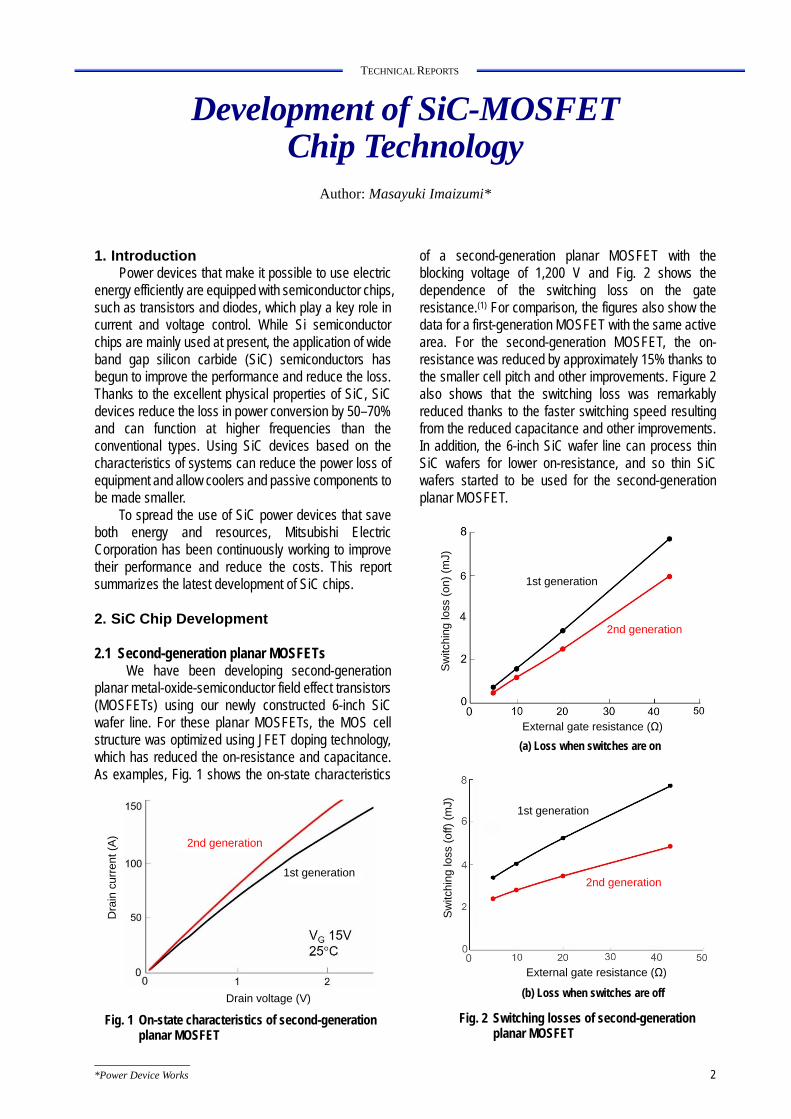
We have been developing second-generation planar metal-oxide-semiconductor field effect transistors (MOSFETs) using our newly constructed 6-inch SiC wafer line. For these planar MOSFETs, the MOS cell structure was optimized using JFET doping technology, which has reduced the on-resistance and capacitance. As examples, Fig. 1 shows the on-state characteristics
of a second-generation planar MOSFET with the blocking voltage of 1,200 V and Fig. 2 shows the dependence of the switching loss on the gate resistance.(1) For comparison, the figures also show the data for a first-generation MOSFET with the same active area. For the second-generation MOSFET, the on-resistance was reduced by approximately 15% thanks to the smaller cell pitch and other improvements. Figure 2 also shows that the switching loss was remarkably reduced thanks to the faster switching speed resulting from the reduced capacitance and other improvements. In addition, the 6-inch SiC wafer line can process thin SiC wafers for lower on-resistance, and so thin SiC wafers started to be used for the second-generation planar MOSFET.
Fig. 1 On-state characteristics of second-generation planar MOSFET
Dra
in c
urre
nt (
A)
Drain voltage (V)
1st generation
2nd generation
Fig. 2 Switching losses of second-generation planar MOSFET
1st generation
2nd generation
External gate resistance (Ω)
Sw
itchi
ng lo
ss (
off)
(m
J)
(b) Loss when switches are off
External gate resistance (Ω)
2nd generation
1st generation 1st generation
2nd generation
Sw
itchi
ng lo
ss (
on)
(mJ)
(a) Loss when switches are on

Mitsubishi Electric ADVANCE December 2020 3
TECHNICAL REPORTS
Currently, we have been developing various types of second-generation planar MOSFETs with the blocking voltage ranging from 600 V to 3.3 kV, and have been successively applying them to power modules for commercialization.
2.2 Trench MOSFETs with new structure
We have been developing trench MOSFETs with our proprietary structure for SiC power modules.(2) Due to the physical properties of SiC, the electric field intensity in SiC chips unavoidably tends to increase; in particular, the intensity of the electric field to be applied to the gate oxide at the trench bottom becomes high. Therefore, SiC-MOSFETs require special consideration, unlike Si trench MOSFETs. Figure 3 illustrates the structure of a trench MOSFET that we have been developing. To weaken the electric field to be applied to the gate oxide at the trench bottom, a bottom p-well (BPW) is provided at the lower section of the trench. To stabilize the electric potential of this BPW, ion implantation of p-type dopants is performed diagonally to the trench sidewall for electric connection. For the
section at the trench sidewall where currents pass, angled ion implantation of n-type dopants is performed to reduce the electric resistance. Figure 4 shows the on-resistance of a prototype trench MOSFET at room temperature. Figure 5 shows the blocking voltage characteristics. Compared to our planar MOSFET, the specific on-resistance of the trench MOSFET is approximately 50% lower at 1.84 mΩcm2. The avalanche breakdown voltage is 1,560 V as designed.
Such low resistance characteristic of trench MOSFETs will be used in the future to downsize chips in order to reduce the cost and increase the rated current of modules.
2.3 SBD-embedded MOSFETs
MOSFETs have pn diodes (body diodes) that enable the current to flow in the reverse direction thanks to their structure and they may be used as commutation diodes. However, with existing SiC-MOSFETs, when the body diodes are used, the on-state voltage sometimes increases. For MOSFETs with a large area and high blocking voltage, in particular, the SBDs as commutation diodes need to be connected in a row or screening testing of the body diodes is required to avoid the increase in on-state voltage.
For MOSFETs with the blocking voltage of 3.3 kV or higher, we have been developing SBD-embedded MOSFETs for which SBDs are built in the unit cells of the MOSFETs and that eliminate the need for SBDs as commutation diodes and screening test of the body diodes.(3) When a current flows in the reverse direction through the SBD built into an SBD-embedded MOSFET, the voltage to be applied to the pn junction of the body diode is reduced due to the voltage drop caused by the current flowing in the drift layer and thus no current is induced on the body diode.
Figure 6 shows the on-state characteristics of a prototype SBD-embedded MOSFET. The on-state characteristics are similar to those of a normal MOSFET
Fig. 3 Schematic cross-sectional structure of trench MOSFET
Fig. 4 Comparison of on-state resistance between planar and trench MOSFET
On-
resi
stan
ce (
mΩ
cm2 )
Planar type Trench type
Fig. 5 Off-state characteristics of trench MOSFET
Drain voltage (V)
Dra
in le
ak c
urre
nt (μ
A)

4
TECHNICAL REPORTS
that can be controlled by gate voltage. Since the area of the electrodes of the built-in SBD can be made small, the increase in the specific on-resistance is small. Figure 7 shows the reverse current conduction characteristics of an SBD-embedded MOSFET when the MOSFET gate is off (VG -5V) and on (VG 15V). The figure shows that when the voltage is approximately 1 V (diffusion voltage of the SBD), a current starts flowing and the unipolar current flows linearly. When the MOSFET gate is set to on, the current flowing on the MOSFET channel is superposed on the SBD current, greatly reducing the resistance.
By applying SBD-embedded MOSFETs to modules it is possible to omit SBDs, which are used to be connected in a row, and to simplify testing, thus downsizing the modules and reducing the costs.
3. Conclusion
We will continue developing second-generation planar MOSFETs, trench MOSFETs, and SBD-embedded MOSFETs to further improve the performance of power devices. We intend to help save energy and resources in various systems by utilizing the characteristics of SiC.
References (1) T. Tanioka., et al.: High Performance 4H-SiC
MOSFETs with Optimum Design of Active Cell and Re-oxidation Process, PCIM Europe, 879–884 (2018)
(2) Y. Fukui., et al.: Effects of Grounding Bottom Oxide Protection Layer in Trench-Gate SiC-MOSFET by Tilted Al Implantation, ICSCRM, Mo-1A-02 (2019)
(3) S. Hino., et al.: Demonstration of SiC-MOSFET Embedding Schottky Barrier Diode for Inactivation of Parasitic Body Diode, Mat. Sci. Forum, 897, 477–482 (2017)
Fig. 7 Reverse current conduction characteristics of SBD-embedded MOSFET
Drain voltage VDS (V)
Dra
in c
urre
nt d
ensi
ty ID
S (
A/c
m2 )
Fig. 6 On-state characteristics of SBD-embedded MOSFET
Drain voltage VDS (V)
Dra
in c
urre
nt d
ensi
ty I D
S (
A/c
m2 )

* Power Device Works Mitsubishi Electric ADVANCE December 2020 5
TECHNICAL REPORTS
Development of Wiring Technologies to Improve Power Module Performance
Authors: Yoshihisa Uchida* and Arata Iizuka*
1. Introduction
In the power electronics industry, to save energy and protect the environment, power modules are being widely used in home appliances, industrial equipment, automobiles, and railway application. There are needs to improve the performance of power modules, including downsizing, higher current density, and longer lifetime, depending on each application. To satisfy such needs, it is important to develop internal wiring technologies.
Table 1 lists the typical internal wiring technologies used for power modules. Previously, wire bonding using Al wires was commonly used. To improve the current density and lifetime, Al alloy wires and Cu wires have been applying. In addition, the use of the direct lead bonding (DLB) structure, in which main terminals are directly soldered on the chips, has been also applying. This report describes packaging technologies, focusing on these internal wiring technologies.
2. Wire Bonding
A general internal wiring technology for power modules is wire bonding with a diameter of 200–500 μm of Al by ultrasonic wedge bonding. This technology provides a higher flexibility in wiring. On the other hand, the lifetime of the products is often determined by the lift-off lifetime of the bonded wires. Lift-off is the phenomenon in which a crack develops at the bonded-junction of a wire due to stress caused by a difference in the coefficients of thermal expansion (CTE) between the wire and chip and the wire eventually remove from the chip. Mitsubishi Electric Corporation has been studying ways of solving such problems by optimizing the module structure and using new wire materials.
2.1 Al alloy wire Al alloy wires, which are developed by adding trace
quantities of different kinds of metal to Al wires to strengthen the wire material, improve the lift-off lifetime.(1)
Figure 1(a) shows the comparison results of the degradation rate of shear strength of samples in which the conventional type of AI wire and the new type of Al alloy wire were wire bonded on AI and enhanced electrode after a temperature cycling test (50 to 150C). If an Al alloy wire is applied to the conventional Al metallization (Sample B), the degradation rate of shear strength is not further improved than AI wire bonded to conventional Al metallization (Sample A). However, when an enhanced electrode is combined with an Al alloy wire, the degradation rate of the bonded junction of the wire is substantially improved (Sample C). Cross-sectional images at the bonded junction of each Sample after the temperature cycling test are shown in Fig. 1(b). Al alloy wire bonded to a conventional Al electrode (Sample B) shows the crack is selectively propagated into Al electrode where is concentrated of strain.
Meanwhile, in Al alloy wire bonded to an enhanced electrode (Sample C), the crack is propagated into the wire. From the results, applying Al-alloy wire which has high mechanical strength in combination with enhanced electrode can contribute to improve the lift-off lifetime on wire bonding junction.
2.2 Cu wire
Since the recrystallization temperature of Cu wires is higher and the CTE mismatch between wire and chip is less than Al wires, the lift-off lifetime is expected to be much longer.(1) To confirm the improvement of lift-off
Table 1 Types of wiring technology

6
TECHNICAL REPORTS
lifetime, the power cycling lifetime of Al and Cu wire bonded samples are compared. Figure 2 shows the appearance of a sample with Cu wires bonded and the power cycling test results. The lift-off lifetime of the sample with Cu wires bonded is approximately 35 times longer, which is the remarkable extension of lift-off lifetime. For this sample, to reduce a deterioration of the die attach junction, an Ag sintering material was applied.(2)
Cu wires are harder than Al wires and are required larger energy for bonding. Various structures have been proposed to prevent chips from breaking when the wires are bonded. For example, chip electrodes are plated with a thick layer and a buffer plate is installed on top of an electrode.(3) To take advantage of superior property of Cu wire, it is not enough to apply Cu wire, but needs to optimize a package structure.
3. Direct Lead Bonding (DLB) The DLB structure in which external terminals are
directly soldered onto chips eliminates any internal wires to connect to terminal. Therefore, the area required for such wires can be reduced, which helps downsize packages. In addition, DLB structure has advantageous for high power density because terminal can be bonded a larger junction area compared to wire bonding.
3.1 DLB for case type modules
In 2011, we released the J-series transfer-molded power module T-PM for automobiles, featuring the DLB structure and transfer molded structure. Due to expansion of the xEV market in recent years, there is more demand for smaller power modules with higher current density. To satisfy this need, we have developed case type modules (J1 series). In this product, a grease-
Fig. 1 Comparison of conventional Al wire and enhanced Al alloy wire
(a) Degradation of shear strength (b) Cross-sectional SEM image
Fig. 2 Results of power cycling test of Cu wire bonded sample

Mitsubishi Electric ADVANCE December 2020 7
TECHNICAL REPORTS
free structure with a built-in cooling fin was combined with the DLB structure. Figure 3 shows the appearance and cross-sectional structure of the J-series T-PM and J1 series. For the J1 series, our proprietary seventh-generation IGBT/diode was applied and the DLB technology was combined with direct potting (DP) resin encapsulation technology. This has made it possible to provide smaller high-power modules even for larger case
type modules by utilizing the advantages of the DLB structure. In addition, we released the high-power J1 series: the output capacity was approximately doubled while the increase in size was suppressed to only approximately 1.5 times by optimizing the internal wiring layout. Thus, we have been expanding line-up of this kind of products Figure 4 compares the high-power J1 series to the conventional type. The adopted DLB
Fig. 4 Improvement in characteristics of high-power J1 series
Fig. 3 Sample photo and cross-sectional diagram of DLB type modules

8
TECHNICAL REPORTS
structure, built-in fin and optimized internal wiring layout reduced the mounted area by 50%, weight by approximately 70%, and thermal resistance by 25% compared to the conventional transfer-mold type with the same output. In addition, optimization of the wiring layout reduced the self-inductance by 25% compared to the wire-bonding type.
In the DLB structure, the lifetime of soldered junctions is greatly affected by the solder shape. However, for large case type modules, the clearances between the chips and terminals tended to be unstable and it was difficult to control the solder shape. Meanwhile, providing a through hole at the soldered joints of terminals can stabilize the solder shape. This enables to applied DLB structure for large case type and to realize the longer lifetime which is feature of the DLB structure. We will apply the DLB technology used in case type modules to products in other applications to provide smaller but higher-power modules.
3.2 Direct power board bonding
We are developing the new structure shown in Fig. 5 by the improving DLB technology in which Cu leads used to be wired two-dimensionally. In the new structure, heavy-current power boards (multilayer circuit boards) are directly soldered onto the chips. The power board with multilayer wiring patterns above and below the insulating layer allows wiring in two layers (upper and lower), including signal wires by one board. This new structure allows further downsizing of modules and optimization of the electrical characteristics. The optimization of balancing currents and switching timing of each chips is become easier by 2 layers wiring design. Moreover, it has been confirmed that reduction in parasitic inductance by using mutual inductance between the upper and lower patterns.
Thus, by using power boards it is possible to make modules smaller, optimize the electrical characteristics, and cope effectively with complex topologies in the future.
4. Conclusion Mitsubishi Electric will continue developing wiring
technologies to increase the current density and lifetime to offer suitable products that satisfy market needs as follows; Wire bonding
Improving the lifetime by using new wiring materials with optimizing electrode structure to match new materials. Direct lead bonding (DLB)
Applying the DLB technology (for case type modules) to other types of products for downsizing and longer service life New wiring structure
Applying the DLB technology involving multiplayer circuit boards for downsizing, improving the characteristics, and coping with complex topologies
References (1) Uchida Y., et al.: Wiring technology for upcoming
generation power module, Proc. PCIM Europe, Nuremberg Germany (2020)
(2) Nakahara K., et al.: Development of Package Structure for High-Temperature Operation, Mitsubishi Electric ADVANCE, Vol. 165 (2019)
(3) Uchida Y., et al.: Investigation of Highly Reliable Structure with Cu Wire for Power Module, Proc. 24th Symposium on Microjoining and Assembly Technology in Electronic, Yokohama, Japan (2018)
Fig. 5 Sample photo and cross-sectional diagram of case type module using power board

*Power Device Works Mitsubishi Electric ADVANCE December 2020 9
TECHNICAL REPORTS
2000 V Class IGBT Concept for Renewable Energy Converter
Authors: Satoshi Miyahara* and Masaomi Miyazawa*
1. Introduction
It has been a long time since the 1500 Vdc rated photovoltaic converter acquired a large share of the market. The pressure to reduce costs continues to increase, as does the competition for CapEx savings. Led by the growth of the renewable energy market, there are growing expectations for the battery energy storage system (BESS) for a more sustainable distributed power network. In this market, the 1500 Vdc rated converters have started being installed in the field. Moreover, wind converters with high output voltages are being considered. The typical output voltage rating is 690 Vac or less, but a higher output voltage, e.g. 900 Vac, would bring the benefit of higher output power under the same output current. Such a highly rated wind converter has attracted much attention as a means of reducing system costs.
2. System Requirements
2.1 Operating DC voltage
To meet the requirements of the Low Voltage Directive, converter ratings must be lower than 1500 Vdc (or 1000 Vac).(1) Therefore, the highest Vcc is considered to be 1500 V. In reality, however, photovoltaic converters rarely see 1500 Vdc operation due to the panel output characteristics even if rated. Switching at a DC-link voltage of 1500 V with a small current at the start of operation (e.g., morning time) can occur, but voltages between 900 and 1300 V with a large current by maximum power point tracking (MPPT) control are typically expected. When the installed PV panel capacity is large, higher continuous voltages of up to 1400 V must be considered. Also, in grids with a high share of renewable energy, the energy feed-in PV power plant may be restricted, which increases the DC operating voltage. The BESS hardware design tends to be the same as that of the photovoltaic converter, but the operating voltage range is higher due to the difference in output characteristics between PV panels and Li-ion batteries. In a wind converter, on the other hand, a higher output current at 1500 Vdc can easily occur. The output power of a wind generator increases as the voltage increases. Therefore, in the case of a 900 Vac system, Vcc operation of around 1400 V should be considered. Even with the 690 Vac system, such a high Vcc operation
can occur when necessary to meet severe high-voltage ride-through (HVRT) requirements from the grid codes.(2) Therefore, the full SOA must be secured under the condition of Vcc = 1500 V. Also, a possible increase in the long-term DC stability (LTDS) failure rate caused by higher DC-link voltages should be taken into consideration.(3)
2.2 Solutions for 1500 Vdc operation
In the 1500 Vdc photovoltaic converter or BESS, the three-level neutral point clamped (NPC; I type) topology with a 1200 V or even a 950 V device is commonly adopted.(4) The LTDS failure rate is considered sufficiently low,(5) but the number of devices is three times that of the two-level topology and thus the system cost is higher, as is the control complexity and stray inductance. In some cases, a 1700 V device is used for the 1500 Vdc system although its robustness against LTDS failures and voltage spikes is lower than that of the NPC. Here, the idea of using a higher voltage rated device, e.g. 2000 V, would bring advantages over the above solutions, while retaining the benefits of the two-level topology: reliable switching performance, less complexity, and sufficient robustness against LTDS. Nevertheless, the design of the performance and reliability trade-off must suit the market requirements to a realistic degree. For example, zero LTDS failure with a much higher power loss by choosing a far greater voltage class device, such as a 2500 V, would reduce the efficiency of the converter.
3. Performance Evaluation
Considering the above system requirements, the higher voltage class IGBT and diode with a 2000 V rating were fabricated and the characteristics were tested.
3.1 LTDS
The LTDS of a semiconductor device depends on the applied voltage, temperature, and altitude.(5) In addition, the fundamental device technology, e.g. the structural parameters, also affects the robustness. For the 2000 V rated device, the 7th generation IGBT and diode technology are on a design basis, and a sufficient LTDS design is intended for each target application. The N-drift thickness and resistivity are the key parameters for determining the design of not only the blocking

10
TECHNICAL REPORTS
capability but also the LTDS.(6) Our 7th generation IGBT has a unique carrier stored trench-gate bipolar transistor (CSTBT™) structure, enabling a low conduction loss based on the optimal carrier density profile. The 7th generation diode has a relaxed field of cathode (RFC) structure on its cathode surface, which improves the power loss vs. snap-off behavior trade-off by utilizing the hole injection effect.(7) These unique technologies effectively compensate for the increase in power loss caused by the increase in thickness or resistivity.
Figure 1 shows the results of the accelerated LTDS test using an artificial neutron beam for a comparison between the existing device with a 1700 V rating and devices with a higher blocking voltage capability. The LTDS can be selectively designed to a certain degree using the increase in wafer resistivity because it reduces the electric field strength. In Fig. 1, the lines with gradient colors (2) illustrate the LTDS with different wafer resistivity and fixed thickness values. The lines are represented as statistically processed data based on the
actual test results, and thus the shape of the lines does not accurately represent the physical theory of cosmic ray induced failure. Although a higher resistivity improves the LTDS, the final design of the resistivity (and thickness) is carefully chosen taking into consideration other fundamental performances such as safe switching performance, power loss, etc.
3.2 Safe switching operation
The typical switching behavior of the 2000 V device was confirmed to maintain safe operation at Vcc = 1500 V. The test sample was chosen from the devices shown in Fig. 1, with a certain wafer thickness and resistivity that cover the LTDS requirements for the target applications. The current rating of the tested IGBT module was 400 A. Figure 2 shows the reverse-bias safety operating area (RBSOA) test waveforms. The IGBT turned off safely at the outermost boundary of the RBSOA (square area within the twice-rated current and rated blocking voltage of 2000 V) under the condition of
Fig. 2 RBSOA test waveforms at Tvj = 150°C
(b) Lissajous curve of collector current and collector-emitter voltage with RBSOA
(green dotted line)
(a) Time domain
Fig. 1 LTDS test results for differently tuned devices (a) IGBT (b) Diode

Mitsubishi Electric ADVANCE December 2020 11
TECHNICAL REPORTS
Vcc = 1500 V. The snap-off behavior of the diode was also
confirmed, as shown in Fig. 3. At Vcc = 1500 V with a low current, no snappy reverse recovery behavior was found. For the final product design, internally paralleled devices and stray inductance effects must be carefully considered.
3.3 Power loss performance
By increasing the blocking voltage of the device to 2000 V, the power loss (both conduction and switching) inevitably increased. However, due to the benefits of the CSTBT™ and RFC structure, the increase in the total power loss was within the minimum sacrifice while maintaining a sufficient LTDS performance. In particular, avoiding an increase in the switching loss is the most critical factor. In addition to the relatively higher switching frequency in the target application (1–3 kHz), the increase in the operating Vcc itself plays a large role in increasing the switching loss of both the IGBT and diode.
The above key factors were considered in the trial design of the 2000 V device, and the benefits of the power loss performance of the 2000 V device were investigated through a comparison with the existing 1700 V device and the “1500 Vdc enablers.” One option was the three-level NPC (I type) topology with a 1200 V device. A two-level topology with a 3300 V device was also included in the comparison as a standard voltage class higher than 1700 V, although the 3.3 kV device is much more suitable for traction applications where significantly higher DC-link voltages are required. The comparison was made under the same output power per mounting area. The output power for the 1700 V device was set for the 690 Vac system while it was set for the 900 Vac system for the others. Therefore, the output current for the 900 Vac system was smaller by the factor of the reciprocal of the output voltage ratio. The same package size and technology were assumed for the mounting area and the thermal resistance was assumed. The 1200, 1700, and 2000 V modules were considered as 1200 A rated, and the 3300 V module was considered as a smaller rated current due to its relatively larger chip area. In the three-level NPC topology with a 1200 V device, the usage of three dual IGBT modules with a 1200 A rating was assumed. Hence, the output power conditions were tripled to maintain the same output power per mounting area. (Table 1.)
The 2000 V device performance was comparable to the existing 1700 V device in the range of 0.5 to 3 kHz. (Fig. 4) This result indicates that the increased power loss (both conduction and switching) can be well compensated by possible output current derating thanks to the increased output voltage. Thus, significant system benefits can be obtained (e.g. reduction in ohmic losses in cables, reduction in windings of the grid connection
transformer, etc.) while keeping the same power feed-out to the grid. The other solutions for the 900 Vac bring the same advantages but with less output power. The 3300 V device technology is obviously too marginal for 1500 V operation. The performance of the three-level NPC topology with the 1200 V device was limited at lower switching frequencies by high conduction losses at
Fig. 3 Reverse recovery waveform at low current of 0, 10, 20 A at Vcc = 1500 V, Tvj = 25°C
Table 1 Conditions for power loss performance comparison
Fig. 4 Simulated junction temperature of the IGBT chip

12
TECHNICAL REPORTS
the output stage. Therefore, the performance was typically maximized at higher switching frequencies, but under the test conditions, the switching loss at the input stages again limited the performance.
Additionally, the output power performance at a fixed switching frequency of 2.5 kHz was compared (Fig. 5). The achievable output power per mounting area was very similar between the 2000 and 1700 V devices. However, considering the benefits of the reduced output current, the 2000 V device performed better, as shown under “Output power / mounting area @Tvj = 150°C / output current” in Table 2.
4. Conclusion
The new voltage class 2000 V rated IGBT module can meet the requirements based on recent converter designs for renewable energy applications. An increase in the operating Vcc and even system voltages from 690 to 900 V are feasible. The design boundary of the two-level converter is expanded with improved optimization including power loss performance, LTDS reliability, and converter system cost.
References (1) Low voltage directive, EU, 35 (2014) (2) H.G. Eckel., et al.: 690 V line side inverters with
improved reactive power capability for wind power integration, PCIM Europe, 1374–1382 (2013)
(3) N. Kaminski., et al.: Failure rates of IGBT modules due to cosmic rays, ABB Application Note 5SYA 2042_09.
(4) C.R. Müller., et al.: New 950V-IGBT and diode technology integrated in a low-inductive ANPC topology for applications, PCIM Europe, 160–167 (2019)
(5) U. Schilling., et al.: Cosmic Ray Failures in Power Electronics, Semikron Application Note AN17-003.
(6) K. Suzuki., et al.: Tight relationship among Field Failure Rate, Single Event Burn-out (SEB) and Cold Bias Stability (CBS) as a cosmic ray endurance for IGBT and diode, ISPSD, 184–187 (2018)
(7) M. Miyazawa., et al.: 7th generation IGBT Module for Industrial Applications, PCIM Europe, 34–38 (2014)
Table 2 Relative performance comparison
Fig. 5 IGBT chip temperature vs. output power per mounting area @ fc = 2.5 kHz

*Power Device Works Mitsubishi Electric ADVANCE December 2020 13
TECHNICAL REPORTS
Humidity Robustness Verification Test for HVIGBT Modules
Authors: Kenji Hatori* and Keiichi Nakamura*
1. Introduction
Railway transportation is more energy efficient than other means of transportation, and thus reduces the environmental impact of the entire transportation sector. Accordingly, the use of railways has been encouraged around the world to help mitigate global warming. In addition, to realize a low-carbon society, various measures have been promoted such as electrification of unelectrified railway sections and introduction of battery-powered railway vehicles. As a result, electric trains are now operating in various environments around the world.
Power modules for railway vehicles need to be small, low loss and highly reliable compared to those for consumer goods and general industries. Therefore, it is important to check the durability of such modules in various environments. Since modules are not hermetically sealed, it is difficult to completely eliminate the influence of humidity in highly humid environments, and so technologies for verifying robustness to humidity are strongly needed.
Under such circumstances, Mitsubishi Electric Corporation has been developing technologies for verifying the humidity robustness of HVIGBT modules. Using these technologies, we verified the effectiveness of a surface charge control (SCC) technology, which offers excellent humidity robustness, and developed our latest-generation X series of HVIGBT modules.
This report describes the humidity robustness verification technologies for HVIGBT modules that we have developed, along with verification results for the X series.
2. Mechanisms of Failures due to
Humidity
2.1 Known failure mechanisms The blocking voltage of power semiconductor chips
is retained by the terminations around their perimeter. Usually, aluminum electrodes are arranged in a ring shape at a termination and each ring bears part of the voltage. In one known failure mode, moisture ingress results in corrosion and failure of aluminum electrodes.(1) Another known failure mode is electrochemical migration (ECM) of copper, silver, and other metals.(1)
2.2 New failure mechanism
Through our studies on the humidity robustness of
power semiconductors, we found a new failure mode which may cause power semiconductors to fail, besides the aforementioned aluminum corrosion and ECM. The conventional aluminum corrosion and ECM take time to cause a failure. However, for the newly found failure mode, the leakage current starts increasing in several tens to several hundred seconds after starting to apply the voltage as shown in Fig. 1. This is not enough time for aluminum corrosion or ECM to proceed, confirming that the failure mechanism is a new one.(2)
This new failure mode can be confirmed as follows: An HVIGBT module is allowed to absorb moisture, then it is rapidly cooled to form condensation, then a DC voltage is applied. As shown in Fig. 1, when the module was dry, even after a DC voltage was applied, the leakage current of the device did not increase; on the other hand, when the module was in a state with condensation, the leakage current started increasing just 70 seconds after starting to apply the DC voltage. The results showed that although the device did not break, the increase in the leakage current while applying the DC voltage may have been caused by the blocking voltage performance becoming unstable.
Fig. 1 Condensation test
0.001
0.01
0.1
1
time [sec]
Leak
age
curr
ent
(mA
)
0.001
0.01
0.1
1
0 50 100 150 200time (sec)
1
0.1
0.01
0.0010 50 100 150 200
Time (sec)
50 100 150 200Time (sec)
1
0.1
0.01
0.001
Leak
age
curr
ent
(mA
)
(a) Voltage application in a dry state
(b) Voltage application in a state with condensation
The leakage current started increasing in 70 s.

14
TECHNICAL REPORTS
The mechanism by which a leakage current increases due to condensation is shown below. When a voltage is applied to a device, the gel (dielectric) polarizes along the electric field in the module; when the module absorbs moisture at the same time, the surface charge (+Qss) accumulates at the termination of the power semiconductor chip due to a combined effect with the gel polarization (Fig. 2).
Figure 3 shows the electric field distribution at the chip terminations when no surface charge (+Qss) exists and when surface charge (+Qss) has accumulated. In Fig. 3, the electric field is high in the green to red regions, and low in the blue region. The figure shows that when surface charge (+Qss) accumulates at a chip termination, the electric field at the chip termination becomes high. As a result, the blocking voltage of the device may decrease, which may increase the leakage current and
the device may break in the worst case.
3. Humidity Robustness Improvement Technology: Surface Charge Control (SCC)
For this newly found failure mode, Mitsubishi Electric developed the SCC technology(3) and released the X series of HVIGBT modules with higher humidity robustness. Figure 4 illustrates the conventional chip termination structure, and Fig. 5 illustrates the structure of the new chip termination with the SCC technology. In the conventional structure, the chip termination is covered with an insulated layer, while in the termination structure with the SCC technology, it is covered with a semi-insulated layer.
In the conventional structure, since the chip termination is covered with an insulated layer, there is no route to release the accumulated surface charge (+Qss). On the other hand, in the termination structure with the SCC technology, since the surface charge (+Qss) is released through the semi-insulated layer, the surface charge does not adversely affect the electric field at the chip termination. Therefore, the excellent blocking voltage property can be retained even when there is condensation.
Figure 6 shows the effect of the SCC technology that was verified in the aforementioned voltage application test with condensation. Figure 6 shows that even when the chip structure was the same, the leakage current increased in one cycle without the SCC technology, whereas for the structure with the SCC technology, the leakage current did not increase even in
Fig. 2 Gel polarization due to condensation
Gel polarization
Surface charge (+Qss) accumulation
Fig. 2 Gel polarization due to condensation
Fig. 3 Electric field inside the module in a state with condensation
No surface charge (+Qss) (in a dry state)
The electric field at the chip termination becomes high.
Surface charge accumulated (in a state with condensation)
Fig. 4 The conventional chip termination: covered by an insulated layer
Fig. 5 The new termination with SCC technology:covered by a semi-insulated layer
Mitsubishi Electric ADVANCE December 2020 15
TECHNICAL REPORTS
seven cycles.
4. Condensation Resistance Check Tests (Condensation Cycle Tests)
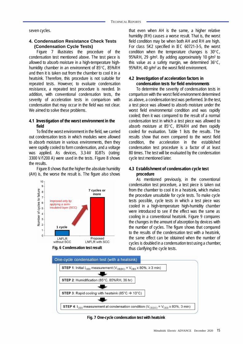
Figure 7 illustrates the procedure of the condensation test mentioned above. The test piece is allowed to absorb moisture in a high-temperature high-humidity chamber in an environment of 85C, 85%RH and then it is taken out from the chamber to cool it in a heatsink. Therefore, this procedure is not suitable for repeated tests. However, to evaluate condensation resistance, a repeated test procedure is needed. In addition, with conventional condensation tests, the severity of acceleration tests in comparison with condensation that may occur in the field was not clear. We aimed to solve these problems.
4.1 Investigation of the worst environment in the
field To find the worst environment in the field, we carried
out condensation tests in which modules were allowed to absorb moisture in various environments, then they were rapidly cooled to form condensation, and a voltage was applied. As devices, 3.3-kV IGBTs (rating: 3300 V/1200 A) were used in the tests. Figure 8 shows the results.
Figure 8 shows that the higher the absolute humidity (AH) is, the worse the result is. The figure also shows
that even when AH is the same, a higher relative humidity (RH) causes a worse result. That is, the worst field condition may be when both AH and RH are high. For class 5K2 specified in IEC 60721-3-5, the worst condition when the temperature changes is 30C, 95%RH, 29 g/m3. By adding approximately 10 g/m3 to this value as a safety margin, we determined 36C, 95%RH, 40 g/m3 as the worst field environment.
4.2 Investigation of acceleration factors in
condensation tests for field environments To determine the severity of condensation tests in
comparison with the worst field environment determined as above, a condensation test was performed. In the test, a test piece was allowed to absorb moisture under the worst field environmental condition and was rapidly cooled; then it was compared to the result of a normal condensation test in which a test piece was allowed to absorb moisture at 85C, 85%RH and then rapidly cooled for evaluation. Table 1 lists the results. The results show that even compared to the worst field condition, the acceleration in the established condensation test procedure is a factor of at least 80 times. The test will be evaluated by the condensation cycle test mentioned later.
4.3 Establishment of condensation cycle test
procedure As mentioned previously, in the conventional
condensation test procedure, a test piece is taken out from the chamber to cool it in a heatsink, which makes the procedure unsuitable for cycle tests. To make cycle tests possible, cycle tests in which a test piece was cooled in a high-temperature high-humidity chamber were introduced to see if the effect was the same as cooling in a conventional heatsink. Figure 9 compares the changes in the amount of absorption by devices with the number of cycles. The figure shows that compared to the results of the condensation test with a heatsink, the same effect can be obtained when the number of cycles is doubled in a condensation test using a chamber, thus clarifying the cycle tests. Fig. 6 Condensation test result
Improved only by applying a semi-insulated layer (SCC)
1 cycle
7 cycles or more
Fig. 7 One-cycle condensation test with heatsink

16
TECHNICAL REPORTS
4.4 Condensation cycle test results for the X series As described previously, the SCC technology with
excellent humidity robustness was applied to the X series. Table 2 shows the evaluation results of the X series in a condensation cycle test. The results show that the condensation resistance of the X series is at least 100 times that of the conventional device. When the aforementioned acceleration factor is considered, this result corresponds to condensation of 8,000 times in an environment equivalent to the worst field environment.
Table 2 Cycling condensation test result of X series
HVIGBT module
Conventional device (3300 V/1200 A)
Failure in 1 cycle
X series device (3300 V/1800 A)
No failure after 100 cycles
5. Conclusion We found a new mode of failure mechanism due to
humidity caused by the accumulation of surface charges and confirmed the effectiveness of the SCC technology, which is used for the X series chips. In addition, we established a condensation test procedure that makes cycle tests possible and confirmed that the X series can withstand 100 cycles of condensation tests and 8,000 times of condensation in an environment equivalent to the worst field environment.
We will use the established humidity robustness evaluation and improvement technologies to enhance the reliability of power semiconductor modules, thus helping to create both a low-carbon society and affluent life.
References (1) Christian Zorn., et al.: Acceleration of Temperature
Humidity Bias (THB) Testing on IGBT Modules by High Bias Levels, IEEE (2015)
(2) N. Tanaka., et al.: Robust HVIGBT module design against high humidity, PCIM Europe (2015)
(3) S. Honda: High Voltage Device Edge Termination for Wide Temperature Range plus Humidity with Surface Charge Control (SCC) Technology, ISPSD (2016)
(4) K. Nakamura: The test method to confirm robustness against condensation, EPE (2019)
Table 1 Comparison of test results between field condition and accelerated test condition
Worst field environmental condition (Cooling from 36C, 95%RH)
Failure in 80 cycles
Condensation test condition (Cooling from 85C, 85%RH)
Failure in 1 cycle
Fig. 8 Condensation test results under various humidification conditions
Possible worst case in the field
Incr
ease
d d
evic
e w
eig
ht
Fig. 9 Vapor absorption trend
Condensation test with a heatsink (cycles)
Condensation test using a chamber (cycles)
Condensation test using a chamber
Condensation test with a heatsink
Double

*Advanced Technology R&D Center Mitsubishi Electric ADVANCE December 2020 17
TECHNICAL REPORTS
Development of Surface-mount IPM Authors: Shuhei Yokoyama* and Shogo Shibata*
This report introduces our surface-mount intelligent power modules (IPMs) developed for fan motors.
This product was developed focusing on both functions and shape to reduce the cost of boards for customers. Regarding functions, a new interlock function was added and many other protection functions were incorporated into the product, which made it possible to reduce the number of parts to be mounted onto a board. Regarding the shape, to assure wide insulation distance between reduces the cost for insulation treatment when boards are assembled. In addition, as is the case with the SLIMDIPTM series, GND terminals for P-side driving power supplies are provided on the control side, which simplified the wiring pattern on boards and enabled the boards to be made smaller. Thanks to these characteristics, the product reduces the total board cost including the assembly process.
1. Introduction
Recently, as global attention has turned to saving energy, inverter systems have spread in a wide variety of sectors and markets in order to save energy. In ordinary households, inverters were first applied to air conditioners, as these consume large amounts of electricity. Mitsubishi Electric Corporation was the first in the industry to commercialize DIPIPMTMs (transfer-mold type IPMs) for air conditioner compressors, and has been contributing inverterization of home appliances.
To save more energy, the application of inverters to fan motors in addition to compressors has been accelerating. However, the current rating of most DIPIPM models is 5 A or higher and so they are not suitable for fan motors that operate at low currents (allowable current: 1 Arms or lower). In addition, regarding boards for fan motors, surface-mount IPMs are often used to reduce the parts mounting cost and the size of boards and so through hole type DIPIPMs could not satisfy customer needs.
Accordingly, we developed low-power surface-mount IPMs for fan motors(1) (Fig. 1). This report describes the outline and characteristics of this IPM.
2. Outline of the surface-mount IPM
This section describes the structure and electrical characteristics of the newly developed surface-mount IPM.
2.1 Structure
A surface-mount IPM consists of power, power
supply, and control sections (Fig. 2). The power section applies our RC-IGBT in which an IGBT and a diode are integrated and has six such devices (chips) to form a three-phase AC output inverter circuit. The power supply section has three BSDs with current limiting resistance for bootstrap circuits in the module. Power can be supplied to the HVIC with only a single 15V power source as its structure. The control section consists of an HVIC that drives the upper-arm (P side) IGBTs and an LVIC that drives the lower-arm (N side) IGBTs. The HVIC contains IGBT driving, high-voltage level shift, and control power supply undervoltage protection (UV) circuits. The LVIC includes IGBT driving, control power supply undervoltage protection (UV), short-circuit current protection (SC), overtemperature protection (OT), and
Fig. 1 Outline view of surface-mount IPM
Fig. 1 Outline view of surface-mount IPM
Power supply section
Control section
Power section
Fig. 2 Circuit diagram

18
TECHNICAL REPORTS
analog temperature output (VOT) circuits, as well as the new interlock function.
2.2 Electrical characteristics
Figure 3 shows the loss performance of the surface-mount IPMs. The loss of SP2SK (current rating: 2A product) is 25% lower than that of SLIMDIP-S(2) when operating at a carrier frequency of 20 kHz and Io of 0.3 Arms. Thanks to this reduction, a large energy-saving effect is expected under low-current driving conditions required for 100W fan motors.
Table 1 lists the other characteristics (e.g., saturation voltage). The lower loss of this product was achieved mainly by improving the switching time comparing to the conventional SLIMDIP-S (e.g., the speed was improved by approximately 40% (Tc(on): 0.35 to 0.2 µs)).
3. Characteristics of surface-mount IPMs
Figure 4 illustrates a board when a general surface-mount IPM is used: the board size is larger due to reasons (1) and (2) below and the total board cost is high, even if the unit cost of a module is low. In addition, additional countermeasure (3) is required, which increases the cost in the assembly process. For this product, more protection functions are integrated regarding problem (1) and the package shape was well-designed regarding problems (2) and (3) to reduce the total board cost including the assembly process. (1) An external protection part is required in addition to
an IPM. (2) Wiring patterns need to be drawn complexly due to
a problem with terminal arrangement. (3) The insulation distances between the terminals are
not enough. An insulation agent needs to be applied for insulation.
3.1 Functions Table 2 lists the protection functions of commonly
used surface-mount IPMs with the same size as this product. Since low-priced controllers are often used for fan motors, the upper and lower arms tend to turn on at the same time, leading to short circuit current flow. Therefore, in this product, to prevent breakage due to a short-circuit in the upper and lower arms, a new interlock function, which existing DIPIPMs lack, was added. In addition, all protection functions required for modules for fan motors have integrated to reduce the number of protection parts on boards.
Figure 5 illustrates the operation of the newly installed interlock function. Without the interlock function, when both P-side input signal (PIN) and N-side input Fig. 3 Loss comparison with current products
(Conditions: Vcc = 300 V, Io = 0.3 Arms, P.F. = 0.8, fc = 20 kHz, three-phase sine wave output)
0
0.1
0.2
0.3
0.4
0.5
0.6
0.7
SLIMDIP-S SP2SK
Loss
on
one
chip
(W
)
Reduced by 25%
Table 1 Electrical characteristics of SP2SK Item Symbol
Minimumvalue
Standardvalue
Maximumvalue
Unit
IC=2A, Tj=25C - 2.30 3.10
IC=2A, Tj=125C - 2.60 3.55
FWD forward voltage drop VEC - 2.30 3.00 V
ton - 0.85 1.30
trr - 0.25 -
tc(on) - 0.20 0.50
toff - 0.90 1.60
tc(off) - 0.10 0.35
VD=15V, VIN=0V - - 4.20
VD=15V, VIN=5V - - 4.20
VD=VDB=15V, VIN=0V - - 0.10
VD=VDB=15V, VIN=5V - - 0.10
Short-circuit protection trip level VSC(ref) 0.455 0.480 0.505 V
UVDBt Trip level 8.0 - 12.0 V
UVDBr Reset level 8.0 - 12.0 V
UVDt Trip level 10.3 - 12.5 V
UVDr Reset level 10.8 - 13.0 V
Bootstrap Di forward voltage drop VF 1.1 1.7 2.3 V
Conditions
Saturation voltage between collector andemitter
VCE(sat) VD=VDB=15V, VIN=5V V
-IC=2A, VIN=0V
μs
Circuit current
IDTotal sum of
VP1-VNC, VN1-VNC
Switching time
mA
IDB
VUFB-VUFS, VVFB-VVFS,
between terminals VWFB
and VWFS
mA
Control power supply undervoltageprotection
Tj125°C
IF=10mA, including voltage drop of internal resistance R
Tj=25°C, VD=15V
VCC=300V, VD=VDB=15V
IC=2A
Tj=125°C
Inductive load (upper-lower arms)
VIN=05V

Mitsubishi Electric ADVANCE December 2020 19
TECHNICAL REPORTS
signal (NIN) turn to “H,” both P-side IGBT and N-side IGBT turn to “H” at the same time, which causes a short circuit in the arms. For this product, when both these input signals turn to “H,” the LVIC detects the state and turns the N-side IGBT to “L” to avoid breakage due to overcurrent caused by an arm short circuit.
3.2 Package outline
Complicated wiring, which used to be a problem with the conventional type, was mainly due to the terminal arrangement. Figure 6 illustrates the differences in the wiring patterns of terminal arrangement between the conventional type and this product. To stabilize the power supply voltage, external bootstrap capacitors (BSCs) need to be connected to the bootstrap circuits that are used to drive the P-side IGBTs. For the terminal layout of the conventional type, since the control side has
no GND terminals of the P-side driving power supplies, the U-, V-, and W-phase output wires on the power side need to be routed to the BSCs. This product has three GND terminals of the P-side driving power supplies on the control side as is the case with the SLIMDIP series, eliminating the need for a long wiring pattern on a board.
Another problem with the conventional type is insufficient insulation distances between the terminals. The smaller the package size is, the shorter the distances between the terminals are, which makes it difficult to secure sufficient insulation distances. In such a case, an insulation agent needs to be applied between the terminals during assembly or another additional operation is required, which increases the assembly cost. In the design of this product, the terminals are separated by the equivalent distance as for commercial ultra-small DIPIPMs and SLIMDIP. Figure 7 shows the distances
Fig. 4 Schematic diagram of conventional board pattern
W UV
(3) Application of an insulation agent
(2) Ease of wiring(1) Protection function
Surface-mount IPM
Table 2 Benchmark of protection function
Function Company
A Company
B This
product Overtemperature
protection ×
Temperature output ×
Short-circuit protection ×
Interlock ×
New
Fig. 5 Time chart of interlock function
P-side input (Input to HVIC)
(a) Without interlock
N-side input (Input to LVIC)
P-side IGBT status
N-side IGBT status
Arm short circuit due to turning on of both IGBTs at
the same time
(b) With interlock
Protection
The N-side output is forcibly cut off. Prevent an arm
short circuit

20
TECHNICAL REPORTS
between the terminals on this product. The air clearance between the terminals on the power side is 3.05 mm and the creepage distance is 3.15 mm, eliminating the need for insulation countermeasures in the assembly process.
As mentioned previously, for the conventional type, reducing the IPM cost and downsizing were prioritized, and so the total board cost including the assembly process unavoidably became high. On the contrary, although the IPM size of this product with its various functions is larger than that of the conventional type, the total board cost including the assembly process is greatly reduced.
Figure 8 illustrates example wiring patterns on boards. A one-side single-layer board was used to form a board pattern for each of the conventional type and this product. The board size can be reduced by 30%.
4. Conclusion
This report introduced surface-mount IPMs that help greatly reduce the total board cost including the assembly process through various measures, such as (1) providing more protection functions, (2) arranging the terminals in consideration of ease of wiring, and (3) securing the insulation distances. We will continue developing new products to satisfy a wide variety of
market needs, contributing to the development of inverter systems and greater energy-savings.
References (1) H. Harada., et al.: Development of Surface Mounting
and Packaging Technologies for Power Modules, Mate (2019)
(2) S. Shibata., et al.: “SLIMDIP Series” Power Module Using RC-IGBT, Mitsubishi Denki Giho, 90, No. 5, 307–310 (2016)
Fig. 6 Wiring pattern
(a) Conventional type (b) This product
Air clearance min 2.7
Air clearance min 3.05
Creeping distance min 2.8
Creeping distance min 3.15
Fig. 7 Distance between terminals
Application of an insulation agent Wires wrapping around
(a) Conventional type
No wrapping around of wires
(b) This product
Fig. 8 Circuit board pattern (Typical example)
No insulation agent is required.