Embed Size (px)
Citation preview
Nano Res
1
Deriving three-dimensional structure of ZnO nanowires/nanobelts by STEM tomography Yong Ding§, Fang Zhang§, and Zhong Lin Wang ()
Nano Res., Just Accepted Manuscript • DOI: 10.1007/s12274-013-0301-2
http://www.thenanoresearch.com on February 18, 2013
© Tsinghua University Press 2013
Just Accepted
This is a “Just Accepted” manuscript, which has been examined by the peer‐review process and has been
accepted for publication. A “Just Accepted” manuscript is published online shortly after its acceptance,
which is prior to technical editing and formatting and author proofing. Tsinghua University Press (TUP)
provides “Just Accepted” as an optional and free service which allows authors to make their results available
to the research community as soon as possible after acceptance. After a manuscript has been technically
edited and formatted, it will be removed from the “Just Accepted” Web site and published as an ASAP
article. Please note that technical editing may introduce minor changes to the manuscript text and/or
graphics which may affect the content, and all legal disclaimers that apply to the journal pertain. In no event
shall TUP be held responsible for errors or consequences arising from the use of any information contained
in these “Just Accepted” manuscripts. To cite this manuscript please use its Digital Object Identifier (DOI®),
which is identical for all formats of publication.
Nano Research DOI 10.1007/s12274‐013‐0301‐2
1
TABLE OF CONTENTS (TOC)
Deriving Three-Dimensional Structure of ZnO
Nanowires/nanobelts by STEM
Yong Ding, 1‡ Fang Zhang, 1‡ Zhong Lin Wang1,
2,*
1School of Materials Science and Engineering, Georgia
Institute of Technology, Atlanta, GA 30332-0245 2Beijing Institute of Nanoenergy and Nanosystems,
Chinese Academy of Sciences, Beijing, China
Page Numbers. (automatically
inserted by the publisher)
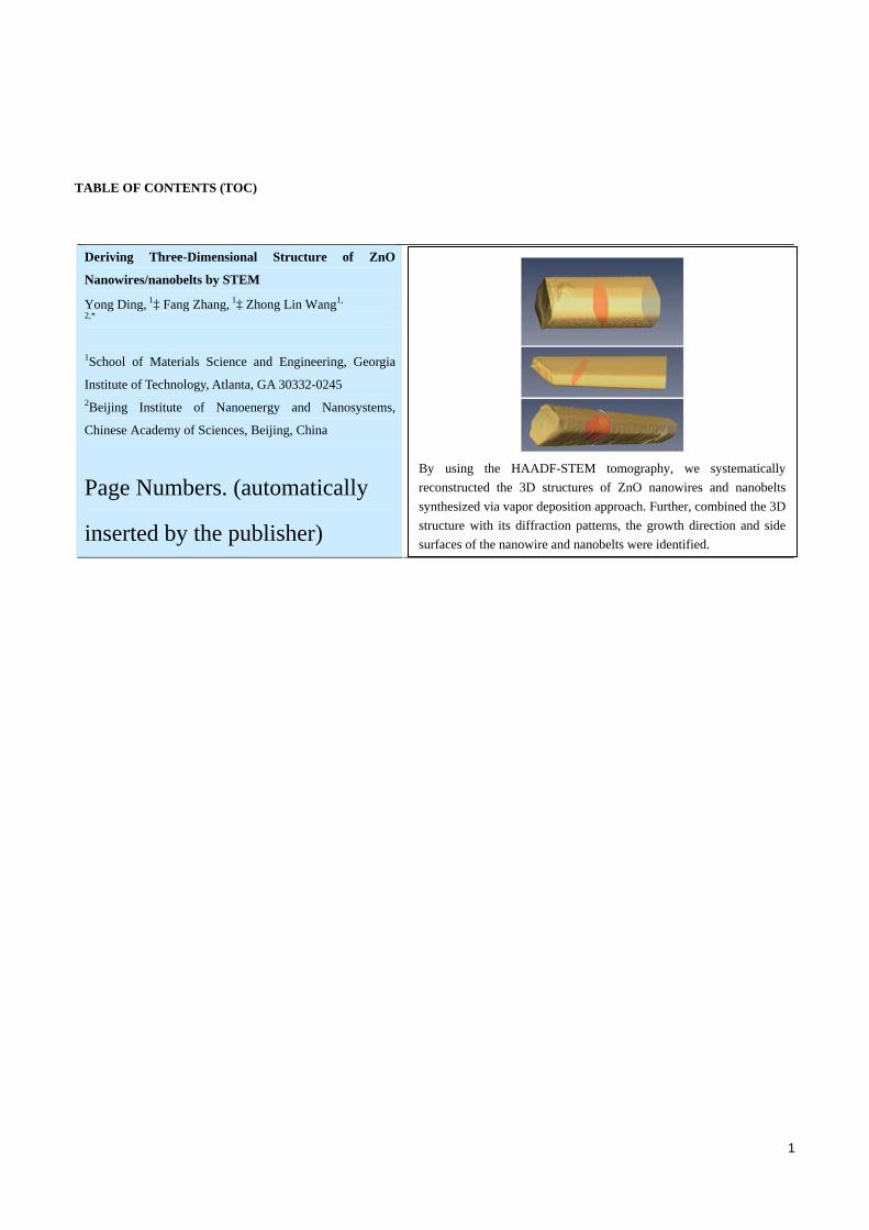
By using the HAADF-STEM tomography, we systematically
reconstructed the 3D structures of ZnO nanowires and nanobelts
synthesized via vapor deposition approach. Further, combined the 3D
structure with its diffraction patterns, the growth direction and side
surfaces of the nanowire and nanobelts were identified.
2
Deriving Three-Dimensional Structure of ZnO Nanowires/nanobelts by STEM Tomography
Yong Ding, 1‡ Fang Zhang, 1‡ Zhong Lin Wang1, 2() 1School of Materials Science and Engineering, Georgia Institute of Technology, Atlanta, GA 30332-0245, USA
2Beijing Institute of Nanoenergy and Nanosystems, Chinese Academy of Sciences, Beijing, China
‡ These authors contributed equally.
Received: day month year / Revised: day month year / Accepted: day month year (automatically inserted by the publisher) © Tsinghua University Press and Springer-Verlag Berlin Heidelberg 2011
ABSTRACT
Characterizing the three‐dimensional (3D) shape of a nanostructure by conventional imaging techniques in scanning electron microscopy and transmission electron microscopy can be limited or complexed by various factors, such as 2D projection, diffraction contrast and unsure orientation of the nanostructure with respect to the electron beam direction. In this paper, in conjunction with electron diffraction and imaging, the 3D morphologies of ZnO nanowires and nanobelts synthesized via vapor deposition approach were reconstructed by electron tomography in a scanning transmission electron microscope (STEM). The cross‐sections of these one‐dimensional nanostructures include triangle, hexagonal, and rectangle shapes. Combined the reconstructed shape with the crystalline information supplied by electron diffraction patterns recorded from the same nanowire/nanobelt, the growth direction and its exposed surfaces were uniquely identified. Totally three different growth directions were confirmed. These directions are <0001>, <2 0> and <2 3>, corresponding to <001>, <100> and <101> orientations in three‐index notation. The <0001> growth nanowires show triangle or hexagonal cross‐sections, with exposed {01 0} side surfaces. The dominant surfaces of the <2 > growth nanobelt are ± (0001) planes. Both hexagonal and rectangle cross‐sections were observed in the <2 3> growth ZnO nanostructures. Their surfaces include {01 0}, { 101} and { 112} planes. The nanobelts with a large aspect ratio ~ 10 normally grow along <2 0> direction, while nanobelts with small aspect ratio are along <2 3> growth direction. The approach and methodology demonstrated here can be extended to any nanostructures that can be crystalline, polycrystalline or even amorphous.
KEYWORDS ZnO, nanowire, nanobelt, TEM, STEM, electron tomography
1. Introduction
Quasi‐one‐dimensional (1D) ZnO
nanowires/nanobelts are the fundamental building
blocks for fabricating various devices such as field
Nano Res DOI (automatically inserted by the publisher) Research Article
———————————— Address correspondence to [email protected]
3
effect transistors [1, 2], nano‐LEDs [3, 4], gas‐sensor
[5, 6], force sensor [7, 8], nanogenerators [9, 10] and
piezotronic devices [11, 12]. Vapor phase deposition
[13, 14] and low‐temperature wet chemical or
hydrothermal methods [15, 16] are the two
well‐developed approaches to synthesize ZnO
nanostructures. Although the latter approach can
get well controlled uniform ZnO nanowire arrays
on different substrates, for the nanodevices built
using single ZnO nanostructure, the vapor
deposition approach is favorable for the following
reasons. Firstly, long nanowires/nanobelts are much
easy to manipulate during the device fabrication.
Vapor deposition method gives longer ZnO
nanowires/nanobelts, which can reach millimeter
scale, while the nanowires grown by wet chemical
approach are normally less than several
micrometers. Secondly, the crystallinity of the ZnO
nanowire will affect the electronic properties of the
nanodevices. Because of low working temperature
in the wet chemical method, normally around 100
°C [16], the crystallization of the nanowires is
relatively poorer compared with those synthesized
via the high‐temperature vapor deposition method
as long as the density of point defects is considered.
Thirdly, some applications are crystalline
orientation dependent, like the piezoelectric effect.
Most of the ZnO nanowires from wet chemical
approach are hexagonal shaped with unique
growth direction along <0001>, the c axis. While
vapor deposition method gives much more choices
if no catalyst used, growth directions other than
<0001> have been reported [17]. And not only
nanowires, but also nanobelts can be synthesized.
At the same time, different surfaces will be exposed
in these nanowires and nanobelts. In order to
optimize the performance of the nanodevices, we
need to choose the suitable ZnO nanostructures to
build the devices. Almost for all of the nanowire
based devices reported in the literature so far, only
the growth directions may be provided, and little
information is provided about the side facets, such
as the crystallography of the side surfaces and the
area ratio of each as well as the surface structures,
which are known from surface science point of view
of vitally importance for device performance. In
such a case, the surface structure is undefined,
which is likely to be a major weakness because the
performance of the nanowire devices is likely
dominated by the surfaces in many cases. In the
piezotronic devices, for instance, the
nanowire/nanobelt with large c plane as side
surfaces could be distinctly different from the
nanowire that is along the c‐axis owing to the
orientation of the crystal polarization [18, 19].
Alternatively, high‐index surfaces will benefit the
catalysis properties of the devices. Therefore, before
using the ZnO nanowires/nanobelts to build such
specified nanodevices, we need to fully characterize
their three‐dimension (3D) crystalline structures
including their growth directions and side surfaces.
Scanning electron microscopy (SEM) images
can give some rough information about the 3D
structure of nanomaterials with limited resolution,
but it is difficult to get the crystallographic
information at the same time. Traditionally,
transmission electron microscopy (TEM) is used to
collect the crystal structure information of
nanomaterials based on their selected‐area electron
diffraction (SAED) patterns and/or high‐resolution
TEM (HRTEM) images [20]. However, each TEM
image is only a two‐dimensional (2D) projection of
the real 3D object. It is difficult to explore the 3D
crystalline information of the nanomaterials solely
based on TEM images and diffraction patterns. The
routine methods for growth direction determination
include: Using the fast Fourier transformation (FFT)
of a high‐resolution transmission electron
microscopy (HRTEM) image recorded from the 1D
nanostructure; combining a low‐magnification
transmission electron microscopy (TEM) image
with its selected‐area electron diffraction (SAED)
pattern; or recording its shadow image [20].
However, the precondition for above methods
4
assumes that the incident electron beam is
perpendicular to the growth direction of 1D
nanostructures during we recorded the HRTEM
images and SAED patterns. In reality, such
assumption is not guaranteed anytime. Here we
determine the growth direction of ZnO 1D
nanostructures using two SAED patterns. Each
SAED pattern contains a special diffraction spot,
whose corresponded reciprocal vector
perpendicular to the growth direction. Then the
cross‐product of two of these vectors gives the
unique growth direction of the nanowire/nanobelt.
Electron tomography is a novel technique,
which can retrieve 3D structure information usually
missed in a conventional image [21]. A 3D structure
can be reconstructed by processing a series of
images taken by tilting the sample to different
orientations that the diffraction contrast is
minimized or largely eliminated in each image so
that the image contrast is proportional to the
projected mass‐thickness of the sample [22, 23].
Corresponding to different kinds of materials, we
need to choose the right imaging techniques to
fulfill the mass‐thickness contrast criteria. For
example, bright‐field TEM is suitable for
biomaterial and amorphous inorganic materials [24],
while the inorganic crystalline materials need to be
taken in scanning TEM (STEM) mode with the use
of a high‐angle annular dark‐field (HAADF)
detector, which collect a large angular range of
high‐angle scattered electrons so that the image
contrast is approximately proportional to the
mass‐thickness, and the diffraction contrast is
largely suppressed [25, 26]. For example, the STEM
tomography has been successfully applied to
reconstruct the 3D shape of some catalysis
nanoparticles [27‐35], TiO2 nanotubes [36], InAs
nanowires [37] and core‐shell GaP‐GaAs [38].
Here in this work, we first reconstructed the
3D morphologies of different ZnO nanowires and
nanobelts from a series of HAADF‐STEM images.
Then we switched to TEM mode and recorded the
SAED patterns from the same nanowire/nanobelt at
different tilting conditions. Combining the 3D
morphology and crystalline information, we have
uniquely identified the growth directions and all
their side surfaces of more than twenty ZnO
one‐dimension (1D) nanostructures. In statistics,
most of the nanowires grow along <0001> direction
and expose {01 0} side surfaces with cross‐section
in triangle or hexagonal shapes. The nanobelts
growing along <2 > direction have ± (0001)
dominant side surfaces. Other than the above two
growth directions, a new growth direction along
<2 3> was confirmed for the first time for both
nanowires and nanobelts. Their exposed large
surfaces belong to {01 0} plane, while the nanowire
shows some { 101} surfaces and the nanobelt show
some { 112} surfaces as well. The three growth
directions of <0001>, <2 0> and <2 3> are all
low‐indexed orientations in wurtzite structure.
They respectively correspond to the <001>, <100>
and <101> orientations in three‐index notation for
hexagonal structure.
2. Experimental details
The ZnO nanowires and nanobelts studied in this
work were synthesized using the vapor deposition
approach [13]. A FEI Tecnai F30 super‐twin
field‐emission gun TEM equipped with a single‐tilt
tomography holder from Fischione Instrument was
used to acquire the TEM images, SAED patterns
and the tilting series HAADF‐STEM images. During
the experiments, each nanowire/nanobelt was
aligned manually along the titling axis of the holder.
The tilt series were acquired over the tilt‐rang from
‐70° to 70° in STEM mode using Xplore 3D software
(FEI Company) by a step of 1° or 2° at different
angle ranges. The STEM HAADF images were
aligned using the IMOD software [39], and the 3D
reconstruction was performed using SIRT package
built in the Inspect3D software. The visualization of
the final 3D datasets was performed by using
5
isosurface or the voltex rendering in Amira V5.3.1
software. JEMS software was used to do the
electron diffraction simulation.
3. Results and discussion
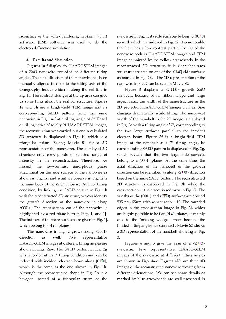
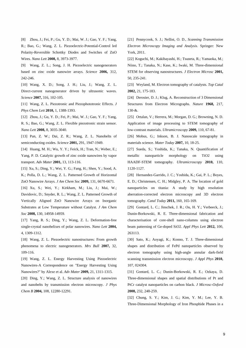
Figures 1a‐f display six HAADF‐STEM images
of a ZnO nanowire recorded at different tilting
angles. The axial direction of the nanowire has been
manually aligned to close to the tilting axis of the
tomography holder which is along the red line in
Fig. 1a. The contrast changes at the tip area can give
us some hints about the real 3D structure. Figures
1g and 1h are a bright‐field TEM image and its
corresponding SAED pattern from the same
nanowire in Fig. 1a‐f at a tilting angle of 8°. Based
on tilting series of totally 91 HAADF‐STEM images,
the reconstruction was carried out and a calculated
3D structure is displayed in Fig. 1i, which is a
triangular prism (Seeing Movie S1 for a 3D
representation of the nanowire). The displayed 3D
structure only corresponds to selected range of
intensity in the reconstruction. Therefore, we
missed the low‐contrast amorphous phase
attachment on the side surface of the nanowire as
shown in Fig. 1c, and what we observe in Fig. 1i is
the main body of the ZnO nanowire. At an 8° tilting
condition, by linking the SAED pattern in Fig. 1h
with the reconstructed 3D structure, we can identify
the growth direction of the nanowire is along
<0001>. The cross‐section cut of the nanowire is
highlighted by a red plane both in Figs. 1i and 1j.
The indexes of the three surfaces are given in Fig. 1j,
which belong to {01 0} planes.
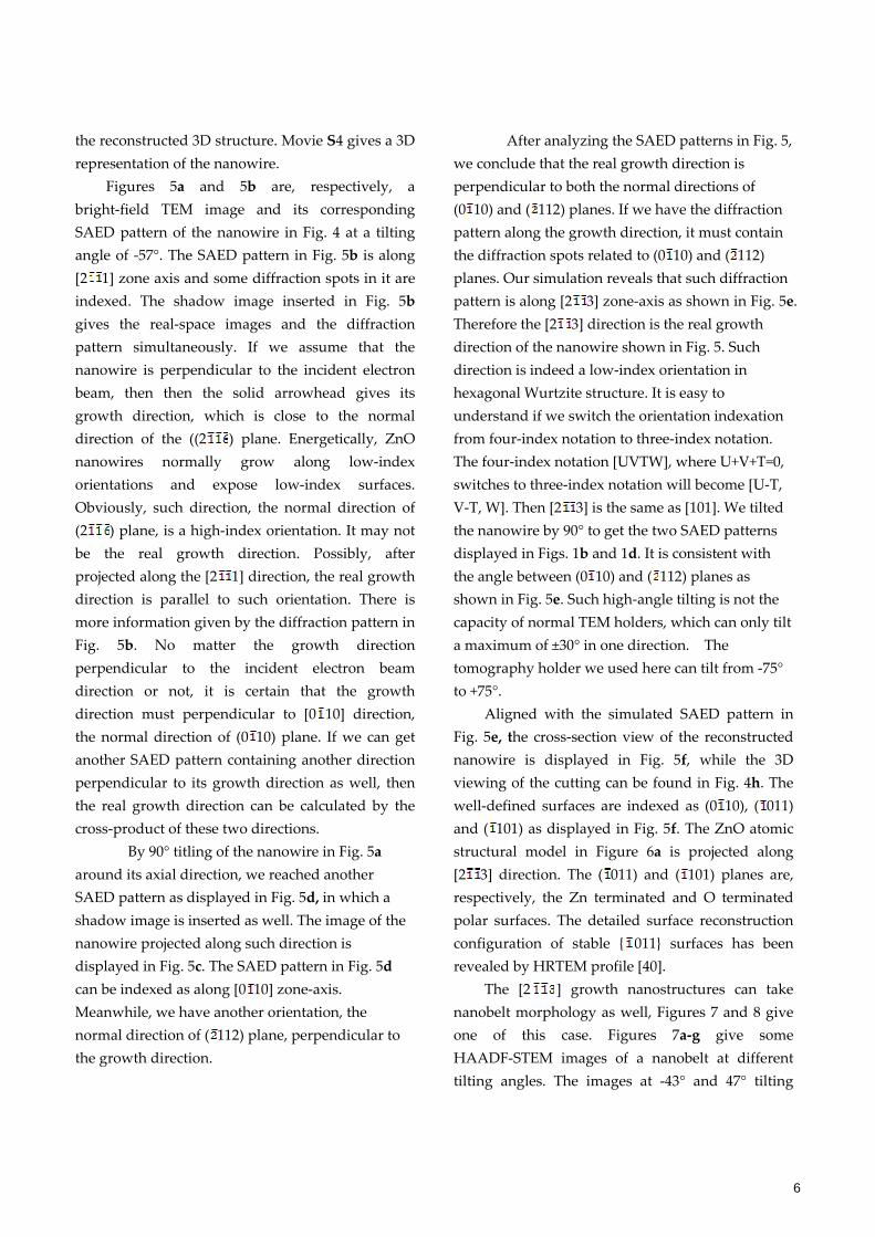
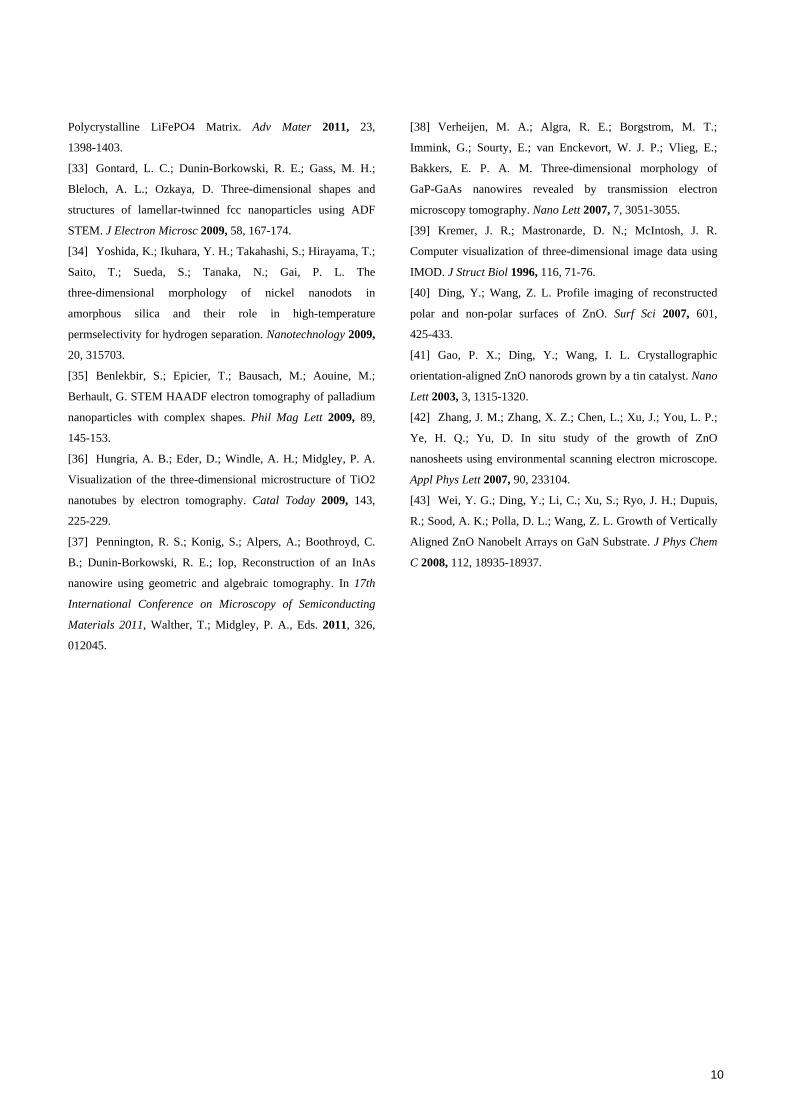
The nanowire in Fig. 2 grows along <0001>
direction as well. Five representative
HAADF‐STEM images at different tilting angles are
shown in Figs. 2a‐e. The SAED pattern in Fig. 2g
was recorded at an 1° tilting condition and can be
indexed with incident electron beam along [01 0],
which is the same as the one shown in Fig. 1h.
Although the reconstructed shape in Fig. 2h is a
hexagon instead of a triangular prism as the
nanowire in Fig. 1, its side surfaces belong to {01 0}
as well, which are indexed in Fig. 2i. It is noticeable
that here has a low‐contrast part at the tip of the
nanowire both in HAADF‐STEM images and TEM
image as pointed by the yellow arrowheads. In the
reconstructed 3D structure, it is clear that such
structure is seated on one of the {01 0} side surfaces
as marked in Fig. 2h. The 3D representation of the
nanowire in Fig. 2 can be seen in Movie S2.
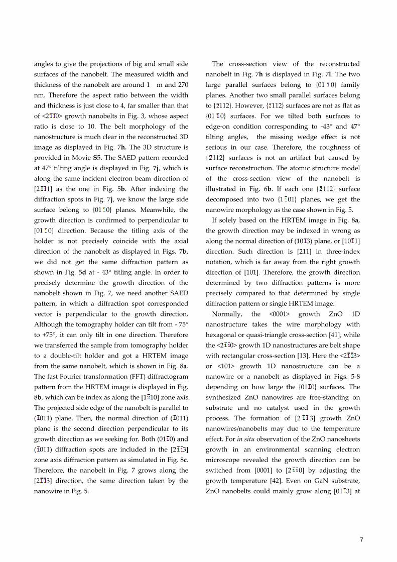
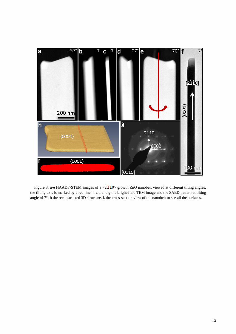
Figure 3 displays a <2 0> growth ZnO
nanobelt. Because of its ribbon shape and large
aspect ratio, the width of the nanostructure in the
2D projection HAADF‐STEM images in Figs. 3a‐e
changes dramatically while tilting. The narrowest
width of the nanobelt in the 2D image is displayed
in Fig. 3c with a tilting angle of 7°, corresponding to
the two large surfaces parallel to the incident
electron beam. Figure 3f is a bright‐field TEM
image of the nanobelt at a 7° tilting angle, its
corresponding SAED pattern is displayed in Fig. 3g,
which reveals that the two large side surfaces
belong to ± (0001) planes. At the same time, the
axial direction of the nanobelt or the growth
direction can be identified as along <2 0> direction
based on the same SAED pattern. The reconstructed
3D structure is displayed in Fig. 3h while the
cross‐section cut interface is redrawn in Fig. 3i. The
widths of the (0001) and (2 0) surfaces are around
535 nm, 55nm with aspect ratio ~ 10. The rounded
edges in the cross‐section image in Fig. 3i, which
are highly possible to be flat {01 0} planes, is mainly
due to the ʺmissing wedgeʺ effect, because the
limited tilting angles we can reach. Movie S3 shows
a 3D representation of the nanobelt showing in Fig.
3.
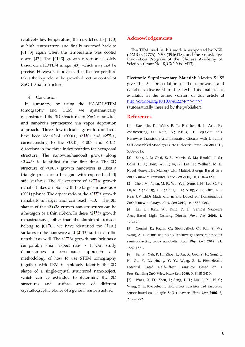
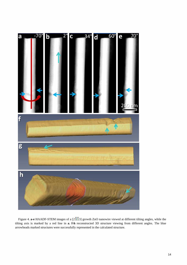
Figures 4 and 5 give the case of a <2 3>
nanowire. Five representative HAADF‐STEM
images of the nanowire at different tilting angles
are shown in Figs. 4a‐e. Figures 4f‐h are three 3D
images of the reconstructed nanowire viewing from
different orientations. We can see some details as
marked by blue arrowheads are well presented in
6
the reconstructed 3D structure. Movie S4 gives a 3D
representation of the nanowire.
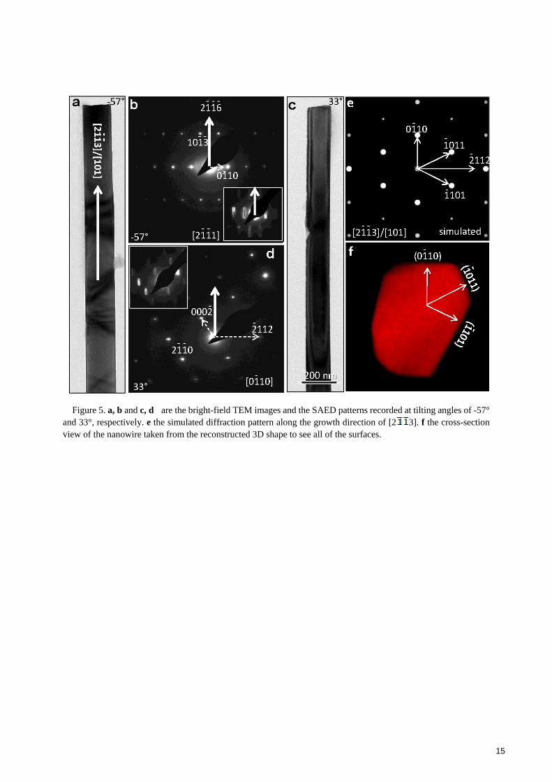
Figures 5a and 5b are, respectively, a
bright‐field TEM image and its corresponding
SAED pattern of the nanowire in Fig. 4 at a tilting
angle of ‐57°. The SAED pattern in Fig. 5b is along
[2 1] zone axis and some diffraction spots in it are
indexed. The shadow image inserted in Fig. 5b
gives the real‐space images and the diffraction
pattern simultaneously. If we assume that the
nanowire is perpendicular to the incident electron
beam, then then the solid arrowhead gives its
growth direction, which is close to the normal
direction of the ((2 ) plane. Energetically, ZnO
nanowires normally grow along low‐index
orientations and expose low‐index surfaces.
Obviously, such direction, the normal direction of
(2 ) plane, is a high‐index orientation. It may not
be the real growth direction. Possibly, after
projected along the [2 1] direction, the real growth
direction is parallel to such orientation. There is
more information given by the diffraction pattern in
Fig. 5b. No matter the growth direction
perpendicular to the incident electron beam
direction or not, it is certain that the growth
direction must perpendicular to [0 10] direction,
the normal direction of (0 10) plane. If we can get
another SAED pattern containing another direction
perpendicular to its growth direction as well, then
the real growth direction can be calculated by the
cross‐product of these two directions.
By 90° titling of the nanowire in Fig. 5a
around its axial direction, we reached another
SAED pattern as displayed in Fig. 5d, in which a
shadow image is inserted as well. The image of the
nanowire projected along such direction is
displayed in Fig. 5c. The SAED pattern in Fig. 5d
can be indexed as along [0 10] zone‐axis.
Meanwhile, we have another orientation, the
normal direction of ( 112) plane, perpendicular to
the growth direction.
After analyzing the SAED patterns in Fig. 5,
we conclude that the real growth direction is
perpendicular to both the normal directions of
(0 10) and ( 112) planes. If we have the diffraction
pattern along the growth direction, it must contain
the diffraction spots related to (0 10) and ( 112)
planes. Our simulation reveals that such diffraction
pattern is along [2 3] zone‐axis as shown in Fig. 5e.
Therefore the [2 3] direction is the real growth
direction of the nanowire shown in Fig. 5. Such
direction is indeed a low‐index orientation in
hexagonal Wurtzite structure. It is easy to
understand if we switch the orientation indexation
from four‐index notation to three‐index notation.
The four‐index notation [UVTW], where U+V+T=0,
switches to three‐index notation will become [U‐T,
V‐T, W]. Then [2 3] is the same as [101]. We tilted
the nanowire by 90° to get the two SAED patterns
displayed in Figs. 1b and 1d. It is consistent with
the angle between (0 10) and ( 112) planes as
shown in Fig. 5e. Such high‐angle tilting is not the
capacity of normal TEM holders, which can only tilt
a maximum of ±30° in one direction. The
tomography holder we used here can tilt from ‐75°
to +75°.
Aligned with the simulated SAED pattern in
Fig. 5e, the cross‐section view of the reconstructed
nanowire is displayed in Fig. 5f, while the 3D
viewing of the cutting can be found in Fig. 4h. The
well‐defined surfaces are indexed as (0 10), ( 011)
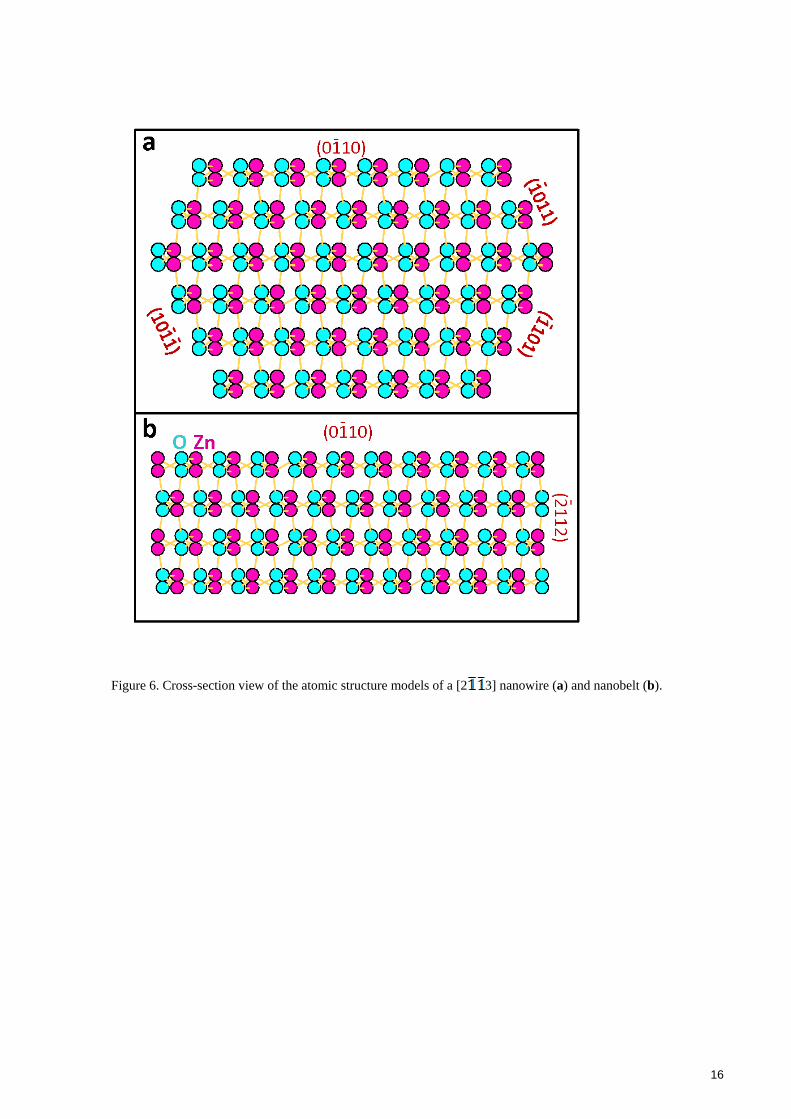
and ( 101) as displayed in Fig. 5f. The ZnO atomic
structural model in Figure 6a is projected along
[2 3] direction. The ( 011) and ( 101) planes are,
respectively, the Zn terminated and O terminated
polar surfaces. The detailed surface reconstruction
configuration of stable { 011} surfaces has been
revealed by HRTEM profile [40].
The [2 ] growth nanostructures can take
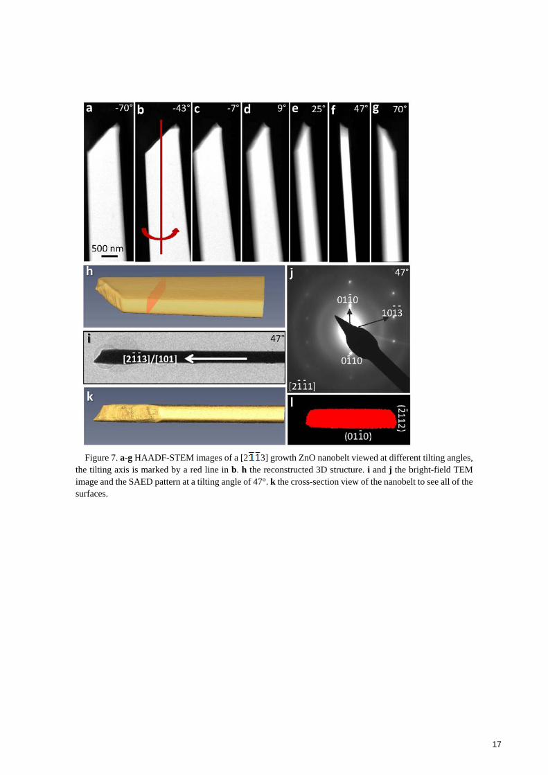
nanobelt morphology as well, Figures 7 and 8 give
one of this case. Figures 7a‐g give some
HAADF‐STEM images of a nanobelt at different
tilting angles. The images at ‐43° and 47° tilting
7
angles to give the projections of big and small side
surfaces of the nanobelt. The measured width and
thickness of the nanobelt are around 1 m and 270
nm. Therefore the aspect ratio between the width
and thickness is just close to 4, far smaller than that
of <2 0> growth nanobelts in Fig. 3, whose aspect
ratio is close to 10. The belt morphology of the
nanostructure is much clear in the reconstructed 3D
image as displayed in Fig. 7h. The 3D structure is
provided in Movie S5. The SAED pattern recorded
at 47° tilting angle is displayed in Fig. 7j, which is
along the same incident electron beam direction of
[2 1] as the one in Fig. 5b. After indexing the
diffraction spots in Fig. 7j, we know the large side
surface belong to {01 0} planes. Meanwhile, the
growth direction is confirmed to perpendicular to
[01 0] direction. Because the titling axis of the
holder is not precisely coincide with the axial
direction of the nanobelt as displayed in Figs. 7b,
we did not get the same diffraction pattern as
shown in Fig. 5d at ‐ 43° titling angle. In order to
precisely determine the growth direction of the
nanobelt shown in Fig. 7, we need another SAED
pattern, in which a diffraction spot corresponded
vector is perpendicular to the growth direction.
Although the tomography holder can tilt from ‐ 75°
to +75°, it can only tilt in one direction. Therefore
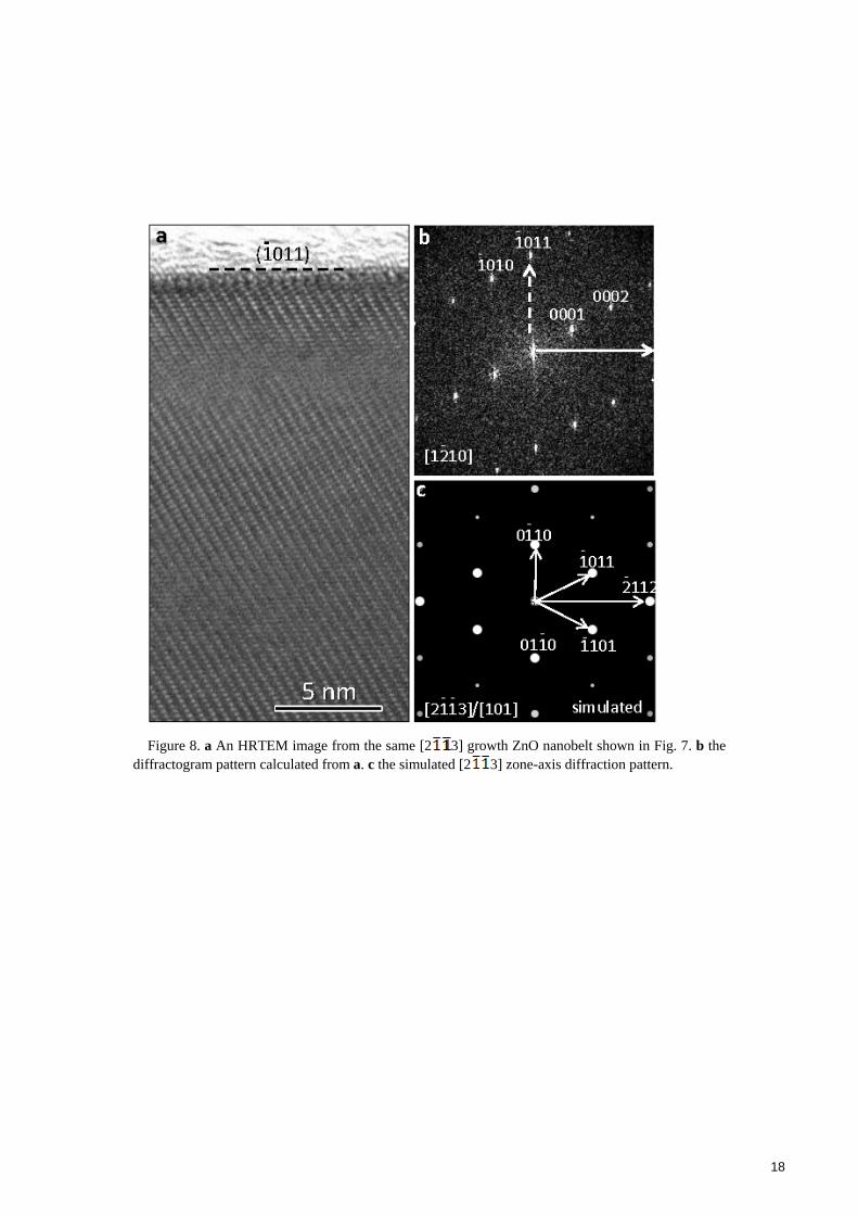
we transferred the sample from tomography holder
to a double‐tilt holder and got a HRTEM image
from the same nanobelt, which is shown in Fig. 8a.
The fast Fourier transformation (FFT) diffractogram
pattern from the HRTEM image is displayed in Fig.
8b, which can be index as along the [1 10] zone axis.
The projected side edge of the nanobelt is parallel to
( 011) plane. Then, the normal direction of ( 011)
plane is the second direction perpendicular to its
growth direction as we seeking for. Both (01 0) and
( 011) diffraction spots are included in the [2 3]
zone axis diffraction pattern as simulated in Fig. 8c.
Therefore, the nanobelt in Fig. 7 grows along the
[2 3] direction, the same direction taken by the
nanowire in Fig. 5.
The cross‐section view of the reconstructed
nanobelt in Fig. 7h is displayed in Fig. 7l. The two
large parallel surfaces belong to {01 0} family
planes. Another two small parallel surfaces belong
to { 112}. However, { 112} surfaces are not as flat as
{01 0} surfaces. For we tilted both surfaces to
edge‐on condition corresponding to ‐43° and 47°
tilting angles, the missing wedge effect is not
serious in our case. Therefore, the roughness of
{ 112} surfaces is not an artifact but caused by
surface reconstruction. The atomic structure model
of the cross‐section view of the nanobelt is
illustrated in Fig. 6b. If each one { 112} surface
decomposed into two {1 01} planes, we get the
nanowire morphology as the case shown in Fig. 5.
If solely based on the HRTEM image in Fig. 8a,
the growth direction may be indexed in wrong as
along the normal direction of (10 3) plane, or [10 1]
direction. Such direction is [211] in three‐index
notation, which is far away from the right growth
direction of [101]. Therefore, the growth direction
determined by two diffraction patterns is more
precisely compared to that determined by single
diffraction pattern or single HRTEM image.
Normally, the <0001> growth ZnO 1D
nanostructure takes the wire morphology with
hexagonal or quasi‐triangle cross‐section [41], while
the <2 0> growth 1D nanostructures are belt shape
with rectangular cross‐section [13]. Here the <2 3>
or <101> growth 1D nanostructure can be a
nanowire or a nanobelt as displayed in Figs. 5‐8
depending on how large the {01 0} surfaces. The
synthesized ZnO nanowires are free‐standing on
substrate and no catalyst used in the growth
process. The formation of [2 3] growth ZnO
nanowires/nanobelts may due to the temperature
effect. For in situ observation of the ZnO nanosheets
growth in an environmental scanning electron
microscope revealed the growth direction can be
switched from [0001] to [2 0] by adjusting the
growth temperature [42]. Even on GaN substrate,
ZnO nanobelts could mainly grow along [01 3] at
8
relatively low temperature, then switched to [01 0]
at high temperature, and finally switched back to
[01 3] again when the temperature was cooled
down [43]. The [01 3] growth direction is solely
based on a HRTEM image [43], which may not be
precise. However, it reveals that the temperature
takes the key role in the growth direction control of
ZnO 1D nanostructure.
4. Conclusion
In summary, by using the HAADF‐STEM
tomography and TEM, we systematically
reconstructed the 3D structures of ZnO nanowires
and nanobelts synthesized via vapor deposition
approach. Three low‐indexed growth directions
have been identified: <0001>, <2 0> and <2 >,
corresponding to the <001>, <100> and <101>
directions in the three‐index notation for hexagonal
structure. The nanowire/nanobelt grows along
<2 3> is identified for the first time. The 3D
structure of <0001> growth nanowires is likes a
triangle prism or a hexagon with exposed {01 0}
side surfaces. The 3D structure of <2 0> growth
nanobelt likes a ribbon with the large surfaces as ±
(0001) planes. The aspect ratio of the <2 0> growth
nanobelts is larger and can reach ~10. The 3D
shapes of the <2 3> growth nanostructures can be
a hexagon or a thin ribbon. In these <2 3> growth
nanostructures, other than the dominant surfaces
belong to {01 0}, we have identified the { 101}
surfaces in the nanowire and { 112} surfaces in the
nanobelt as well. The <2 3> growth nanobelt has a
comparably small aspect ratio ~ 4. Our study
demonstrates a systematic approach and
methodology of how to use STEM tomography
together with TEM to uniquely identify the 3D
shape of a single‐crystal structured nano‐object,
which can be extended to determine the 3D
structures and surface areas of different
crystallographic planes of a general nanostructure.
Acknowledgements The TEM used in this work is supported by NSF
(DMR 0922776), NSF (0946418), and the Knowledge Innovation Program of the Chinese Academy of Sciences Grant No. KJCX2‐YW‐M13).
Electronic Supplementary Material: Movies S1‐S5
give the 3D presentation of the nanowires and
nanobelts discussed in the text. This material is
available in the online version of this article at
http://dx.doi.org/10.1007/s12274‐***‐****‐*
(automatically inserted by the publisher). References [1] Kaelblein, D.; Weitz, R. T.; Bottcher, H. J.; Ante, F.;
Zschieschang, U.; Kern, K.; Klauk, H. Top-Gate ZnO
Nanowire Transistors and Integrated Circuits with Ultrathin
Self-Assembled Monolayer Gate Dielectric. Nano Lett 2011, 11,
5309-5315.
[2] Sohn, J. I.; Choi, S. S.; Morris, S. M.; Bendall, J. S.;
Coles, H. J.; Hong, W. K.; Jo, G.; Lee, T.; Welland, M. E.
Novel Nonvolatile Memory with Multibit Storage Based on a
ZnO Nanowire Transistor. Nano Lett 2010, 10, 4316-4320.
[3] Chen, M. T.; Lu, M. P.; Wu, Y. J.; Song, J. H.; Lee, C. Y.;
Lu, M. Y.; Chang, Y. C.; Chou, L. J.; Wang, Z. L.; Chen, L. J.
Near UV LEDs Made with in Situ Doped p-n Homojunction
ZnO Nanowire Arrays. Nano Lett 2010, 10, 4387-4393.
[4] Lai, E.; Kim, W.; Yang, P. D. Vertical Nanowire
Array-Based Light Emitting Diodes. Nano Res 2008, 1,
123-128.
[5] Comini, E.; Faglia, G.; Sberveglieri, G.; Pan, Z. W.;
Wang, Z. L. Stable and highly sensitive gas sensors based on
semiconducting oxide nanobelts. Appl Phys Lett 2002, 81,
1869-1871.
[6] Fei, P.; Yeh, P. H.; Zhou, J.; Xu, S.; Gao, Y. F.; Song, J.
H.; Gu, Y. D.; Huang, Y. Y.; Wang, Z. L. Piezoelectric
Potential Gated Field-Effect Transistor Based on a
Free-Standing ZnO Wire. Nano Lett 2009, 9, 3435-3439.
[7] Wang, X. D.; Zhou, J.; Song, J. H.; Liu, J.; Xu, N. S.;
Wang, Z. L. Piezoelectric field effect transistor and nanoforce
sensor based on a single ZnO nanowire. Nano Lett 2006, 6,
2768-2772.
9
[8] Zhou, J.; Fei, P.; Gu, Y. D.; Mai, W. J.; Gao, Y. F.; Yang,
R.; Bao, G.; Wang, Z. L. Piezoelectric-Potential-Control led
Polarity-Reversible Schottky Diodes and Switches of ZnO
Wires. Nano Lett 2008, 8, 3973-3977.
[9] Wang, Z. L.; Song, J. H. Piezoelectric nanogenerators
based on zinc oxide nanowire arrays. Science 2006, 312,
242-246.
[10] Wang, X. D.; Song, J. H.; Liu, J.; Wang, Z. L.
Direct-current nanogenerator driven by ultrasonic waves.
Science 2007, 316, 102-105.
[11] Wang, Z. L. Piezotronic and Piezophototronic Effects. J
Phys Chem Lett 2010, 1, 1388-1393.
[12] Zhou, J.; Gu, Y. D.; Fei, P.; Mai, W. J.; Gao, Y. F.; Yang,
R. S.; Bao, G.; Wang, Z. L. Flexible piezotronic strain sensor.
Nano Lett 2008, 8, 3035-3040.
[13] Pan, Z. W.; Dai, Z. R.; Wang, Z. L. Nanobelts of
semiconducting oxides. Science 2001, 291, 1947-1949.
[14] Huang, M. H.; Wu, Y. Y.; Feick, H.; Tran, N.; Weber, E.;
Yang, P. D. Catalytic growth of zinc oxide nanowires by vapor
transport. Adv Mater 2001, 13, 113-116.
[15] Xu, S.; Ding, Y.; Wei, Y. G.; Fang, H.; Shen, Y.; Sood, A.
K.; Polla, D. L.; Wang, Z. L. Patterned Growth of Horizontal
ZnO Nanowire Arrays. J Am Chem Soc 2009, 131, 6670-6671.
[16] Xu, S.; Wei, Y.; Kirkham, M.; Liu, J.; Mai, W.;
Davidovic, D.; Snyder, R. L.; Wang, Z. L. Patterned Growth of
Vertically Aligned ZnO Nanowire Arrays on Inorganic
Substrates at Low Temperature without Catalyst. J Am Chem
Soc 2008, 130, 14958-14959.
[17] Yang, R. S.; Ding, Y.; Wang, Z. L. Deformation-free
single-crystal nanohelixes of polar nanowires. Nano Lett 2004,
4, 1309-1312.
[18] Wang, Z. L. Piezoelectric nanostructures: From growth
phenomena to electric nanogenerators. Mrs Bull 2007, 32,
109-116.
[19] Wang, Z. L. Energy Harvesting Using Piezoelectric
Nanowires-A Correspondence on "Energy Harvesting Using
Nanowires?" by Alexe et al. Adv Mater 2009, 21, 1311-1315.
[20] Ding, Y.; Wang, Z. L. Structure analysis of nanowires
and nanobelts by transmission electron microscopy. J Phys
Chem B 2004, 108, 12280-12291.
[21] Pennycook, S. J.; Nellist, O. D., Scanning Transmission
Electron Microscopy Imaging and Analysis. Springer: New
York, 2011.
[22] Koguchi, M.; Kakibayashi, H.; Tsuneta, R.; Yamaoka, M.;
Niino, T.; Tanaka, N.; Kase, K.; Iwaki, M. Three-dimensional
STEM for observing nanostructures. J Electron Microsc 2001,
50, 235-241.
[23] Weyland, M. Electron tomography of catalysts. Top Catal
2002, 21, 175-183.
[24] Derosier, D. J.; Klug, A. Reconstruction of 3 Dimensional
Structures from Electron Micrographs. Nature 1968, 217,
130-&.
[25] Ortalan, V.; Herrera, M.; Morgan, D. G.; Browning, N. D.
Application of image processing to STEM tomography of
low-contrast materials. Ultramicroscopy 2009, 110, 67-81.
[26] Mobus, G.; Inkson, B. J. Nanoscale tomography in
materials science. Mater Today 2007, 10, 18-25.
[27] Sueda, S.; Yoshida, K.; Tanaka, N. Quantification of
metallic nanoparticle morphology on TiO2 using
HAADF-STEM tomography. Ultramicroscopy 2010, 110,
1120-1127.
[28] Hernandez-Garrido, J. C.; Yoshida, K.; Gai, P. L.; Boyes,
E. D.; Christensen, C. H.; Midgley, P. A. The location of gold
nanoparticles on titania: A study by high resolution
aberration-corrected electron microscopy and 3D electron
tomography. Catal Today 2011, 160, 165-169.
[29] Gontard, L. C.; Jinschek, J. R.; Ou, H. Y.; Verbeeck, J.;
Dunin-Borkowski, R. E. Three-dimensional fabrication and
characterisation of core-shell nano-columns using electron
beam patterning of Ge-doped SiO2. Appl Phys Lett 2012, 100,
263113.
[30] Sato, K.; Aoyagi, K.; Konno, T. J. Three-dimensional
shapes and distribution of FePd nanoparticles observed by
electron tomography using high-angle annular dark-field
scanning transmission electron microscopy. J Appl Phys 2010,
107, 024304.
[31] Gontard, L. C.; Dunin-Borkowski, R. E.; Ozkaya, D.
Three-dimensional shapes and spatial distributions of Pt and
PtCr catalyst nanoparticles on carbon black. J Microsc-Oxford
2008, 232, 248-259.
[32] Chung, S. Y.; Kim, J. G.; Kim, Y. M.; Lee, Y. B.
Three-Dimensional Morphology of Iron Phosphide Phases in a
10
Polycrystalline LiFePO4 Matrix. Adv Mater 2011, 23,
1398-1403.
[33] Gontard, L. C.; Dunin-Borkowski, R. E.; Gass, M. H.;
Bleloch, A. L.; Ozkaya, D. Three-dimensional shapes and
structures of lamellar-twinned fcc nanoparticles using ADF
STEM. J Electron Microsc 2009, 58, 167-174.
[34] Yoshida, K.; Ikuhara, Y. H.; Takahashi, S.; Hirayama, T.;
Saito, T.; Sueda, S.; Tanaka, N.; Gai, P. L. The
three-dimensional morphology of nickel nanodots in
amorphous silica and their role in high-temperature
permselectivity for hydrogen separation. Nanotechnology 2009,
20, 315703.
[35] Benlekbir, S.; Epicier, T.; Bausach, M.; Aouine, M.;
Berhault, G. STEM HAADF electron tomography of palladium
nanoparticles with complex shapes. Phil Mag Lett 2009, 89,
145-153.
[36] Hungria, A. B.; Eder, D.; Windle, A. H.; Midgley, P. A.
Visualization of the three-dimensional microstructure of TiO2
nanotubes by electron tomography. Catal Today 2009, 143,
225-229.
[37] Pennington, R. S.; Konig, S.; Alpers, A.; Boothroyd, C.
B.; Dunin-Borkowski, R. E.; Iop, Reconstruction of an InAs
nanowire using geometric and algebraic tomography. In 17th
International Conference on Microscopy of Semiconducting
Materials 2011, Walther, T.; Midgley, P. A., Eds. 2011, 326,
012045.
[38] Verheijen, M. A.; Algra, R. E.; Borgstrom, M. T.;
Immink, G.; Sourty, E.; van Enckevort, W. J. P.; Vlieg, E.;
Bakkers, E. P. A. M. Three-dimensional morphology of
GaP-GaAs nanowires revealed by transmission electron
microscopy tomography. Nano Lett 2007, 7, 3051-3055.
[39] Kremer, J. R.; Mastronarde, D. N.; McIntosh, J. R.
Computer visualization of three-dimensional image data using
IMOD. J Struct Biol 1996, 116, 71-76.
[40] Ding, Y.; Wang, Z. L. Profile imaging of reconstructed
polar and non-polar surfaces of ZnO. Surf Sci 2007, 601,
425-433.
[41] Gao, P. X.; Ding, Y.; Wang, I. L. Crystallographic
orientation-aligned ZnO nanorods grown by a tin catalyst. Nano
Lett 2003, 3, 1315-1320.
[42] Zhang, J. M.; Zhang, X. Z.; Chen, L.; Xu, J.; You, L. P.;
Ye, H. Q.; Yu, D. In situ study of the growth of ZnO
nanosheets using environmental scanning electron microscope.
Appl Phys Lett 2007, 90, 233104.
[43] Wei, Y. G.; Ding, Y.; Li, C.; Xu, S.; Ryo, J. H.; Dupuis,
R.; Sood, A. K.; Polla, D. L.; Wang, Z. L. Growth of Vertically
Aligned ZnO Nanobelt Arrays on GaN Substrate. J Phys Chem
C 2008, 112, 18935-18937.
11
Figure 1. a-f HAADF-STEM images of a <0001> growth ZnO nanowire viewed at different tilting angles, while the
tilting axis is marked by a red line in a. g and h the bright-field TEM image and the SAED pattern at a tilting angle of 8°.
i the reconstructed 3D structure. j the cross-section view of the nanowire to see all of the surfaces
FIGURES
12
Figure 2. a-e HAADF STEM images of a <0001> growth ZnO nanowire viewed at different tilting angles, the
tilting axis is marked by a red line in b. f and g the bright-field TEM image and the SAED pattern at a tilting
angle of 1°. h the reconstructed 3D structure. i. the cross-section view of the nanowire to see all the surfaces.
13
Figure 3. a-e HAADF-STEM images of a <2 0> growth ZnO nanobelt viewed at different tilting angles, the tilting axis is marked by a red line in e. f and g the bright-field TEM image and the SAED pattern at tilting angle of 7°. h the reconstructed 3D structure. i. the cross-section view of the nanobelt to see all the surfaces.
14
Figure 4. a-e HAADF-STEM images of a [2 3] growth ZnO nanowire viewed at different tilting angles, while the tilting axis is marked by a red line in a. f-h reconstructed 3D structure viewing from different angles. The blue arrowheads marked structures were successfully represented in the calculated structure.
15
Figure 5. a, b and c, d are the bright-field TEM images and the SAED patterns recorded at tilting angles of -57° and 33°, respectively. e the simulated diffraction pattern along the growth direction of [2 3]. f the cross-section view of the nanowire taken from the reconstructed 3D shape to see all of the surfaces.
16
Figure 6. Cross-section view of the atomic structure models of a [2 3] nanowire (a) and nanobelt (b).
17
Figure 7. a-g HAADF-STEM images of a [2 3] growth ZnO nanobelt viewed at different tilting angles,
the tilting axis is marked by a red line in b. h the reconstructed 3D structure. i and j the bright-field TEM image and the SAED pattern at a tilting angle of 47°. k the cross-section view of the nanobelt to see all of the surfaces.
18
Figure 8. a An HRTEM image from the same [2 3] growth ZnO nanobelt shown in Fig. 7. b the
diffractogram pattern calculated from a. c the simulated [2 3] zone-axis diffraction pattern.