Embed Size (px)
Citation preview
697Sensors and Materials, Vol. 31, No. 3 (2019) 697–711MYU Tokyo
S & M 1807
*Corresponding author: e-mail: [email protected]://doi.org/10.18494/SAM.2019.2063
ISSN 0914-4935 © MYU K.K.https://myukk.org/
Design and Development of Fan-shaped Silicon Resonatorsfor Young’s Modulus Measurement
Takahiro Namazu,1* Junki Kuroishi,2 Hiroya Yamagiwa,2 Daisuke Goto,2
Tatsuya Takeuchi,3 Kohei Murakami,3 Yasushi Kawashimo,3 and Tetsuo Takano4
1Department of Mechanical Engineering, Aichi Institute of Technology,1247 Yachigusa, Yakusa, Toyota, Aichi 470-0392, Japan
2Department of Mechanical Engineering, University of Hyogo, 2167 Shosha, Himeji, Hyogo 671-2201, Japan3Sinko Seiki Co., Ltd., 1-35-3 Takatsukadai, Nishi, Kobe, Hyogo 651-2271, Japan
4The New Industry Research Organization, 1-5-2 Minatojima Minamimachi, Chuo, Kobe, Hyogo 650-0047, Japan
(Received July 22, 2018; accepted November 1, 2018)
Keywords: single-crystal silicon, MEMS resonator, mechanical property measurement, Young’s modulus, resonant frequency
In this paper, the structural design and experiment of MEMS resonators for accurately measuring Young’s modulus is described. To establish an accurate measurement technique for the Young’s modulus of nanometer-thick thin films, first, we design MEMS resonators that can accurately derive the Young’s modulus of a structural material. The designed resonators are fan-shaped and can vibrate sympathetically in-plane. In total, the shape and dimensions of eleven mechanical parts in a resonator are considered using finite element (FE) analyses, and it is shown that the thickness-to-width ratio and the length of the rotation support beam affect the derivation of Young’s modulus. After device design, we fabricate the resonators made of single-crystal Si (SCS) using three different etching techniques: Bosch process deep reactive ion etching (DRIE), non-Bosch DRIE, and focused ion beam (FIB) etching. When the resonators fabricated by non-Bosch DRIE and FIB etching are used, experimentally obtained Young’s moduli are comparable to FE-analyses-derived Young’s moduli. The resonators with a long rotation support beam and a large thickness-to-width ratio of the beam can provide Young’s moduli that are close to the ideal value. However, Young’s moduli obtained from the resonators fabricated by the Bosch process DRIE differ largely from FE-analyses-derived Young’s moduli. The sidewall effect is discussed in the light of the modal analyses by the FE method.
1. Introduction
Young’s modulus of materials is, needless to say, one of the significant material characteristics required to design mechanical elements.(1) For a reliable design, specimens with a practically used size should be prepared first via a practically applied process history; then, experimentally measuring Young’s modulus is important. The obtained information should be reflected in the structural design. For micron-sized devices, such as semiconductor devices and
698 Sensors and Materials, Vol. 31, No. 3 (2019)
MEMS, the design approach is the same as that for large machines in that a large safety factor is required. Representative reliable testing techniques for experimentally measuring Young’s modulus of micron-sized structures are the uniaxial tensile test,(2–8) bending test,(9–11) and resonance test.(12–19) The uniaxial tensile test is popular for micron-sized specimens as well as bulk specimens. The biggest advantage is that it can be used to directly obtain the stress–strain relationship, which includes many significant mechanical properties, such as Young’s modulus, yield strength, and fracture strength. If the lateral strain in addition to the longitudinal strain can be experimentally measured, Poisson’s ratio can be obtained. For example, Sharpe Jr. et al.,(20) Cho et al.,(21) and Namazu et al.(22,23) have developed direct measurement techniques for transversal strain or out-of-plane strain of micron-sized specimens during uniaxial tensile loading and have successfully measured Poisson’s ratio in addition to Young’s modulus. Their techniques are excellent, but very tricky and complicated; therefore, these versatilities are not so high. The bending test is also as popular as the tensile test because of easy sample preparation and easy bending force application. For small specimens, however, setting the specimens onto a sample holder and finely measuring the deformation are technically difficult. The resonance test is a technique for directly measuring Young’s modulus of micron-sized specimens. This test is superior to other mechanical tests because of its simple test setup; that is, the actuator, load cell, and displacement meter that are necessary for typical mechanical tests are not required. If the specimen size and dimensions are known prior to the test, Young’s modulus can be derived merely by measuring the resonant frequency. The resonance test can be categorized into two methods: out-of-plane resonance test(24–26) and in-plane resonance test.(27,28) The out-of-plane resonance test can work well as a Young’s modulus measurement method for the resonator by itself, but it is difficult to use the method for nanometer-thick films deposited on the resonator because of a difference in strain distribution between the film and the substrate. By contrast, the in-plane resonance test has the potential to measure Young’s modulus of both the film and the substrate because the strain distribution in the film is the same as that in the substrate. By using the in-plane resonance method, we focus on developing a quantitative and simple experimental technique for measuring the Young’s modulus of micron-sized specimens. The final goal of this project is to establish a complete experimental technique for nanometer-thick films without the need for an operator’s special skills. Before the experiments for nanometer-thick films, Young’s modulus of a resonator material must be accurately measured. In this paper, therefore, we describe the design and development of in-plane-motion MEMS resonators made of single-crystal Si (SCS) for the accurate measurement of Young’s modulus. For the structural design, static bending and modal analyses by the finite element (FE) method are conducted. The shape and dimensions of the resonators are determined for accurately measuring Young’s modulus. For the fabrication, three etching techniques, namely, “Bosch process deep reactive ion etching (DRIE)”, non-Bosch DRIE, and focused ion beam (FIB) etching, are employed. The effects of device dimensions and sidewall shape on Young’s modulus are discussed.

Sensors and Materials, Vol. 31, No. 3 (2019) 699
2. Concept
Figure 1 shows a schematic of the designed MEMS resonator. Muhlstein et al. developed this type of device for investigating fatigue in SCS and polycrystal silicon.(16–19,29,30) We have adapted their device to enable Young’s modulus measurement. The resonator is composed of a fan-shaped vibration body, a set of comb-drive electrostatic actuators for resonance motion application, a set of capacitive sensors for vibration amplitude measurement, a gauge for measurement using a CCD image analysis system, and a rectangular solid beam for rotation support. The resonator is connected to a substrate at only one point via a support beam. On the basis of the linear elastic theory for isotropic materials, the resonant frequency f for this type of resonator can be expressed as(31,32)
12
kfJπ
= , (1)
where k and J are the spring constant of the rotation support beam and the moment of inertia of the resonator, respectively. The designed MEMS resonator can show many frequency variations. Among them, out-of-plane bending, in-plane bending, and twisting are dominant. For accurately and simply measuring Young’s modulus of a nanometer-thick film using this resonator, in-plane vibration
Fig. 1. Schematic of fan-shaped in-plane-motion MEMS resonator. The dimensions of all the mechanical parts were considered in the derivation of Young’s modulus.

700 Sensors and Materials, Vol. 31, No. 3 (2019)
is the best choice because the strain distribution in the film layer deposited on the resonator is identical to that in the resonator.(33) Therefore, we have chosen the in-plane resonant frequency of the first mode to determine Young’s moduli of both the film and the substrate. In in-plane bending vibrations, k of the rotation support beam is expressed as(34)
3
,12
EI Etwkl l
= = (2)
where E is Young’s modulus of the beam, I is the geometrical moment of inertia, and l, t, and w are the length, thickness, and width of the beam, respectively. J of the resonator rotating in-plane around the center of the beam can be expressed as the sum of the moments of inertia for the fan-shaped portion, Jf, the comb structure portion, Jc, and the gauge portion, Jg, which are, respectively, given by(15)
2 41 ,4fJ r dm t Rρ ϕ= =∫ (3)
( ) ( ){ }1 1
4 42 3
0 0
12 ,2
m ma bm cc a bn
n nJ r dm t r dr t a bn c a bnρ ψ ρ ψ
− −+ +
+= =
= = = + + − +∑ ∑∫ ∫ (4)
( )2 22 2
2 21 ,12 2 12 2g
h d h hJ d h dht R dht dht Rρ ρ ρ + = + + + = + +
(5)
where ρ is the density of the resonator. Dimensional parameters in these equations are defined in Fig. 1. From Eqs. (3)–(5), J is given by
( ) ( ){ } ( )2 21
4 4 24
0
1 2 2 .4 3
m
n
d hJ t R a bn c a bn dh R hρ ϕ ψ−
=
+ = + + + − + + + +
∑ (6)
By substituting Eqs. (2) and (6) into Eq. (1), Young’s modulus E of the resonator can be derived as
( )2 332 ,l XE f
wρπ= (7)
where X represents the terms inside the large square brackets in Eq. (6). All the parameters included in Eq. (7) are the material constants or the dimensions except for the resonant frequency f. Thus, if f is experimentally measured, E can be directly obtained.
Sensors and Materials, Vol. 31, No. 3 (2019) 701
3. Device Design
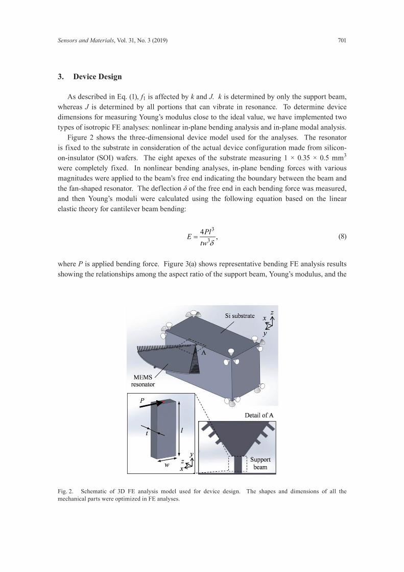
As described in Eq. (1), f1 is affected by k and J. k is determined by only the support beam, whereas J is determined by all portions that can vibrate in resonance. To determine device dimensions for measuring Young’s modulus close to the ideal value, we have implemented two types of isotropic FE analyses: nonlinear in-plane bending analysis and in-plane modal analysis. Figure 2 shows the three-dimensional device model used for the analyses. The resonator is fixed to the substrate in consideration of the actual device configuration made from silicon-on-insulator (SOI) wafers. The eight apexes of the substrate measuring 1 × 0.35 × 0.5 mm3 were completely fixed. In nonlinear bending analyses, in-plane bending forces with various magnitudes were applied to the beam’s free end indicating the boundary between the beam and the fan-shaped resonator. The deflection δ of the free end in each bending force was measured, and then Young’s moduli were calculated using the following equation based on the linear elastic theory for cantilever beam bending:
3
34 ,PlEtw δ
= (8)
where P is applied bending force. Figure 3(a) shows representative bending FE analysis results showing the relationships among the aspect ratio of the support beam, Young’s modulus, and the
Fig. 2. Schematic of 3D FE analysis model used for device design. The shapes and dimensions of all the mechanical parts were optimized in FE analyses.

702 Sensors and Materials, Vol. 31, No. 3 (2019)
difference between FE-analyses-derived Young’s modulus and the ideal value. In this paper, the thickness-to-width ratio of the beam was defined as the aspect ratio. The white, gray, and black plots are the results for the resonators with support beam lengths of 50, 100, and 200 µm, respectively. All the moduli were calculated using the deflections when the rotation angle of resonators was 4° because the angle range was designed to be within ±5°. When the aspect ratio was 0.2, Young’s moduli for 50-, 100-, and 200-µm-long beam resonators were calculated to be 90.2, 142.2, and 161.2 GPa, respectively, which were 46.6, 15.8, and 4.2% smaller than the ideal value, 168.9 GPa.(35) With an increase in the aspect ratio, the moduli were markedly increased. Young’s moduli of the resonators with the beam lengths of 50, 100, and 200 µm were almost the same as the ideal value when the ratios were 2.0, 1.0, and 0.5, respectively. The reason why the modulus for a short-beam resonator differed from the ideal value is possibly related to a large strain in the support beam. Since the rotation angle was the same in all the resonators for deflection measurement, the axial strain generated in the shorter beam was definitely larger than that in the longer beam. Only when the deformation of a material is small is Eq. (8), which obeys the small strain theory, available; therefore, resonators with a longer beam would have given rise to Young’s moduli that are close to the ideal value. In modal analyses, in-plane resonant frequencies were measured first. After that, by substituting the obtained resonant frequencies into Eq. (7), Young’s moduli E for the resonators were calculated. Figure 3(b) shows the relationship between Young’s modulus and the aspect ratio of a support beam. The white, gray, and black plots indicate the resonators with the beam lengths of 50, 100, and 200 µm, respectively. The difference in shape of the plotted symbols indicates the difference in rotation center position. That is, the circles, triangles, and squares indicate that the rotation center was at the free end, the center, and the fixed end in the parallel portion of the support beam, respectively. In the results obtained under the assumption that the rotation axis was set to be the center of the beam, Young’s moduli took minimum values of 112.2, 136.3, and 152.3 GPa in the beams with lengths of 50, 100, and 200 µm, respectively, when the aspect ratio was 0.2. As the aspect ratio increased, these values also increased. For
Fig. 3. FE analysis results: (a) static-bending analyses of support beam and (b) in-plane modal analyses of whole structure.
(a) (b)
Sensors and Materials, Vol. 31, No. 3 (2019) 703
ratios larger than 1.0, Young’s moduli seem to be saturated at 157.5, 163.9, and 167.2 GPa, respectively. When the rotation axis was set to be the free end (or the fixed end), the saturated values of Young’s modulus were decreased (or increased) because the moment of inertia was decreased (or increased). The level of variation in Young’s moduli originating from different rotation center positions increased with increasing beam length because the variation in the moment of inertia is larger for a long beam than for a short beam. Note that, in all the resonators having 100- and 200-µm-long beams and aspect ratios larger than 0.5, the rotation axis at which 168.9 GPa can be derived is located between the free end and the fixed end in respective beams. This implies that it is very important to determine the rotation axis in all the experiments. This result also suggests that resonators having beams shorter than 100 µm probably cannot derive Young’s modulus correctly in the experiments.
4. Device Fabrication and Experimental Procedure
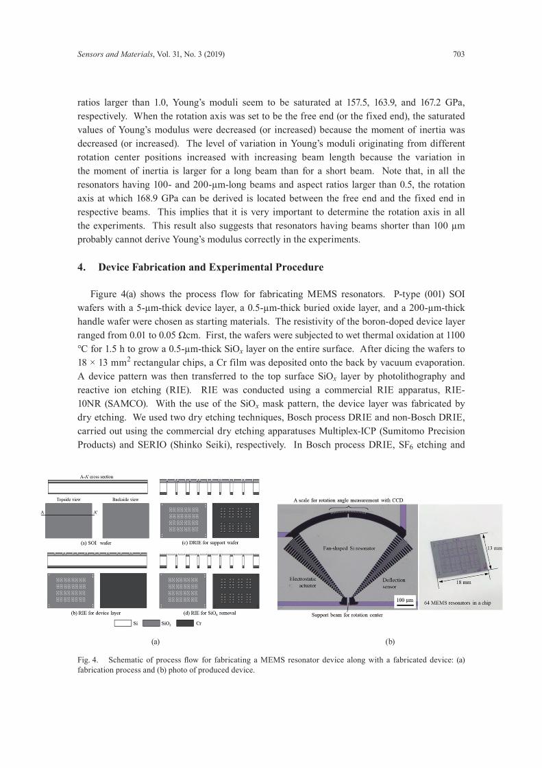
Figure 4(a) shows the process flow for fabricating MEMS resonators. P-type (001) SOI wafers with a 5-µm-thick device layer, a 0.5-µm-thick buried oxide layer, and a 200-µm-thick handle wafer were chosen as starting materials. The resistivity of the boron-doped device layer ranged from 0.01 to 0.05 Ωcm. First, the wafers were subjected to wet thermal oxidation at 1100 ℃ for 1.5 h to grow a 0.5-µm-thick SiOx layer on the entire surface. After dicing the wafers to 18 × 13 mm2 rectangular chips, a Cr film was deposited onto the back by vacuum evaporation. A device pattern was then transferred to the top surface SiOx layer by photolithography and reactive ion etching (RIE). RIE was conducted using a commercial RIE apparatus, RIE-10NR (SAMCO). With the use of the SiOx mask pattern, the device layer was fabricated by dry etching. We used two dry etching techniques, Bosch process DRIE and non-Bosch DRIE, carried out using the commercial dry etching apparatuses Multiplex-ICP (Sumitomo Precision Products) and SERIO (Shinko Seiki), respectively. In Bosch process DRIE, SF6 etching and
(a) (b)
Fig. 4. Schematic of process flow for fabricating a MEMS resonator device along with a fabricated device: (a) fabrication process and (b) photo of produced device.

704 Sensors and Materials, Vol. 31, No. 3 (2019)
C4H8 deposition were repeated five times. That is, the etched depth per SF6 etching process was set to be approximately 1 µm. In the non-Bosch process, O2 and SF6 flow rates were set to be 52 and 92 ml/min, respectively. After device layer etching, a through-hole pattern was fabricated on the back Cr and SiOx layers that were used as the etching mask. The handle wafer was etched by Bosch process DRIE from the back. The SiOx layers remaining over the entire surface were finally removed by RIE. A representative MEMS resonator fabricated by Bosch process DRIE is shown in Fig. 4(b). In total, 64 resonators with support beams of different shapes and sizes were included in a chip. The in-plane pattern was finely formed regardless of the dry etching procedure. To examine the effect of sidewall shape on the derivation of Young’s modulus, we adopted three different sidewall fabrication processes: Bosch process DRIE, non-Bosch DRIE, and FIB etching. These are respectively shown in Figs. 5(a)–5(c) as field-emission scanning electron microscopy (FE-SEM; S4800, Hitachi High-Technologies Corporation) images. FIB etching, which was conducted using a commercial FIB apparatus (FB2200, Hitachi High-Technologies Corporation), was applied to the resonators fabricated by Bosch process DRIE. In Fig. 5(a), a scallop pattern
Fig. 5. SEM images of SCS beam structures fabricated by (a) Bosch process DRIE, (b) non-Bosch process DRIE, and (c) FIB etching after Bosch process DRIE.

Sensors and Materials, Vol. 31, No. 3 (2019) 705
can be seen on the sidewall of the support beam fabricated by Bosch process DRIE. The peak-to-valley distance measured using an atomic force microscope (AFM; SPI4000, Seiko Instruments) was around 0.25 µm. The scallop pattern was uniformly produced on the sidewall of all the Bosch-DRIE structures. In Fig. 5(b), no scallop pattern is seen, but it is found that there are many small vertical lines on the sidewall. The line pattern was probably caused by imperfections of the photolithography process. The endurance of the edge of the photoresist mask pattern was somewhat weak, so that the SiOx mask pattern edge was not finely formed; consequently, a vertical zigzag pattern would have been transferred onto the sidewall of the device layer. The peak-to-valley distance was estimated to be smaller than 0.1 µm. In Fig. 5(c), the sidewall etched with a 40 kV Ga ion beam is found to be very smooth compared with the other two sidewalls. The sidewall roughness might be comparable to that of a polished surface on a SCS wafer. Resonance experiments were implemented using commercial test equipment: a high-speed bipolar amplifier (BA4825, NF Corporation), a frequency response analyzer (FRA5022, NF Corporation), a digital microscope (VHX-1000, KEYENCE), and a manual microprober (K-160MP, Kyowa Riken). Driving voltages ranging from 20 to 40 Vpp with sinusoidal waveform were applied to electrodes on device chips via microprobes. During operation, the phase and amplitude signals from a capacitive sensor were recorded for each test. Resonant frequency was derived from the phase curve peak position that was determined by Lorenz function fitting. All the tests were carried out at ambient temperature in laboratory air.
5. Experimental Results and Discussion
Figure 6 shows the relationship between the aspect ratio of the support beam and the resonant frequency of the resonators. The triangles, squares, and circles indicate resonant
Fig. 6. Relationship between aspect ratio of support beam and in-plane resonant frequency. The solid lines show the relationships obtained from FE analyses. Experimentally obtained data are plotted approximately on FE analysis lines.

706 Sensors and Materials, Vol. 31, No. 3 (2019)
frequencies of the resonators fabricated by Bosch DRIE, non-Bosch DRIE, and Bosch DRIE plus FIB, respectively. Hereafter, these resonators are named the B-DRIE resonator, NB-DRIE resonator, and DRIE-FIB resonator, respectively. The difference in plot color indicates the difference in the length of the beam; that is, the white, light gray, dark gray, and black plots indicate 25, 50, 75, and 100 µm, respectively. In the NB-DRIE and DRIE-FIB resonators, the relationships between the aspect ratio and the resonant frequency for each support beam length were hyperbolic curves, indicating that the resonant frequencies were decreased monotonically with increasing aspect ratio. The resonant frequencies of these resonators seem to be plotted onto or close to the solid lines that indicate the aspect ratio–frequency relationships derived from FE analyses. However, several plots for the B-DRIE resonators were located slightly far from the FE analysis lines because the FE analysis lines were estimated under the assumption that all the resonators have ideal shapes and dimensions without scallops. Figure 7 shows the relationship between the aspect ratio and Young’s modulus. The experimental Young’s moduli were determined by substituting measured resonant frequencies and measured dimensions into Eq. (7). The explanation of plots in this figure is the same as that in Fig. 6. In the NB-DRIE and DRIE-FIB resonators, when the aspect ratio was in the range from 0.3 to 0.6, Young’s modulus scattered within the range from 105.2 to 149.8 GPa. They are 23.7–4.3% lower than the FE analysis values, represented as the solid lines. The difference between the measured Young’s moduli and the FE analysis values are probably associated with the difference between the device’s actual shape and the FE model’s ideal shape. Moreover, these measured values are −37.7 to 11.3% of the ideal value, 168.9 GPa. With increasing aspect ratio, data scatter was reduced, and also, Young’s moduli gradually increased. For example, Young’s modulus of 155 GPa at the aspect ratio of 1.0 increased to 162 GPa on average with the increase in the aspect ratio to 1.6. As the ratio increased further, the ratio–modulus curve
Fig. 7. Relationship between aspect ratio of support beam and Young’s modulus. The difference percentage between FEA Young’s modulus and ideal value is also plotted. Young’s modulus data obtained from non-Bosch-DRIE and FIB-etched resonators show an increasing trend to 168.9 GPa with increasing aspect ratio, as do FE analysis data. In contrast, the data from Bosch-DRIE resonators are different.
Sensors and Materials, Vol. 31, No. 3 (2019) 707
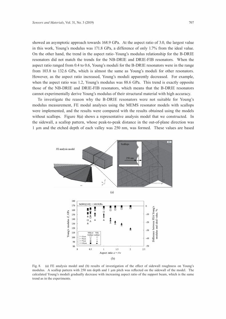
showed an asymptotic approach towards 168.9 GPa. At the aspect ratio of 3.0, the largest value in this work, Young’s modulus was 171.8 GPa, a difference of only 1.7% from the ideal value. On the other hand, the trend in the aspect ratio–Young’s modulus relationship for the B-DRIE resonators did not match the trends for the NB-DRIE and DRIE-FIB resonators. When the aspect ratio ranged from 0.4 to 0.6, Young’s moduli for the B-DRIE resonators were in the range from 103.8 to 132.6 GPa, which is almost the same as Young’s moduli for other resonators. However, as the aspect ratio increased, Young’s moduli apparently decreased. For example, when the aspect ratio was 1.2, Young’s modulus was 88.6 GPa. This trend is exactly opposite those of the NB-DRIE and DRIE-FIB resonators, which means that the B-DRIE resonators cannot experimentally derive Young’s modulus of their structural material with high accuracy. To investigate the reason why the B-DRIE resonators were not suitable for Young’s modulus measurement, FE modal analyses using the MEMS resonator models with scallops were implemented, and the results were compared with the results obtained using the models without scallops. Figure 8(a) shows a representative analysis model that we constructed. In the sidewall, a scallop pattern, whose peak-to-peak distance in the out-of-plane direction was 1 µm and the etched depth of each valley was 250 nm, was formed. These values are based
(a)
(b)
Fig. 8. (a) FE analysis model and (b) results of investigation of the effect of sidewall roughness on Young’s modulus. A scallop pattern with 250 nm depth and 1 µm pitch was reflected on the sidewall of the model. The calculated Young’s moduli gradually decrease with increasing aspect ratio of the support beam, which is the same trend as in the experiments.
708 Sensors and Materials, Vol. 31, No. 3 (2019)
on the AFM and FE-SEM observation results, although the AFM images are not presented here (the FE-SEM images are shown in Fig. 5). Figure 8(b) shows the FE modal analysis results revealing the relationship between the aspect ratio and Young’s modulus. The triangles and squares indicate the results obtained using device models with and without scallops, respectively. The white, light-gray, dark-gray, and black plots indicate the results obtained using 25-, 50-, 75-, and 100-µm-long support beam devices, respectively. The calculated Young’s moduli for the models with scallops at the aspect ratio of 0.4 were 130.8–154.9 GPa, which are approximately 5% lower than those for the models without scallops. In the aspect ratio ranging from 0.4 to 0.7, the moduli of the scallop models steadily increased with increasing ratio, as with the scallop-free models. For example, at the ratio of 0.7, the moduli were 138.1–153.4 GPa, indicating an approximately 5% increase from those at the ratio of 0.4. However, in the region where the aspect ratios were larger than 0.7, the moduli started to decrease monotonically. This trend is diametrically opposite to the results for the scallop-free models. This phenomenon is presumably related to the ratio of the etched depth in the scallop sidewall to the support beam width. When the aspect ratio is 1.0 (beam width is 5.0 µm), the ratio of the etched depth to the beam width is calculated to be 10%. From this ratio, a negative effect of the scallops on Young’s modulus starts to appear. As the aspect ratio (beam width) increased to 2.0 (2.5 µm), Young’s modulus linearly decreased to 118 GPa, which is an approximately 16% decrease from the modulus at the ratio of 1.0 (5 µm). The stiffness of the support beam to the in-plane bending motion is definitely reduced with a decrease in the beam width.(33,36) In the B-DRIE resonators, the stiffness is more reduced owing to the existence of the scallops. The reduction ratio definitely increases with decreasing beam width because the etched depth in the scallops is constant in all the resonators owing to the use of the common Bosch process recipe. Therefore, a substantial reduction in the beam stiffness leads to a large reduction in the resonant frequency, which would have resulted in the decrease in Young’s modulus with increasing ratio. When using MEMS resonators, one possible requirement for accurately deriving the Young’s modulus of a structural material is to reduce the number of scallops and other irregularities on the sidewall as much as possible. Figures 9(a) and 9(b) show the support beam length effect and beam aspect ratio effect, respectively, determined from the experiments using resonators with a smooth sidewall. The squares and circles indicate the results obtained using the NB-DRIE and DRIE-FIB resonators, respectively. The definition of plot color is different in the two graphs; in Fig. 9(a), the white, light-gray, dark-gray, and black plots are for 25-, 50-, 75-, and 100-µm-long beam resonators, whereas in Fig. 9(b), these colored plots indicate the ranges of beam aspect ratios, 0 < a < 0.5, 0.5 ≤ a < 1.0, 1 ≤ a < 1.5, and 1.5 ≤ a, respectively. In each graph, almost all the plots are found to be below the diagonal, which indicates that Young’s moduli obtained in the experiments are lower than those obtained in the FE analyses. This might be associated with the resolution and accuracy of frequency and dimension measurement techniques, except for the sidewall effect discussed in Fig. 8. The FE analyses results in Fig. 9(a) show that the NB-DRIE resonators with a long support beam have the potential to derive a high Young’s modulus. However, although a 50-µm-long support beam was the longest in the NB-DRIE resonators, the experimentally obtained Young’s moduli were, at most, about 13% lower than the FE analyses results. In

Sensors and Materials, Vol. 31, No. 3 (2019) 709
the DRIE-FIB resonators, Young’s moduli were 145–172 GPa, which are closer to the ideal value than the values for the NB-DRIE resonators. Although the results for the DRIE-FIB resonators show that there is only a slight support beam length effect, to accurately measure Young’s modulus, it is important to use resonators with a long support beam and a flat sidewall. In Fig. 9(b), it is seen that the resonators with a support beam with a large aspect ratio could provide a high Young’s modulus. In DRIE-FIB resonators with a 100-µm-long support beam, when the aspect ratio was larger than 1.5, Young’s moduli ranged from 153.0 to 172.7 GPa, which are close to the ideal value. A support beam with a large aspect ratio is indispensable to accurately measure Young’s modulus, in addition to a long support beam and a flat sidewall. However, even under the best conditions of a beam length of 100 µm, an aspect ratio larger than 1.5, and a flat sidewall due to FIB fabrication, the obtained data included a maximum deviation of approximately 9% from the ideal value. This might be caused by FIB-induced surface damage on the sidewall. In the case of FIB fabrication at 40 keV, a gallium-included amorphous silicon layer is known to be formed on the fabricated surface.(37–39) Young’s modulus of the damaged layer is assumed to be 80–110 GPa,(40–42) which reduces the apparent Young’s modulus of the whole support beam. Although the layer thickness is estimated to be only 25–40 nm,(43–45) the amorphous layer possibly provides a negative effect on Young’s modulus. Therefore, in addition to the above-described conditions, reducing any fabrication damage on the sidewall would be significant for increasing the accuracy of the measurement of Young’s modulus of a structural material.
(a) (b)
Fig. 9. Effects of (a) support beam length and (b) support beam aspect ratio on Young’s modulus of resonator. It is found that Young’s moduli of the produced resonators are experimentally measured with high accuracy if the resonators that can show Young’s moduli close to the ideal value in FE analyses are fabricated by non-Bosch DRIE or FIB etching.

710 Sensors and Materials, Vol. 31, No. 3 (2019)
6. Conclusions
For the simple and accurate measurement of Young’s modulus from resonant frequency, we designed and fabricated in-plane-motion SCS MEMS resonators. FE analyses were used to determine the best dimensions of the resonators for Young’s modulus measurement. As a result, the length and aspect ratio of the support beam for a fan-shaped resonator were found to be the most important parameters for the desired purpose. After the structural design using FE analyses, the resonators were fabricated by three different fabrication techniques in order to investigate the effect of the fabrication method on Young’s modulus derivation. Young’s moduli of the NB-DRIE and DRIE-FIB resonators increased to 168.9 GPa with increasing aspect ratio of the support beam, similarly to the FE analyses results, whereas those for the B-DRIE resonators gradually decreased with increasing ratio. FE analyses with scallop beam models showed the same trend as the experiments. By the resonance method, for the simple and accurate measurement of Young’s modulus of a structural material, it was found that resonators with a long support beam, a large aspect ratio of the beam, and a flat sidewall should be prepared and used in the experiments.
Acknowledgments
The authors express their gratitude to Dr. S. Miyake and Mr. T. Kato, Kobelco Research Institute Inc., for extensive discussion on this paper. This work was partly supported by the Grant-in-Aid of the Hyogo COE Program Promotion Project.
References
1 G. T. A. Kovacs: Micromachined Transducers Sourcebook (McGraw-Hill, New York, 1998) p. 586 2 M. A. Haque and M. T. Saif: J. Microelectromech. Syst. 10 (2001) 146. 3 W. Kang and M. T. Saif: J. Microelectromech. Syst. 19 (2010) 1309. 4 W. Kang, J. Han, and M. T. Saif: J. Microelectromech. Syst. 19 (2010) 1322. 5 Y. Zhu, A. Corigliano, and H. D. Espinosa: J. Micromech. Microeng. 16 (2006) 242. 6 M. Kiuchi, S. Matsui, and Y. Isono: J. Microelectromech. Syst. 16 (2007) 191. 7 T. Tsuchiya, Y. Ura, K. Sugano, and O. Tabata: J. Microelectromech. Syst. 21 (2012) 523. 8 S. Johansson, J. A. Schweitz, L. Tenerz, and J. Tiren: J. Appl. Phys. 63 (1988) 4799. 9 C. J. Wilson and P. A. Beck: J. Microelectromech. Syst. 5 (1996) 142. 10 T. Namazu, Y. Isono, and T. Tanaka: J. Microelectromech. Syst. 9 (2000) 450. 11 T. Namazu, Y. Isono, and T. Tanaka: J. Microelectromech. Syst. 1 (2002) 125. 12 X. Ti, T. Ono, Y. Wang, and M. Esashi: Appl. Phys. Lett. 83 (2003) 3081. 13 W. Chang and C. Zorman: J. Mater. Sci. 43 (2008) 4512. 14 M. M. J. Treacy, T. W. Ebbesen, and J. M. Gibson: Nature 381 (1996) 678. 15 L. M. Zhang, D. Uttamchandani, B. Culshaw, and P. Dobson: Meas. Sci. Technol. 1 (1990) 1343. 16 C. L. Muhlstein, E. A, Stach, and R. O. Ritchie: Acta Mater. 50 (2002) 3579. 17 C. L. Muhlstein, R. T. Howe, and R. O. Ritchie: Mech. Mater. 36 (2004) 13. 18 O. N. Pierron, C. C. Abnet, and C. L. Muhlstein: Sens. Actuators, A 128 (2006) 140. 19 D. H. Alsem, C. L. Muhlstein, E. A. Stach, and R. O. Ritchie: Scr. Mater. 59 (2008) 931. 20 W. N. Shape Jr., D. A. LaVan, and R. L. Edwards: Proc. 9th Int. Conf. Solid-State Sensors and Actuators (1997)
607. 21 S. Cho, I. Chasiotis, T. A. Friedmann, and J. P. Sullivan: J. Micromech. Microeng. 15 (2005) 7 28. 22 T. Namazu, S. Inoue, D. Ano, and K. Koterazawa: 17th IEEE Int. Conf. Micro Electro Mechanical Systems (2004)
157.

Sensors and Materials, Vol. 31, No. 3 (2019) 711
23 T. Namazu and S. Inoue: Fatigue Fract. Eng. Mater. Struct. 30 (2007) 13. 24 A. N. Cleland and M. L. Roukes: Appl. Phys. Lett. 69 (1996) 2653. 25 V. Kaajakari, T. Mattila A. Lispin, and A. Oja: Sens. Actuators, A 120 (2004) 64. 26 S. Puchegger, D. Loidl, K. Kromp, H. Peterlik, and R. Weib: J. Sound Vib. 279 (2005) 1121. 27 T. Ikehara and T. Tsuchiya: 21th IEEE Int. Conf. Micro Electro Mechanical Systems (2008) 436. 28 T. Ikehara and T. Tsuchiya: J. Micromech. Microeng. 28 (2008) 075004. 29 C. L. Muhlstein, S. B. Brown, and R. O. Ritchie: Sens. Actuators, A. 94 (2001) 177. 30 C. L. Muhlstein, S. B. Brown, and R. O. Ritchie: J. Microelectromech. Syst. 10 (2001) 593. 31 Y. Uchida, K. Sugano, T. Tsuchiya, O. Tabata, and T. Ikehara: IEEJ Trans. Sens. Micromach. 128 (2008). 32 J. Gasper, V. Chu, and J. P. Conde: J. Appl. Phys. 97 (2005) 094501. 33 B. Llic, S. Krylov, and H. G. Craighead: J. Appl. Phys. 108 (2010) 044317. 34 J. P. Cleveland, S. Manne, D. Bocek, and P. K. Hansma: Rev. Sci. Instrum. 64 (1993) 403. 35 H. J. McSkimin: J. Appl. Phys. 24 (1953) 988. 36 V. P. Adiga, A. V Sumant, S. Suresh, C. Gudeman, O. Auciello, J. A, Carlisle, and R. W. Carpick: Phys. Rev. B
79 (2009) 245403. 37 D. Keiner, C. Motz, M. Rester, M. Jenko, and G. Dehm: Mater. Sci. Eng., A 459 (2007) 262. 38 J. A. El-Awady, C. Woodward, D. M. Dimiduk, and N. M. Ghoniem: Phys. Rev. B 80 (2009) 104104. 39 S.-W. Lee, D. Mordehai, E. Rabkin, and W. D. Nix: J. Mater. Res. 26 (2011) 1653. 40 C. Gaire, D.-X. Ye, F. Tang, R. C. Picu, G.-C. Wang, and T.-M. Lu: J. Nanosci. Nanotech. 5 (2005) 1893. 41 C. L. Allred, X. Yuan, M. Z. Bazant, and L. W. Hobbs: Phys. Rev. B 70 (2004) 134113. 42 L. B. Freund and S. Suresh: Thin Film Materials: Stress, Defect Formation and Surface Evolution (Cambridge
University Press, London, 2003) 96. 43 Z. Wang, T. Kato, T. Hirayama, N. Kato, K. Sasaki, and H. Saka: Appl. Surf. Sci. 241 (2005) 80. 44 N. I. Kato: J. Electron Microscopy 53 (2004) 451. 45 N. I. Kato: J. Vac. Sci. Technol., A 17 (1999) 1201.