Embed Size (px)
Citation preview
Design and performance of the Spider instrument
M. C. Runyana, P.A.R. Adeb, M. Amiric, S. Bentond, R. Biharye, J.J. Bocka,f, J.R. Bondg,J.A. Bonettif, S.A. Bryane, H.C. Chiangh, C.R. Contaldii, B.P. Crilla,f, O. Dorea,f, D. O’Deai,
M. Farhangd, J.P. Filippinia, L. Fisseld, N. Gandilod, S.R. Golwalaa, J.E. Gudmundssonh,M. Hasselfieldc, M. Halpernc, G. Hiltonj, W. Holmesf, V.V. Hristova, K.D. Irwinj, W.C. Jonesh
, C.L. Kuok, C.J. MacTavishl, P.V. Masona, T.A. Morforda, T.E. Montroye, C.B. Netterfieldd,A.S. Rahlinh, C.D. Reintsemaj, J.E. Ruhle, M.C. Runyana, M.A. Schenkera, J. Shariffd,
J.D. Solerd, A. Trangsruda, R.S. Tuckera, C. Tuckerb, and A. Turnerf
aDivision of Physics, Mathematics, and Astronomy, California Institute of Technology,Pasadena, CA, USA;
bSchool of Physics and Astronomy, Cardiff University, Cardiff, UK;cDepartment of Physics and Astronomy, University of British Columbia, Vancouver, BC,
Canada;dDepartment of Physics, University of Toronto, Toronto, ON, Canada;
eDepartment of Physics, Case Western Reserve University, Cleveland, OH, USA;fJet Propulsion Laboratory, Pasadena, CA, USA;
gCanadian Institute for Theoretical Astrophysics, University of Toronto, Toronto, ON, Canada;hDepartment of Physics, Princeton University, Princeton, NJ, USA;
iDepartment of Physics, Imperial College, University of London, London, UK;jNational Institute of Standards and Technology, Boulder, CO, USA;kDepartment of Physics, Stanford University, Stanford, CA, USA;
lKavli Institute for Cosmology, University of Cambridge, Cambridge, UK
ABSTRACT
Here we describe the design and performance of the Spider instrument. Spider is a balloon-borne cosmicmicrowave background polarization imager that will map part of the sky at 90, 145, and 280 GHz with sub-degree resolution and high sensitivity. This paper discusses the general design principles of the instrument inserts,mechanical structures, optics, focal plane architecture, thermal architecture, and magnetic shielding of the TESsensors and SQUID multiplexer. We also describe the optical, noise, and magnetic shielding performance of the145 GHz prototype instrument insert.
Keywords: Spider, cosmic microwave background, polarization, cryogenics, magnetic shielding
1. INTRODUCTION
1.1 The Spider Project
The Spider instrument in a balloon-borne millimeter-wave polarimeter designed to make very high sensitivitymeasurements of the polarization in the cosmic microwave background on mid- to large-angular scales with thegoal of detecting primordial gravity waves from the inflationary epoch of the early universe. Spider will observeat 90, 145, and 280 GHz with beam sizes of 51′, 31′, and 17′, respectively. An Antarctic flight of 24 days willallow Spider to map 8% of the sky to a depth of 0.25, 0.21, and 0.74 µKCMB per square degree at 90, 145, and280 GHz, respectively. A more detailed description of the Spider project can be found in Filippini et al.,1 inthese proceedings, as well as Crill et al.2
arX
iv:1
106.
2173
v1 [
astr
o-ph
.IM
] 1
0 Ju
n 20
11
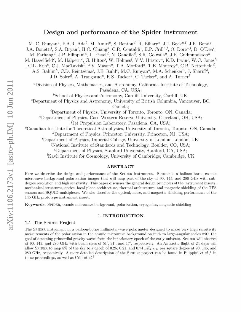
Focal PlaneA4K Spittoon
(1 6K)
Cooled Black Optics Sleeve
4K Filters
Focal Plane (300mK)
(1.6K)p
(1.6K)
Copper-cladG-10 Wrap (4K)
3He Sorption Fridge
G-10 Wrap (4K)
Objective LensObjective Lens (4K)
Optical Stop (1.6K)
Eyepiece Lens (4K)
Metal-mesh Filter (1 6K)
4K Cold Plate Aux Post (1.6K)
Lead Shield (4K)
Filter (1.6K)
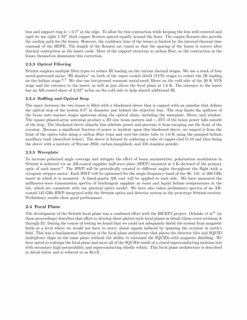
Figure 1. At left: Cross-section of the Spider instrument insert Solidworks model with key components labeled. At right:Photo of the Spider instrument insert without the outermost copper-clad G-10 wrap. Visible in the photo are the carbonfiber trusses, the high-µ magnetic shield called the spittoon, the cooled optics sleeve between the lenses, thermal straps,cables, and the cold plate.
1.2 The Spider Instrument Payload and Cryostat
At the heart of the Spider balloon payload is a large liquid helium cryostat. The cryostat houses up to sixinstrument inserts (described below) bolted to a ∼ 1000` helium tank with all of the inserts pointed in the samedirection. The cryostat cryogenics are briefly described in section 2.5 below and a more thorough discussioncan be found in Gudmundsson et al.3 in this volume. The cryostat measures 2.2 m in length and 2.0 m indiameter. The cryostat is mounted to a carbon fiber gondola via two pillow blocks that allow the cryostat totilt in elevation. The gondola will be suspended from a 8 million cubic foot helium stratospheric balloon and issteerable in both elevation and azimuth. Power to the instrument is provided by solar arrays mounted to theback side of the payload and the instrument always points no closer than 45 deg to the sun.
2. INSTRUMENT INSERTS
2.1 Introduction and Design Considerations
One of the biggest concerns for Spider is instrument payload mass. The science payload lifting capacity of theballoon is limited to ∼ 5000 pounds and the duration of our flight will depend, in part, upon payload mass.To that end we have tried to balance the constraint on mass with the desire to build a stiff structure that willnot deflect under the periodic acceleration of the gondola scan pattern, nor break during launch (and hopefullylanding). Materials with high thermal conductivity (such as copper) and good magnetic shielding properties(niobium, lead, and high-permeability materials) tend to be dense. So we have tried to minimize their use whereever possible. We had the benefit of starting the Spider insert design after much of the design of our sisterexperiment BICEP2 was completed. BICEP2 was designed for operation from the ground where weight is notas serious of a concern. We identified many areas where we could reduce the weight of the insert design witheither a change in materials, strategic light weighting, or completely modifying a component (such as changinglarge metal tubes for carbon fiber trusses sheathed in light-weight copper-clad fiberglass).
2.2 Optics Truss Structure and Cold Plate
A gold-plated 1/2′′ thick ∅17.35′′ 1100-H14 aluminum cold plate forms the base of each Spider insert and is theinterface to which the inserts mount to the cryostat helium tank. This aluminum plate has been light-weighted
significantly. On top of this cold plate is mounted a 3He sorption fridge and the truss structure that supportsthe optics and focal plane. A gold-plated C10100 copper bus bar is mounted to the bottom side of the coldplate and the sorption fridge is bolted to this. The other side of this thermal bus is connected to copper tabsembedded in the liquid helium tank of the cryostat. A gold-plated copper bar penetrates the cold plate; thebottom side is connected to the pumped helium auxiliary tank of the cryostat and the other provides a 1.6 Kpoint for the condensation point of the sorption fridge, a thermal intercept ring in the focal plane unit (FPU),a high-µ magnetic shield, and a cooled blackened light baffle, all of which are described below.
The focal plane unit is supported above the cold plate by a hexapod carbon fiber truss with ∅1/2′′ rods calledthe camera truss. The two lenses are then supported from the top of the camera truss by two octopod carbonfiber trusses with ∅3/8′′ rods. The individual carbon fiber legs have aluminum end caps epoxied to each endwith Stycast 2850 and we have used fishing line to center the carbon fiber rods in the end caps to avoid possiblegalvanic corrosion from electrical contact. The mounting holes in the end caps have all been reamed to have aslip fit tolerance over ∅1/4′′ shoulder bolts. The mounting pads on the feet that mount the rod assemblies tothe aluminum rings are all coplanar for each leg. This allows the length of any truss to be changed simply byswapping out legs of different length. The insert volume in the single-insert test cryostat used for developmentand characterization is longer than that in the flight cryostat and we will compensate by shrinking the length ofeach camera truss by 4′′ before installing the inserts into the flight cryostat.
All of the carbon fiber trusses are wrapped in thin copper-clad G-10 sheets to form a light and RF tight sleevearound the inserts. We have the option of coating the inside of these wraps with a flexible blackening materialmade from silicone RTV, carbon lampblack, and 316 stainless powder. We measured the mass loss during cureand heating of many commercially available silicones and found Dow Corning 748 to have very low mass loss.We have run our cryostat with ∼ 1.5 m2 of this material and had no issues with out gassing. Outside of thewraps run four C10100 copper bars to cool the optics trusses. Each insert is capped with a 1100 aluminum snoutthat holds a set of filters in front of the objective lens. These filters are described in section 2.3.3 below.
2.3 Optics
2.3.1 Design Description
Each Spider insert is a cooled two-lens refracting telescope. The lens design is identical to that of the BICEP2experiment and is described in detail in Aikin et al.4 (in these proceedings). Both sides of the two lenses aresimple conics and are separated by 550 mm with an effective focal length of 583.5 mm. This yields a plate scale of0.98 deg/cm on the focal plane. The optical system is telecentric to accommodate the flat focal plane geometry.The field of view of each insert is 20 deg across the diagonal. The entire telescope optics are cooled to 4.2 K toreduce the in-band loading from loss in the thick dielectric lenses.
2.3.2 Lenses, AR Coats, and Flexures
The lenses used in Spider are machined from 2′′ thick cast HDPE slabs. The lens fabrication process involves anumber of steps designed to reduce the stress in the lens and achieve the desired lens figure. Before machining,the HDPE slabs are annealed in a temperature-controlled oven between metal plates and then rough cut toshape. The rough cut lenses are then clamped in an annealing jig and re-annealed before finish machining on aCNC mill. The finished lenses are then measured on a CMM to assure the lens figure and surface finish have beenarchived. The maximum allowable deviation in the lens figure is 0.005′′ and the lens surface finish is < 63µ′′.The final lenses are 12.4′′ in diameter with an optically-active diameter of 11.4′′.
Because the index of refraction of HDPE in the millimeter is ∼ 1.52,5 the instrument would suffer reflectionsof order [(n1 − n2)/(n1 + n2)]2 ∼ 4% at each lens surface. To reduce these reflections we bond a tuned layerof porous PTFE sheet to each lens surface manufactured by Porex. We have chosen a material with a densitythat yields an index of refraction close to the ideal of nAR =
√nHDPE and we order the sheets in thicknesses of
λ/4nAR. The toleracing of the AR material from the manufacturer is only good to a few mils. But modeling ofthe transimission of HDPE (and nylon) slabs with AR coats of various thickness and indicies of refraction showsthat > 99% transmission is achieved with thickness and density variations within manufacturing tolerances.
The plastic lenses contract during cooling substantially more than the aluminum mounts from which theyare supported (∼ 2% for HDPE and only ∼ 0.4% for aluminum). The radial differential contraction between the
lens and support ring is ∼ 0.1′′ at the edge. To allow for this contraction while keeping the lens well centered andrigid we use eight 1/32′′ thick copper flexures spaced equally around the lenes. The copper flexures also providethe cooling path for the lenses. However, the cooldown time of the lenses is limited by the internal thermal timeconstant of the HDPE. The length of the flexures are tuned so that the spacing of the lenses is correct afterthermal contraction as the insert cools. Most of the support structure is carbon fiber, so the contraction in thelenses themselves dominates this correction.
2.3.3 Optical Filtering
Spider employs multiple filter types to reduce IR loading on the various thermal stages. We use a stack of fourmetal-patterned mylar “IR shaders” on both of the vapor cooled shield (VCS) stages to reduce the IR loadingon the helium stage.6,7 We also use hot-pressed resonant metal-mesh filters on the cold side of the 20 K VCSstage and the entrance to the insert, as well as just above the focal plane at 1.6 K. The entrance to the inserthas an AR-coated sheet of 3/32′′ nylon on the cold side to help absorb additional IR.
2.3.4 Baffling and Optical Stop
The space between the two lenses is filled with a blackened sleeve that is capped with an annulus that definesthe optical stop of the system 9.5′′ in diameter just behind the objective lens. The stop limits the spillover ofthe beam onto warmer stages upstream along the optical chain, including the waveplate, filters, and window.The square phased-array antennas produce a 2D sinc beam pattern and ∼ 25% of the beam power falls outsideof the stop. The blackened sleeve absorbs this sidelobe power and prevents it from escaping out the front of thecryostat. Because a significant fraction of power is incident upon this blackened sleeve, we susped is from thefront of the optics tube using a carbon fiber truss and cool the entire tube to 1.6 K using the pumped heliumauxilliary tank (described below). The sleeve is formed by soldering a tube of copper-clad G-10 and then liningthe sleeve with a mixture of Stycast 2850, carbon lampblack, and 316 stainless powder.
2.3.5 Waveplate
To increase polarized angle coverage and mitigate the effect of beam asymmetries, polarization modulation inSpider is achieved via an AR-coated sapphire half-wave plate (HWP) mounted at 4 K skyward of the primaryoptic of each insert.8 The HWP will be periodically rotated to different angles throughout the flight with acryogenic stepper motor. Each HWP will be optimized for the single frequency band of the 90, 145, or 280 GHzinsert in which it is mounted. A fused-quartz AR coat will be applied to each side. We have measured themillimeter-wave transmission spectra of birefringent sapphire at room and liquid helium temperatures in thelab, which are consistent with our physical optics model. We have also taken preliminary spectra of an AR-coated 145 GHz HWP integrated with the Spider optics and detector system in the prototype Spider receiver.Preliminary results show good performance.
2.4 Focal Plane
The development of the Spider focal plane was a combined effort with the BICEP2 project. Orlando et al.9 (inthese proceedings) describes that effort to develop these platter-style focal planes in detail (these cover revisions Athrough D). During the course of testing we found that we could not adequately shield the system from magneticfields at a level where we would not have to worry about signals induced by spinning the cryostat in earth’sfield. This was a fundamental limitation of the focal plane architecture that places the detector tiles and SQUIDmultiplexer chips on the same plane without the ability to surround the SQUIDs with magnetic shielding. Wehave opted to redesign the focal plane and move all of the SQUIDs inside of a closed superconducting niobium boxwith secondary high-permeability and superconducting shields within. This focal plane architecture is describedin detail below and is referred to as RevX.
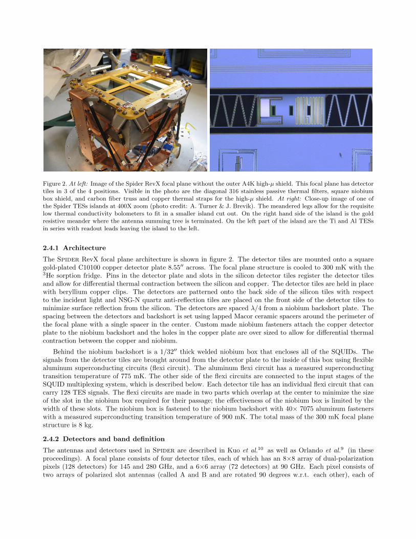
Figure 2. At left: Image of the Spider RevX focal plane without the outer A4K high-µ shield. This focal plane has detectortiles in 3 of the 4 positions. Visible in the photo are the diagonal 316 stainless passive thermal filters, square niobiumbox shield, and carbon fiber truss and copper thermal straps for the high-µ shield. At right: Close-up image of one ofthe Spider TESs islands at 400X zoom (photo credit: A. Turner & J. Brevik). The meandered legs allow for the requisitelow thermal conductivity bolometers to fit in a smaller island cut out. On the right hand side of the island is the goldresistive meander where the antenna summing tree is terminated. On the left part of the island are the Ti and Al TESsin series with readout leads leaving the island to the left.
2.4.1 Architecture
The Spider RevX focal plane architecture is shown in figure 2. The detector tiles are mounted onto a squaregold-plated C10100 copper detector plate 8.55′′ across. The focal plane structure is cooled to 300 mK with the3He sorption fridge. Pins in the detector plate and slots in the silicon detector tiles register the detector tilesand allow for differential thermal contraction between the silicon and copper. The detector tiles are held in placewith beryllium copper clips. The detectors are patterned onto the back side of the silicon tiles with respectto the incident light and NSG-N quartz anti-reflection tiles are placed on the front side of the detector tiles tominimize surface reflection from the silicon. The detectors are spaced λ/4 from a niobium backshort plate. Thespacing between the detectors and backshort is set using lapped Macor ceramic spacers around the perimeter ofthe focal plane with a single spacer in the center. Custom made niobium fasteners attach the copper detectorplate to the niobium backshort and the holes in the copper plate are over sized to allow for differential thermalcontraction between the copper and niobium.
Behind the niobium backshort is a 1/32′′ thick welded niobium box that encloses all of the SQUIDs. Thesignals from the detector tiles are brought around from the detector plate to the inside of this box using flexiblealuminum superconducting circuits (flexi circuit). The aluminum flexi circuit has a measured superconductingtransition temperature of 775 mK. The other side of the flexi circuits are connected to the input stages of theSQUID multiplexing system, which is described below. Each detector tile has an individual flexi circuit that cancarry 128 TES signals. The flexi circuits are made in two parts which overlap at the center to minimize the sizeof the slot in the niobium box required for their passage; the effectiveness of the niobium box is limited by thewidth of these slots. The niobium box is fastened to the niobium backshort with 40× 7075 aluminum fastenerswith a measured superconducting transition temperature of 900 mK. The total mass of the 300 mK focal planestructure is 8 kg.
2.4.2 Detectors and band definition
The antennas and detectors used in Spider are described in Kuo et al.10 as well as Orlando et al.9 (in theseproceedings). A focal plane consists of four detector tiles, each of which has an 8×8 array of dual-polarizationpixels (128 detectors) for 145 and 280 GHz, and a 6×6 array (72 detectors) at 90 GHz. Each pixel consists oftwo arrays of polarized slot antennas (called A and B and are rotated 90 degrees w.r.t. each other), each of
which are summed in phase on superconducting microstrip. This microstrip passes through a resonant filter thatdefines the millimeter-wave frequency band and then the signal is fed into a resistive gold meander located ona suspended bolometer island (see figure 2). Also on each island are both a titanium and aluminum transitionedge sensor (TES) in series. The millimeter power dissipated in the gold meander heats up the bolometer islandand the voltage-biased TES responds to that change in temperature with a change in resistance, thus producinga measurable change in current.
The thermal conductivity (G) of the Spider bolometers is low (20 pW/K at TC) to take advantage of thedecreased optical loading from a stratospheric balloon platform. The G of the bolometers are tuned to put thetitanium TES (TC ∼ 500 mK) on transition at float with a margin of safety of ∼ 3. These low-G devices aresaturated on the titanium transition when doing testing in the laboratory, so the aluminum TES (TC ∼ 1.3 K)in series is used. This allows characterization of beams and frequency bands in the lab before flight. The TESbolometer islands have some response to high-frequency “blue leaks” since the microstrip running to the islandacts like an antenna within the cutout of the niobium ground plane. In an effort to push that frequency responseabove our filter cutoff we have shrunk the window cutout of the islands. The lower Gs of the Spider devicesrequired that the island legs that determine the device G be meandered to obtain enough length for the requiredthermal conductivity.
2.4.3 SQUID multiplexer and cabling
At the heart of Spider’s signal readout chain is a three-stage SQUID time-domain multiplexer made by NIST.11
SQUIDs are remarkably sensitive to changes in magnetic flux, so coupling an input coil into a SQUID loop formsthe basis of a very sensitive current readout. Each bolometer signal is fed through a low-pass L/R filter thatreduces aliased noise and then into the input coil of a clover leaf SQUID (SQ1). A single mux chip handles thesignals from 32 TESs and a “dark” SQUID (used to monitor noise and magnetic field pickup) and combinesthese signals into a summing coil that is fed into a second stage SQUID (SQ2). The individual SQ1 are biasedin sequence, so the summing coil (and hence, SQ2) only has the signal from one of the TESs at any time. TheSQ1 bias lines are referred to as “row selects” because they select which SQ1 is active. The SQ2 signal is thenfed into a SQUID series array amplifier (SSA) that has 100 SQUIDs in series per channel. The timing, biasing,and readout of the SQUIDs is controlled by the Multi-Channel Electronics (MCE) crate made by UBC.12 EachMCE crate handles the 512 detector signals from an entire insert with only a power cable and fiber optic pairleaving the crate.
As mentioned above, the signals from the detectors are routed to the SQUID chips on superconducting flexiblecircuits. The multiplexer chips are mounted on circuit boards with copper traces onto which superconductingPbSn solder has been electroplated between the mux chips and the bond edge. Each of these “MUX boards”has four sets of SQUID chips which are enough to handle the signals from one detector tile (up to 128 devices).The typical impedance of the TESs on the titanium transition is ∼ 30− 40 mΩ and the TES bias shunt resistorsare only 3 mΩ. The superconducting aluminum and PbSn circuit between the TESs and mux chips reduce theparasitic impedance along this path to a level well below the shunt resistance.
The signals from the SQ2s, SQ1 row select lines, detector biases, and SQUID feedback lines are feed to Samtecheaders at the edge of the MUX boards and the four MUX boards plug into one breakout board which routesthe signals to four 100-way micro-D connectors. All of the outputs of the SQ2s are run through one of these100-way connectors up to a separate circuit board that houses the two SSA modules. The other three 100-wayconnectors have all of the signals, biases, and feedback lines and run to the cold plate on NbTi ribbon cables.There are 300 wires leaving the focal plane and the detector bias and SQ2 bias lines can carry currents up to acouple mA each. The joule power dissipation by manganin cables would have been too much for our 3He fridgeto handle. So we have chosen to make all of the wires running to the focal plane superconducting (with theexception of some thermometry). The cables running from the 4 K cold plate to the 300 K vacuum feedthroughto the MCE crate are all teflon-jacketed shielded twisted-pair manganin.
2.4.4 Magnetic shielding
A serious concern to the Spider project is magnetic field pickup in the system that cannot be separated fromastrophysical signals. One of the strengths of the Spider instrument is the ability to make long scans across
A4K spittoon Copper A4K spittoon (1.6K)
Small slots for flexi circuits
Niobium backshort
ppdetector plate
e c cu tsA4K “clean up” plate
A4K sleeves
Aluminum inner shield
Niobium box around SQUID mux chips
SSA Modules (Nb with
Aluminum flexi circuit (Nb with
Metglas wrap)flexi circuit
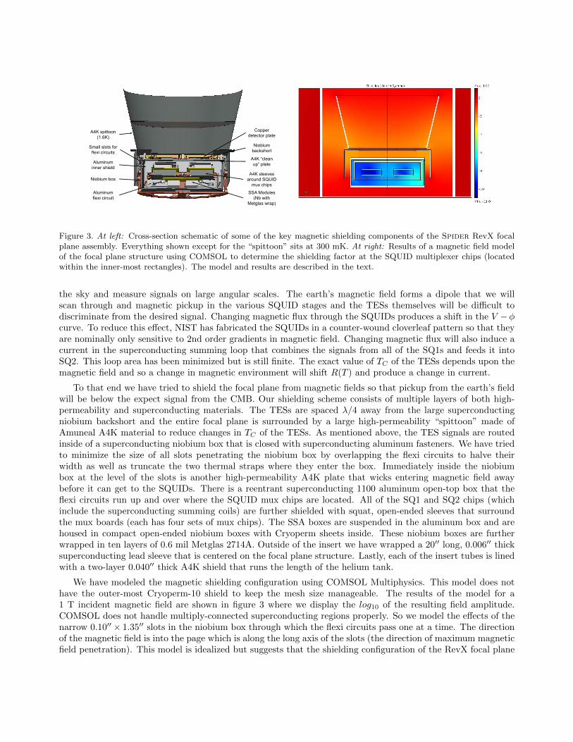
Figure 3. At left: Cross-section schematic of some of the key magnetic shielding components of the Spider RevX focalplane assembly. Everything shown except for the “spittoon” sits at 300 mK. At right: Results of a magnetic field modelof the focal plane structure using COMSOL to determine the shielding factor at the SQUID multiplexer chips (locatedwithin the inner-most rectangles). The model and results are described in the text.
the sky and measure signals on large angular scales. The earth’s magnetic field forms a dipole that we willscan through and magnetic pickup in the various SQUID stages and the TESs themselves will be difficult todiscriminate from the desired signal. Changing magnetic flux through the SQUIDs produces a shift in the V −φcurve. To reduce this effect, NIST has fabricated the SQUIDs in a counter-wound cloverleaf pattern so that theyare nominally only sensitive to 2nd order gradients in magnetic field. Changing magnetic flux will also induce acurrent in the superconducting summing loop that combines the signals from all of the SQ1s and feeds it intoSQ2. This loop area has been minimized but is still finite. The exact value of TC of the TESs depends upon themagnetic field and so a change in magnetic environment will shift R(T ) and produce a change in current.
To that end we have tried to shield the focal plane from magnetic fields so that pickup from the earth’s fieldwill be below the expect signal from the CMB. Our shielding scheme consists of multiple layers of both high-permeability and superconducting materials. The TESs are spaced λ/4 away from the large superconductingniobium backshort and the entire focal plane is surrounded by a large high-permeability “spittoon” made ofAmuneal A4K material to reduce changes in TC of the TESs. As mentioned above, the TES signals are routedinside of a superconducting niobium box that is closed with superconducting aluminum fasteners. We have triedto minimize the size of all slots penetrating the niobium box by overlapping the flexi circuits to halve theirwidth as well as truncate the two thermal straps where they enter the box. Immediately inside the niobiumbox at the level of the slots is another high-permeability A4K plate that wicks entering magnetic field awaybefore it can get to the SQUIDs. There is a reentrant superconducting 1100 aluminum open-top box that theflexi circuits run up and over where the SQUID mux chips are located. All of the SQ1 and SQ2 chips (whichinclude the superconducting summing coils) are further shielded with squat, open-ended sleeves that surroundthe mux boards (each has four sets of mux chips). The SSA boxes are suspended in the aluminum box and arehoused in compact open-ended niobium boxes with Cryoperm sheets inside. These niobium boxes are furtherwrapped in ten layers of 0.6 mil Metglas 2714A. Outside of the insert we have wrapped a 20′′ long, 0.006′′ thicksuperconducting lead sleeve that is centered on the focal plane structure. Lastly, each of the insert tubes is linedwith a two-layer 0.040′′ thick A4K shield that runs the length of the helium tank.
We have modeled the magnetic shielding configuration using COMSOL Multiphysics. This model does nothave the outer-most Cryoperm-10 shield to keep the mesh size manageable. The results of the model for a1 T incident magnetic field are shown in figure 3 where we display the log10 of the resulting field amplitude.COMSOL does not handle multiply-connected superconducting regions properly. So we model the effects of thenarrow 0.10′′ × 1.35′′ slots in the niobium box through which the flexi circuits pass one at a time. The directionof the magnetic field is into the page which is along the long axis of the slots (the direction of maximum magneticfield penetration). This model is idealized but suggests that the shielding configuration of the RevX focal plane
is capable of yielding shielding factors in excess of 108 at the SQUIDs, not including the additional A4K tubesthat run the length of the helium tank and are expected to provide an additional shielding factor of ∼ 50. Wehave estimated the shielding factor to earth’s magnetic field necessary for the flight to be ∼ 107.
2.5 Cryogenics
2.5.1 Overview
The Spider Long Duration Balloon (LDB) cryostat and cryogenic systems are described in detail in Gudmunds-son et al.3 (in these proceedings). The cryostat holds ∼ 1000` of liquid helium in a tank shaped like a 6-shotrevolver cylinder. There are seven holes in the tank; the six around the outside house the six instrument insertsand the central hole is used to pass wiring up to the waveplates and thermometry in front of the inserts. Thesix instrument cold plates (described above) bolt to the liquid helium tank via gold-plated aluminum interfaceplates. In addition to the main helium tank, a smaller 20` auxiliary tank (Aux tank) of helium is fed via acapillary tube from the main tank and is pumped to 1.6 K. On the ground, this pumping is achieved with avacuum pump but in flight the reduced atmospheric pressure at float provides the pumping. As described below,the Aux tank provides an intermediate temperature stage between our sub-K fridge and the main liquid heliumbath.
2.5.2 Truss structure and thermal management
The focal plane unit (FPU) is supported on eight 316 stainless “heat capacity blocks”. The cooling path from theFPU to the 3He fridge still runs through these blocks and we have measured them to have a combined thermalimpedance of 2.3 mK/µW, in excellent agreement with COMSOL simulations. They are gold plated on the endsto minimize thermal boundary impedance. Stainless steel has a relatively high heat capacity and these blocksact as a passive thermal filter to temperature fluctuations generated below in the truss structure, thermal straps,or the fridge. We have measured the thermal transfer function of the passive thermal filter to have a 3dB pointof 2 mHz.
The heat capacity blocks connect the four sides of the FPU to a copper ring via copper supports. This wholestructure is cooled to 300 mK and is referred to as the sub-Kelvin stage (sub-K stage). The sub-K stage issupported off of another copper ring cooled to 1.6 K with the pumped helium auxiliary tank with carbon fiberrods. This “aux ring” is itself supported from a 4.2 K aluminum ring with carbon fiber rods. We measuredthe thermal conductivity of many polymeric and composite materials during the course of the development ofthe Spider truss structure and found carbon fiber rods to have the highest ratio of elastic modulus to thermalconductivity of non-brittle materials over the range of temperatures of interest.13 The truss structure appearsgossamer but is very stiff. We have modeled the deflection with COMSOL and expect the 8 kg focal plane todeflect a few mils over a 90 deg tilt, corresponding to much less than an arcminute of beam deflection on the sky.
There is a concern that the vibration of rigid metal thermal straps attached to the cold stages might vibrateat frequencies within the science band and couple power into the detectors. The stainless heat capacity blocksdescribed above are part of the strategy to mitigate that effect. We have opted instead to use flexible thermalstraps formed with many layers of 0.001′′ C11000 copper foil that have been electron beam welded into coppermounting tabs. Despite the foil alloy being C11000, we have measured its RRR to be ∼ 200 and confirmed thatthey have correspondingly high thermal conductivity.
We use a combination of DT-series silicon diodes and Cernox resistance thermometers (both made byLakeshore Cryotronics) to monitor the temperatures within the cryostat and inserts. We exclusively use re-sistance thermometers at all sub-K stages and diodes for all stages with temperatures greater than 1 K.
3. Spider SYSTEM PERFORMANCE
3.1 Optical Performance
Spider will observe in three frequency bands at 90, 145, and 280 GHz. Most of the insert development efforthas focused on the 145 GHz system, and consequently, it is the most well characterized of our frequencies. Herewe present some of the optical performance results from the 145 GHz system.
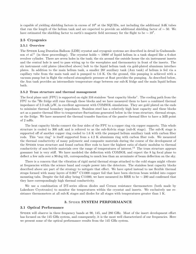
Figure 4. Measured signal bands from three 145 GHz pixel pairs with high S/N. The red and blue curves show the bandsfor each of the two antennas in a pixel pair and the green curve is the difference between the two. The bands have beennormalized to have the same integrated value.
3.1.1 Bands
As mentioned above, Spider’s frequency bands are defined with resonant on-tile filters between the detectorantenna and the resistive meander on the TES island.10 We have measured the spectal response of one of theinserts configured for 145 GHz operation. The average bandwidth for the 145 GHz channels is 34 GHz (using theconvention of Runyan et al.14), or 25%. Even at float we are concerned about residual atmospheric emission andhave worked to fit the frequency bands within the available atmospheric windows, paying particular attention toavoiding water lines.
Spider’s observing strategy will involve differencing the two polarizations in a given pixel and a mismatchin spectra could limit the effectiveness of this strategy. Figure 4 shows examples of measured spectral bands at145 GHz. In the figure, the spectral bands have been normalized to have the same integrated value over the band.The oscillatory nature of the difference band suggests that common mode emission sources with smoothly-varyingspectra will be well-differenced. The Spider filter strategy also effectively removes high-frequency spectral leaksthat could couple high-frequency power onto the detectors. We have measured the high-frequency response ofour 145 GHz band using a chopped thermal source and a thick-grill filter with a cut off of 185 GHz and foundthe response to be less than a few tenths of a percent of the in-band signal (consistent with the noise floor of themeasurement).
3.1.2 Optical efficiency
We needed a way to characterize the Spider instrument inserts under flight-like loading conditions. To do thiswe developed a helium cold load cryostat that bolts to the front of either the insert test cryostat or the flightcryostat and presents a cold, millimeter-black, beam-filling surface to the instrument. This cold load cryostat isa 23` helium cryostat with a 15.5′′ cold plate. Using a carbon fiber truss, we stand off a copper plate coveredin millimeter-black pyramidal tiles manufactured by Thomas Keating, Ltd. Embedded within these tiles aremultiple Lakeshore SD diodes to monitor the load temperature. We have mounted a resistive heater on the backside of the black load and can elevate it to any temperature above 5 K. The cold load cryostat has radiationshields attached to the helium bath and its vapor cooled shield and we have mounted IR-blocking filters to eachof these stages to reduce the optical loading on the black absorber.
A convenient feature of being able to elevate the cold load temperature is that we can measure the end-to-endoptical efficiency of our system by measuring the optical loading on the detectors, Popt, as a function of coldload temperature, TCL. The only optical element missing in this configuration is the cryostat vacuum window(the cold load and main cryostats share a common vacuum) and we have added a handful of IR filters on thecold load side which will not be there in flight. We ramp the cold load temperature from 5 K to ∼ 20 K andtake load curves to measure the loading at each temperature. We convert the actual cold load temperature intoan equivalent Rayleigh-Jeans temperature, TRJ , and then take the slope dPopt/dTRJ = k
∫ην dν, where k is
Boltzmann’s constant, ην is the measured spectral response normalized by the optical efficiency, and we have
assumed single-moded performance (AΩ = λ2). We measure dPopt/dTRJ to be ∼ 0.17 pW/KRJ at 145 GHz.We can then calculate a band-average optical efficiency η = (
∫ην dν)/∆ν. The 145 GHz Spider inserts have a
typical end-to-end optical efficiency of 36%.
3.1.3 Internal loading
To fully take advantage of the stratospheric balloon platform we need to reduce the internal loading to a levelwhere the additional photon noise contribution does not significantly increase the overall system noise. We haveestimated the loading from the CMB and atmosphere at float to be ∼ 0.28 pW per polarization at 145 GHz. Thiscorresponds to a RJ temperature of ∼ 1.7 K for a system with 36% optical efficiency and a 34 GHz bandwidth.The loading from a 300 K vacuum window with 0.5% loss is ∼ 0.2 pW. So we would like the loading from withinthe cryostat to be a small fraction of a pW, or only a few KRJ .
The cold load provides a convenient way to measure the internal loading from within the cryostat. Weextrapolate the Popt versus TRJ curve described in the previous section back to zero and read off the internalloading as the y-intercept. Note that this technique does not include the loading from the warm vacuumwindow, which is estimated to be ∼ 0.25 pW. Before installing the cooled black optics sleeve between the lenseswe measured the internal loading from within the cryostat to be ∼ 0.6 pW, or ∼ 3.5 KRJ at 145 GHz. We havesince installed the cooled optics sleeve and by measuring the coupling of the detectors to the sleeve we expectthe internal loading to decrease by 0.3 to 0.4 pW.
3.1.4 Beams
We have also done some preliminary beam characterization at 145 GHz by looking into the laboratory througha 6′′ thick Zotefoam PPA-30 window (this will not be the flight window configuration). We have made near-fieldbeam maps a few inches away from the window aperture using a chopped thermal source on an X-Y translationstage as well as far-field slices using a large chopped thermal source on a linear stage that can be rotated aboutthe bore sight. The near field beam maps are in qualitative agreement with physical optics modeling usingZemax and the far-field beam slices for the few pixels measured show well-matched gaussian beam pairs for thetwo polarization antennae within a pixel with a FWHM of 31′ at 145 GHz. The difference in the A and Bpolarizations within an individual pixel are measured to be < 2% of the average beam. See Aikin et al.4 in theseproceedings for more details on beams from the BICEP2 optical system, which is very similar to Spider’s.
3.2 Detector performance
We have measured detector parameters for a handful of prototype detector tiles. The Spider-specific engineeringtiles have two different values of G so that we can determine the optimum value for the flight.
3.2.1 Noise
We have measured the instrument noise at 145 GHz versus R/Rn on the TES transition while staring into thecold load cryostat at 5.5 K to simulate flight loading. We calibrate the noise using bolometer load curves and themeasured optical efficiency of the system, dP/dTRJ , and then convert the noise PSDs into NETCMB . We alsoconfirm this calibration by varying the temperature of the blackened cold load plate and measure the responseon the detectors. Some example noise spectra from an A/B pixel pair (as well as the difference PSD) is shownin figure 5.
The angular scales on which Spider will be able to measure the CMB power spectrum will be affected by thecombination of scan speed and 1/f -noise. We have measured the 1/f -knee frequency of undifferenced bolometersto be typically 0.1 to 0.4 Hz. Taking the difference of the two detectors in an A/B pixel pair removes the commonoptical and electrical components and lowers the 1/f frequency to ∼ 60 mHz. This corresponds to ` of a few forthe likely scan speeds of Spider. As seen in the figure, pixel pair differencing produces three decades of cleansignal bandwidth.
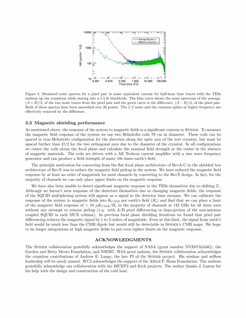
Figure 5. Measured noise spectra for a pixel pair in noise equivalent current for half-hour time traces with the TESsmidway up the transition while staring into a 5.5 K blackbody. The blue curve shows the noise spectrum of the average,(A+B)/2, of the two noise traces from the pixel pair and the green curve is the difference, (A−B)/2, of the pixel pair.Both of these spectra have been smoothed over 20 points. The 1/f noise and the common spikes at higher frequency areeffectively removed by the difference.
3.3 Magnetic shielding performance
As mentioned above, the response of the system to magnetic fields is a significant concern to Spider. To measurethe magnetic field response of the system we use two Helmholtz coils 79 cm in diameter. These coils can bespaced in true Helmholtz configuration for the direction along the optic axis of the test cryostat, but must bespaced further than D/2 for the two orthogonal axes due to the diameter of the cryostat. In all configurationswe center the coils about the focal plane and calculate the nominal field strength at the center in the absenceof magnetic materials. The coils are driven with a AE Techron current amplifier with a sine wave frequencygenerator and can produce a field strength of many 10s times earth’s field.
The principle motivation for converting from the flat focal plane architecture of RevA-C to the shielded boxarchitecture of RevX was to reduce the magnetic field pickup in the system. We have reduced the magnetic fieldresponse by at least an order of magnitude for most channels by converting to the RevX design. In fact, for themajority of channels we can only place upper limits on the magnetic response.
We have also been unable to detect significant magnetic response in the TESs themselves due to shifting Tc.Although we haven’t seen response of the detectors themselves due to changing magnetic fields, the responseof the SQUID multiplexing system will appear as a signal in the detector time streams. We can calibrate theresponse of the system to magnetic fields into KCMB per earth’s field (Be) and find that we can place a limitof the magnetic field response of < 10 µKCMB/Be in the majority of channels at 145 GHz for all three axeswithout any attempt to remove pickup (e.g. with A/B pixel differencing or deprojection of the non-antennacoupled SQUID in each MUX column). In previous focal plane shielding iterations we found that pixel pairdifferencing reduces the magnetic signal by 1 to 2 orders of magnitude. Even at this limit, the signal from earth’sfield would be much less than the CMB dipole but would still be detectable in Spider’s CMB maps. We hopeto do longer integrations at high magnetic fields to put even tighter limits on the magnetic response.
ACKNOWLEDGMENTS
The Spider collaboration gratefully acknowledges the support of NASA (grant number NNX07AL64G), theGordon and Betty Moore Foundation, and NSERC. With great sadness, the Spider collaboration acknowledgesthe countless contributions of Andrew E. Lange, the late PI of the Spider project. His wisdom and selflessleadership will be sorely missed. WCJ acknowledges the support of the Alfred P. Sloan Foundation. The authorsgratefully acknowledge our collaboration with the BICEP2 and Keck projects. The author thanks J. Lazear forhis help with the design and construction of the cold load.
REFERENCES
[1] Filippini, J. et al., “Spider: a balloon-borne CMB polarimeter for large angular scales.” these proceedings.
[2] Crill, B. P. et al., “Spider: a balloon-borne large-scale cmb polarimeter,” Space Telescopes and Instrumen-tation 2008: Optical, Infrared, and Millimeter 7010(1), 70102P (2008).
[3] Gudmundsson, G. et al., “Thermal architecture for the SPIDER long-duration cryostat.” these proceedings.
[4] Aikin, R. et al., “Optical Performance of the BICEP2 Telescope at the South Pole.” these proceedings.
[5] Lamb, J. W., “Miscellaneous data on materials for millimetre and submillimetre optics,” InternationalJournal of Infrared and Millimeter Waves 17, 1997–2034 (Dec. 1996).
[6] Ade, P. et al., “A review of metal mesh filters,” Ground-based and Airborne Telescopes 6267(1), SPIE(2006).
[7] Tucker, C. and Ade, P., “Thermal filtering for large aperture telescope,” Ground-based and Airborne Tele-scopes 6267(1), SPIE (2006).
[8] Bryan, S. et al., “Modeling and characterization of the SPIDER half-wave plate.” these proceedings.
[9] Orlando, A. et al., “Antenna-coupled TES bolometer arrays for BICEP2/Keck and SPIDER.” these pro-ceedings.
[10] Kuo, C. L. et al., “Antenna-coupled TES bolometer arrays for CMB polarimetry,” Society of Photo-OpticalInstrumentation Engineers (SPIE) Conference Series 7020 (Aug. 2008).
[11] de Korte, P. A. J. et al., “Time-division superconducting quantum interference device multiplexer fortransition-edge sensors,” Review of Scientific Instruments 74(8), 3807–3815 (2003).
[12] Battistelli, E. S., Amiri, M., Burger, B., Halpern, M., Knotek, S., Ellis, M., Gao, X., Kelly, D., Macintosh,M., Irwin, K., and Reintsema, C., “Functional Description of Read-out Electronics for Time-Domain Multi-plexed Bolometers for Millimeter and Sub-millimeter Astronomy,” Journal of Low Temperature Physics 151,908–914 (May 2008).
[13] Runyan, M. C. and Jones, W. C., “Thermal Conductivity of Thermally-Isolating Polymeric and CompositeStructural Support Materials Between 0.3 and 4 K,” Cryogenics 48, 448–454 (2008).
[14] Runyan, M. C., Ade, P. A. R., Bhatia, R. S., Bock, J. J., Daub, M. D., Goldstein, J. H., Haynes, C. V.,Holzapfel, W. L., Kuo, C. L., Lange, A. E., Leong, J., Lueker, M., Newcomb, M., Peterson, J. B., Reichardt,C., Ruhl, J., Sirbi, G., Torbet, E., Tucker, C., Turner, A. D., and Woolsey, D., “ACBAR: The ArcminuteCosmology Bolometer Array Receiver,” Astrophysical Journal Supplement 149, 265–287 (Dec. 2003).