Embed Size (px)
Citation preview
Design Strategy for a
3-Phase Variable Frequency Drive (VFD)
By
Omar David Muñoz
Senior Project
ELECTRICAL ENGINEERING DEPARTMENT
California Polytechnic State University
San Luis Obispo
2011

2
I. Introduction ……………………………………………………………………………………..… 5
II. Hardware Overview (Version 1)…...……………………………………………………………… 6
AC-DC Converter
DC-AC Converter
DC-AC Controller
Design Version 1 Evaluation
III. Hardware Overview (Version 2) ………………………………………………………………… 12
DC-AC Converter Update
Design Version 2 Evaluation
IV. Hardware Overview (Version 3) …………………………………………………………………18
DC-AC Converter Update
Driver Component Sizing
V. Testing …………………………………………………………………………………………... 22
Small Scale
VI. PCB Design ……………………………………………………………………………………... 23
VII. Continued Work …………………………………………………………………………………24
Additional Features
VIII. Conclusion ………………………………………………………………………………………25
IX. References ...…………………………………….………………………………………..…..… 26
X. Appendices………………………………………………………………………………..…….. 27
Schematic
Parts List and Prices
PCB Layout
Micro-Controller Code
Table of Contents

3
Figure 2.1 Rectifier Circuit ………………………………………………………………………………......7
Figure 2.2 AC-DC Converter Circuit………………………………………………………………………...8
Figure 2.3 H-Bridge Configuration…………………………………………………………………………...8
Figure 2.4 H-Bridge Current Flow ..………………………………………………………………………….9
Figure 2.5 PWM Generator Circuit ………………………………………………………………………...10
Figure 2.6 PWM Simulation Results …………………………………………………………………….…11
Figure 2.7 PWM Example…………………………………………………………………………….…….11
Figure 3.1 Internal Gate Driver Circuit ……………………………………………………………..………14
Figure 3.2 Gate Driver IC Typical Implementation ……………………………………………………...…15
Figure 3.3 Chebyshef Low-Pass Filter………………………………………………………………………16
Figure 3.4 Low-Pass Filter Input/Output …………………………………………………………………...16
Figure 3.5 Half-Wave Rectifier Circuit ………………………………………………………………….…17
Figure 3.6 Half-Wave Rectifier Input/Output ……………………………………………………………....17
Figure 4.1 Low-Pass Filter with Comparators ……………………………………………………………...19
Figure 4.2 Enable Circuit Input/Output ………………………………………………………………….…20
Figure 4.3 Control Circuit Configuration (High Logic) …………………………………………………....20
Figure 4.4 Important Control Circuit Waveforms …………………………………………………….........21
Figure 4.5 Charge Pump Circuit ………………………………………………………………………...….22
Equation 2.1 Capacitor Voltage Rating ……………………………………………………………………...7
Equation 4.1 Nodal Voltages (at comparator inputs) ……………………………………………………....19
Equation 4.2 Minimum MOSFET ON Voltage …………………………………………………………….21
Equation 4.3 Bootstrap Capacitor Value …………………………………………………………………...22
List of Figures

4
Abstract
This paper describes the design processes for a 3-Phase Variable Frequency Drive (VFD) as broken up
into two stages: The AC-DC converter and the DC-AC converter. It acknowledges three (3) design
versions, all. The output of the motor drive is 3-phase pulse width modulation (PWM) ranging in possible
operation frequencies from 0Hz to 13kHz. The frequency control circuit uses an Arduino Uno based of the
ATMEGA 328p.

5
Acknowledgements
I would like to thank both Michael Marshall and Stanley Ho for their assistance in code development
with the Arduino; as well as Professor Slivosky for her assistance in algorithm development for the code
implemented in the micro controller.

6
I. INTRODUCTION
HIS document describes the design road taken when looking at a 3-phase Variable Frequency Drive
(VFD).
These motor drives are designed to be used in conjunction with a 3-phase induction motor. Because these
motors typically only have an on/off state of operation, a VFD is needed if multiple operation speeds are
desired. Also, apart from selectable speeds, the efficiency of the overall system is increased due to the fact
that the motor only sees the necessary amount of input power to achieve desirable output power. Also, the
motor can be slowly brought up to speed, eliminating huge start-up current spikes.
For simplistic Purposes, this motor drive will be split into two main components: the AC-DC and the
DC-AC converters (which will contain the control circuit). The first part of the drive creates a DC source
which is used by stage 2. In the second stage, the AC signal is reconstructed via pulse width modulation
(PWM). The DC-AC converter (H-Bridge) is controlled by a preprogrammed micro-controller (Arduino
Uno development board with a central ATMEGA 328p micro-controller).
An H-Bridge functions by controlling switches (in this case fully controlled bi-directional switches,
MOSFETs). By alternating which switches are on, voltage and current flow can be directed in any direction
desired. For this particular case, we are interested in producing a PWM signal that will be produced by
toggling a switch ON/OFF for the positive portion of a sin wave, and doing a similar operation to a separate
switch for the negative portion of a sin wave.
The output of the motor drive is a PWM signal with fluctuating frequency. The frequency changes in
respect to the input to the Arduino Uno. As the potentiometer (analog control) changes the output frequency
changes. This in turn allows for lower or higher frequencies than the standard 60Hz to motor. The design
used is ideal due to the thermal properties of the system. If the desired output of the drive is a sin wave, fast
switching is required for high resolution; this would mean that the switches would overheat after a short
operation. The fact that most of the switching loss seen at the transition time between on and off period due
to the power loss by RDS-ON. If the switching is slowed to produce a sin wave at lower resolution, the motor
would step operate in short burst corresponding to the stepping of the signal. This is hard on the motor and
would damage both windings and bearings.
The solution to this problem is to produce PWM and exploit the inductive properties of the motor. The
PWM allows for less switching time for the MOSFETs and consequently less power loss. During peak
power, there is minimal switching, translating into less loss. When the PWM signal is fed to the motor, it
acts as a low pass filter and the current flow due to the PWM now becomes sinusoidal. Because there is no
“stepping” in the current, once turned over the motor will not stutter and will operate smoothly.
T

7
II. HARDWARE DESIGN OVERVIEW (VERSION 1)
A. AC-DC Converter
The first portion of the motor drive takes the AC input signal and rectifies it, sending the positive signal to
a capacitor bank. The full-wave rectifier is connected as seen below in figure 2.1.
Figure 2.1 Rectifier circuit
(discreet component design)
For simplicity, I have opted to use a pre-packaged 3-phase rectifier from Vishay/Semiconductors rated
beyond the 240 3-phase signal voltage used in the application. (part number 36MT80). From here, fully
rectified signal is produced and then fed to the capacitor bank. This bank needs to be rated beyond 340V
which is found by Equation 2.1
Voltage Rating: VRMS*1.414
Current Rating: same as Diode current rating
Equation 2.1 rating for the capacitor is given
by the peak voltage value that will be
seen by the capacitor bank
This can either be obtained from building a capacitor bank or using one large capacitor capable of
meeting the needed criteria. Also note that the smaller the Equivalent Series Resistance (ESR) the less loss
encountered, also the smaller the need for increased current rating compensation. Once again, for
simplicity, I have opted to use 2 Vishay/BC Components 470uF aluminum capacitors rated at 400V DC and
3.1A ripple current. Because the expected ripple current for this application is about 4A (as referenced by
Square D Products), 2 capacitors will be stacked in parallel to improve current rating by two. When looked
at together, the diode bridge and the capacitor bank make a DC source with little to no voltage ripple.
NOTE: The capacitors used for this application can be electrolytic, but they may never be fully discharged,
as this could damage the components due to the limited charge/recharge cycles of the component.

8
Figure 2.2 AC-DC Converter Circuit: Circuit for the
AC-DC converter on a discrete component level
B. DC-AC Converter
An H-bridge converter using six N-channel MOSFETs is used. The configuration is as seen in Figure 2.3.
A vertical pair of switches corresponds to a single phase. The Gate of the MOSFETs is connected to
ON/OFF signals which control the PWM output. All of the signals going into the gate are separate
connections.
Figure 2.3 H-bridge Configuration: terminals have
been labeled to identify phase
NOTE: that there is no ground reference for the switches as the positive and negative DC rails come from
the capacitor.
9
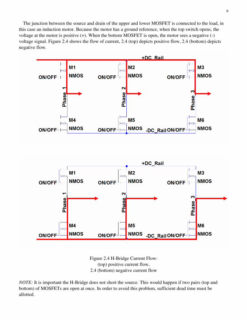
The junction between the source and drain of the upper and lower MOSFET is connected to the load, in
this case an induction motor. Because the motor has a ground reference, when the top switch opens, the
voltage at the motor is positive (+). When the bottom MOSFET is open, the motor sees a negative (-)
voltage signal. Figure 2.4 shows the flow of current, 2.4 (top) depicts positive flow, 2.4 (bottom) depicts
negative flow.
Figure 2.4 H-Bridge Current Flow:
(top) positive current flow,
2.4 (bottom) negative current flow
NOTE: It is important the H-Bridge does not short the source. This would happen if two pairs (top and
bottom) of MOSFETs are open at once. In order to avoid this problem, sufficient dead time must be
allotted.
10
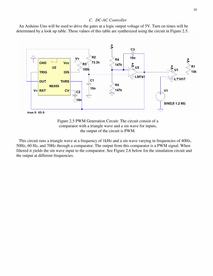
C. DC-AC Controller
An Arduino Uno will be used to drive the gates at a logic output voltage of 5V. Turn on times will be
determined by a look up table. These values of this table are synthesized using the circuit in Figure 2.5.
Figure 2.5 PWM Generation Circuit: The circuit consist of a
comparator with a triangle wave and a sin wave for inputs,
the output of the circuit is PWM.
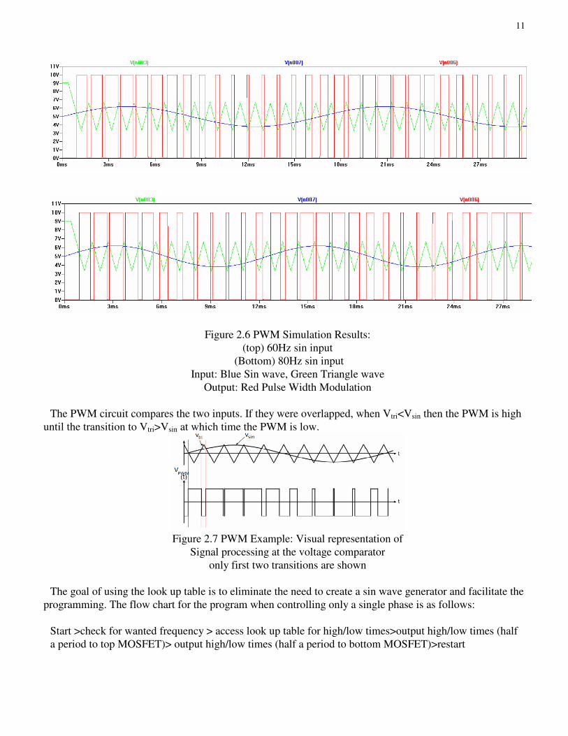
This circuit runs a triangle wave at a frequency of 1kHz and a sin wave varying in frequencies of 40Hz,
50Hz, 60 Hz, and 70Hz through a comparator. The output from this comparator is a PWM signal. When
filtered it yields the sin wave input to the comparator. See Figure 2.6 below for the simulation circuit and
the output at different frequencies.
11
Figure 2.6 PWM Simulation Results:
(top) 60Hz sin input
(Bottom) 80Hz sin input
Input: Blue Sin wave, Green Triangle wave
Output: Red Pulse Width Modulation
The PWM circuit compares the two inputs. If they were overlapped, when Vtri<Vsin then the PWM is high
until the transition to Vtri>Vsin at which time the PWM is low.
Figure 2.7 PWM Example: Visual representation of
Signal processing at the voltage comparator
only first two transitions are shown
The goal of using the look up table is to eliminate the need to create a sin wave generator and facilitate the
programming. The flow chart for the program when controlling only a single phase is as follows:
Start >check for wanted frequency > access look up table for high/low times>output high/low times (half
a period to top MOSFET)> output high/low times (half a period to bottom MOSFET)>restart

12
The reason for only choosing to run half of the period is that it will reduce the size of the look up table as
well as guarantee that there will be no time when both switches are on as the result of the program needing
to run through the complete string of numbers before it can restart and run them for the next MOSFET. In
other words, this guarantees dead time, as the program must restart the look up table process for every half
period.
D. Design Version 1 Evaluation
The Biggest error found with this design is the necessity for the micro-controller to operate with interrupts
at a speed of 10s of us. This is not possible as the ATMEGA chip has trouble operating at lower resolutions
than 10s of ms.
The next error is the MOSFET operation. It is difficult to turn on the MOSFET and keep it on even
though the selected MOSFETs (IRFP360) have a threshold voltage of 4V (the voltage that must be applied
at the Gate terminal for the switch to conduct). This turn on problem is due to the floating effect cause by
not referencing the H-Bridge to ground. Because of the configuration, the switches also tend to “stick” to a
position. When they are managed to be turned on, they cannot be turned off.
NOTE: Due to these errors being present at lower power scenarios, the configuration was not implemented
at high power levels.

13
III. HARDWARE DESIGN OVERVIEW (VERSION 2)
A. DC-AC Converter Update
The original converter was unable to function due to time limitations of the micro-controller as well as
problems with the “floating MOSFETs. The restructured program eliminates the look up table instead only
uses a single look up table for all frequencies instead of one table for each frequency. More look up tables
lead to an increased amount in storage space on the micro-controller IC. In this case the reduction frees up
space on the microcontroller.
The code used for the construction of the sin waves is a modified version of the code written by Martin
Nawrath under the name Arduino DDS Sin wave Generator. Originally, the code produces a sin wave PWM
signal based on the reference voltage seen at the wiper of a potentiometer (a voltage divider is created by
the potentiometer). This reference voltage then determines how fast the program reads through the look up
table to produce a series of highs and lows.
The modified version of the code takes out unnecessary bits of code, sets up additional timers, applies
delays, and outputs to multiple pins. In order to output a signal at different pins it is necessary to use
different times. These timers control the set up for the output. Two additional pins are needed for the
additional phases. The delay is not hard set; instead it runs off the initial look up table. Delay time is
changed depending on how fast the look up table is read through. This is achieved by starting the look up
sequence at a different value in the array for each phase. Three phases can be created using a single look up
table. Because there is 256 values in the look up table (0-255), a third (1/3) of that is 85 and two thirds (2/3)
is 170. Meaning that when the first phase is reading initial value (0), the second phase is reading 85th
value,
and the third is at the 170th
value.
The second Problem was keeping the transistors in the ON state. A solution to the problem is using a
MOSFET driver. IC GATE DRIVER HV 3PHASE 44-PLCC (part number IRS2336JTRPBF) from
International Rectifier was used. It uses a charge pump to drive the gate voltage higher than the rail voltage
or low by decreasing the voltage through an open collector circuit. This logic comes from manipulating the
new PWM output from the micro-controller discussed earlier in this section; which is fed into the driver.
The internal circuitry to the driver takes the logic level input and uses that to control the output which goes
to the MOSFTE gate.
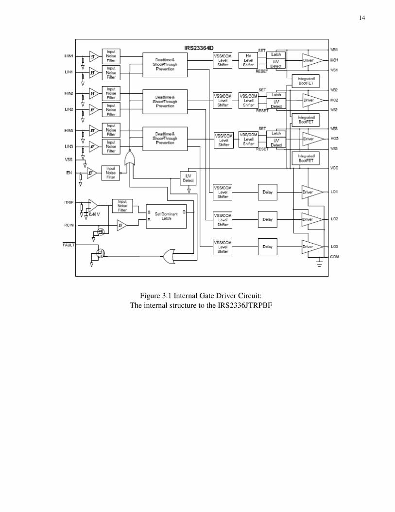
Figure 3.1 shows the internal structure to the Gate Driver. It first takes in a logic level signal which is fed
into a noise filtering circuit. Next it proceeds to a buffer where dead time (delay) is created; here the enable
signal for the IC is also taken into account. After that, it proceeds to level shifters that ensure the voltages
are within an operating window. Next, values are stored in a latch portion where its values are fed into the
driver or the open collector circuit. The driver turns on the MOSFET by applying power to the output pin of
the driver and powering the external circuitry (charge pump). The open collector acts as a drain which
dumps voltage at the gate to ground quickly, discharging both the charge pump and the parasitic
capacitance of the switch itself.
14
Figure 3.1 Internal Gate Driver Circuit:
The internal structure to the IRS2336JTRPBF
15
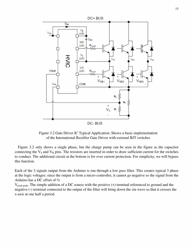
Figure 3.2 Gate Driver IC Typical Application: Shows a basic implementation
of the International Rectifier Gate Driver with external BJT switches
Figure 3.2 only shows a single phase, but the charge pump can be seen in the figure as the capacitor
connecting the VS and VB pins. The resistors are inserted in order to draw sufficient current for the switches
to conduct. The additional circuit at the bottom is for over current protection. For simplicity, we will bypass
this function.
Each of the 3 signals output from the Arduino is run through a low pass filter. This creates typical 3 phase
at the logic voltages; since the output is from a micro-controller, it cannot go negative so the signal from the
Arduino has a DC offset of ½
Vpeak-peak. The simple addition of a DC source with the positive (+) terminal referenced to ground and the
negative (-) terminal connected to the output of the filter will bring down the sin wave so that it crosses the
x-axis at one half a period.
16
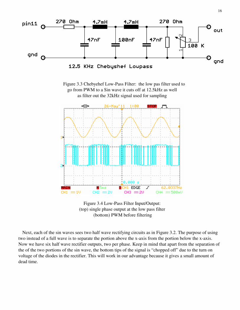
Figure 3.3 Chebyehef Low-Pass Filter: the low pas filter used to
go from PWM to a Sin wave it cuts off at 12.5kHz as well
as filter out the 32kHz signal used for sampling
Figure 3.4 Low-Pass Filter Input/Output:
(top) single phase output at the low pass filter
(bottom) PWM before filtering
Next, each of the sin waves sees two half wave rectifying circuits as in Figure 3.2. The purpose of using
two instead of a full wave is to separate the portion above the x-axis from the portion below the x-axis.
Now we have six half wave rectifier outputs, two per phase. Keep in mind that apart from the separation of
the of the two portions of the sin wave, the bottom tips of the signal is “chopped off” due to the turn on
voltage of the diodes in the rectifier. This will work in our advantage because it gives a small amount of
dead time.
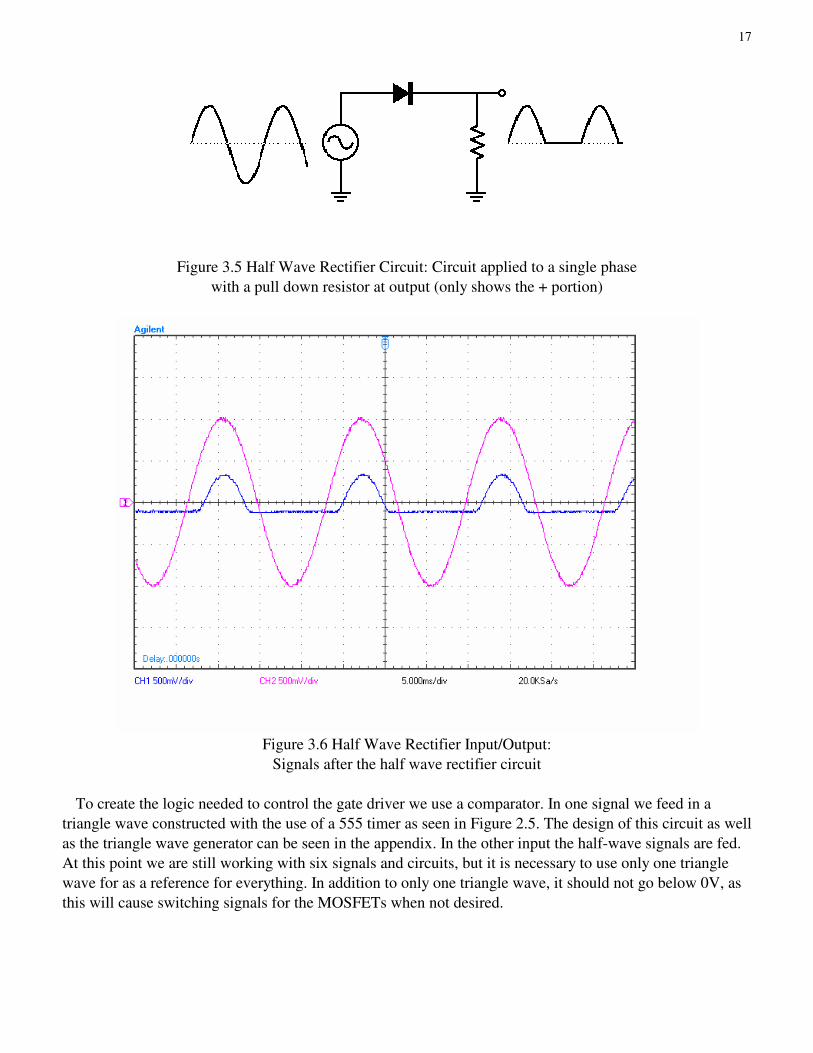
17
Figure 3.5 Half Wave Rectifier Circuit: Circuit applied to a single phase
with a pull down resistor at output (only shows the + portion)
Figure 3.6 Half Wave Rectifier Input/Output:
Signals after the half wave rectifier circuit
To create the logic needed to control the gate driver we use a comparator. In one signal we feed in a
triangle wave constructed with the use of a 555 timer as seen in Figure 2.5. The design of this circuit as well
as the triangle wave generator can be seen in the appendix. In the other input the half-wave signals are fed.
At this point we are still working with six signals and circuits, but it is necessary to use only one triangle
wave for as a reference for everything. In addition to only one triangle wave, it should not go below 0V, as
this will cause switching signals for the MOSFETs when not desired.

18
B. Design Version 2 Evaluation
The second design uses a half wave rectifier to split the control signal in to high and low so they can be
routed to its corresponding MOSFET. The main issue when using this approach is the voltage consumption
of the circuit. As seen in figure 3.5, the difference between the sin wave and the rectified wave is around
0.6V which is typical voltage consumption of the diode. The problem with this is that most of the signal is
consumed, and the dead time is close to 60% (30% coming from 2 half-wave circuits corresponding to 1
phase). The processing of the signal can also be reduced in the sense that there is no need for the triangle
wave when the PWM has already been generated. This will free up room on the circuit board, as well as
being more cost effective.

19
IV. HARDWARE DESIGN OVERVIEW (VERSION 3)
A. DC-AC Converter Update
The third version of motor drive again focuses on the revision of the DC-AC converter. It still uses the
Arduino with the same software. The difference is in the hardware that manipulates the signal. Directly
after the Arduino, we still have the low-pass filter, but the sin wave generated output from this filter is now
fed into two comparators (LM339 was used). The first comparator sees the sin wave at the positive (+)
input, while the second comparator sees it at the negative (-) input. The rails for the comparator are +5V for
the positive, and Ground for the negative with the reason being that the signal will only swing between
these values at the input to the comparators as well as on the output. The necessity for the two comparators
is to split the logic and create two enable signals: one for the high side and another for the low side.
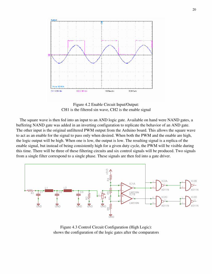
Figure 4.1 Low-Pass Filter with Comparators:
Connected to LM339 comparators
NOTE: a voltage divider sets the comparing voltage
The 3.3V is taken directly from the Arduino
Equation 4.1 nodal voltages
The additional terminal for the comparators will see a reference DC voltage. It will decide the dead time
in-between the transitions for the signal routing. As previously mentioned the dead time is needed to create
the time gape needed to ensure no cross over timer when both switches will be conducting at once.
The output for the comparators will be a square wave which changes in frequency with response to the
PWM output from the Arduino. They will match in frequency. The duty cycle is controlled by the dc
reference voltage at the additional input to the comparators. Two comparators are used to create two
separate signals with respect to both the positive and negative portions of the filtered sin wave (if the DC
offset is removed).
20
Figure 4.2 Enable Circuit Input/Output:
CH1 is the filtered sin wave, CH2 is the enable signal
The square wave is then fed into an input to an AND logic gate. Available on hand were NAND gates, a
buffering NAND gate was added in an inverting configuration to replicate the behavior of an AND gate.
The other input is the original unfiltered PWM output from the Arduino board. This allows the square wave
to act as an enable for the signal to pass only when desired. When both the PWM and the enable are high,
the logic output will be high. When one is low, the output is low. The resulting signal is a replica of the
enable signal, but instead of being consistently high for a given duty cycle, the PWM will be visible during
this time. There will be three of these filtering circuits and six control signals will be produced. Two signals
from a single filter correspond to a single phase. These signals are then fed into a gate driver.
Figure 4.3 Control Circuit Configuration (High Logic):
shows the configuration of the logic gates after the comparators

21
Figure 4.4 Important Control Circuit Waveforms:
The progression of the signals through the control circuit
CH1 is the filtered signal
CH2 is the enable signal after the comparators
CH3 is the logic fed into the gate driver after the NAND gates
The purpose of using a gate driver is the application of a charge pump circuit to the gate of the MOSFET.
By doing so, it allows the gate voltage to be lifted and maintain the ON position in the switch. It is an
application of the “bootstrap effect”. The circuit for the gate driver was designed according to the published
article: Design Tips: Using Monolithic High Voltage Gate Drivers, By: A. Merello, A. Rugginenti, and M.
Grasso.
B. Driver Component Sizing
Bootstrap Capacitor:
VCC – the IC voltage supply
VCEon – the emitter collector voltage (in this case Drain Source)
VF – bootstrap diode forward voltage
VGEmin – the min gate emitter voltage (Gate Drain)
Equation 4.2 finds the minimum voltage drop that guarantees the MOSFT is on

22
QG – Gate charge needed to turn ON
QLS – Charge required by the internal level shifters
ILK_GE – Gate Source leakage current
IQBS – Quiescent Current
ILK – Floating section leakage current
ILK_DIODE – Bootstrap diode leakage current
ILK_CAP – bootstrap capacitor leakage current
IDS – Desat diode bias (when ON)
THON – High side ON Time
Equation 4.3 uses equation 4.2 to calculate the needed capacitor voltage
NOTE: values take from data sheet; some may or may not apply depending on type of switch used
Bootstrap Diode:
The diode must have a BV > DC+ and a fast recovery time (<100ns) to minimize the amount of charge
fed back from the bootstrap capacitor to VCC supply.
For additional design strategies refer to article:
Design Tips: Using Monolithic High Voltage Gate Drivers By: A. Merello, A. Rugginenti, and M. Grasso.
Figure 4.5 Charge Pump Circuit:
The component connections made for a single phase on the driver

23
V. TESTING
A. Small Scale
The testing was broken down into two categories: small and large scale power circuits. The controlling
circuit was kept the same. The small scale testing was essential because the power handling capabilities of
the circuit at its initial prototype levels was not possible. Due to the large power demands, the large
IRFP360PBF MOSFETs from International Rectifier were traded in for smaller switches IRF510 from
International Rectifier as well. The DC rails were reduced to 10V and obtained from a DC power supply
instead of a rectified signal. Testing for the drive was done for a range of 40-80 Hz. Key nodes were probed
and their signals analyzed. The captures included in this report are the result of the small scale testing.
While a complete large scale test was not completed due to a lack of components (PCB), the small scale
test was a success. All the signals behaved as predicted. Additional testing is required, but must be done
using a combination of PCB to ensure proper connections as well as proper power capabilities.

24
VI. PCB DESIGN
The control circuit was separated from the power circuit as much as possible in an attempt to isolate any
induced voltages from the large currents seen in the power circuit. Included in the appendix are the gerber
files for both the control circuit and the power circuit. On the power circuit, the capacitors and the rectifier
will be mounted separately and jumpers used to link the parts. This was done to isolate any problems that
might be encounter as well as to save board space.

25
VII. CONTINUED WORK
This purpose of this area is to describe any additional steps that can be taken to improve the design if
more time was available.
A. Additional Features
Due to the applications for the motor drive, a GUI would be useful. In the original design, a user interface
was proposed; but due to the space restrictions on the Arduino in terms of timers and outputs, interfacing an
LCD screen and buttons was not possible.
Additional expansion of for this project would include the integration of pushbuttons that control a digital
potentiometer. Because the Arduino only depends on the reference voltage at the analog to digital converter
(ADC), the precise control of a digital potentiometer would be ideal. It would give more control over the
frequency selection, as well as keep the output stable (no wonder in the frequency output due to the
elimination of an analog wiper on the potentiometer.
The additional power supply rails for the logic level circuits are provided by a battery pack. Because the
unit is meant to stand alone, additional design work would be necessary to eliminate the need for a battery
pack. The only problem is the use of 3-phase as an input. Due to its high potential, large and costly
transformers would be required to step down the voltage to a safe level. A possible fix to the problem can
be the addition of a small solar array to keep a battery bank charged for use by the logic circuits.
Last suggestion would be the complete integration of all the separate parts into one PCB. I would suggest
that a Faraday Cage be added around the controlling circuit to shield it from any induced voltages from the
power circuit

26
VIII. CONCLUSION
The basic idea for this senior project was taken from the functional explanations of an H-Bridge as
described in Advanced Power Electronics: EE411 by Dr. Taufik and Dr. Dolan. The functionality and
principals of a PWM H-Bridge was used as a base for idea development. Unique circuitry was designed and
developed as needed for the motor drive. This report documents the development in chronological order as
problems with the original design were identified.
The main difference between the H-Bridges discussed in the text book and the one described in this paper
is the ability for selectable frequency outputs. A micro-controller provides the initial control signal and
analog circuitry processes the original signal into a usable control signal. The power circuit for the drive
consisted of a bridge rectifier, capacitor bank, and H-bridge. These are the most stable designs. The control
circuit can use the most improvement.

27
IX. REFERENCES
T a u f i k , a n d D o l a n , A d v a n c e d P o w e r E l e c t r o n i c s . 5 t h R e v i s i o n . S a n Lu i s O b i s p o :
C a l P o l y S t a t e U n i v e r s i t y , S a n Lu i s O b i s p o , 2 0 1 1 . P r i n t .
T a u f i k , a n d D o l a n , I n t r o d u c t i o n t o P o w e r E l e c t r o n i c s . 8 t h R e v i s i o n . S a n Lu i s
O b i s p o :
C a l P o l y S t a t e U n i v e r s i t y , S a n Lu i s O b i s p o , 2 0 1 0 . P r i n t .
F r a n c o , S . D e s i g n w i t h O p e r a t i o n a l A m p l i f i e r s a n d A n a l o g I n t e g r a t e d C i r c u i t s .
3 r d . M c G r a w - H i l l , 2 0 0 2 . 4 1 3 - 4 1 5 . P r i n t .
M e r e l l o , A . , A . R u gg i n e n t , a n d M . G r a s s o . "U s i n g M o n o l i t h i c H i gh V o l t a ge G a t e
D r i v e r s . " I n t e r n a t i o n a l R e c t i f i e r D a t a S h e e t . In t e r n a t i o n a l R e c t i f i e r , W e b .
< h t t p : / / w w w . i r f . c o m / t e c h n i c a l - i n f o / d e s i gn t p / d t 0 4 - 4 . p d f > .
P r o d a n o v , V l a d i m i r . "R e l a x a t i o n O s c i l l a t o r s w i t h 5 0 % D u t y C yc l e , T r i a n g l e
W a v e G e n e r a t o r s . " E E 4 0 9 Le c t u r e N o t e s . C a l P o l y S t a t e U n i v e r s i t y , S a n Lu i s
O b i s p o . S a n Lu i s O b i s p o . 1 1 / 2 / 2 0 1 0 . Le c t u r e .
P r o d a n o v , V l a d i m i r . "P u l s e - W i d t h M o d u l a t i o n . " E E 4 0 9 Le c t u r e N o t e s . C a l P o l y
S t a t e U n i v e r s i t y , S a n Lu i s O b i s p o . S a n Lu i s O b i s p o . 1 1 / 4 / 2 0 1 0 . Le c t u r e .
N a w r a t h , M a r t i n . "A r d u i n o D D S S i n e W a v e G e n e r a t o r . "L a b I I I : L a b o r a t o r y f o r
E x p e r i m e n t a l C o m p u t e r S c i e n c e a t t h e A c a d e m y o f M e d i a A r t s C o l o g n e . A c a d e m y
o f M e d i a A r t s C o l o gn e , n . d . W e b .
< h t t p : / / i n t e r f a c e . k h m . d e / i n d e x . p h p / l a b / e x p e r i m e n t s / a r d u i n o - d d s - s i n e w a v e -
ge n e r a t o r / > .
Data Sheets:
Three Phase Bridge (Power Modules), 25/35 A, Vishay, http://www.vishay.com/docs/93565/93565.pdf
Power MOSFET, Vishay Siliconix, http://www.vishay.com/docs/90292/sihfp360.pdf
Aluminum Capacitors, Power High Ripple Current, Screw Terminals, Vishay BC components,
http://www.vishay.com/docs/28371/101102ph.pdf
Quad Comparator, Fairchild Semiconductor, http://www.fairchildsemi.com/ds/LM/LM239A.pdf
High Voltage 3 Phase Gate Driver IC, International Rectifier, http://www.irf.com/product-
info/datasheets/data/irs2336.pdf
8-bit Microcontroller with 4/8/16/32K Bytes In-System Programmable Flash, Atmel,
http://www.atmel.com/dyn/resources/prod_documents/doc8161.pdf

28
X. APPENDIES
29
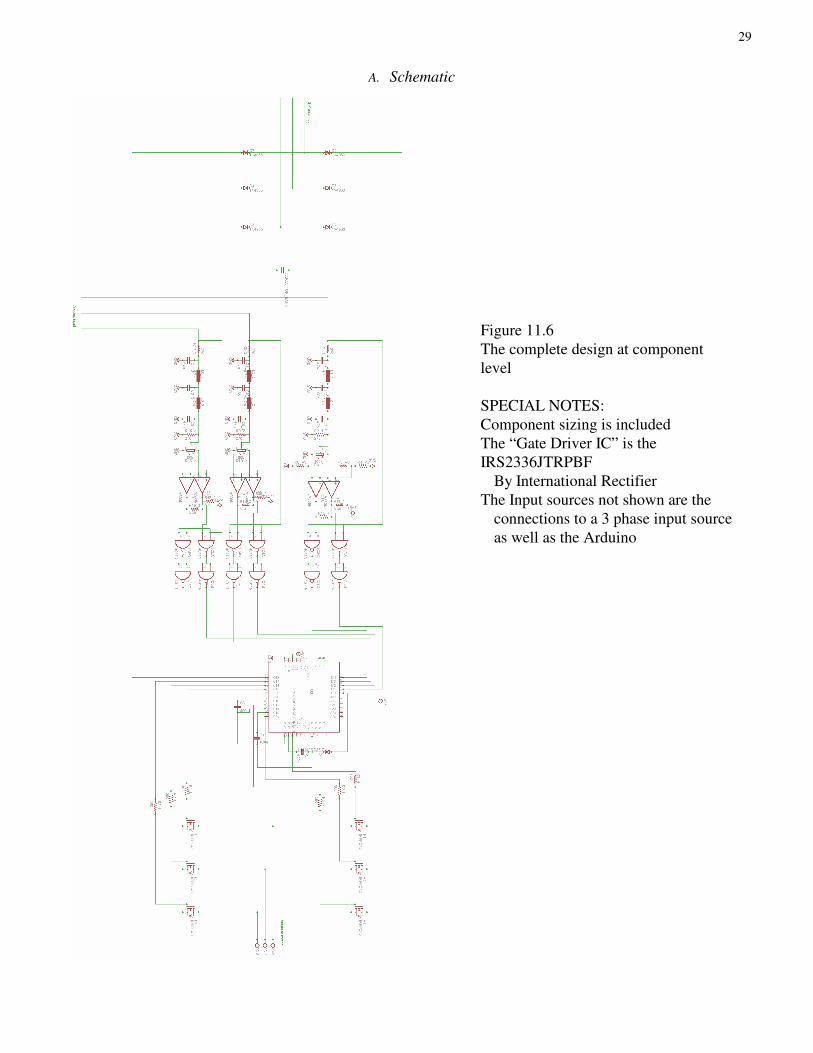
A. Schematic
Figure 11.6
The complete design at component
level
SPECIAL NOTES:
Component sizing is included
The “Gate Driver IC” is the
IRS2336JTRPBF
By International Rectifier
The Input sources not shown are the
connections to a 3 phase input source
as well as the Arduino

30
B. Parts List and Cost
Part Quantity Cost Per Unit
3-Phase Bridge Rectifier (p/n: 36MT80): 1 16.21
470uF Aluminum Capacitor 400V/3A (p/n: MAL210216471E3) 2 21.85
N-Channel Power MOSFET (p/n: IRFP360PBF) 6 6.80
3-Phase Gate Driver (p/n: IRS2336JTRPBF) 1 7.82
General Purpose Comparators (p/n:LM339) 2 0.75
100k Pot Multiple Turn 3 1.00
Single Turn 10k Pot 1 2.99
Arduino Uno (ATMEGA 328p) 1 29.95
4.7mH inductor (p/n: TSL0808RA-472JR13-PF) 6 1.28
IC Gate NAND (p/n: 74HC00N) 3 0.48
Assorted Resistors - -
Assorted Capacitors - -
Power Circuit PCB 1 79.90
Control Circuit PCB 1 79.90
Miscellaneous connectors - -
Total Cost
Per Unit
315.07
+miscellaneous parts and tax
31
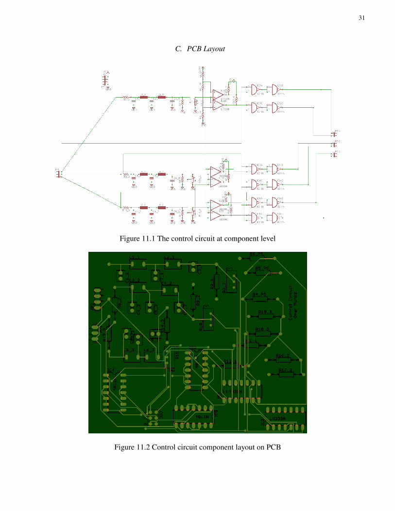
C. PCB Layout
Figure 11.1 The control circuit at component level
Figure 11.2 Control circuit component layout on PCB
32
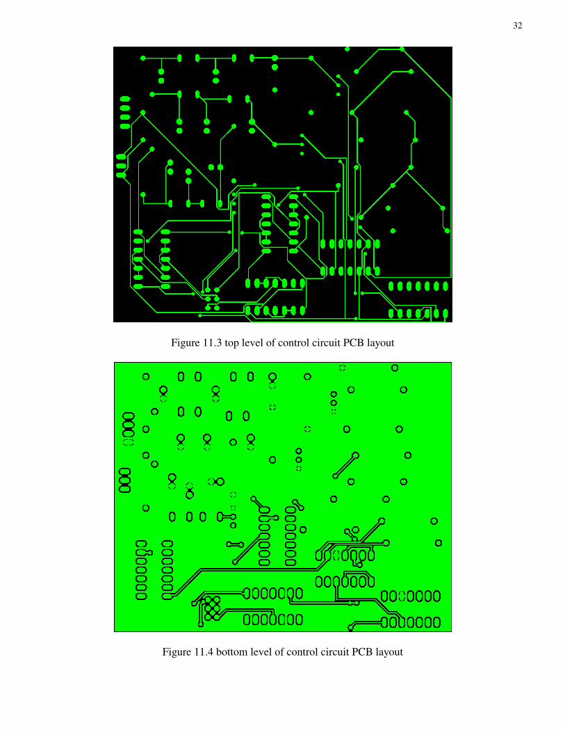
Figure 11.3 top level of control circuit PCB layout
Figure 11.4 bottom level of control circuit PCB layout
33
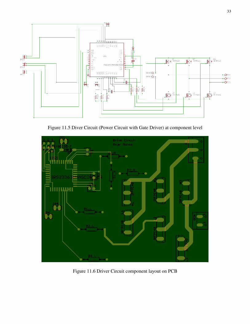
Figure 11.5 Diver Circuit (Power Circuit with Gate Driver) at component level
Figure 11.6 Driver Circuit component layout on PCB
34
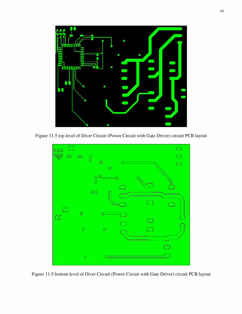
Figure 11.5 top level of Diver Circuit (Power Circuit with Gate Driver) circuit PCB layout
Figure 11.5 bottom level of Diver Circuit (Power Circuit with Gate Driver) circuit PCB layout

35
D. Arduino C Code
/******************************************************************
* DDS-sinewave - 3phase
*
******************************************************************/
#include "avr/pgmspace.h"
#include "avr/io.h"
// table of 256 sine values / one sine period / stored in flash memory
PROGMEM prog_uchar sine256[] =
{
127,130,133,136,139,143,146,149,152,155,158,161,164,167,170,173,176,178,181,184,187,190,192,195,198,200,203,205,208,2
10,212,215,217,219,221,223,225,227,229,231,233,234,236,238,239,240,242,243,244,245,247,248,249,249,250,251,252,252,25
3,253,253,254,254,254,254,254,254,254,253,253,253,252,252,251,250,249,249,248,247,245,244,243,242,240,239,238,236,234
,233,231,229,227,225,223,221,219,217,215,212,210,208,205,203,200,198,195,192,190,187,184,181,178,176,173,170,167,164,
161,158,155,152,149,146,143,139,136,133,130,127,124,121,118,115,111,108,105,102,99,96,93,90,87,84,81,78,76,73,70,67,64,
62,59,56,54,51,49,46,44,42,39,37,35,33,31,29,27,25,23,21,20,18,16,15,14,12,11,10,9,7,6,5,5,4,3,2,2,1,1,1,0,0,0,0,0,0,0,1,1,1,2,
2,3,4,5,5,6,7,9,10,11,12,14,15,16,18,20,21,23,25,27,29,31,33,35,37,39,42,44,46,49,51,54,56,59,62,64,67,70,73,76,78,81,84,87,
90,93,96,99,102,105,108,111,115,118,121,124
};
#define cbi(sfr, bit) (_SFR_BYTE(sfr) &= ~_BV(bit))
#define sbi(sfr, bit) (_SFR_BYTE(sfr) |= _BV(bit))
#define PWM_OUT_1 11 // PWM output on pin 11
#define PWM_OUT_2 10 // PWM output on pin 10
#define PWM_OUT_3 9 // PWM output on pin 9
#define LED_PIN 13 // LED status on pin 13
#define TEST_PIN 7 // Scope trigger on pin 7
#define POTEN_IN 0 // Potentiometer on pin 0
#define OFFSET_1 85 // Offset for second-phase
#define OFFSET_2 170 // Offset for third-phase
double dfreq;
const double refclk = 31376.6; // measured
const uint64_t twoTo32 = pow(2, 32); // compute value at startup and use as constant
// variables used inside interrupt service declared as voilatile
volatile uint8_t icnt; // var inside interrupt
volatile uint8_t icnt1; // var inside interrupt
volatile uint8_t c4ms; // counter incremented every 4ms
volatile uint32_t phase_accum; // pahse accumulator
volatile uint32_t tword_m; // dds tuning word m
//******************************************************************
void setup()
{
pinMode(LED_PIN, OUTPUT); // sets the digital pin as output
Serial.begin(115200); // connect to the serial port
Serial.println("DDS Test");

36
pinMode(TEST_PIN, OUTPUT); // sets the digital pin as output
pinMode(PWM_OUT_1, OUTPUT); // PWM output / frequency output
pinMode(PWM_OUT_2, OUTPUT); // PWM output / frequency output
pinMode(PWM_OUT_3, OUTPUT); // PWM output / frequency output
// Setup the timers
setup_timer1();
setup_timer2();
// disable interrupts to avoid timing distortion
cbi (TIMSK0, TOIE0); // disable Timer0 !!! delay() is now not available
sbi (TIMSK2, TOIE2); // enable Timer2 Interrupt
dfreq = 1000.0; // initial output frequency = 1000.0 Hz
tword_m = twoTo32 * dfreq / refclk; // calulate DDS new tuning word
}
//******************************************************************
void loop()
{
if (c4ms > 250) // timer / wait for a full second
{
c4ms = 0;
dfreq = analogRead(POTEN_IN); // read Poti on analog pin 0 to adjust output frequency from 0..1023 Hz
cbi (TIMSK2, TOIE2); // disble Timer2 Interrupt
tword_m = twoTo32 * dfreq / refclk; // calulate DDS new tuning word
sbi (TIMSK2, TOIE2); // enable Timer2 Interrupt
Serial.print(dfreq);
Serial.print(" ");
Serial.println(tword_m);
}
}
//******************************************************************
// timer1 setup
// set prscaler to 1, PWM mode to phase correct PWM, 16000000/512 = 31.25kHz clock
void setup_timer1(void)
{
// Timer1 Clock Prescaler to : 1
sbi (TCCR1B, CS10);
cbi (TCCR1B, CS11);
cbi (TCCR1B, CS12);
// Timer0 PWM Mode set to Phase Correct PWM
cbi (TCCR1A, COM1A0); // clear Compare Match
sbi (TCCR1A, COM1A1);
cbi (TCCR1A, COM1B0); // clear Compare Match
sbi (TCCR1A, COM1B1);
sbi (TCCR1A, WGM10); // Mode 1 / Phase Correct PWM
cbi (TCCR1A, WGM11);
cbi (TCCR1B, WGM12);
cbi (TCCR1B, WGM13);
}

37
//******************************************************************
// timer2 setup
// set prscaler to 1, PWM mode to phase correct PWM, 16000000/512 = 31.25kHz clock
void setup_timer2(void)
{
// Timer2 Clock Prescaler to : 1
sbi (TCCR2B, CS20);
cbi (TCCR2B, CS21);
cbi (TCCR2B, CS22);
// Timer2 PWM Mode set to Phase Correct PWM
cbi (TCCR2A, COM2A0); // clear Compare Match
sbi (TCCR2A, COM2A1);
sbi (TCCR2A, WGM20); // Mode 1 / Phase Correct PWM
cbi (TCCR2A, WGM21);
cbi (TCCR2B, WGM22);
}
//******************************************************************
// Timer2 Interrupt Service at 31.25kHz = 32us
// this is the timebase REFCLOCK for the DDS generator
// FOUT = (M (REFCLK)) / (2 exp 32)
// runtime : 8 microseconds ( inclusive push and pop)
ISR(TIMER2_OVF_vect)
{
sbi(PORTD, TEST_PIN); // Test / set PORTD,TEST_PIN high to observe timing with a oscope
phase_accum += tword_m; // soft DDS, phase accu with 32 bits
icnt = phase_accum >> 24; // use upper 8 bits for phase accu as frequency information
OCR2A = pgm_read_byte_near(sine256 + icnt); // read value fron ROM sine table and send to PWM DAC
OCR1A = pgm_read_byte_near(sine256 + (uint8_t)(icnt + OFFSET_1));
OCR1B = pgm_read_byte_near(sine256 + (uint8_t)(icnt + OFFSET_2));
if (icnt1++ == 125) // increment variable c4ms every 4 milliseconds
{
c4ms++;
icnt1 = 0;
}
cbi(PORTD, TEST_PIN); // reset PORTD,TEST_PIN
}


![Руководство по эксплуатации VFD-L062015].pdf · abelta pykoboactbo no vfd-l (220 b, 0.2-2.2 kbt) (115/230 b, 25 bt-ioo bt) vfd-l 0.75kw warning 5011609903-les4](https://img.pdfslide.tips/doc/110x75/600968378c1d1d2efe3b443e/f-f-vfd-l-062015pdf-abelta.jpg)